TWI835453B - Tapered upper electrode for uniformity control in plasma processing - Google Patents
Tapered upper electrode for uniformity control in plasma processingDownload PDFInfo
- Publication number
- TWI835453B TWI835453BTW111146973ATW111146973ATWI835453BTW I835453 BTWI835453 BTW I835453BTW 111146973 ATW111146973 ATW 111146973ATW 111146973 ATW111146973 ATW 111146973ATW I835453 BTWI835453 BTW I835453B
- Authority
- TW
- Taiwan
- Prior art keywords
- upper electrode
- substrate
- plasma
- region
- substrate processing
- Prior art date
Links
Images


Classifications
- H—ELECTRICITY
- H01—ELECTRIC ELEMENTS
- H01J—ELECTRIC DISCHARGE TUBES OR DISCHARGE LAMPS
- H01J37/00—Discharge tubes with provision for introducing objects or material to be exposed to the discharge, e.g. for the purpose of examination or processing thereof
- H01J37/32—Gas-filled discharge tubes
- H01J37/32431—Constructional details of the reactor
- H01J37/32532—Electrodes
- H01J37/32541—Shape
- H—ELECTRICITY
- H01—ELECTRIC ELEMENTS
- H01J—ELECTRIC DISCHARGE TUBES OR DISCHARGE LAMPS
- H01J37/00—Discharge tubes with provision for introducing objects or material to be exposed to the discharge, e.g. for the purpose of examination or processing thereof
- H01J37/02—Details
- H01J37/04—Arrangements of electrodes and associated parts for generating or controlling the discharge, e.g. electron-optical arrangement or ion-optical arrangement
- C—CHEMISTRY; METALLURGY
- C23—COATING METALLIC MATERIAL; COATING MATERIAL WITH METALLIC MATERIAL; CHEMICAL SURFACE TREATMENT; DIFFUSION TREATMENT OF METALLIC MATERIAL; COATING BY VACUUM EVAPORATION, BY SPUTTERING, BY ION IMPLANTATION OR BY CHEMICAL VAPOUR DEPOSITION, IN GENERAL; INHIBITING CORROSION OF METALLIC MATERIAL OR INCRUSTATION IN GENERAL
- C23C—COATING METALLIC MATERIAL; COATING MATERIAL WITH METALLIC MATERIAL; SURFACE TREATMENT OF METALLIC MATERIAL BY DIFFUSION INTO THE SURFACE, BY CHEMICAL CONVERSION OR SUBSTITUTION; COATING BY VACUUM EVAPORATION, BY SPUTTERING, BY ION IMPLANTATION OR BY CHEMICAL VAPOUR DEPOSITION, IN GENERAL
- C23C16/00—Chemical coating by decomposition of gaseous compounds, without leaving reaction products of surface material in the coating, i.e. chemical vapour deposition [CVD] processes
- C23C16/44—Chemical coating by decomposition of gaseous compounds, without leaving reaction products of surface material in the coating, i.e. chemical vapour deposition [CVD] processes characterised by the method of coating
- C23C16/455—Chemical coating by decomposition of gaseous compounds, without leaving reaction products of surface material in the coating, i.e. chemical vapour deposition [CVD] processes characterised by the method of coating characterised by the method used for introducing gases into reaction chamber or for modifying gas flows in reaction chamber
- C23C16/45561—Gas plumbing upstream of the reaction chamber
- C—CHEMISTRY; METALLURGY
- C23—COATING METALLIC MATERIAL; COATING MATERIAL WITH METALLIC MATERIAL; CHEMICAL SURFACE TREATMENT; DIFFUSION TREATMENT OF METALLIC MATERIAL; COATING BY VACUUM EVAPORATION, BY SPUTTERING, BY ION IMPLANTATION OR BY CHEMICAL VAPOUR DEPOSITION, IN GENERAL; INHIBITING CORROSION OF METALLIC MATERIAL OR INCRUSTATION IN GENERAL
- C23C—COATING METALLIC MATERIAL; COATING MATERIAL WITH METALLIC MATERIAL; SURFACE TREATMENT OF METALLIC MATERIAL BY DIFFUSION INTO THE SURFACE, BY CHEMICAL CONVERSION OR SUBSTITUTION; COATING BY VACUUM EVAPORATION, BY SPUTTERING, BY ION IMPLANTATION OR BY CHEMICAL VAPOUR DEPOSITION, IN GENERAL
- C23C16/00—Chemical coating by decomposition of gaseous compounds, without leaving reaction products of surface material in the coating, i.e. chemical vapour deposition [CVD] processes
- C23C16/44—Chemical coating by decomposition of gaseous compounds, without leaving reaction products of surface material in the coating, i.e. chemical vapour deposition [CVD] processes characterised by the method of coating
- C23C16/455—Chemical coating by decomposition of gaseous compounds, without leaving reaction products of surface material in the coating, i.e. chemical vapour deposition [CVD] processes characterised by the method of coating characterised by the method used for introducing gases into reaction chamber or for modifying gas flows in reaction chamber
- C23C16/45563—Gas nozzles
- C23C16/45565—Shower nozzles
- C—CHEMISTRY; METALLURGY
- C23—COATING METALLIC MATERIAL; COATING MATERIAL WITH METALLIC MATERIAL; CHEMICAL SURFACE TREATMENT; DIFFUSION TREATMENT OF METALLIC MATERIAL; COATING BY VACUUM EVAPORATION, BY SPUTTERING, BY ION IMPLANTATION OR BY CHEMICAL VAPOUR DEPOSITION, IN GENERAL; INHIBITING CORROSION OF METALLIC MATERIAL OR INCRUSTATION IN GENERAL
- C23C—COATING METALLIC MATERIAL; COATING MATERIAL WITH METALLIC MATERIAL; SURFACE TREATMENT OF METALLIC MATERIAL BY DIFFUSION INTO THE SURFACE, BY CHEMICAL CONVERSION OR SUBSTITUTION; COATING BY VACUUM EVAPORATION, BY SPUTTERING, BY ION IMPLANTATION OR BY CHEMICAL VAPOUR DEPOSITION, IN GENERAL
- C23C16/00—Chemical coating by decomposition of gaseous compounds, without leaving reaction products of surface material in the coating, i.e. chemical vapour deposition [CVD] processes
- C23C16/44—Chemical coating by decomposition of gaseous compounds, without leaving reaction products of surface material in the coating, i.e. chemical vapour deposition [CVD] processes characterised by the method of coating
- C23C16/50—Chemical coating by decomposition of gaseous compounds, without leaving reaction products of surface material in the coating, i.e. chemical vapour deposition [CVD] processes characterised by the method of coating using electric discharges
- C23C16/505—Chemical coating by decomposition of gaseous compounds, without leaving reaction products of surface material in the coating, i.e. chemical vapour deposition [CVD] processes characterised by the method of coating using electric discharges using radio frequency discharges
- C23C16/509—Chemical coating by decomposition of gaseous compounds, without leaving reaction products of surface material in the coating, i.e. chemical vapour deposition [CVD] processes characterised by the method of coating using electric discharges using radio frequency discharges using internal electrodes
- H—ELECTRICITY
- H01—ELECTRIC ELEMENTS
- H01J—ELECTRIC DISCHARGE TUBES OR DISCHARGE LAMPS
- H01J37/00—Discharge tubes with provision for introducing objects or material to be exposed to the discharge, e.g. for the purpose of examination or processing thereof
- H01J37/32—Gas-filled discharge tubes
- H01J37/32431—Constructional details of the reactor
- H01J37/3244—Gas supply means
- H—ELECTRICITY
- H01—ELECTRIC ELEMENTS
- H01J—ELECTRIC DISCHARGE TUBES OR DISCHARGE LAMPS
- H01J2237/00—Discharge tubes exposing object to beam, e.g. for analysis treatment, etching, imaging
- H01J2237/30—Electron or ion beam tubes for processing objects
- H01J2237/317—Processing objects on a microscale
- H01J2237/31701—Ion implantation
- H—ELECTRICITY
- H01—ELECTRIC ELEMENTS
- H01J—ELECTRIC DISCHARGE TUBES OR DISCHARGE LAMPS
- H01J2237/00—Discharge tubes exposing object to beam, e.g. for analysis treatment, etching, imaging
- H01J2237/32—Processing objects by plasma generation
- H01J2237/33—Processing objects by plasma generation characterised by the type of processing
- H01J2237/332—Coating
- H01J2237/3322—Problems associated with coating
- H01J2237/3323—Problems associated with coating uniformity
- H—ELECTRICITY
- H01—ELECTRIC ELEMENTS
- H01J—ELECTRIC DISCHARGE TUBES OR DISCHARGE LAMPS
- H01J2237/00—Discharge tubes exposing object to beam, e.g. for analysis treatment, etching, imaging
- H01J2237/32—Processing objects by plasma generation
- H01J2237/33—Processing objects by plasma generation characterised by the type of processing
- H01J2237/334—Etching
- H01J2237/3343—Problems associated with etching
- H01J2237/3344—Problems associated with etching isotropy
- H—ELECTRICITY
- H01—ELECTRIC ELEMENTS
- H01J—ELECTRIC DISCHARGE TUBES OR DISCHARGE LAMPS
- H01J37/00—Discharge tubes with provision for introducing objects or material to be exposed to the discharge, e.g. for the purpose of examination or processing thereof
- H01J37/32—Gas-filled discharge tubes
- H01J37/32009—Arrangements for generation of plasma specially adapted for examination or treatment of objects, e.g. plasma sources
- H01J37/32082—Radio frequency generated discharge
- H01J37/32091—Radio frequency generated discharge the radio frequency energy being capacitively coupled to the plasma
- H—ELECTRICITY
- H01—ELECTRIC ELEMENTS
- H01J—ELECTRIC DISCHARGE TUBES OR DISCHARGE LAMPS
- H01J37/00—Discharge tubes with provision for introducing objects or material to be exposed to the discharge, e.g. for the purpose of examination or processing thereof
- H01J37/32—Gas-filled discharge tubes
- H01J37/32431—Constructional details of the reactor
- H01J37/32715—Workpiece holder
- H01J37/32724—Temperature
- H—ELECTRICITY
- H01—ELECTRIC ELEMENTS
- H01L—SEMICONDUCTOR DEVICES NOT COVERED BY CLASS H10
- H01L21/00—Processes or apparatus adapted for the manufacture or treatment of semiconductor or solid state devices or of parts thereof
- H01L21/67—Apparatus specially adapted for handling semiconductor or electric solid state devices during manufacture or treatment thereof; Apparatus specially adapted for handling wafers during manufacture or treatment of semiconductor or electric solid state devices or components ; Apparatus not specifically provided for elsewhere
- H01L21/67005—Apparatus not specifically provided for elsewhere
- H01L21/67011—Apparatus for manufacture or treatment
- H01L21/67017—Apparatus for fluid treatment
- H01L21/67063—Apparatus for fluid treatment for etching
- H01L21/67069—Apparatus for fluid treatment for etching for drying etching
Landscapes
- Chemical & Material Sciences (AREA)
- Engineering & Computer Science (AREA)
- Plasma & Fusion (AREA)
- Physics & Mathematics (AREA)
- Analytical Chemistry (AREA)
- Chemical Kinetics & Catalysis (AREA)
- Materials Engineering (AREA)
- Mechanical Engineering (AREA)
- Metallurgy (AREA)
- Organic Chemistry (AREA)
- General Chemical & Material Sciences (AREA)
- Drying Of Semiconductors (AREA)
- Plasma Technology (AREA)
Abstract
Description
Translated fromChinese本揭露內容係關於用以控制基板處理系統中之處理均勻性的系統與方法。The present disclosure relates to systems and methods for controlling processing uniformity in substrate processing systems.
在此所提供之先前技術說明乃係為了大致呈現本揭露內容背景之目的。在該先前技術段落中所述之目前列名發明人之工作、以及不可以其他方式認定為申請時之先前技術的實施態樣敘述皆不被明示或暗示地承認為針對本揭露內容之先前技術。The prior art description provided herein is for the purpose of generally presenting the context of the present disclosure. The work of the currently listed inventors described in this prior art paragraph, and the description of embodiments of the prior art that may not otherwise be identified as prior art at the time of filing, are not expressly or implicitly admitted to be prior art with respect to the present disclosure. .
基板處理系統可用以處理例如半導體晶圓的基板。可在基板上執行的示範處理包含但不限於化學氣相沉積(CVD,chemical vapor deposition)、原子層沉積(ALD,atomic layer deposition)、導體蝕刻、介電質蝕刻、快速熱處理(RTP,rapid thermal processing)、離子植入、物理氣相沉積(PVD,physical vapor deposition)、及/或其他的蝕刻、沉積、或清潔處理。可將基板安置在位於基板處理系統之處理腔室內的基板支架(例如基座、靜電夾頭(ESC,electrostatic chuck)等等)上。在處理期間,可將氣體混合物導入到處理腔室內,並且可使用電漿來引發並維持化學反應。Substrate processing systems may be used to process substrates such as semiconductor wafers. Exemplary processes that can be performed on the substrate include, but are not limited to, chemical vapor deposition (CVD), atomic layer deposition (ALD), conductor etching, dielectric etching, rapid thermal processing (RTP) processing), ion implantation, physical vapor deposition (PVD, physical vapor deposition), and/or other etching, deposition, or cleaning processes. The substrate can be placed on a substrate holder (such as a base, an electrostatic chuck (ESC), etc.) located in a processing chamber of the substrate processing system. During processing, a gas mixture can be introduced into the processing chamber and a plasma can be used to initiate and sustain chemical reactions.
處理腔室包含各種構件,其包含但不限於基板支架、氣體分佈裝置(例如噴淋頭,其亦可相當於上電極)、電漿限制遮板等等。基板支架可包含陶瓷層,其被安置以支撐晶圓。例如,可在處理期間將晶圓夾持於陶瓷層。基板支架可包含邊緣環,其被安置在基板支架的外部分周圍,該外部分係例如位於基板支架的周邊之外及/或鄰近基板支架的周邊。邊緣環可被設置以將電漿限制於基板上方的容積、使基板邊緣處理性能最佳化、保護基板支架免於被電漿所侵蝕等等。電漿限制遮板可被安置在基板支架與噴淋頭之各者周圍,以進一步將電漿限制在基板上方的容積內。The processing chamber includes various components, including but not limited to substrate supports, gas distribution devices (such as shower heads, which can also be equivalent to upper electrodes), plasma limiting shields, and so on. The substrate support may include a ceramic layer positioned to support the wafer. For example, the wafer can be clamped to a ceramic layer during processing. The substrate support may include an edge ring disposed about an outer portion of the substrate support, eg, outside and/or adjacent the perimeter of the substrate support. Edge rings may be configured to confine plasma to the volume above the substrate, optimize substrate edge handling performance, protect the substrate holder from plasma erosion, etc. A plasma confinement shutter may be positioned around each of the substrate holder and showerhead to further confine the plasma within the volume above the substrate.
一種用於基板處理系統的上電極包含一下表面。該下表面包含一第一部分與一第二部分,並且面向電漿。該第一部分包含具有第一厚度的一第一表面區域。該第二部分包含具有變化厚度的一第二表面區域,以使該第二部分從第二厚度轉變至該第一厚度。An upper electrode for a substrate processing system includes a lower surface. The lower surface includes a first part and a second part and faces the plasma. The first portion includes a first surface area having a first thickness. The second portion includes a second surface area having a varying thickness such that the second portion transitions from the second thickness to the first thickness.
在其他特徵中,該第二厚度係相當於位在該上電極之中心處的該第二部分之高度。該第一部分具有第一半徑,該第二部分具有第二半徑,以及該第一半徑係大於該第二半徑。該第二半徑係對應於在該基板處理系統操作期間於該上電極下方所產生之電場的第三半徑。該第二半徑係大於或等於該第三半徑。In other features, the second thickness is equivalent to the height of the second portion located at the center of the upper electrode. The first portion has a first radius, the second portion has a second radius, and the first radius is greater than the second radius. The second radius corresponds to a third radius of an electric field generated under the upper electrode during operation of the substrate processing system. The second radius is greater than or equal to the third radius.
在其他特徵中,該第二表面區域為傾斜,以使該第二部分從該第二厚度漸縮至該第一厚度。該第二部分的坡度係對應於在該基板處理系統操作期間於該上電極下方所產生之電場。該第二表面區域為台階狀。該第二表面區域為彎曲狀。該第二表面區域為凸狀。該第二表面區域為片段直線狀。該上電極的頂點與隅角係按照0.5 mm-10 mm的半徑加以磨圓。該下表面更包含複數孔洞,該複數孔洞係設置成允許處理氣體從一氣體分佈裝置流動通過該上電極。In other features, the second surface area is sloped such that the second portion tapers from the second thickness to the first thickness. The slope of the second portion corresponds to the electric field generated beneath the upper electrode during operation of the substrate processing system. The second surface area is stepped. The second surface area is curved. The second surface area is convex. The second surface area is in the shape of linear segments. The apex and corners of the upper electrode are rounded with a radius of 0.5 mm-10 mm. The lower surface further includes a plurality of holes configured to allow processing gas to flow from a gas distribution device through the upper electrode.
在其他特徵中,一種氣體分佈裝置包含該上電極。該氣體分佈裝置係相當於一噴淋頭。一種基板處理系統包含該氣體分佈裝置。In other features, a gas distribution device includes the upper electrode. The gas distribution device is equivalent to a shower head. A substrate processing system includes the gas distribution device.
一種用於基板處理系統的氣體分佈裝置包含一桿部分與包含一上電極的一底部分。該上電極包含一下表面。該下表面包含一第一部分與一第二部分,並且面向電漿。該第一部分具有第一厚度並且包含平坦的一第一表面區域。該第二部分包含具有變化厚度的一第二表面區域,以使該第二部分從第二厚度轉變至該第一厚度。A gas distribution device for a substrate processing system includes a rod portion and a base portion including an upper electrode. The upper electrode contains the lower surface. The lower surface includes a first part and a second part and faces the plasma. The first portion has a first thickness and includes a flat first surface area. The second portion includes a second surface area having a varying thickness such that the second portion transitions from the second thickness to the first thickness.
在其他特徵中,該第二表面區域為傾斜,以使該第二部分從該第二厚度漸縮至該第一厚度。該第二表面區域為台階狀。該第二表面區域為彎曲狀。該第二表面區域為凸狀。該第二表面區域為片段直線狀。該上電極的頂點與隅角係按照0.5 mm-10.0 mm的半徑加以磨圓。In other features, the second surface area is sloped such that the second portion tapers from the second thickness to the first thickness. The second surface area is stepped. The second surface area is curved. The second surface area is convex. The second surface area is in the shape of linear segments. The apex and corners of the upper electrode are rounded with a radius of 0.5 mm-10.0 mm.
一種用於基板處理系統的上電極包含一第一部分與一第二部分,該第一部分具有一第一表面區域,以及該第二部分延伸超出該第一表面區域並且相對於該上電極之中心而對稱地設置。該第二部分具有一頂點與一外周邊,並且從該頂點往該外周邊漸縮。An upper electrode for a substrate processing system includes a first portion and a second portion, the first portion having a first surface area, and the second portion extending beyond the first surface area and relative to the center of the upper electrode. Set symmetrically. The second part has an apex and an outer periphery, and is tapered from the apex toward the outer periphery.
在其他特徵中,該第一表面區域為平坦及/或凹狀。該頂點係與該上電極的該中心對正。該第一部分具有第一半徑,該第二部分具有第二半徑,以及該第一半徑係大於該第二半徑。該第二半徑係對應於在該基板處理系統操作期間於該上電極下方所產生之電場的第三半徑。該第二半徑係大於或等於該第三半徑。In other features, the first surface area is flat and/or concave. The vertex is aligned with the center of the upper electrode. The first portion has a first radius, the second portion has a second radius, and the first radius is greater than the second radius. The second radius corresponds to a third radius of an electric field generated under the upper electrode during operation of the substrate processing system. The second radius is greater than or equal to the third radius.
在其他特徵中,該第二部分的坡度係對應於在該基板處理系統操作期間於該上電極下方所產生之電場。該第二部分為下列至少一者:台階狀、彎曲狀、凸狀、以及片段直線狀。該第一與第二部分係面向基板。該第一與第二部分之至少一者更包含複數孔洞,該複數孔洞係設置成允許處理氣體從一氣體分佈裝置流動通過該上電極。In other features, the slope of the second portion corresponds to an electric field generated beneath the upper electrode during operation of the substrate processing system. The second part is at least one of the following: stepped, curved, convex, and segmented linear. The first and second portions face the substrate. At least one of the first and second portions further includes a plurality of holes configured to allow processing gas to flow from a gas distribution device through the upper electrode.
由詳細說明、申請專利範圍、及圖式,本揭露內容之其他領域的可應用性將變得顯而易見。詳細說明與具體範例僅係為了例示之目的而提出,並非意指限制本揭露內容的範圍。The applicability of the present disclosure to other fields will become apparent from the detailed description, patent claims, and drawings. The detailed description and specific examples are provided for purposes of illustration only and are not intended to limit the scope of the present disclosure.
蝕刻處理的若干實施樣態可依照基板處理系統、基板、氣體混合物、溫度、射頻(RF,radio frequency)與RF功率等等的特性而變化。例如,流動型態、以及因此之蝕刻速率與蝕刻均勻性,可依照基板處理系統之處理腔室內的構件之尺寸而變化。在若干示範處理中,整體蝕刻速率係隨著基板之上表面與氣體分佈裝置之底表面之間的距離增加而變化。又,蝕刻速率可從基板之中心到基板之外周邊而變化。例如,在基板之外周邊,鞘彎曲以及離子入射角偏斜可能會引起高縱橫比接觸窗(HARC,high aspect ratio contact)輪廓偏斜,電漿密度降低可能會引起蝕刻速率與蝕刻深度下降(roll off),以及與反應性物種(例如蝕刻劑及/或沉積前驅物)相關聯的化學負荷(chemical loading)可能會引起特徵關鍵尺寸(CD,critical dimension)不均勻性。又,例如蝕刻副產物的物質可被再沉積於基板上。蝕刻速率可依照其他處理參數而變化,該等處理參數包含但不限於RF與RF功率、溫度、以及橫越基板之上表面的氣體流動速度。Several implementations of the etching process may vary depending on the characteristics of the substrate processing system, substrate, gas mixture, temperature, radio frequency (RF), RF power, etc. For example, the flow pattern, and thus the etch rate and etch uniformity, may vary depending on the dimensions of the components within the processing chamber of the substrate processing system. In several exemplary processes, the overall etch rate varied as the distance between the upper surface of the substrate and the bottom surface of the gas distribution device increased. Also, the etching rate may vary from the center of the substrate to the outer periphery of the substrate. For example, outside the substrate periphery, sheath bending and ion incident angle deflection may cause high aspect ratio contact (HARC) profile deflection, and reduced plasma density may cause etching rate and etching depth to decrease ( feature critical dimension (CD) non-uniformity. Alternatively, substances such as etching by-products may be redeposited onto the substrate. The etch rate may vary according to other processing parameters including, but not limited to, RF and RF power, temperature, and gas flow velocity across the surface above the substrate.
可能影響基板之處理的構件包含但不限於氣體分佈裝置(例如噴淋頭,其亦可相當於上電極)、電漿限制遮板、及/或包含底板、一或多個邊緣環、耦接環等等的基板支架。例如,介電質電漿蝕刻處理可使用具有面向電漿之平坦底表面的上電極。在若干應用中,高射頻(RF)電源(例如設置在60 MHz、40 MHz等等的RF電源)可能會在基板上方的處理容積中引起中心尖峰(center-peaked)電漿分佈。又,高偏壓功率(例如設置在400 kHz、2 MHz等等的偏壓功率)可能會在基板的邊緣區域中引起電漿密度尖峰(例如距離中心介於80-150 mm處的邊緣尖峰)。包含中心尖峰與邊緣尖峰的電漿分佈可被稱為『W』形徑向電漿不均勻性。Components that may affect the processing of the substrate include, but are not limited to, gas distribution devices (such as showerheads, which may also be equivalent to the upper electrode), plasma confinement shields, and/or include the base plate, one or more edge rings, couplings Rings and other substrate supports. For example, a dielectric plasma etch process may use an upper electrode with a flat bottom surface facing the plasma. In some applications, high radio frequency (RF) power supplies (eg, those set at 60 MHz, 40 MHz, etc.) may cause center-peaked plasma distribution in the processing volume above the substrate. Also, high bias powers (e.g., those set at 400 kHz, 2 MHz, etc.) may cause plasma density spikes in the edge regions of the substrate (e.g., edge spikes between 80-150 mm from the center). . The plasma distribution containing a central peak and an edge peak can be called a "W"-shaped radial plasma inhomogeneity.
因此,不均勻的電漿分佈可能會引起不均勻的處理結果(例如蝕刻)。在若干應用(例如高縱橫比蝕刻應用)中,除了橫越基板的蝕刻不均勻性以外,徑向電漿不均勻性可能會造成輪廓偏斜。當縱橫比增加(例如大於50的縱橫比)時,輪廓偏斜的公差減小並且會期望極小的偏斜(例如小於0.1° )。Therefore, non-uniform plasma distribution may cause non-uniform processing results (eg, etching). In several applications, such as high aspect ratio etch applications, radial plasma non-uniformity may cause profile deflection in addition to etch non-uniformity across the substrate. As the aspect ratio increases (eg, aspect ratios greater than 50), the tolerance for profile deflection decreases and very small deflections (eg, less than 0.1°) may be expected.
依照本揭露內容之原理的系統與方法係修改上電極的尺寸與幾何形狀(例如輪廓),以控制徑向電漿分佈與均勻性。例如,使用具有漸縮(即,斜向、傾斜、偏斜、彎曲、成型等等)、面向電漿之下表面的上電極。在一範例中,上電極係在徑向上從中心朝向上電極之外周邊漸縮。在若干範例中,該漸縮可不延伸到上電極的外周邊,而係可停止在外周邊之徑向內側的一距離處。在其他範例中,該漸縮可延伸到上電極的外周邊。因此,上電極的厚度係基於從上電極之中心起算的徑向距離而變化。Systems and methods consistent with principles of the present disclosure modify the size and geometry (eg, profile) of the upper electrode to control radial plasma distribution and uniformity. For example, use an upper electrode with a tapered (ie, beveled, sloped, deflected, curved, shaped, etc.), plasma-facing lower surface. In one example, the upper electrode tapers radially from the center toward the outer periphery of the upper electrode. In some examples, the taper may not extend to the outer perimeter of the upper electrode, but may stop a distance radially inward of the outer perimeter. In other examples, the taper may extend to the outer perimeter of the upper electrode. Therefore, the thickness of the upper electrode varies based on the radial distance from the center of the upper electrode.
可依照期望的徑向電漿分佈來選擇漸縮的尺寸(例如在上電極之徑向距離處的相應厚度、漸縮的半徑或長度等等)。例如,可依照在上電極之中心的尖峰電漿密度來決定漸縮的厚度。相反地,可依照徑向電漿密度梯度的長度尺度來決定漸縮的半徑或長度。選擇在上電極之中心之漸縮的厚度,以降低並消除在處理容積之中心的尖峰電漿密度,並且選擇漸縮的半徑或長度,以降低(即,消除)並且最小化在徑向上的電漿不均勻性。因此,可使高縱橫比蝕刻中之電漿不均勻性所引起的輪廓偏斜與蝕刻不均勻性最小化。The size of the taper can be selected according to the desired radial plasma distribution (eg, corresponding thickness at radial distance from the upper electrode, radius or length of the taper, etc.). For example, the thickness of the taper may be determined by the peak plasma density at the center of the upper electrode. Instead, the radius or length of the taper can be determined by the length scale of the radial plasma density gradient. The tapered thickness at the center of the upper electrode is selected to reduce and eliminate peak plasma density at the center of the treatment volume, and the tapered radius or length is selected to reduce (i.e., eliminate) and minimize the peak plasma density in the radial direction. Plasma inhomogeneity. Therefore, profile deflection and etch non-uniformity caused by plasma non-uniformity in high aspect ratio etching can be minimized.
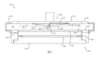
現在參考圖1,顯示一示範基板處理系統100。僅作為示範,基板處理系統100可用於執行使用RF電漿的蝕刻、沉積、及/或其他合適的基板處理。基板處理系統100包含處理腔室102,該處理腔室圍住基板處理系統100的其他構件並且容納RF電漿。基板處理腔室102包含上電極104以及例如靜電夾頭(ESC)的基板支架106。在操作期間,基板108被安置在基板支架106上。雖然特定的基板處理系統100與腔室102被顯示作為一範例,但本揭露內容的原理可被應用於其他類型的基板處理系統與腔室。Referring now to FIG. 1, an exemplary
僅作為示範,上電極104可包含氣體分佈裝置,例如導入並且分佈處理氣體的噴淋頭109。噴淋頭109可包含桿部分,該桿部分包含連接至處理腔室之頂表面的一端。底部分通常為圓柱形,並且於徑向上從位在與處理腔室之頂表面隔開的位置處之桿部分的相反端朝外延伸。噴淋頭之底部分的面向基板表面或面板(faceplate)包含複數孔洞,處理氣體或吹掃氣體(purge gas)流過該複數孔洞。或者,上電極104可包含引導板,以及處理氣體可以另一方式被導入。依照本揭露內容之原理的上電極104可具有如在下文中所詳述之漸縮、面向電漿的下表面。By way of example only,
基板支架106包含作為下電極的導電性底板110。底板110支撐陶瓷層112。在若干範例中,陶瓷層112可包含加熱層,例如陶瓷多區加熱板。耐熱層114(例如接合層)可被安置在陶瓷層112與底板110之間。底板110可包含一或多個冷媒通道116,該冷媒通道用以使冷媒流過底板110。基板支架106可包含邊緣環118,該邊緣環被安置以圍繞基板108的外周邊。The
RF產生系統120產生RF功率並且將其輸出至上電極104與下電極(例如基板支架106的底板110)之其中一者。上電極104與底板110之其中另一者可被DC接地、RF接地或浮動。僅作為示範,RF產生系統120可包含產生RF功率的RF功率產生器122,該RF功率係藉由匹配與分佈網路124而被饋送至上電極104或底板110。在其他範例中,可感應地或遠程地產生電漿。雖然,如為了示範目的所示,RF產生系統120係相當於電容耦合電漿(CCP,capacitively coupled plasma)系統,但本揭露內容的原理亦可實現在其他適當的系統中,例如,僅作為示範,變壓器耦合電漿(TCP,transformer coupled plasma)系統、CCP陰極系統、遠程微波電漿產生與輸送系統等等。The
氣體輸送系統130包含一或多個氣體源132-1、132-2、…以及132-N(統稱為氣體源132),於此處,N為大於零的整數。氣體源供應一或多個氣體混合物。氣體源亦可供應吹掃氣體。汽化前驅物亦可被使用。氣體源132係藉由閥134-1、134-2、…以及134-N(統稱為閥134)與質量流量控制器136-1、136-2、…以及136-N(統稱為質量流量控制器136)而連接至歧管140。歧管140的輸出被饋送至處理腔室102。僅作為示範,歧管140的輸出被饋送至噴淋頭109。The
溫度控制器142可連接至複數加熱元件,例如安置在陶瓷層112中的熱控制元件(TCE,thermal control elements)144。例如,加熱元件144可包含但不限於對應於多區加熱板中之個別區域的大型加熱元件及/或配置橫越多區加熱板之多個區域的微型加熱元件之陣列。溫度控制器142可用以控制複數加熱元件144,以控制基板支架106與基板108的溫度分佈。The
溫度控制器142可與冷媒組件146通訊,以控制通過通道116的冷媒流動。例如,冷媒組件146可包含冷媒幫浦與貯槽。溫度控制器142操作冷媒組件146,以選擇性地使冷媒流過通道116而冷卻基板支架106。
閥150與幫浦152可用以將蝕刻副產物從處理腔室102抽空。系統控制器160可用以控制基板處理系統100的構件。一或多個機器人170可用以將基板輸送到基板支架106上並且將基板從該基板支架移除。例如,機器人170可在EFEM 171與承載室172之間、在該承載室與VTM 173之間、在VTM 173與基板支架106之間等等傳送基板。雖然係顯示成分開的控制器,但溫度控制器142可實現於系統控制器160內。在若干範例中,保護密封件176可設置在位於陶瓷層112與底板110之間的接合層114的周邊周圍。
在若干範例中,處理腔室102可包含電漿限制遮板180,例如C形遮板。C形遮板180被安置在上電極104與基板支架106周圍,以將電漿限制在電漿區域182內。在若干範例中,C形遮板180包含半導體材料,例如矽(Si)或多晶矽。C形遮板180可包含一或多個槽孔184,該槽孔被安置以允許氣體流出電漿區域182,該電漿區域係待經由閥150與幫浦152而從處理腔室102排氣。In several examples, processing
現在參考圖2,顯示包含基板支架204以及氣體分佈裝置208(例如噴淋頭)的一示範基板處理腔室200。基板支架204包含可作為下電極的底板212。相反地,氣體分佈裝置208可包含上電極216。在若干範例中,上電極216可包含內電極220與外電極224。例如,內電極220與外電極224可分別相當於盤及環狀環(即,外電極224圍繞內電極220的外緣)。為了簡單起見,如在此所使用,本揭露內容會將內電極220與外電極224統稱為上電極216。Referring now to FIG. 2, an exemplary
底板212支撐陶瓷層228。陶瓷層228支撐基板232。在若干範例中,接合層236係安置在陶瓷層228與底板212之間,以及保護密封件240係設置在位於陶瓷層228與底板212之間的接合層236的周邊周圍。基板支架204可包含邊緣環242,該邊緣環被安置以圍繞基板232的外周邊。在若干範例中,處理腔室200可包含安置在上電極216周圍的電漿限制遮板244。上電極216、基板支架204(例如陶瓷層228)、邊緣環242、以及電漿限制遮板244界定出位在基板232上方的一處理容積(例如電漿區域)248。
如圖2所示,上電極216的下表面252為實質上平坦並且面向電漿。例如,下表面252為平坦,具有相對於處理腔室200的水平定向,並且平行於基板232與陶瓷層228。如在256處所顯示,具有平坦下表面252的上電極216造成中心尖峰電漿密度分佈(『電漿分佈』)。因此,電漿分佈為不均勻且包含中心尖峰260(即,相對於處理容積248與上電極216而位於中心之在垂直z方向上的密度尖峰),並可在r方向(即,徑向)上減少。電漿分佈可更包含外尖峰264。圖2所示之電漿分佈可造成處理不均勻性,例如基板232(如在基板232之中間半徑區域中)的輪廓偏斜與蝕刻不均勻性。As shown in Figure 2, the
例如,電漿分佈係由對應的RF電場(E場)分佈以及其到電漿中之功率蓄積(power deposition)所引起。E場分佈係取決於與施加之RF對應之所產生的電漿中的有效RF波長,因此E場分佈通常係與電漿分佈有關聯。例如,在圖2中,E場分佈可類似於在256處所顯示的電漿分佈。因此,E場分佈在與電漿分佈之中心尖峰260對應的區域中可為較大,並且在r方向上減少(即,隨著半徑增加而減少)。換言之,E場分佈在某距離上係表現出徑向衰減。For example, the plasma distribution is caused by the corresponding RF electric field (E-field) distribution and its power deposition into the plasma. The E-field distribution depends on the effective RF wavelength in the resulting plasma corresponding to the applied RF, so the E-field distribution is generally related to the plasma distribution. For example, in Figure 2, the E-field distribution may be similar to the plasma distribution shown at 256. Therefore, the E-field distribution may be larger in the region corresponding to the
在CCP系統中,用以產生電漿的RF功率產生垂直方向上之E場分佈的電容分量Ez,此引起電容電漿加熱。因此,當有效RF波長接近或小於基板半徑時,在電漿分佈之中心尖峰260的區域中,電容電漿加熱係被增加。相反地,在中心尖峰260的區域中,徑向上之E場分佈的電感分量Er實質上為零。換言之,與圖2所示之電漿分佈對應的E場分佈可相當於E = Ez,於此處,在中心尖峰260的區域中,Er = 0。In a CCP system, the RF power used to generate the plasma produces a capacitive component Ez of the E-field distribution in the vertical direction, which causes capacitive plasma heating. Therefore, capacitive plasma heating is increased in the region of the
現在參考圖3,顯示包含基板支架304與氣體分佈裝置308(例如噴淋頭)的另一示範基板處理腔室300。基板支架304包含可作為下電極的底板312。相反地,氣體分佈裝置308可包含上電極316。在若干範例中,上電極316可包含內電極320與外電極324。例如,內電極320與外電極324可分別相當於同心的盤及環(即,外電極324圍繞內電極320的外緣)。為了簡單起見,如在此所使用,本揭露內容會將內電極320與外電極324統稱為上電極316。Referring now to FIG. 3 , another exemplary
底板312支撐陶瓷層328。陶瓷層328支撐基板332。在若干範例中,接合層336係安置在陶瓷層328與底板312之間,以及保護密封件340係設置在位於陶瓷層328與底板312之間的接合層336的周邊周圍。基板支架304可包含邊緣環342,該邊緣環被安置以圍繞基板332的外周邊。在若干範例中,處理腔室300可包含安置在上電極316周圍的電漿限制遮板344。上電極316、基板支架304(例如陶瓷層328)、邊緣環342、以及電漿限制遮板344界定出位在基板332上方的一處理容積(例如電漿區域)348。
如圖3所示,上電極316的下表面352為漸縮並且面向電漿。例如,下表面352包含具有第一厚度且通常為平坦的第一部分356、以及漸縮(即傾斜)的第二部分360。第二部分360隨著半徑R(即,從中心364起算的距離)增加而從位在下表面352之中心364處的高度H開始減少。因此,第二部分360的厚度隨著半徑增加而變化(例如減少)。如在368處所顯示,具有漸縮下表面352的上電極316抑制電漿分佈的中心尖峰。換言之,如圖3所示的電漿分佈並不包含如圖2所示的中心尖峰260。又,漸縮的第二部分360促進從小間隙區域(即,在中心區域372中)到大間隙區域(即,在外區域376中)的電漿擴散,並因此降低在中心區域372中的電漿密度。As shown in Figure 3, the
與圖2的範例相比,漸縮下表面352在中心區域372中造成垂直方向上的降低電容E場分量Ez並且產生徑向上的非零電感E場分量Er。電感分量Er提供感應電漿加熱,此有效產生電漿。又,電感分量Er係隨著半徑R增加而增加。因此,由於電感分量Er係隨著半徑而增加且電容分量Ez係隨著半徑而減少,所以電感分量Er補償因電容分量Ez減少所引起之電漿分佈與加熱的變動。換言之,對應於圖3所示之電漿分佈的E場E可相當於E = Ez + Er,此係結合電容分量Ez與電感分量Er兩者並因此導致具有受抑制之中心尖峰的更均勻電漿分佈。Compared to the example of FIG. 2, tapered
現在參考圖4,顯示包含基板支架404與氣體分佈裝置408(例如噴淋頭)的另一示範基板處理腔室400。基板支架404包含可作為下電極的底板412。相反地,氣體分佈裝置408可包含上電極416。在若干範例中,上電極416可包含內電極420與外電極424。例如,內電極420與外電極424可分別相當於同心的盤及環(即,外電極424圍繞內電極420的外緣)。為了簡單起見,如在此所使用,本揭露內容會將內電極420與外電極424統稱為上電極416。Referring now to FIG. 4 , another exemplary
底板412支撐陶瓷層428。陶瓷層428支撐基板432。在若干範例中,接合層436係安置在陶瓷層428與底板412之間,以及保護密封件440係設置在位於陶瓷層428與底板412之間的接合層436的周邊周圍。基板支架404可包含邊緣環442,該邊緣環被安置以圍繞基板432的外周邊。在若干範例中,處理腔室400可包含安置在上電極416周圍的電漿限制遮板444。上電極416、基板支架404(例如陶瓷層428)、邊緣環442、以及電漿限制遮板444界定出位在基板432上方的一處理容積(例如電漿區域)448。
如圖4所示,上電極416的下表面452為漸縮並且面向電漿。例如,下表面452包含具有第一厚度且通常為平坦的第一部分456、以及漸縮(即傾斜)的第二部分460。第二部分460隨著半徑R(即,從中心464起算的距離)增加而從位在下表面452之中心464處的高度H開始減少。因此,第二部分460的厚度隨著半徑增加而變化(例如減少)。如在468處所顯示,具有漸縮下表面452的上電極416抑制電漿分佈的中心尖峰。換言之,如圖4所示的電漿分佈並不包含如圖2所示的中心尖峰260。又,漸縮的第二部分460促進從小間隙區域(即,在中心區域472中)到大間隙區域(即,在外區域476中)的電漿擴散,並因此降低在中心區域472中的電漿密度。As shown in Figure 4, the
類似於圖3之範例,在中心區域472中,漸縮下表面452造成垂直方向上的降低電容E場分量Ez並且產生徑向上的非零電感E場分量Er。因此,由於電感分量Er係隨著半徑而增加且電容分量Ez係隨著半徑而減少,所以電感分量Er補償因電容分量Ez減少所引起之電漿分佈與加熱的變動。與圖3的範例相比,相較於第二部分360的漸縮部,第二部分460的漸縮部具有較小的坡度並且較為平緩(即,隨著半徑增加,第二部分460的厚度係以較低的速率或角度減少)。因此,橫越基板432的電漿密度均勻性與輪廓偏斜被改善。Similar to the example of Figure 3, in the
如圖3與4所示,可依照各處理腔室300與400中之E場與電漿分佈的特性來選擇第二部分360與460的尺寸(例如高度H、半徑R、坡度之角度等等)。例如,可依照中心區域372與472中之E場與電漿密度的最大數值來選擇第二部分360與460的高度H。相反地,可依照對應之E場與電漿密度梯度的半徑來選擇第二部分360與460的半徑R。在一範例中,半徑R可大於或等於E場與電漿徑向梯度的長度尺度。舉例而言,若E場與電漿密度的徑向衰減達到位於75 mm的低谷,則第二部分360或460的半徑R可為至少75 mm。在其他範例中,第二部分360與460的各自坡度可與E場及電漿密度的坡度對應。換言之,隨著E場及電漿密度徑向地衰減,第二部分360或460的高度H可與E場及電漿密度的衰減成比例而徑向地減少。As shown in Figures 3 and 4, the dimensions of the
以此方式,可依照特定處理腔室的操作特性來選擇上電極316/416的尺寸。舉例來說,(例如就所安裝的習知上電極而言)最初可觀察並且量測到例如電漿分佈、E場等等的特性。之後可基於所量測到的腔室操作特性,決定依照本揭露內容之原理的上電極之尺寸。在若干範例中,上電極316/416的頂點與隅角(舉例而言,例如位在頂點380/480的斜向轉變處)可按照0.5 mm-10.0 mm的半徑加以磨圓(rounded)。In this manner, the size of the
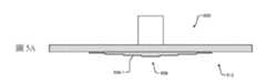
如圖5A、5B、以及5C所示,上電極500可包含設置成修改電漿分佈的其他示範下表面504-1、504-2、以及504-3(統稱為下表面504)。舉例而言,如圖5A所示,上電極500的下表面504-1可為台階狀或階梯狀。換言之,下表面504-1可具有從上電極500之中心區域508到該上電極之外區域512以台階方式減少的厚度。如圖5B所示,上電極500的下表面504-2可為彎曲狀(例如凸狀)。換言之,下表面504-2可具有從上電極500之中心區域508到該上電極之外區域512以曲線方式減少的厚度。如圖5C所示,下表面504-3可以片段直線方式形成斜向或傾斜。換言之,下表面504-3可具有從上電極500之中心區域508到該上電極之外區域512以不同角度減少及/或增加的厚度。例如,下表面504-3的厚度,在中心區域508中可以第一角度減少,在中內區域516中可以第二角度減少,在中外區域520中可以第三角度增加,以及在外區域512中可以第四角度減少。因此,可依照特定基板處理腔室中的電漿分佈特性來選擇與設置下表面504。在若干範例中,上電極500及下表面504的頂點與隅角可按照0.5 mm-10.0 mm的半徑加以磨圓。As shown in Figures 5A, 5B, and 5C,
如圖6A與6B所示,上電極600可包含設置成修改電漿分佈的其他示範下表面604-1與604-2(統稱為下表面604)。舉例而言,如圖6A所示,上電極600的下表面604-1,在中心區域608中可為彎曲狀(例如凸狀)以及在外區域612中可為凹狀。換言之,下表面604-1係從凸狀中心區域608轉變至凹狀外區域612,且中心區域608與凹狀區域612兩者在厚度上皆會變化。例如,下表面604-1可具有從中心區域608至外區域612中以曲線方式減少且然後從外區域612到邊緣區域616增加的厚度。在圖6A所示的邊緣區域616中,下表面604-1可為平坦。As shown in Figures 6A and 6B,
如圖6B所示,上電極600的下表面604-2,在中心區域608中可為漸縮(例如傾斜)以及在外區域612中可為凹狀。換言之,下表面604-2係從漸縮中心區域608轉變至凹狀外區域612,且中心區域608與凹狀區域612兩者在厚度上皆會變化。例如,下表面604-2可具有從中心區域608到外區域612中以直線方式減少且然後從外區域612到邊緣區域616增加的厚度。在圖6B所示的邊緣區域616中,下表面604-2可為凸狀、被形成圓角(radiused)、被磨圓等等。As shown in FIG. 6B , the lower surface 604 - 2 of the
先前描述在本質上僅為說明性的,而絕非意圖限制本揭露內容、其應用、或用途。本揭露內容之廣泛教示可以各種形式實施。因此,雖然本揭露內容包括特定範例,但由於當研究圖式、說明書、與以下申請專利範圍時,其他變化將變得顯而易見,故本揭露內容之真實範疇不應如此受限。應理解,在不改變本揭露內容之原理的情形下,方法中之一或更多步驟可以不同次序(或同時)執行。再者,雖然實施例之每一者係於以上描述為具有某些特徵,但關於本揭露內容之任何實施例所述該等特徵之任何一或更多者可在任何其他實施例中實施、及/或與其特徵組合(即使並未明確描述該組合)。換言之,所述實施例並非相互排斥,且一或更多實施例彼此的置換維持在本揭露內容之範疇中。The preceding description is merely illustrative in nature and is in no way intended to limit the disclosure, its application, or uses. The broad teachings of this disclosure can be implemented in a variety of forms. Therefore, while the disclosure includes specific examples, the true scope of the disclosure should not be so limited, since other variations will become apparent upon study of the drawings, specification, and scope of the following claims. It should be understood that one or more steps in the method may be performed in a different order (or simultaneously) without changing the principles of the present disclosure. Furthermore, although each of the embodiments is described above as having certain features, any one or more of those features described with respect to any embodiment of the present disclosure may be implemented in any other embodiment. and/or in combination with its characteristics (even if the combination is not explicitly described). In other words, the embodiments are not mutually exclusive, and substitutions of one or more embodiments for each other remain within the scope of the present disclosure.
元件 (例如,在模組、電路元件、半導體層等) 之間的空間與功能上的關係乃使用包括「連接」、「接合」、「耦合」、「鄰近」、「在…旁」、「在…之上」、「上方」、「下方」、與「設置」之各種術語描述。除非明確地描述為「直接」之情形下,否則當於上述揭露內容中描述第一與第二元件之間的關係時,該關係可為在第一與第二元件之間不存在其他中介元件之直接關係,但亦可為在第一與第二元件之間存在一或更多中介元件(空間上或功能上)的間接關係。如本文所用,詞組「A、B、與C之至少一者」應解釋成意指使用非排除性邏輯OR之邏輯(A OR B OR C),且不應解釋成代表「A之至少一者、B之至少一者、與C之至少一者」。Spatial and functional relationships between components (e.g., modules, circuit components, semiconductor layers, etc.) are defined using terms including "connected," "joined," "coupled," "adjacent," "next to," " Various terms describing "on", "above", "below", and "set". Unless explicitly described as "direct," when a relationship between a first and a second element is described in the above disclosure, the relationship may be such that there are no other intervening elements between the first and the second element. The relationship may be a direct relationship, but it may also be an indirect relationship where one or more intermediary elements (spatially or functionally) exist between the first and second elements. As used herein, the phrase "at least one of A, B, and C" shall be construed to mean the logic of OR using the non-exclusive logical OR (A OR B OR C), and shall not be construed to mean "at least one of A , at least one of B, and at least one of C."
在若干實施例中,控制器為系統的部分,該系統可為上述範例的部分。此種系統可包含半導體處理設備,其包含處理工具、腔室、處理用平台、及/或特定處理構件(晶圓基座、氣體流動系統等等)。這些系統可與電子元件整合在一起,該電子元件用以在處理半導體晶圓或基板之前、期間、以及之後,控制這些系統的操作。該電子元件可被稱為『控制器』,其可控制該系統的各種構件或子部件。可根據處理需求及/或系統類型,將該控制器程式化,以控制在此所揭露之任何處理,其包含處理氣體的輸送、溫度設定(例如,加熱及/或冷卻)、壓力設定、真空設定、功率設定、射頻(RF)產生器設定、RF匹配電路設定、頻率設定、流率設定、流體輸送設定、位置與操作設定、進入及離開與一特定系統連接或介接之一工具及其他搬運工具及/或負載室的晶圓搬運。In some embodiments, the controller is part of a system that may be part of the examples described above. Such systems may include semiconductor processing equipment, including processing tools, chambers, processing platforms, and/or specific processing components (wafer pedestals, gas flow systems, etc.). These systems may be integrated with electronics that are used to control the operation of these systems before, during, and after processing semiconductor wafers or substrates. This electronic component may be referred to as a "controller" that controls various components or subcomponents of the system. The controller can be programmed to control any of the processes disclosed herein, including process gas delivery, temperature settings (e.g., heating and/or cooling), pressure settings, vacuum, depending on process needs and/or system type. Settings, power settings, radio frequency (RF) generator settings, RF matching circuit settings, frequency settings, flow rate settings, fluid delivery settings, position and operation settings, entering and exiting a tool connected or interfaced with a specific system, and others Wafer handling by handling tools and/or load cells.
大體而言,該控制器可被定義為具有各種積體電路、邏輯、記憶體、及/或軟體的電子元件,其接收指令、發出指令、控制操作、進行清潔操作、進行終點測量等等。該積體電路可包含具有韌體形式而儲存有程式指令的晶片、數位信號處理器(DSP,digital signal processor)、被定義為特定用途積體電路(ASIC,application specific integrated circuits)的晶片、及/或一或多個微處理器、或執行程式指令(例如軟體)的微控制器。程式指令可為以各種獨立設定值(或程式檔案)形式傳送至控制器的指令,以定義用以在半導體晶圓上或對一系統實現特定處理的操作參數。在若干實施例中,這些操作參數可為製程工程師所定義之配方的部分,以在晶圓之一或多個層、材料、金屬、氧化物、矽、二氧化矽、表面、電路、及/或晶粒的加工期間實現一或多個處理步驟。Generally speaking, the controller can be defined as an electronic component with various integrated circuits, logic, memory, and/or software that receives instructions, issues instructions, controls operations, performs cleaning operations, performs endpoint measurements, and so on. The integrated circuit may include a chip having program instructions stored in firmware form, a digital signal processor (DSP), a chip defined as application specific integrated circuits (ASIC), and /or one or more microprocessors, or microcontrollers that execute program instructions (such as software). Program instructions may be instructions sent to the controller in the form of various independent settings (or program files) to define operating parameters for implementing specific processes on a semiconductor wafer or for a system. In some embodiments, these operating parameters may be part of a recipe defined by the process engineer to operate on one or more of the wafer's layers, materials, metals, oxides, silicon, silicon dioxide, surfaces, circuits, and/or or one or more processing steps are performed during processing of the die.
在若干實施例中,該控制器可為電腦的一部分或耦合至該電腦,該電腦係與該系統整合在一起,或耦合至該系統,或網路連接至該系統,或為其組合。例如,該控制器可位在「雲端(cloud)」中或為晶圓廠主電腦系統的全部或一部分,此可允許晶圓處理的遠端存取。該電腦可對該系統進行遠端存取,以監視加工操作的當前進度、檢查過去加工操作的歷史、從複數加工操作來檢查趨勢或性能指標、改變當前處理的參數、依當前處理來設定處理步驟、或開始新的處理。在若干範例中,遠端電腦(例如伺服器)可透過網路將處理配方提供給系統,該網路可包含區域網路或網際網路。該遠端電腦可包含使用者介面,其可進行參數及/或設定值的輸入或程式化,這些參數及/或設定值之後從該遠端電腦傳送至該系統。在若干範例中,該控制器接收具有資料形式的指令,該指令規定待於一或多個操作期間執行之每一處理步驟的參數。吾人應瞭解這些參數可特定於待執行之處理的類型以及該控制器所介接或控制之工具的類型。因此,如上所述,可以下列方式來分配該控制器:例如藉由包含以網路連接在一起並且為一共同目的(例如在此所述的處理與控制)而運作的一或多個分離控制器。為此種目的而分配的控制器之一範例可為在腔室上之一或多個積體電路,該積體電路係與遠端設置(例如平台等級或作為遠端電腦之部分)的一或多個積體電路通信,以聯合控制腔室上的處理。In some embodiments, the controller may be part of or coupled to a computer that is integrated with the system, coupled to the system, network connected to the system, or a combination thereof. For example, the controller could be located in the "cloud" or be all or part of the fab's main computer system, which could allow remote access to wafer processing. The computer can provide remote access to the system to monitor the current progress of machining operations, check the history of past machining operations, check trends or performance indicators from multiple machining operations, change parameters for the current process, and set processes based on the current process. step, or start a new process. In some examples, a remote computer (eg, a server) may provide processing recipes to the system over a network, which may include a local area network or the Internet. The remote computer may include a user interface that allows entry or programming of parameters and/or settings that are then transmitted from the remote computer to the system. In some examples, the controller receives instructions in the form of data that specify parameters for each processing step to be performed during one or more operations. It should be understood that these parameters may be specific to the type of processing to be performed and the type of tool that the controller interfaces with or controls. Thus, as noted above, the controller may be distributed in a manner such as by including one or more separate controllers that are networked together and operate for a common purpose (e.g., processing and control as described herein). device. An example of a controller assigned for this purpose could be one or more integrated circuits on the chamber that are part of a remote setup (e.g., platform level or as part of a remote computer). Or multiple integrated circuits communicate to jointly control processing on the chamber.
示範的系統可包含但不限於電漿蝕刻腔室或模組、沉積腔室或模組、旋轉清洗腔室或模組、金屬電鍍腔室或模組、清潔腔室或模組、斜邊蝕刻腔室或模組、物理氣相沉積(PVD)腔室或模組、化學氣相沉積(CVD)腔室或模組、原子層沉積(ALD)腔室或模組、原子層蝕刻(ALE,atomic layer etch)腔室或模組、離子植入腔室或模組、塗佈顯影(track)腔室或模組、以及可聯合或用於半導體晶圓之加工及/或製造的任何其他半導體處理系統。Exemplary systems may include, but are not limited to, plasma etching chambers or modules, deposition chambers or modules, spin cleaning chambers or modules, metal plating chambers or modules, cleaning chambers or modules, bevel etching Chamber or module, physical vapor deposition (PVD) chamber or module, chemical vapor deposition (CVD) chamber or module, atomic layer deposition (ALD) chamber or module, atomic layer etching (ALE, atomic layer etch) chamber or module, ion implantation chamber or module, coating and development (track) chamber or module, and any other semiconductor that can be combined with or used for the processing and/or manufacturing of semiconductor wafers processing system.
如上所述,根據待由該工具所執行的處理步驟,該控制器可與下列其中一或多者進行通信:其他工具電路或模組、其他工具構件、群集(cluster)工具、其他工具介面、相鄰工具、鄰近工具、設置遍布於工廠的工具、主電腦、另一控制器、或用於原料運送而將晶圓容器運至與運離半導體製造廠中之工具位置及/或裝載通道的工具。As noted above, depending on the processing steps to be performed by the tool, the controller may communicate with one or more of: other tool circuits or modules, other tool components, cluster tools, other tool interfaces, Adjacent tools, adjacent tools, tools located throughout the fab, a host computer, another controller, or tooling locations and/or loading lanes used for material transport to and from wafer containers in a semiconductor fabrication plant tool.
100:基板處理系統 102:處理腔室 104:上電極 106:基板支架 108:基板 109:噴淋頭 110:底板 112:陶瓷層 114:耐熱層 116:冷媒通道 118:邊緣環 120:RF產生系統 122:RF功率產生器 124:匹配與分佈網路 130:氣體輸送系統 132-1:氣體源 132-2:氣體源 132-N:氣體源 134-1:閥 134-N:閥 136-1:質量流量控制器 136-N:質量流量控制器 140:歧管 142:溫度控制器 144:加熱元件 146:冷媒組件 150:閥 152:幫浦 160:系統控制器 170:機器人 171:EFEM 172:承載室 173:VTM 176:保護密封件 180:電漿限制遮板 182:電漿區域 184:槽孔 186:氣溶膠輸送系統 200:基板處理腔室 204:基板支架 208:氣體分佈裝置 212:底板 216:上電極 220:內電極 224:外電極 228:陶瓷層 232:基板 236:接合層 240:保護密封件 242:邊緣環 244:電漿限制遮板 248:處理容積 252:下表面 260:中心尖峰 264:外尖峰 300:基板處理腔室 304:基板支架 308:氣體分佈裝置 312:底板 316:上電極 320:內電極 324:外電極 328:陶瓷層 332:基板 336:接合層 340:保護密封件 342:邊緣環 344:電漿限制遮板 348:處理容積 352:下表面 356:第一部分 360:第二部分 364:中心 372:中心區域 376:外區域 380:頂點 400:基板處理腔室 404:基板支架 408:氣體分佈裝置 412:底板 416:上電極 420:內電極 424:外電極 428:陶瓷層 432:基板 436:接合層 440:保護密封件 442:邊緣環 444:電漿限制遮板 448:處理容積 452:下表面 456:第一部分 460:第二部分 464:中心 472:中心區域 476:外區域 480:頂點 500:上電極 504-1:下表面 504-2:下表面 504-3:下表面 508:中心區域 512:外區域 516:中內區域 520:中外區域 600:上電極 604-1:下表面 604-2:下表面 608:中心區域 612:外區域 616:邊緣區域100:Substrate processing system 102: Processing chamber 104: Upper electrode 106:Substrate bracket 108:Substrate 109:Sprinkler head 110: Bottom plate 112:Ceramic layer 114: Heat-resistant layer 116:Refrigerant channel 118: Edge ring 120:RF generation system 122:RF power generator 124: Matching and Distribution Networks 130:Gas delivery system 132-1:Gas source 132-2:Gas source 132-N:Gas source 134-1:Valve 134-N:Valve 136-1:Mass flow controller 136-N:Mass flow controller 140:Manifold 142: Temperature controller 144:Heating element 146:Refrigerant components 150: valve 152:Pump 160:System controller 170:Robot 171:EFEM 172: Bearing room 173:VTM 176: Protective seals 180: Plasma confinement shutter 182:Plasma area 184:Slot 186:Aerosol delivery system 200: Substrate processing chamber 204:Substrate bracket 208:Gas distribution device 212: Base plate 216: Upper electrode 220:Internal electrode 224:External electrode 228:Ceramic layer 232:Substrate 236:Jointing layer 240: Protective seals 242: Edge ring 244: Plasma confinement shutter 248: processing volume 252: Lower surface 260: Center spike 264:Outer spike 300: Substrate processing chamber 304:Substrate bracket 308:Gas distribution device 312: Base plate 316: Upper electrode 320:Internal electrode 324:External electrode 328:Ceramic layer 332:Substrate 336:Jointing layer 340: Protective seals 342: Edge ring 344: Plasma confinement shutter 348:Processing volume 352: Lower surface 356:Part One 360:Part 2 364:center 372:Central area 376:Outer area 380: vertex 400: Substrate processing chamber 404:Substrate bracket 408:Gas distribution device 412: Base plate 416: Upper electrode 420:Internal electrode 424:External electrode 428:Ceramic layer 432:Substrate 436:Jointing layer 440: Protective seals 442: Edge ring 444: Plasma confinement shutter 448:Processing volume 452: Lower surface 456:Part One 460:Part 2 464:Center 472:Central area 476:Outer area 480: vertex 500: Upper electrode 504-1: Lower surface 504-2: Lower surface 504-3: Lower surface 508:Central area 512:Outer area 516:Central area 520:Chinese and foreign regions 600: Upper electrode 604-1: Lower surface 604-2: Lower surface 608:Central area 612:Outer area 616: Edge area
本揭露內容將由詳細說明與附圖而變得更受到完整瞭解,其中:This disclosure will be more fully understood by the detailed description and accompanying drawings, in which:
圖1係依照本揭露內容之原理的一示範基板處理系統;Figure 1 is an exemplary substrate processing system in accordance with the principles of the present disclosure;
圖2係一示範基板處理腔室;Figure 2 is a demonstration substrate processing chamber;
圖3係依照本揭露內容之原理的一基板處理腔室,該基板處理腔室包含一示範上電極;FIG. 3 illustrates a substrate processing chamber including an exemplary upper electrode in accordance with principles of the present disclosure;
圖4係依照本揭露內容之原理的一基板處理腔室,該基板處理腔室包含另一示範上電極;以及Figure 4 is a substrate processing chamber including another exemplary upper electrode in accordance with principles of the present disclosure; and
圖5A、5B、以及5C係依照本揭露內容之原理的示範上電極。Figures 5A, 5B, and 5C are exemplary top electrodes in accordance with the principles of the present disclosure.
圖6A與6B係依照本揭露內容之原理的示範上電極。Figures 6A and 6B are exemplary top electrodes in accordance with the principles of the present disclosure.
在圖式中,參考符號可重複使用以指示相似及/或相同的元件。In the drawings, reference symbols may be used repeatedly to indicate similar and/or identical elements.
600:上電極600: Upper electrode
604-1:下表面604-1: Lower surface
608:中心區域608:Central area
612:外區域612:Outer area
616:邊緣區域616: Edge area
Claims (10)
Translated fromChineseApplications Claiming Priority (2)
| Application Number | Priority Date | Filing Date | Title |
|---|---|---|---|
| US15/888,719US20190244793A1 (en) | 2018-02-05 | 2018-02-05 | Tapered upper electrode for uniformity control in plasma processing |
| US15/888,719 | 2018-02-05 |
Publications (2)
| Publication Number | Publication Date |
|---|---|
| TW202316521A TW202316521A (en) | 2023-04-16 |
| TWI835453Btrue TWI835453B (en) | 2024-03-11 |
Family
ID=67476986
Family Applications (3)
| Application Number | Title | Priority Date | Filing Date |
|---|---|---|---|
| TW111146973ATWI835453B (en) | 2018-02-05 | 2019-01-28 | Tapered upper electrode for uniformity control in plasma processing |
| TW111111827ATWI802347B (en) | 2018-02-05 | 2019-01-28 | Tapered upper electrode for uniformity control in plasma processing |
| TW108103024ATWI763969B (en) | 2018-02-05 | 2019-01-28 | Tapered upper electrode for uniformity control in plasma processing |
Family Applications After (2)
| Application Number | Title | Priority Date | Filing Date |
|---|---|---|---|
| TW111111827ATWI802347B (en) | 2018-02-05 | 2019-01-28 | Tapered upper electrode for uniformity control in plasma processing |
| TW108103024ATWI763969B (en) | 2018-02-05 | 2019-01-28 | Tapered upper electrode for uniformity control in plasma processing |
Country Status (4)
| Country | Link |
|---|---|
| US (1) | US20190244793A1 (en) |
| KR (8) | KR102035960B1 (en) |
| CN (1) | CN110277293A (en) |
| TW (3) | TWI835453B (en) |
Families Citing this family (22)
| Publication number | Priority date | Publication date | Assignee | Title |
|---|---|---|---|---|
| US20190244793A1 (en)* | 2018-02-05 | 2019-08-08 | Lam Research Corporation | Tapered upper electrode for uniformity control in plasma processing |
| US11335539B2 (en)* | 2018-09-28 | 2022-05-17 | Lam Research Corporation | Systems and methods for optimizing power delivery to an electrode of a plasma chamber |
| US20210287881A1 (en)* | 2020-03-12 | 2021-09-16 | Applied Materials, Inc. | Methods and apparatus for tuning semiconductor processes |
| CN111370287B (en)* | 2020-03-24 | 2025-06-10 | 长江存储科技有限责任公司 | Upper electrode device and plasma processing device |
| WO2021257462A1 (en)* | 2020-06-15 | 2021-12-23 | Lam Research Corporation | Showerhead faceplates with angled gas distribution passages for semiconductor processing tools |
| KR102793905B1 (en)* | 2020-08-14 | 2025-04-08 | 삼성전자주식회사 | Upper electrode and substrate processing apparatus including the same |
| JP7489896B2 (en)* | 2020-10-22 | 2024-05-24 | 東京エレクトロン株式会社 | Plasma Processing Equipment |
| KR102841826B1 (en) | 2020-12-16 | 2025-08-04 | 삼성전자주식회사 | Semiconductor processing equipment including electrostatic chuck for plasma processing |
| KR102583263B1 (en)* | 2020-12-30 | 2023-10-04 | 세메스 주식회사 | Substrate treating apparatus |
| EP4292118A4 (en)* | 2021-02-12 | 2025-01-22 | LAM Research Corporation | C-SHOULDER MODIFICATION FOR PLASMA UNIFORMITY WITHOUT IMPACT ON C-SHOULDER MECHANICAL STRENGTH OR LIFE |
| US12338530B2 (en) | 2021-07-09 | 2025-06-24 | Applied Materials, Inc. | Shaped showerhead for edge plasma modulation |
| KR102766433B1 (en)* | 2022-08-30 | 2025-02-13 | 주식회사 케이씨파츠텍 | Modular profiled upper electrode and plasma processing apparatus therewith |
| WO2023043091A1 (en)* | 2021-09-14 | 2023-03-23 | 주식회사 티이엠 | Assembly-type profile upper electrode and plasma processing apparatus including same |
| KR102617128B1 (en)* | 2021-09-14 | 2023-12-27 | 주식회사 케이씨파츠텍 | Modular profiled upper electrode and plasma processing apparatus therewith |
| CN114203513A (en)* | 2021-12-14 | 2022-03-18 | 拓荆科技股份有限公司 | Power electrode and plasma processing equipment |
| KR102426136B1 (en)* | 2022-03-14 | 2022-07-27 | (주)코마테크놀로지 | Upper electrode processing method for etching having a curved surface and variable thickness using electrode for discharge processing |
| CN114727464B (en)* | 2022-03-29 | 2023-03-24 | 电子科技大学 | Method for prolonging service life of plasma spheroidization radio frequency torch and radio frequency torch |
| CN119836673A (en)* | 2022-09-07 | 2025-04-15 | 朗姆研究公司 | Shaped silicon external upper electrode for plasma treatment |
| JP7460858B1 (en)* | 2023-04-26 | 2024-04-02 | エスケー エンパルス カンパニー リミテッド | Upper electrode, semiconductor device manufacturing apparatus including the same, and semiconductor device manufacturing method |
| KR102615786B1 (en)* | 2023-04-26 | 2023-12-19 | 에스케이엔펄스 주식회사 | upper elelctrode, semiconductor device manufacturing apparatus including the same and manufacturing method for semiconductor device |
| KR102615787B1 (en)* | 2023-04-26 | 2023-12-19 | 에스케이엔펄스 주식회사 | upper elelctrode, semiconductor device manufacturing apparatus including the same and manufacturing method for semiconductor device |
| KR102611375B1 (en)* | 2023-04-26 | 2023-12-06 | 에스케이엔펄스 주식회사 | upper elelctrode, semiconductor device manufacturing apparatus including the same and manufacturing method for semiconductor device |
Citations (4)
| Publication number | Priority date | Publication date | Assignee | Title |
|---|---|---|---|---|
| US20030089314A1 (en)* | 1999-03-18 | 2003-05-15 | Nobuo Matsuki | Plasma CVD film-forming device |
| US20070227666A1 (en)* | 2006-03-30 | 2007-10-04 | Tokyo Electron Limited | Plasma processing apparatus |
| US20090269512A1 (en)* | 2008-04-28 | 2009-10-29 | Applied Materials, Inc. | Nonplanar faceplate for a plasma processing chamber |
| WO2009154889A2 (en)* | 2008-06-20 | 2009-12-23 | Applied Materials, Inc. | Gas distribution showerhead skirt |
Family Cites Families (23)
| Publication number | Priority date | Publication date | Assignee | Title |
|---|---|---|---|---|
| KR100252210B1 (en)* | 1996-12-24 | 2000-04-15 | 윤종용 | Dry etching facility for manufacturing semiconductor devices |
| JP2001267305A (en)* | 2000-03-17 | 2001-09-28 | Hitachi Ltd | Plasma processing equipment |
| US6391787B1 (en)* | 2000-10-13 | 2002-05-21 | Lam Research Corporation | Stepped upper electrode for plasma processing uniformity |
| JP4047616B2 (en)* | 2002-04-03 | 2008-02-13 | 東京エレクトロン株式会社 | Plasma processing apparatus and plasma processing method |
| KR20050013734A (en)* | 2003-07-29 | 2005-02-05 | 삼성전자주식회사 | Plasma Etching Apparatus |
| DE602004007017T2 (en)* | 2003-09-10 | 2008-02-07 | Oc Oerlikon Balzers Ag | VOLTAGE DENSITY COMPENSATION METHOD FOR A HIGH FREQUENCY PLASMA RETRACTOR FOR TREATING RECTANGULAR LARGE SUBSTRATE |
| FR2884044A1 (en)* | 2005-04-01 | 2006-10-06 | St Microelectronics Sa | Reactor for the deposition of an oxide layer on a platelet, notably for the deposition of tantalum pentoxide during the fabrication of integrated circuits |
| JP4707588B2 (en)* | 2006-03-16 | 2011-06-22 | 東京エレクトロン株式会社 | Plasma processing apparatus and electrodes used therefor |
| KR101264695B1 (en)* | 2006-09-01 | 2013-05-16 | 엘지디스플레이 주식회사 | Apparatus for plasma enhanced chemical vapor deposition |
| US7829815B2 (en)* | 2006-09-22 | 2010-11-09 | Taiwan Semiconductor Manufacturing Co., Ltd. | Adjustable electrodes and coils for plasma density distribution control |
| US8435379B2 (en)* | 2007-05-08 | 2013-05-07 | Applied Materials, Inc. | Substrate cleaning chamber and cleaning and conditioning methods |
| DE102007028293B4 (en)* | 2007-06-20 | 2009-09-03 | Universität Augsburg | Plasma reactor, its use and process for producing monocrystalline diamond films |
| EP2195820B1 (en)* | 2007-10-01 | 2014-12-31 | TEL Solar AG | Deposition of active films |
| KR20090044420A (en)* | 2007-10-31 | 2009-05-07 | 주식회사 하이닉스반도체 | Plasma processing equipment for semiconductor device manufacturing |
| KR101094976B1 (en)* | 2008-02-08 | 2011-12-20 | 도쿄엘렉트론가부시키가이샤 | Plasma processing equipment |
| US9177761B2 (en)* | 2009-08-25 | 2015-11-03 | Semiconductor Energy Laboratory Co., Ltd. | Plasma CVD apparatus, method for forming microcrystalline semiconductor film and method for manufacturing semiconductor device |
| KR101112745B1 (en)* | 2010-02-02 | 2012-02-24 | 위순임 | Plasma reactor have a variable capacitively coupled plasma |
| US8617350B2 (en)* | 2011-06-15 | 2013-12-31 | Belight Technology Corporation, Limited | Linear plasma system |
| US20140299273A1 (en)* | 2013-04-08 | 2014-10-09 | Lam Research Corporation | Multi-segment electrode assembly and methods therefor |
| KR20150057095A (en)* | 2013-11-18 | 2015-05-28 | 주성엔지니어링(주) | Electrode for plasma generation and apparatus for plasma processing including the same |
| JP2016184610A (en)* | 2015-03-25 | 2016-10-20 | 株式会社東芝 | Upper electrode, edge ring and plasma processing apparatus |
| CN104835712A (en)* | 2015-03-25 | 2015-08-12 | 沈阳拓荆科技有限公司 | Cambered surface spraying head applied to semiconductor plasma processing device |
| US20190244793A1 (en)* | 2018-02-05 | 2019-08-08 | Lam Research Corporation | Tapered upper electrode for uniformity control in plasma processing |
- 2018
- 2018-02-05USUS15/888,719patent/US20190244793A1/enactivePending
- 2019
- 2019-01-21KRKR1020190007436Apatent/KR102035960B1/enactiveActive
- 2019-01-28TWTW111146973Apatent/TWI835453B/enactive
- 2019-01-28TWTW111111827Apatent/TWI802347B/enactive
- 2019-01-28TWTW108103024Apatent/TWI763969B/enactive
- 2019-02-02CNCN201910106940.1Apatent/CN110277293A/enactivePending
- 2019-10-17KRKR1020190129191Apatent/KR102236832B1/enactiveActive
- 2021
- 2021-03-31KRKR1020210041999Apatent/KR102275987B1/enactiveActive
- 2021-07-06KRKR1020210088189Apatent/KR102378582B1/enactiveActive
- 2022
- 2022-03-21KRKR1020220034841Apatent/KR102451669B1/enactiveActive
- 2022-09-30KRKR1020220125403Apatent/KR102556016B1/enactiveActive
- 2023
- 2023-07-11KRKR1020230089976Apatent/KR102838302B1/enactiveActive
- 2025
- 2025-07-21KRKR1020250098359Apatent/KR20250116612A/enactivePending
Patent Citations (4)
| Publication number | Priority date | Publication date | Assignee | Title |
|---|---|---|---|---|
| US20030089314A1 (en)* | 1999-03-18 | 2003-05-15 | Nobuo Matsuki | Plasma CVD film-forming device |
| US20070227666A1 (en)* | 2006-03-30 | 2007-10-04 | Tokyo Electron Limited | Plasma processing apparatus |
| US20090269512A1 (en)* | 2008-04-28 | 2009-10-29 | Applied Materials, Inc. | Nonplanar faceplate for a plasma processing chamber |
| WO2009154889A2 (en)* | 2008-06-20 | 2009-12-23 | Applied Materials, Inc. | Gas distribution showerhead skirt |
Also Published As
| Publication number | Publication date |
|---|---|
| US20190244793A1 (en) | 2019-08-08 |
| KR20190120741A (en) | 2019-10-24 |
| KR102275987B9 (en) | 2025-08-26 |
| KR102451669B1 (en) | 2022-10-06 |
| KR20210040337A (en) | 2021-04-13 |
| TW202228205A (en) | 2022-07-16 |
| KR20250116612A (en) | 2025-08-01 |
| KR102451669B9 (en) | 2025-08-26 |
| KR20210089121A (en) | 2021-07-15 |
| KR102236832B9 (en) | 2025-08-26 |
| KR102035960B1 (en) | 2019-10-23 |
| TW201941298A (en) | 2019-10-16 |
| TWI763969B (en) | 2022-05-11 |
| KR102838302B1 (en) | 2025-07-23 |
| KR102838302B9 (en) | 2025-08-26 |
| KR102556016B9 (en) | 2025-08-26 |
| TW202316521A (en) | 2023-04-16 |
| KR20220138849A (en) | 2022-10-13 |
| KR20220042082A (en) | 2022-04-04 |
| KR102378582B1 (en) | 2022-03-23 |
| TWI802347B (en) | 2023-05-11 |
| KR20230112093A (en) | 2023-07-26 |
| CN110277293A (en) | 2019-09-24 |
| KR20190095117A (en) | 2019-08-14 |
| KR102378582B9 (en) | 2025-08-26 |
| KR102275987B1 (en) | 2021-07-13 |
| KR102556016B1 (en) | 2023-07-13 |
| KR102236832B1 (en) | 2021-04-06 |
Similar Documents
| Publication | Publication Date | Title |
|---|---|---|
| TWI835453B (en) | Tapered upper electrode for uniformity control in plasma processing | |
| KR102488729B1 (en) | Control of on-wafer cd uniformity with movable edge ring and gas injection adjustment | |
| CN110383454B (en) | Bottom edge ring and middle edge ring | |
| KR102454532B1 (en) | Electrostatic chuck with features for preventing electrical arcing and light-up and improving process uniformity | |
| KR102800602B1 (en) | Limited ring with extended life | |
| KR102521717B1 (en) | Helium plug design to reduce arcing | |
| KR102800597B1 (en) | Edge ring focused deposition during cleaning process in processing chamber | |
| KR102430432B1 (en) | Planar substrate edge contact with open volume equalization pathways and side containment | |
| US20230369091A1 (en) | High temperature pedestal with extended electrostatic chuck electrode | |
| KR20220160073A (en) | Plasma-exclusion-zone rings for processing notched wafers | |
| TWI849145B (en) | Reduced diameter carrier ring hardware for substrate processing systems | |
| TW202507918A (en) | Bottom and middle edge rings |