TWI832395B - Assembly type light emitting diode display device - Google Patents
Assembly type light emitting diode display deviceDownload PDFInfo
- Publication number
- TWI832395B TWI832395BTW111132112ATW111132112ATWI832395BTW I832395 BTWI832395 BTW I832395BTW 111132112 ATW111132112 ATW 111132112ATW 111132112 ATW111132112 ATW 111132112ATW I832395 BTWI832395 BTW I832395B
- Authority
- TW
- Taiwan
- Prior art keywords
- light
- emitting diode
- electrically connected
- assembled
- emitting diodes
- Prior art date
Links
- 239000000758substrateSubstances0.000claimsabstractdescription42
- 239000003086colorantSubstances0.000claimsdescription7
- 239000004642PolyimideSubstances0.000claimsdescription5
- XUIMIQQOPSSXEZ-UHFFFAOYSA-NSiliconChemical compound[Si]XUIMIQQOPSSXEZ-UHFFFAOYSA-N0.000claimsdescription5
- 239000011521glassSubstances0.000claimsdescription5
- 229920001721polyimidePolymers0.000claimsdescription5
- 229910052710siliconInorganic materials0.000claimsdescription5
- 239000010703siliconSubstances0.000claimsdescription5
- 238000000034methodMethods0.000description17
- 239000000463materialSubstances0.000description7
- 239000010409thin filmSubstances0.000description6
- 230000000694effectsEffects0.000description5
- 235000012431wafersNutrition0.000description2
- 229910021417amorphous siliconInorganic materials0.000description1
- 238000006243chemical reactionMethods0.000description1
- 230000005669field effectEffects0.000description1
- 230000020169heat generationEffects0.000description1
- 238000012986modificationMethods0.000description1
- 230000004048modificationEffects0.000description1
- 230000003071parasitic effectEffects0.000description1
- 229910021420polycrystalline siliconInorganic materials0.000description1
- 239000002096quantum dotSubstances0.000description1
- 239000004065semiconductorSubstances0.000description1
Images


Classifications
- G—PHYSICS
- G09—EDUCATION; CRYPTOGRAPHY; DISPLAY; ADVERTISING; SEALS
- G09G—ARRANGEMENTS OR CIRCUITS FOR CONTROL OF INDICATING DEVICES USING STATIC MEANS TO PRESENT VARIABLE INFORMATION
- G09G3/00—Control arrangements or circuits, of interest only in connection with visual indicators other than cathode-ray tubes
- G09G3/20—Control arrangements or circuits, of interest only in connection with visual indicators other than cathode-ray tubes for presentation of an assembly of a number of characters, e.g. a page, by composing the assembly by combination of individual elements arranged in a matrix no fixed position being assigned to or needed to be assigned to the individual characters or partial characters
- G09G3/22—Control arrangements or circuits, of interest only in connection with visual indicators other than cathode-ray tubes for presentation of an assembly of a number of characters, e.g. a page, by composing the assembly by combination of individual elements arranged in a matrix no fixed position being assigned to or needed to be assigned to the individual characters or partial characters using controlled light sources
- G09G3/30—Control arrangements or circuits, of interest only in connection with visual indicators other than cathode-ray tubes for presentation of an assembly of a number of characters, e.g. a page, by composing the assembly by combination of individual elements arranged in a matrix no fixed position being assigned to or needed to be assigned to the individual characters or partial characters using controlled light sources using electroluminescent panels
- G09G3/32—Control arrangements or circuits, of interest only in connection with visual indicators other than cathode-ray tubes for presentation of an assembly of a number of characters, e.g. a page, by composing the assembly by combination of individual elements arranged in a matrix no fixed position being assigned to or needed to be assigned to the individual characters or partial characters using controlled light sources using electroluminescent panels semiconductive, e.g. using light-emitting diodes [LED]
- H—ELECTRICITY
- H01—ELECTRIC ELEMENTS
- H01L—SEMICONDUCTOR DEVICES NOT COVERED BY CLASS H10
- H01L25/00—Assemblies consisting of a plurality of semiconductor or other solid state devices
- H01L25/16—Assemblies consisting of a plurality of semiconductor or other solid state devices the devices being of types provided for in two or more different subclasses of H10B, H10D, H10F, H10H, H10K or H10N, e.g. forming hybrid circuits
- H01L25/167—Assemblies consisting of a plurality of semiconductor or other solid state devices the devices being of types provided for in two or more different subclasses of H10B, H10D, H10F, H10H, H10K or H10N, e.g. forming hybrid circuits comprising optoelectronic devices, e.g. LED, photodiodes
- G—PHYSICS
- G09—EDUCATION; CRYPTOGRAPHY; DISPLAY; ADVERTISING; SEALS
- G09F—DISPLAYING; ADVERTISING; SIGNS; LABELS OR NAME-PLATES; SEALS
- G09F9/00—Indicating arrangements for variable information in which the information is built-up on a support by selection or combination of individual elements
- G09F9/30—Indicating arrangements for variable information in which the information is built-up on a support by selection or combination of individual elements in which the desired character or characters are formed by combining individual elements
- G09F9/33—Indicating arrangements for variable information in which the information is built-up on a support by selection or combination of individual elements in which the desired character or characters are formed by combining individual elements being semiconductor devices, e.g. diodes
- G—PHYSICS
- G09—EDUCATION; CRYPTOGRAPHY; DISPLAY; ADVERTISING; SEALS
- G09G—ARRANGEMENTS OR CIRCUITS FOR CONTROL OF INDICATING DEVICES USING STATIC MEANS TO PRESENT VARIABLE INFORMATION
- G09G2300/00—Aspects of the constitution of display devices
- G09G2300/04—Structural and physical details of display devices
- G09G2300/0421—Structural details of the set of electrodes
- G09G2300/0426—Layout of electrodes and connections
- H—ELECTRICITY
- H01—ELECTRIC ELEMENTS
- H01L—SEMICONDUCTOR DEVICES NOT COVERED BY CLASS H10
- H01L25/00—Assemblies consisting of a plurality of semiconductor or other solid state devices
- H01L25/16—Assemblies consisting of a plurality of semiconductor or other solid state devices the devices being of types provided for in two or more different subclasses of H10B, H10D, H10F, H10H, H10K or H10N, e.g. forming hybrid circuits
- H01L25/162—Assemblies consisting of a plurality of semiconductor or other solid state devices the devices being of types provided for in two or more different subclasses of H10B, H10D, H10F, H10H, H10K or H10N, e.g. forming hybrid circuits the devices being mounted on two or more different substrates
Landscapes
- Engineering & Computer Science (AREA)
- Microelectronics & Electronic Packaging (AREA)
- Physics & Mathematics (AREA)
- General Physics & Mathematics (AREA)
- Computer Hardware Design (AREA)
- Condensed Matter Physics & Semiconductors (AREA)
- Power Engineering (AREA)
- Theoretical Computer Science (AREA)
- Devices For Indicating Variable Information By Combining Individual Elements (AREA)
- Control Of Indicators Other Than Cathode Ray Tubes (AREA)
- Led Devices (AREA)
Abstract
Translated fromChineseDescription
Translated fromChinese本發明是有關於一種發光二極體顯示裝置,特別是指一種組裝型態的發光二極體顯示裝置。The present invention relates to a light-emitting diode display device, and in particular, to an assembled type light-emitting diode display device.
發光二極體(LED),尤其是微型發光二極體(例如mini-LED或Micro-LED),由於具有體積小、高亮度、發熱量低,以及省電等優點,近年來已廣泛應用於不同領域且已成為照明及光源的主流。然而,當需要使用大量的發光二極體,例如,將發光二極體應用於顯示器的顯示光源時,也因為其尺寸的微型化及應用時所需的巨額數量,不僅轉移過程耗時也容易造成轉移對位的公差問題,使得巨量轉移成為目前發微型發光二極體於商業化應用的一個重要瓶頸。Light-emitting diodes (LEDs), especially micro-LEDs (such as mini-LED or Micro-LED), have been widely used in recent years due to their advantages such as small size, high brightness, low heat generation, and power saving. Different fields and has become the mainstream of lighting and light sources. However, when a large number of light-emitting diodes need to be used, for example, when light-emitting diodes are applied to the display light source of a display, due to the miniaturization of their size and the huge amount required for application, the transfer process is not only time-consuming but also easy to The tolerance problem caused by transfer alignment makes mass transfer an important bottleneck in the current commercial application of micro-light-emitting diodes.
因此,本發明的目的,即在提供一種減少巨量轉移良率不足的組裝型發光二極體顯示裝置。Therefore, an object of the present invention is to provide an assembled light-emitting diode display device that reduces the yield problem of mass transfer.
於是,本發明的組裝型發光二極體顯示裝置,包含一系統母板,及多個組裝子板。Therefore, the assembled light-emitting diode display device of the present invention includes a system motherboard and a plurality of assembled daughter boards.
該系統母板具有一驅動電源電路單元、一閘極控制電路單元。The system motherboard has a driving power circuit unit and a gate control circuit unit.
該等組裝子板設置於該系統母板,每一個組裝子板具有一基板、至少兩組設置於該基板的發光二極體單元,及至少一電晶體開關,每一組發光二極體單元具有多個發光二極體,且同一組發光二極體單元的發光二極體與相同的該電晶體開關電連接。The assembled daughter boards are arranged on the system motherboard. Each assembled daughter board has a substrate, at least two groups of light emitting diode units arranged on the substrate, and at least one transistor switch. Each group of light emitting diode units There are multiple light-emitting diodes, and the light-emitting diodes of the same group of light-emitting diode units are electrically connected to the same transistor switch.
其中,該等發光二極體於該系統母板上成行列間隔排列,該驅動電源電路單元具有多條沿一第一方向同向延伸的電源線,該閘極控制電路單元具有多條沿一與該第一方向相交的第二方向延伸的閘極線,位於同一條沿該第一方向排列的發光二極體與相應的一條電源線電連接,且位於同一組裝子板的至少一電晶體開關的閘極與同一條閘極線電連接,以接收時序訊號。Wherein, the light-emitting diodes are arranged in rows and columns on the system motherboard, the driving power circuit unit has a plurality of power lines extending in the same direction along a first direction, and the gate control circuit unit has a plurality of power lines extending along a first direction. The gate line extending in the second direction intersecting the first direction is located on the same light-emitting diode arranged along the first direction and is electrically connected to a corresponding power line, and is located on at least one transistor of the same assembly sub-board. The gate of the switch is electrically connected to the same gate line to receive timing signals.
本發明的功效在於:利用組裝方式,將多個預先設有多數發光二極體及至少一個電晶體開關的組裝子板,以組裝方式裝設至一系統母板,而可藉由組裝子板同時轉移大量的發光二極體以減少巨量轉移的問題。The effect of the present invention is to use an assembly method to install a plurality of assembly daughter boards pre-installed with a plurality of light-emitting diodes and at least one transistor switch on a system motherboard, and by assembling the daughter boards Transfer a large number of light-emitting diodes at the same time to reduce the problem of mass transfer.
20:系統母板20:System motherboard
21:板體21:Plate body
22:時序控制單元22: Timing control unit
23:驅動電源電路單元23: Drive power circuit unit
231:驅動IC231:Driver IC
232:電源線232:Power cord
24:閘極控制電路單元24: Gate control circuit unit
241:閘極訊號控制器241: Gate signal controller
G:閘極線G: Gate line
25:接地線路25:Ground line
30:組裝子板30:Assemble the daughter board
31:基板31:Substrate
32:發光二極體單元32:LED unit
L:發光二極體L: light emitting diode
R、G、B:紅光、綠光、藍光發光二極體R, G, B: red, green, blue light-emitting diodes
T:電晶體開關T: transistor switch
Y:第一方向Y: first direction
X:第二方向X: second direction
V:正電壓源V: Positive voltage source
本發明的其他的特徵及功效,將於參照圖式的實施方式中清楚地呈現,其中:圖1是一俯視示意圖,說明本發明組裝型發光二極體顯示裝置的一實施例;圖2是一俯視示意圖,輔助說明圖1該實施例的其中一組裝子板的發光顯示單元;圖3是一俯視示意圖,說明該實施例的該等發光顯示單元與電晶體開關的另一電連接態樣;圖4是一俯視示意圖,說明該實施例的該等發光顯示單元與電晶體開關的另一實施態樣;及圖5是一俯視示意圖,說明該實施例的其中一組裝子板的發光顯示單元的發光二極體數量及排列方式的另一態樣。Other features and effects of the present invention will be clearly presented in the embodiments with reference to the drawings, in which: Figure 1 is a schematic top view illustrating an embodiment of the assembled light-emitting diode display device of the present invention; Figure 2 is a A schematic top view to assist in explaining the light-emitting display unit of one of the assembled sub-boards in the embodiment of Figure 1; Figure 3 is a schematic top view to illustrate another electrical connection between the light-emitting display units and the transistor switch in this embodiment. ; Figure 4 is a schematic top view illustrating another implementation of the light-emitting display units and transistor switches of this embodiment; and Figure 5 is a top schematic view illustrating the light-emitting display of one of the assembled sub-boards of this embodiment Another aspect of the number and arrangement of the light-emitting diodes of the unit.
有關本發明之相關技術內容、特點與功效,在以下配合參考圖式之實施例的詳細說明中,將可清楚的呈現。此外,要說明的是,本發明圖式僅為表示元件間的結構及/或位置相對關係,與各元件的實際尺寸並不相關。The relevant technical contents, features and effects of the present invention will be clearly presented in the following detailed description of the embodiments with reference to the drawings. In addition, it should be noted that the drawings of the present invention only represent the relative structure and/or positional relationship between components, and are not related to the actual size of each component.
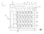
參閱圖1、2,本發明組裝型發光二極體顯示裝置的一實施例,包含一系統母板20,及多個組裝子板30。Referring to FIGS. 1 and 2 , an embodiment of the assembled light-emitting diode display device of the present invention includes a
該系統母板20包括一板體21、設置於該板體21的一時序控制單元22,及分別與該時序控制單元22電連接的一驅動電源電路單元23、一閘極控制電路單元24,及一接地線路25。The
詳細的說,該板體21可以是玻璃基板、矽基板、聚醯亞胺(Polyimide,PI),或電路板等,於本實施例中該板體21是以具有電路結構的電路板為例說明。該時序控制單元22設置於該板體21並與該電路結構電連接,可用於分別提供時序訊號至該驅動電源電路單元23及該閘極控制電路單元24。該驅動電源電路單元23具有一與該時序控制單元22電連接的驅動IC231,及多條分別與該驅動IC231電連接的電源線232。該等電源線232彼此交錯間隔且沿一第一方向Y同向延伸,該驅動IC231可接收時序訊號並控制提供至該等電源線232的驅動電流。該閘極控制電路單元24具有一與該時序控制單元22電連接的一閘極訊號控制器241,及多條分別與該閘極訊號控制器241電連接的閘極線G,該等閘極線G沿一垂直該第一方向Y的第二方向X同向延伸。於本實施例中,是以該第一方向為Y方向,該第二方向為X方向為例說明,然實際實施時並不以此為限。Specifically, the
該等組裝子板30組設於該系統母板20上。每一個組裝子板30具有一面積小於該系統母板20之板體21的基板31、多組設置於該基板31的發光二極體單元32,及一個電晶體開關T。The
該基板31可以是玻璃基板、矽基板、聚醯亞胺,或電路板等。每一組發光二極體單元32具有3個可發出3種不同色光,圖1以R、B、G分別表示可發出紅光、藍光、綠光的發光二極體L,且該電晶體開關T同時與該等發光二極體單元32的每一個發光二極體L電連接。The
該等發光二極體L可以是一般尺寸(長x寬尺寸不大於100μm),或是尺寸更小的mini-LED或micro LED(長x寬尺寸不大於20μm)。該電晶體開關T為場效電晶體(Field-Effect Transistor,FET)。例如該電晶體開關T可以是薄膜電晶體(Thin-Film Transistor,TFT),並可透過半導體製程直接形成於該基板31,此外,該電晶體開關T會配合該基板31的材料而為N型電晶體或P型電晶體。舉例來說,若該基板31為玻璃基板,沉積於其表面的材料為非晶矽(Amorphous,Si)時,則僅可使用N型薄膜電晶體,而當為低溫多晶矽(LTPS)時,N型薄膜電晶體與P型薄膜電晶體可擇一使用;當該基板31為矽基板時,則N型電晶體或是P型電晶體均可。The light-emitting diodes L can be of general size (length x width not greater than 100 μm), or smaller mini-LEDs or micro LEDs (length x width not greater than 20 μm). The transistor switch T is a field-effect transistor (FET). For example, the transistor switch T can be a thin-film transistor (TFT), and can be directly formed on the
要說明的是,位於同一基板31的該等發光二極體L可以是將多數形成於一原生磊晶基板的發光二極體L透過晶片轉移方式,以單次單晶片轉移方式或是單次多晶片方式轉移至該基板31;或是,可利用將該等發光二極體L預先對位形成於另一與該基板31相應的透光基材,再以覆晶方式將該等發光二極體L電連接於該基板31(即令該透光基材與該基板31相對且該透光基材為出光面)。以前述方式形成的發光二極體L可直接單次轉移多個發光二極體L,或是將欲形成於每一基板31的所有發光二極體L一次轉移,而可無須經過繁雜的巨量轉移。It should be noted that the light-emitting diodes L located on the
要再說明的是,當該等發光二極體L是利用單次多晶片方式轉移至該基板31時,該等發光二極體L可視與該電晶體開關T的電連接關係,而為共陰極或共陽極結構。此外,該等發光二極體L可以本身即利用發光材料不同而對外發出不同波長之光色,例如該等發光二極體L包括可分別發出至少紅光(R)、藍光(B)、綠光(G)三種光色的發光二極體L;或是該等發光二極體L可以是以發出相同光色的短波發光材料(藍光或紫外光發光材料)構成,再利用於出光面設置不同的光轉換材料,例如螢光粉或量子點等,將其進行波長轉換而對外發出不同波長之光色(例如紅光、藍光、綠光等)。前述該等發光二極體L的共陰極或共陽極等細部結構,以及該等發光二極體L的材料選擇為本技術領域者所周知,故不再多加贅述。It should be noted again that when the light-emitting diodes L are transferred to the
前述該組裝型發光二極體顯示裝置的組裝方式:是先將多數形成於另一基材上的發光二極體晶片L轉移至相應的該基板31,得到多組分佈設置於該基板31的發光二極體單元32,之後與相應的該電晶體開關T電連接即可得到多個組裝子板30。之後,將所需數量的組裝子板30組設於該板體21,並分別將該等組裝子板30的電晶體開關T與該驅動電源電路單元23、該閘極控制電路單元24,及該接地線路25電連接,即可得到本發明該組裝型發光二極體顯示裝置。The assembly method of the aforementioned assembled light-emitting diode display device is as follows: first, a plurality of light-emitting diode wafers L formed on another substrate are transferred to the corresponding
配合參閱圖1,圖1是以該電晶體開關T為N型電晶體,該每一組裝子板30具有多組發光二極體單元32,且每一組發光二極體單元32具有3個可發出不同光色(R、G、B)之發光二極體L為例說明。當將該等具有多個發光二極體單元32的組裝子板30組設於該板體21時,該等發光二極體L會彼此間隔而成陣列排列,且該等發光二極體L可為共陰極結構。組裝後的該等發光二極體L的電連接方式為:位於同一列(column)排列的該等發光二極體L的正極與同一條相應的電源線232電連接,用以自該電源線232提供驅動電流至該等發光二極體L。位於同一組裝子板30且同一行(row)排列的發光二極體L的負極與位於該組裝子板30的電晶體開關T的汲極電連接,該電晶體開關T的閘極與相應的其中一條閘極線G電連接,源極則與該接地線路25電連接。Referring to FIG. 1 , in FIG. 1 , the transistor switch T is an N-type transistor. Each
再參閱圖1,以圖1所示的線路佈局結構說明,且該驅動IC231為具有分時多行定電流掃描(time-multiplexing constant current)的LED驅動器(LED driver)說明。當利用本發明該發光二極體顯示元件進行分時掃描時,該驅動IC231可依據接收自該時序控制單元22的時序訊號提供定電流至該等電源線232,該等閘極線G可接收自該閘極訊號控制器241提供的時序訊號,開啟相應的該電晶體開關T,以驅動電流至相應的該等發光二極體L。Referring again to Figure 1, the circuit layout structure shown in Figure 1 is used for illustration, and the
由於本案每一組發光二極體單元32是由多個發光二極體L組成,因此,在將該等發光二極體單元32轉移至該基板31時可減少轉移次數而提高貼片效率。此外,當該等發光二極體L為微型發光二極體時,透過組裝方式將多片已承載有多組發光二極體單元32的組裝子板30組裝至該板體21,還可避免巨量轉移的對位公差問題及組裝過程該電路板的變形翹曲問題,而可更易於使用。Since each group of light-emitting
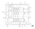
參閱圖3,要說明的是,當該電晶體開關T是使用P型薄膜電晶體時,該等發光二極體L也可以是共陽極結構,且組裝後的電連接方式為:位於同一列(column)排列的該等發光二極體L的負極與同一條相應的電源線232電連接並連接至該接地線路25,位於同一組裝子板30且同一行(row)排列的發光二極體L的正極與位於該組裝子板30的電晶體開關T的源極電連接,該電晶體開關T的閘極與相應的其中一條閘極線G電連接,汲極則電連接於一正電壓源(V)。由於其分時掃描控制方式與前述相同,故不再贅述。Referring to Figure 3, it should be noted that when the transistor switch T uses a P-type thin film transistor, the light-emitting diodes L can also have a common anode structure, and the electrical connection method after assembly is: located in the same column The negative electrodes of the light-emitting diodes L arranged in (column) are electrically connected to the same
於一些實施例中,用於組裝的每一組裝子板30的電晶體開關T的數量也可以是與該等發光二極體單元32的組數相對應。In some embodiments, the number of transistor switches T used for each
具體的說,參閱圖4,再以該電晶體開關T為N型電晶體為例說明。該每一組裝子板30具有多組發光二極體單元32,及多個數量與該等發光二極體單元32的組數相對應的電晶體開關T。每一個電晶體開關T的汲極分別對應電連接每一組發光二極體單元32的三個發光二極體L的負極,組裝後,位於同一個組裝子板30的兩個電晶體開關T的閘極則對應電連接於同一條閘極線G,其餘電連接關係如前所述,故不再多加說明。要說明的是,圖4是以該每一組發光二極體單元32對應電連接於同一個電晶體開關T為例,然實際實施時,也可以視需求及設計而以兩組、三組或多組發光二極體單元32電連接於同一個電晶體開關T,不以此為限。透過讓1個電晶體開關T帶載1組或多組發光二極體單元32,可減少寄生電容/電感效應提升顯示效果。Specifically, referring to Figure 4, the transistor switch T is an N-type transistor.Take an example to illustrate. Each
於另一些實施例中,於該組裝子板30的每一組發光二極體單元32的發光二極體L的數量也可以是3個以上。參閱圖5,圖5以該電晶體開關T為N型電晶體,且僅顯示該組裝子板30上的其中兩組發光二極體單元32,每組發光二極體單元32具有6個可發出不同光色(R、G、B)的發光二極體L,該等發光二極體L成兩排間隔交錯排列,再併接到該電晶體開關T,且所有的發光二極體L是電連接到同一個電晶體開關T為例說明。然而,實際實施時該發光二極體L的數量及排列方式並不以此為限,且該電晶體開關T的電晶體開關的數量也可以如前所述為一個電晶體開關T對應多組發光二極體單元32或每組發光二極體單元32均對應一個電晶體開關T。In other embodiments, the number of light-emitting diodes L in each group of light-emitting
要說明的是,該等發光二極體L的排列方式可以是如圖4所示以交錯方式間隔成行列方式排列,或是其它排列方式,只要是可讓組裝後的該等發光二極體L於該板體21的排列可符合顯示的需求設計且易於與相應的電源線232電連接即可,並無特別限制。It should be noted that the arrangement of the light-emitting diodes L can be arranged in rows and columns in a staggered manner as shown in Figure 4, or in other arrangements, as long as the light-emitting diodes L can be assembled The arrangement of the
綜上所述,本發明利用分段組裝方式,先將多組發光二極體單元32以分組轉移方式轉移至一面積較小的基板31,且每組發光二極體單元32具有多個發光二極體L,得到多個供用於組裝的組裝子板30。接著,再將多個已承載有多數發光二極體L的組裝子板30透過第二次組裝方式組設於該系統母板2的板體21。由於該組裝子板30的每一組發光二極體單元32是由多個發光二極體L組成,因此,在將該等發光二極體單元32轉移至該組裝子板30的基板31時可減少轉移次數而提高貼片效率。此外,當該等發光二極體L為微型發光二極體時,透過分段組裝方式將多片已承載有多組發光二極體單元32的組裝子板30組裝至該系統母板2的板體21,還可避免巨量轉移的對位公差問題及組裝過程該電路板的變形翹曲問題,而可更易於使用,故確實可達成本發明的目的。To sum up, the present invention uses a segmented assembly method to first transfer multiple groups of light-emitting
惟以上所述者,僅為本發明的實施例而已,當不能以此限定本發明實施的範圍,凡是依本發明申請專利範圍及專利說明書內容所作的簡單的等效變化與修飾,皆仍屬本發明專利涵蓋的範圍內。However, the above are only examples of the present invention and should not be used to limit the scope of the present invention. All simple equivalent changes and modifications made based on the patent scope of the present invention and the content of the patent specification are still within the scope of the present invention. Scope covered by the patent of this inventionwithin.
20:系統母板20:System motherboard
21:板體21:Plate body
22:時序控制單元22: Timing control unit
23:驅動電源電路單元23: Drive power circuit unit
231:驅動IC231:Driver IC
232:電源線232:Power cord
24:閘極控制電路單元24: Gate control circuit unit
241:閘極訊號控制器241: Gate signal controller
G:閘極線G: Gate line
25:接地線路25:Ground line
30:組裝子板30:Assemble the daughter board
L:發光二極體L: light emitting diode
Y:第一方向Y: first direction
X:第二方向X: second direction
Claims (10)
Translated fromChinesePriority Applications (3)
| Application Number | Priority Date | Filing Date | Title |
|---|---|---|---|
| TW111132112ATWI832395B (en) | 2022-08-25 | 2022-08-25 | Assembly type light emitting diode display device |
| CN202310981000.3ACN117636754A (en) | 2022-08-25 | 2023-08-07 | Assembled light-emitting diode display device |
| US18/446,498US12039924B2 (en) | 2022-08-25 | 2023-08-09 | Assembled light emitting diode display device |
Applications Claiming Priority (1)
| Application Number | Priority Date | Filing Date | Title |
|---|---|---|---|
| TW111132112ATWI832395B (en) | 2022-08-25 | 2022-08-25 | Assembly type light emitting diode display device |
Publications (2)
| Publication Number | Publication Date |
|---|---|
| TWI832395Btrue TWI832395B (en) | 2024-02-11 |
| TW202410440A TW202410440A (en) | 2024-03-01 |
Family
ID=89997087
Family Applications (1)
| Application Number | Title | Priority Date | Filing Date |
|---|---|---|---|
| TW111132112ATWI832395B (en) | 2022-08-25 | 2022-08-25 | Assembly type light emitting diode display device |
Country Status (3)
| Country | Link |
|---|---|
| US (1) | US12039924B2 (en) |
| CN (1) | CN117636754A (en) |
| TW (1) | TWI832395B (en) |
Families Citing this family (1)
| Publication number | Priority date | Publication date | Assignee | Title |
|---|---|---|---|---|
| TWI831343B (en)* | 2022-08-25 | 2024-02-01 | 聚積科技股份有限公司 | Light emitting diode display device |
Citations (3)
| Publication number | Priority date | Publication date | Assignee | Title |
|---|---|---|---|---|
| US20160343771A1 (en)* | 2014-09-25 | 2016-11-24 | X-Celeprint Limited | Small-aperture-ratio display with electrical component |
| CN113066427A (en)* | 2019-12-30 | 2021-07-02 | 乐金显示有限公司 | Pixel circuit, light-emitting display device and driving method thereof |
| TW202215636A (en)* | 2020-10-07 | 2022-04-16 | 聯嘉光電股份有限公司 | Grain structure of miniature light emitting diode display including a package carrier, at least one light emitting diode component, at least one metal-oxide-semiconductor field effect transistor (MOSFET) and a connecting line |
Family Cites Families (13)
| Publication number | Priority date | Publication date | Assignee | Title |
|---|---|---|---|---|
| KR20080016271A (en)* | 2006-08-18 | 2008-02-21 | 삼성전자주식회사 | OLED display and manufacturing method thereof |
| EP2104954B1 (en)* | 2007-01-17 | 2022-03-16 | The Board of Trustees of the University of Illinois | Optical systems fabricated by printing-based assembly |
| CN105789237A (en)* | 2016-04-25 | 2016-07-20 | 京东方科技集团股份有限公司 | LED display module, LED display device and manufacturing method of LED display module |
| CN114695425A (en)* | 2016-12-22 | 2022-07-01 | 夏普株式会社 | Display device and manufacturing method |
| FR3065116B1 (en)* | 2017-04-05 | 2021-08-27 | Commissariat Energie Atomique | LED TRANSMITTED IMAGE DISPLAY DEVICE |
| JP2019012767A (en)* | 2017-06-30 | 2019-01-24 | ルネサスエレクトロニクス株式会社 | Semiconductor module manufacturing method and semiconductor module |
| CN109309154B (en)* | 2018-10-12 | 2020-05-19 | 京东方科技集团股份有限公司 | Display unit, display substrate, preparation method of display substrate and display device |
| KR20190099149A (en)* | 2019-08-06 | 2019-08-26 | 엘지전자 주식회사 | Display device using micro-led |
| CN112714959B (en)* | 2019-08-27 | 2024-05-07 | 京东方科技集团股份有限公司 | Display substrate and manufacturing method thereof, and display device |
| CN111681598A (en)* | 2020-06-03 | 2020-09-18 | 深圳市华星光电半导体显示技术有限公司 | Display panel and manufacturing method thereof |
| JP2022000676A (en)* | 2020-06-19 | 2022-01-04 | 株式会社ジャパンディスプレイ | Method for manufacturing display device |
| CN117242559A (en)* | 2021-03-11 | 2023-12-15 | 应用材料公司 | Systems and methods for manufacturing micro LED displays |
| US12232399B2 (en)* | 2021-04-28 | 2025-02-18 | Boe Technology Group Co., Ltd. | Display substrate, display panel, and method of manufacturing display substrate having scan driving circuit in non-light-emitting region of pixel units |
- 2022
- 2022-08-25TWTW111132112Apatent/TWI832395B/enactive
- 2023
- 2023-08-07CNCN202310981000.3Apatent/CN117636754A/enactivePending
- 2023-08-09USUS18/446,498patent/US12039924B2/enactiveActive
Patent Citations (3)
| Publication number | Priority date | Publication date | Assignee | Title |
|---|---|---|---|---|
| US20160343771A1 (en)* | 2014-09-25 | 2016-11-24 | X-Celeprint Limited | Small-aperture-ratio display with electrical component |
| CN113066427A (en)* | 2019-12-30 | 2021-07-02 | 乐金显示有限公司 | Pixel circuit, light-emitting display device and driving method thereof |
| TW202215636A (en)* | 2020-10-07 | 2022-04-16 | 聯嘉光電股份有限公司 | Grain structure of miniature light emitting diode display including a package carrier, at least one light emitting diode component, at least one metal-oxide-semiconductor field effect transistor (MOSFET) and a connecting line |
Also Published As
| Publication number | Publication date |
|---|---|
| CN117636754A (en) | 2024-03-01 |
| US12039924B2 (en) | 2024-07-16 |
| US20240071298A1 (en) | 2024-02-29 |
| TW202410440A (en) | 2024-03-01 |
Similar Documents
| Publication | Publication Date | Title |
|---|---|---|
| US10847548B2 (en) | Led display device having TFT substrate provided with LED driver units | |
| CN108511485B (en) | display device | |
| TWI742705B (en) | Display apparatus | |
| CN113140589B (en) | Array substrate, display panel and display device | |
| TWI711199B (en) | Microled display panel | |
| CN112419908B (en) | Display device and semiconductor device | |
| US20230107672A1 (en) | Display panel and method for manufacturing same | |
| TWI672683B (en) | Display panel | |
| US20110157114A1 (en) | Electroluminescence device | |
| CN112673412B (en) | Display device | |
| CN112567522B (en) | Display device using semiconductor light emitting diode and method of manufacturing the same | |
| TWI832395B (en) | Assembly type light emitting diode display device | |
| CN110033709A (en) | Micro- LED display panel | |
| CN101764148A (en) | Electroluminescent device | |
| US12310192B2 (en) | Light-emission driving substrate, light-emitting panel, and display device | |
| TWI855489B (en) | Luminescent display device | |
| US12148364B2 (en) | Light emitting display device | |
| WO2022110015A1 (en) | Display substrate, display panel, and display device | |
| WO2022052058A1 (en) | Light emitting panel and preparation method therefor, and electronic device | |
| TWI831343B (en) | Light emitting diode display device | |
| TWI865259B (en) | Display panel and manufacturing method thereof | |
| US20240405001A1 (en) | Display device and method of manufacturing the same | |
| US20230275200A1 (en) | Display device using semiconductor light-emitting element, and method for manufacturing same | |
| TWI641108B (en) | Microled display panel | |
| CN114927511A (en) | Single-chip integrated large-area multicolor high-resolution display Micro-LED chip and manufacturing method thereof |