TWI829004B - Switching power supply system - Google Patents
Switching power supply systemDownload PDFInfo
- Publication number
- TWI829004B TWI829004BTW110129676ATW110129676ATWI829004BTW I829004 BTWI829004 BTW I829004BTW 110129676 ATW110129676 ATW 110129676ATW 110129676 ATW110129676 ATW 110129676ATW I829004 BTWI829004 BTW I829004B
- Authority
- TW
- Taiwan
- Prior art keywords
- field effect
- effect transistor
- mos field
- power mos
- voltage
- Prior art date
Links
- 230000005669field effectEffects0.000claimsabstractdescription307
- 230000000630rising effectEffects0.000claimsabstractdescription70
- 238000012512characterization methodMethods0.000claimsabstractdescription20
- 238000004804windingMethods0.000claimsabstractdescription9
- 239000003990capacitorSubstances0.000claimsdescription17
- 238000010586diagramMethods0.000description45
- 238000001514detection methodMethods0.000description15
- 238000000034methodMethods0.000description15
- 230000002159abnormal effectEffects0.000description9
- 230000008569processEffects0.000description7
- 239000004065semiconductorSubstances0.000description6
- 229910044991metal oxideInorganic materials0.000description5
- 150000004706metal oxidesChemical class0.000description5
- 239000013078crystalSubstances0.000description3
- 230000007423decreaseEffects0.000description3
- 238000012986modificationMethods0.000description3
- 230000004048modificationEffects0.000description3
- 230000000087stabilizing effectEffects0.000description3
- 230000008859changeEffects0.000description2
- 239000012634fragmentSubstances0.000description2
- 230000003071parasitic effectEffects0.000description2
- 230000005855radiationEffects0.000description2
- 238000006467substitution reactionMethods0.000description2
- 238000007792additionMethods0.000description1
- 230000005540biological transmissionEffects0.000description1
- 230000005347demagnetizationEffects0.000description1
- 230000000694effectsEffects0.000description1
- 230000005611electricityEffects0.000description1
- 238000005516engineering processMethods0.000description1
- 239000000835fiberSubstances0.000description1
- 230000006870functionEffects0.000description1
- 230000003287optical effectEffects0.000description1
Images


Classifications
- H—ELECTRICITY
- H02—GENERATION; CONVERSION OR DISTRIBUTION OF ELECTRIC POWER
- H02M—APPARATUS FOR CONVERSION BETWEEN AC AND AC, BETWEEN AC AND DC, OR BETWEEN DC AND DC, AND FOR USE WITH MAINS OR SIMILAR POWER SUPPLY SYSTEMS; CONVERSION OF DC OR AC INPUT POWER INTO SURGE OUTPUT POWER; CONTROL OR REGULATION THEREOF
- H02M3/00—Conversion of DC power input into DC power output
- H02M3/22—Conversion of DC power input into DC power output with intermediate conversion into AC
- H02M3/24—Conversion of DC power input into DC power output with intermediate conversion into AC by static converters
- H02M3/28—Conversion of DC power input into DC power output with intermediate conversion into AC by static converters using discharge tubes with control electrode or semiconductor devices with control electrode to produce the intermediate AC
- H02M3/325—Conversion of DC power input into DC power output with intermediate conversion into AC by static converters using discharge tubes with control electrode or semiconductor devices with control electrode to produce the intermediate AC using devices of a triode or a transistor type requiring continuous application of a control signal
- H02M3/335—Conversion of DC power input into DC power output with intermediate conversion into AC by static converters using discharge tubes with control electrode or semiconductor devices with control electrode to produce the intermediate AC using devices of a triode or a transistor type requiring continuous application of a control signal using semiconductor devices only
- H02M3/33569—Conversion of DC power input into DC power output with intermediate conversion into AC by static converters using discharge tubes with control electrode or semiconductor devices with control electrode to produce the intermediate AC using devices of a triode or a transistor type requiring continuous application of a control signal using semiconductor devices only having several active switching elements
- H—ELECTRICITY
- H02—GENERATION; CONVERSION OR DISTRIBUTION OF ELECTRIC POWER
- H02M—APPARATUS FOR CONVERSION BETWEEN AC AND AC, BETWEEN AC AND DC, OR BETWEEN DC AND DC, AND FOR USE WITH MAINS OR SIMILAR POWER SUPPLY SYSTEMS; CONVERSION OF DC OR AC INPUT POWER INTO SURGE OUTPUT POWER; CONTROL OR REGULATION THEREOF
- H02M3/00—Conversion of DC power input into DC power output
- H02M3/22—Conversion of DC power input into DC power output with intermediate conversion into AC
- H02M3/24—Conversion of DC power input into DC power output with intermediate conversion into AC by static converters
- H02M3/28—Conversion of DC power input into DC power output with intermediate conversion into AC by static converters using discharge tubes with control electrode or semiconductor devices with control electrode to produce the intermediate AC
- H02M3/325—Conversion of DC power input into DC power output with intermediate conversion into AC by static converters using discharge tubes with control electrode or semiconductor devices with control electrode to produce the intermediate AC using devices of a triode or a transistor type requiring continuous application of a control signal
- H02M3/335—Conversion of DC power input into DC power output with intermediate conversion into AC by static converters using discharge tubes with control electrode or semiconductor devices with control electrode to produce the intermediate AC using devices of a triode or a transistor type requiring continuous application of a control signal using semiconductor devices only
- H02M3/33507—Conversion of DC power input into DC power output with intermediate conversion into AC by static converters using discharge tubes with control electrode or semiconductor devices with control electrode to produce the intermediate AC using devices of a triode or a transistor type requiring continuous application of a control signal using semiconductor devices only with automatic control of the output voltage or current, e.g. flyback converters
- H02M3/33523—Conversion of DC power input into DC power output with intermediate conversion into AC by static converters using discharge tubes with control electrode or semiconductor devices with control electrode to produce the intermediate AC using devices of a triode or a transistor type requiring continuous application of a control signal using semiconductor devices only with automatic control of the output voltage or current, e.g. flyback converters with galvanic isolation between input and output of both the power stage and the feedback loop
- H—ELECTRICITY
- H02—GENERATION; CONVERSION OR DISTRIBUTION OF ELECTRIC POWER
- H02M—APPARATUS FOR CONVERSION BETWEEN AC AND AC, BETWEEN AC AND DC, OR BETWEEN DC AND DC, AND FOR USE WITH MAINS OR SIMILAR POWER SUPPLY SYSTEMS; CONVERSION OF DC OR AC INPUT POWER INTO SURGE OUTPUT POWER; CONTROL OR REGULATION THEREOF
- H02M1/00—Details of apparatus for conversion
- H02M1/08—Circuits specially adapted for the generation of control voltages for semiconductor devices incorporated in static converters
- H—ELECTRICITY
- H02—GENERATION; CONVERSION OR DISTRIBUTION OF ELECTRIC POWER
- H02M—APPARATUS FOR CONVERSION BETWEEN AC AND AC, BETWEEN AC AND DC, OR BETWEEN DC AND DC, AND FOR USE WITH MAINS OR SIMILAR POWER SUPPLY SYSTEMS; CONVERSION OF DC OR AC INPUT POWER INTO SURGE OUTPUT POWER; CONTROL OR REGULATION THEREOF
- H02M1/00—Details of apparatus for conversion
- H02M1/32—Means for protecting converters other than automatic disconnection
- H—ELECTRICITY
- H02—GENERATION; CONVERSION OR DISTRIBUTION OF ELECTRIC POWER
- H02M—APPARATUS FOR CONVERSION BETWEEN AC AND AC, BETWEEN AC AND DC, OR BETWEEN DC AND DC, AND FOR USE WITH MAINS OR SIMILAR POWER SUPPLY SYSTEMS; CONVERSION OF DC OR AC INPUT POWER INTO SURGE OUTPUT POWER; CONTROL OR REGULATION THEREOF
- H02M1/00—Details of apparatus for conversion
- H02M1/44—Circuits or arrangements for compensating for electromagnetic interference in converters or inverters
- H—ELECTRICITY
- H02—GENERATION; CONVERSION OR DISTRIBUTION OF ELECTRIC POWER
- H02M—APPARATUS FOR CONVERSION BETWEEN AC AND AC, BETWEEN AC AND DC, OR BETWEEN DC AND DC, AND FOR USE WITH MAINS OR SIMILAR POWER SUPPLY SYSTEMS; CONVERSION OF DC OR AC INPUT POWER INTO SURGE OUTPUT POWER; CONTROL OR REGULATION THEREOF
- H02M3/00—Conversion of DC power input into DC power output
- H02M3/22—Conversion of DC power input into DC power output with intermediate conversion into AC
- H02M3/24—Conversion of DC power input into DC power output with intermediate conversion into AC by static converters
- H02M3/28—Conversion of DC power input into DC power output with intermediate conversion into AC by static converters using discharge tubes with control electrode or semiconductor devices with control electrode to produce the intermediate AC
- H02M3/325—Conversion of DC power input into DC power output with intermediate conversion into AC by static converters using discharge tubes with control electrode or semiconductor devices with control electrode to produce the intermediate AC using devices of a triode or a transistor type requiring continuous application of a control signal
- H02M3/335—Conversion of DC power input into DC power output with intermediate conversion into AC by static converters using discharge tubes with control electrode or semiconductor devices with control electrode to produce the intermediate AC using devices of a triode or a transistor type requiring continuous application of a control signal using semiconductor devices only
- H02M3/33569—Conversion of DC power input into DC power output with intermediate conversion into AC by static converters using discharge tubes with control electrode or semiconductor devices with control electrode to produce the intermediate AC using devices of a triode or a transistor type requiring continuous application of a control signal using semiconductor devices only having several active switching elements
- H02M3/33576—Conversion of DC power input into DC power output with intermediate conversion into AC by static converters using discharge tubes with control electrode or semiconductor devices with control electrode to produce the intermediate AC using devices of a triode or a transistor type requiring continuous application of a control signal using semiconductor devices only having several active switching elements having at least one active switching element at the secondary side of an isolation transformer
- H02M3/33592—Conversion of DC power input into DC power output with intermediate conversion into AC by static converters using discharge tubes with control electrode or semiconductor devices with control electrode to produce the intermediate AC using devices of a triode or a transistor type requiring continuous application of a control signal using semiconductor devices only having several active switching elements having at least one active switching element at the secondary side of an isolation transformer having a synchronous rectifier circuit or a synchronous freewheeling circuit at the secondary side of an isolation transformer
Landscapes
- Engineering & Computer Science (AREA)
- Power Engineering (AREA)
- Physics & Mathematics (AREA)
- Electromagnetism (AREA)
- Dc-Dc Converters (AREA)
Abstract
Translated fromChineseDescription
Translated fromChinese本發明屬於積體電路領域,尤其涉及一種開關電源系統。The invention belongs to the field of integrated circuits, and in particular relates to a switching power supply system.
通常,在傳統的開關電源系統中,在連續導通模式(Continuous Conduction Mode,CCM)下,存在一次電力MOS場效電晶體導通沿和副邊電力MOS場效電晶體關斷沿交疊的情況,這會導致第一電力MOS場效電晶體和副邊電力MOS場效電晶體的電流過大,導致第二電力MOS場效電晶體在關斷沿產生很大的電壓Vds尖峰,並且第一電力MOS場效電晶體和第二電力MOS場效電晶體交疊導通的持續時間越長,第一電力MOS場效電晶體和第二電力MOS場效電晶體的電流過大,第二電力MOS場效電晶體在關斷沿的電壓Vds尖峰也越大。Usually, in a traditional switching power supply system, in the continuous conduction mode (CCM), there is a situation where the on-edge of the primary power MOS field effect transistor overlaps with the off-edge of the secondary power MOS field effect transistor. This will cause the current of the first power MOS field effect transistor and the secondary power MOS field effect transistor to be too large, causing the second power MOS field effect transistor to generate a large voltage Vds spike at the turn-off edge, and the first power MOS field effect transistor will The longer the overlapping conduction time of the power MOS field effect transistor and the second power MOS field effect transistor, the current of the first power MOS field effect transistor and the second power MOS field effect transistor is too large, and the second power MOS field effect transistor The voltage Vds peak at the turn-off edge is also larger.
本發明實施例提供一種開關電源系統,通過將PWM控制器配置為基於表徵系統的輸出電壓的輸出電壓表徵信號和第一電力MOS場效電晶體的導通時間,來控制PWM控制器中上管的閘極驅動電壓的上升速率,以至少部分地基於該上管的閘極驅動電壓的上升速率來控制系統的第一電力MOS場效電晶體的閘極驅動電壓的上升速率,從而降低第二電力MOS場效電晶體關斷後的VD尖峰幅度。Embodiments of the present invention provide a switching power supply system that controls the upper tube of the PWM controller by configuring the PWM controller to be based on an output voltage characterization signal that characterizes the output voltage of the system and the conduction time of the first power MOS field effect transistor. The rise rate of the gate drive voltage is to control the rise rate of the gate drive voltage of the first power MOS field effect transistor of the system based at least in part on the rise rate of the gate drive voltage of the high-side transistor, thereby reducing the second power VD peak amplitude after the MOS field effect transistor is turned off.
第一方面,本發明實施例提供一種開關電源系統,包括變壓器、與所述變壓器的一次繞組連接的第一電力MOS場效電晶體、以及控制所述第一電力MOS場效電晶體的導通與關斷的脈寬調變控制器,其中,所述脈寬調變控制器被配置為在所述開關電源系統處於預定狀態時:基於表徵所述開關電源系統的輸出電壓的輸出電壓表徵信號和所述第一電力MOS場效電晶體的導通時間,控制所述脈寬調變控制器中的第二電力MOS場效電晶體的閘極驅動電壓的上升速率;以及至少部分地基於所述第二電力MOS場效電晶體的閘極驅動電壓的上升速率,控制所述第一電力MOS場效電晶體的閘極驅動電壓的上升速率。In a first aspect, embodiments of the present invention provide a switching power supply system, including a transformer, a first power MOS field effect transistor connected to a primary winding of the transformer, and controlling the conduction and switching of the first power MOS field effect transistor. A turn-off pulse width modulation controller, wherein the pulse width modulation controller is configured to: when the switching power supply system is in a predetermined state: based on an output voltage characterization signal characterizing an output voltage of the switching power supply system and The first electricitythe conduction time of the force MOS field effect transistor, controlling the rise rate of the gate drive voltage of the second power MOS field effect transistor in the pulse width modulation controller; and based at least in part on the second power MOS field effect transistor The rising rate of the gate driving voltage of the field effect transistor controls the rising rate of the gate driving voltage of the first power MOS field effect transistor.
根據第一方面提供的開關電源系統,所述預定狀態包括以下項中的任一項:啟動狀態、輸出短路狀態和輸出超載狀態。According to the switching power supply system provided in the first aspect, the predetermined state includes any one of the following items: starting state, output short circuit state and output overload state.
根據第一方面提供的開關電源系統,所述脈寬調變控制器進一步被配置為:基於所述輸出電壓表徵信號和第一預設閾值的比較結果,以及上一週期的所述第一電力MOS場效電晶體的導通時間與第二預設閾值的比較結果,控制所述第二電力MOS場效電晶體的閘極驅動電壓的上升速率。According to the switching power supply system provided in the first aspect, the pulse width modulation controller is further configured to: based on a comparison result between the output voltage characterization signal and a first preset threshold, and the first power of the previous cycle The comparison result between the conduction time of the MOS field effect transistor and the second preset threshold controls the rising rate of the gate driving voltage of the second power MOS field effect transistor.
根據第一方面提供的開關電源系統,所述脈寬調變控制器進一步被配置為:通過控制連接在所述第二電力MOS場效電晶體的閘極和地之間的電容的充電速率,控制所述第二電力MOS場效電晶體的閘極驅動電壓的上升速率。According to the switching power supply system provided in the first aspect, the pulse width modulation controller is further configured to: by controlling the charging rate of the capacitor connected between the gate of the second power MOS field effect transistor and the ground, Control the rising rate of the gate driving voltage of the second power MOS field effect transistor.
根據第一方面提供的開關電源系統,所述脈寬調變控制器進一步被配置為:通過控制用於對所述電容提供充電電流的電流鏡的輸入電流的大小,控制所述第二電力MOS場效電晶體的閘極驅動電壓的上升速率。According to the switching power supply system provided in the first aspect, the pulse width modulation controller is further configured to: control the second power MOS by controlling the size of the input current of the current mirror used to provide charging current to the capacitor. The rate of rise of the gate drive voltage of the field effect transistor.
根據第一方面提供的開關電源系統,所述脈寬調變控制器進一步被配置為:在所述輸出電壓表徵信號高於所述第一預設閾值,並且上一週期的所述第一電力MOS場效電晶體的導通時間小於所述第二預設閾值的情況下,降低所述第二電力MOS場效電晶體的閘極驅動電壓的上升速率。According to the switching power supply system provided in the first aspect, the pulse width modulation controller is further configured to: when the output voltage representation signal is higher than the first preset threshold and the first power of the previous cycle When the conduction time of the MOS field effect transistor is less than the second preset threshold, the rising rate of the gate driving voltage of the second power MOS field effect transistor is reduced.
根據第一方面提供的開關電源系統,所述開關電源系統為返馳變換器系統。According to the switching power supply system provided in the first aspect, the switching power supply system is a flyback converter system.
第二方面,本發明實施例提供了一種開關電源系統,其特徵在於,包括變壓器、與所述變壓器的一次繞組連接的第三電力MOS場效電晶體、以及控制所述第三電力MOS場效電晶體的導通與關斷的脈寬調變控制器,其中,所述脈寬調變控制器被配置為在所述開關電源系統處於預定狀態時:基於表徵流經所述第三電力MOS場效電晶體的電流的電流表徵信號和所述開關電源系統的輸入電壓,控制所述脈寬調變控制器中的第四電力MOS場效電晶體的閘極驅動電壓的上升速率;以及至少部分地基於所述第四電力MOS場效電晶體的閘極驅動電壓的上升速率,控制所述第三電力MOS場效電晶體的閘極驅動電壓的上升速率。In a second aspect, embodiments of the present invention provide a switching power supply system, which is particularlyThe characteristic is that it includes a transformer, a third power MOS field effect transistor connected to the primary winding of the transformer, and a pulse width modulation controller that controls the turn-on and turn-off of the third power MOS field effect transistor, wherein , the pulse width modulation controller is configured to: when the switching power supply system is in a predetermined state: based on the current characterization signal characterizing the current flowing through the third power MOS field effect transistor and the switching power supply system. an input voltage that controls a rising rate of a gate drive voltage of a fourth power MOS field effect transistor in the pulse width modulation controller; and based at least in part on the gate drive of the fourth power MOS field effect transistor The rising rate of the voltage controls the rising rate of the gate driving voltage of the third power MOS field effect transistor.
根據第二方面提供的開關電源系統,所述預定狀態包括以下項中的任一項:啟動狀態、輸出短路狀態和輸出超載狀態。According to the switching power supply system provided in the second aspect, the predetermined state includes any one of the following items: starting state, output short circuit state and output overload state.
根據第二方面提供的開關電源系統,所述脈寬調變控制器進一步被配置為:基於所述電流表徵信號和第三預設閾值的比較結果,以及所述輸入電壓和第四預設閾值的比較結果,控制所述第四電力MOS場效電晶體的閘極驅動電壓的上升速率。According to the switching power supply system provided in the second aspect, the pulse width modulation controller is further configured to: based on a comparison result between the current characterization signal and a third preset threshold, and the input voltage and a fourth preset threshold. The comparison result controls the rising rate of the gate driving voltage of the fourth power MOS field effect transistor.
根據第二方面提供的開關電源系統,所述脈寬調變控制器進一步被配置為:通過控制連接在所述第四電力MOS場效電晶體的閘極和地之間的電容的充電速率,控制所述第四電力MOS場效電晶體的閘極驅動電壓的上升速率。According to the switching power supply system provided in the second aspect, the pulse width modulation controller is further configured to: by controlling the charging rate of the capacitor connected between the gate of the fourth power MOS field effect transistor and the ground, Control the rising rate of the gate driving voltage of the fourth power MOS field effect transistor.
根據第二方面提供的開關電源系統,所述脈寬調變控制器進一步被配置為:通過控制用於對所述電容提供充電電流的電流鏡的輸入電流的大小,控制所述第四電力MOS場效電晶體的閘極驅動電壓的上升速率。According to the switching power supply system provided in the second aspect, the pulse width modulation controller is further configured to: control the fourth power MOS by controlling the size of the input current of the current mirror used to provide charging current to the capacitor. The rate of rise of the gate drive voltage of the field effect transistor.
根據第二方面提供的開關電源系統,所述脈寬調變控制器進一步被配置為:在所述電流表徵信號高於所述第三預設閾值,並且所述輸入電壓高於所述第四預設閾值的情況下,降低所述第四電力MOS場效電晶體的閘極驅動電壓的上升速率。According to the switching power supply system provided in the second aspect, the pulse width modulation controller is further configured to: when the current representation signal is higher than the third preset threshold and the input voltage is higher than the fourth When the threshold is preset, the rising rate of the gate driving voltage of the fourth power MOS field effect transistor is reduced.
根據第二方面提供的開關電源系統,所述開關電源系統為返馳變換器系統。According to the switching power supply system provided in the second aspect, the switching power supply system isFlyback converter system.
本發明實施例的開關電源系統,能夠對第一電力MOS場效電晶體的閘極驅動電壓進行調整,以降低第二電力MOS場效電晶體關斷後的VD(Mosfet drain voltage)尖峰幅度。The switching power supply system of the embodiment of the present invention can adjust the gate driving voltage of the first power MOS field effect transistor to reduce the VD (Mosfet drain voltage) peak amplitude after the second power MOS field effect transistor is turned off.
100:開關電源系統100:Switching power supply system
110,210,310:PWM控制器110,210,310:PWM controller
1101:比較器1101: Comparator
S1:第一電力MOS場效電晶體S1: The first power MOS field effect transistor
S2:第二電力MOS場效電晶體S2: The second power MOS field effect transistor
Vds,VRsense,Vg:電壓Vds, VRsense, Vg: voltage
Vin:輸入電壓Vin: input voltage
Rsense:電阻Rsense: resistance
120:第二SR控制器120: Second SR controller
FB,CS GATE:引腳FB, CS GATE: pin
130:第二誤差放大器130: Second error amplifier
140:光耦140: Optocoupler
150:負載150:Load
t0,t1,t2,t3:時刻t0,t1,t2,t3: time
Lp:主電感Lp: main inductor
M1,M2,M3,M4,M5:MOS管M1, M2, M3, M4, M5: MOS tube
2101,1102,3102:高端驅動器2101,1102,3102: High-end driver
2102,1103,3103:低端驅動器2102,1103,3103: Low-end driver
1104,3104,2103:ocp比較器1104,3104,2103:ocp comparator
1105:Gate Ton檢測單元1105:Gate Ton detection unit
1106,3106:閘1106,3106:gate
Z1:穩壓二極體Z1: Zener diode
C1:電容C1: Capacitor
NMOS M1:驅動下管NMOS M1: driver lower tube
NMOS M2:驅動上管NMOS M2: driver upper tube
Vout:輸出電壓Vout: output voltage
Vth:的閾值電壓Vth: threshold voltage
Vfb:輸出電壓表徵信號Vfb: output voltage characterization signal
Vfb_th,Is1_th,Vin_th:預設閾值Vfb_th,Is1_th,Vin_th: preset threshold
Ton_th:預設時間閾值Ton_th: preset time threshold
3101:負載檢測單元3101: Load detection unit
M3,M4:電流鏡M3, M4: current mirror
3105:AC電壓檢測單元3105:AC voltage detection unit
為了更清楚地說明本發明實施例的技術方案,下面將對本發明實施例中所需要使用的附圖作簡單的介紹,對於本領域普通技術人員來講,在不付出創造性勞動的前提下,還可以根據這些附圖獲得其他的附圖。In order to explain the technical solutions of the embodiments of the present invention more clearly, the drawings required to be used in the embodiments of the present invention will be briefly introduced below. For those of ordinary skill in the art, without exerting creative efforts, they can also Additional drawings can be obtained from these drawings.
圖1示出了本發明一個實施例提供的開關電源系統100的架構示意圖;圖2示出了本發明實施例提供的開關電源系統在斷續導通模式(Discontinuous Conduction Mode,DCM)下各個信號的時序圖;圖3示出了本發明實施例提供的開關電源系統在CCM模式下各個信號的時序圖;圖4示出了現有技術提供的PWM控制器210的結構示意圖;圖5示出了本發明實施例提供的開關電源系統在輸出電壓快速下降時相應信號的時序圖;圖6示出了圖1提供的開關電源系統100中相應信號的時序圖;圖7示出了本發明實施例提供的開關電源系統在對第一電力MOS場效電晶體S1的閘極電壓進行調整前後對應的第一電力MOS場效電晶體S1的電壓Vds下降沿和第二電力MOS場效電晶體S2的閘極上的電壓下降沿的時序圖;圖8示出了本發明實施例提供的開關電源系統在對第一電力MOS場效電晶體S1的閘極電壓進行調整前後對應的第一電力MOS場效電晶體S1的電壓Vds下降沿、電阻Rsense上的電壓VRsense和第二電力MOS場效電晶體S2的汲極上的電壓的時序圖;圖9示出了圖1提供的開關電源系統100中的PWM控制器110的結構示意圖;以及圖10示出了本發明實施例提供的PWM控制器310的結構示意圖。Figure 1 shows a schematic architectural diagram of a switching
下面將詳細描述本發明的各個方面的特徵和示例性實施例,為了使本發明的目的、技術方案及優點更加清楚明白,以下結合附圖及具體實施例,對本發明進行進一步詳細描述。應理解,此處所描述的具體實施例僅被配置為解釋本發明,並不被配置為限定本發明。對於本領域技術人員來說,本發明可以在不需要這些具體細節中的一些細節的情況下實施。下面對實施例的描述僅僅是為了通過示出本發明的示例來提供對本發明更好的理解。Features and exemplary embodiments of various aspects of the present invention will be described in detail below. In order to make the purpose, technical solutions and advantages of the present invention clearer, the present invention will be described in further detail below with reference to the accompanying drawings and specific embodiments. It should be understood that the specific embodiments described herein are configured only to explain the invention and not to limit the invention. It will be apparent to one skilled in the art that the present invention may be practiced without some of these specific details. The following description of the embodiments is merely intended to provide a better understanding of the invention by illustrating examples of the invention.
需要說明的是,在本文中,諸如第一和第二等之類的關係術語僅僅用來將一個實體或者操作與另一個實體或操作區分開來,而不一定要求或者暗示這些實體或操作之間存在任何這種實際的關係或者順序。而且,術語“包括”、“包含”或者其任何其他變體意在涵蓋非排他性的包含,從而使得包括一系列要素的過程、方法、物品或者設備不僅包括那些要素,而且還包括沒有明確列出的其他要素,或者是還包括為這種過程、方法、物品或者設備所固有的要素。在沒有更多限制的情況下,由語句“包括……”限定的要素,並不排除在包括所述要素的過程、方法、物品或者設備中還存在另外的相同要素。It should be noted that in this article, relational terms such as first and second are only used to distinguish one entity or operation from another entity or operation, and do not necessarily require or imply that these entities or operations are mutually exclusive. any such actual relationship or sequence exists between them. Furthermore, the terms "comprises," "comprises," or any other variations thereof are intended to cover a non-exclusive inclusion such that a process, method, article, or apparatus that includes a list of elements includes not only those elements, but also those not expressly listed other elements, or elements inherent to the process, method, article or equipment. Without further limitation, an element defined by the statement "comprising..." does not exclude the presence of additional identical elements in a process, method, article, or device that includes the stated element.
為了解決現有技術問題,本發明實施例提供了一種開關電源系統。下面首先對本發明實施例所提供的開關電源系統進行介紹。In order to solve the existing technical problems, embodiments of the present invention provide a switching power supply system. The following first introduces the switching power supply system provided by the embodiment of the present invention.
圖1示出了本發明一個實施例提供的開關電源系統100的架構示意圖。如圖1所示,該開關電源系統100可以基於其輸入電壓和輸出電壓,將工作模式分為例如以下三種:臨界模式、斷續導通模式(Discontinuous Conduction Mode,DCM)和CCM模式。FIG. 1 shows a schematic architectural diagram of a switching
在圖1所示的實施例中,該開關電源系統100可以包括變壓器、與變壓器的一次繞組連接的電力MOS場效電晶體S1、電阻Rsense、用於控制電力MOS場效電晶體S1的導通與關斷的脈衝寬度調變(Pulse Width Modulation,PWM)控制器(也稱為脈寬調變控制器)110、與變壓器的二次繞組連接的電力MOS場效電晶體S2、用於控制電力MOS場效電晶體S2的導通與關斷的SR控制器120、第二誤差放大器130、第二光耦140以及電容C1和負載150等。In the embodiment shown in FIG. 1 , the switching
作為一個示例,PWM控制器110可以具有兩個輸入引腳(例如,FB和CS引腳)以及一個輸出引腳(例如,GATE引腳),其中FB引腳為第二誤差放大器130和光耦140的回饋信號輸入端,以接收用於表徵系統的輸出電壓Vout的輸出電壓表徵信號,CS引腳為電阻Rsense的電流信號輸入端,以接收流經電阻Rsense的電流信號,Gate引腳為電力MOS場效電晶體S1的閘極驅動輸出端,以控制電力MOS場效電晶體S1的導通與關斷。As an example, the
作為一個示例,系統的輸出端可以連接至誤差放大器130的輸入端,第二誤差放大器130的輸出端可以連接至光耦140的輸入端,光耦140的輸出端可以連接至PWM控制器110的FB引腳,PWM控制器130的CS引腳可以連接至電阻Rsense的遠離地的一端和電力MOS場效電晶體S1的源極,電力MOS場效電晶體S1的汲極可以連接至一次繞組,電力MOS場效電晶體S1的閘極可以連接至PWM控制器110的GATE引腳,並且SR控制器120的輸入端可以連接至電力MOS場效電晶體S2的汲極,電力MOS場效電晶體S2的閘極可以連接至SR控制器120的輸出端。As an example, the output terminal of the system can be connected to the input terminal of the
通過本發明實施例提供的開關電源系統100,通過利用PWM控制器110來接收表徵系統的輸出電壓的輸出電壓表徵信號,同時對電力MOS場效電晶體S1的導通時間進行檢測,以至少部分地基於該輸出電壓表徵信號和上一週期的電力MOS場效電晶體S1的導通時間來控制第一電力MOS場效電晶體S1的閘極驅動電壓的上升速率,這將在下面結合圖9進行詳細描述。Through the switching
應注意的是,該開關電源系統100僅僅是本發明實施例提供的開關電源系統的一種實現方式,在其他實施例中,可以採用開關電源系統的其他實現方式,例如本發明其他實施例還提供了一種用於基於流經第一電力MOS場效電晶體的電流的電流表徵信號和開關電源系統的輸入電壓(例如,AC電壓)來控制第一電力MOS場效電晶體的閘極驅動電壓的上升速率的開關電源系統,這將在下面進行介紹,這將在下面結合圖10進行詳細描述。It should be noted that the switching
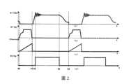
為了更好地理解本發明實施例提供的上述系統的工作原理,以下對系統的兩種工作模式進行詳細介紹:參考圖2,圖2示出了本發明實施例提供的開關電源系統在DCM模式下各個信號的時序圖。In order to better understand the working principle of the above system provided by the embodiment of the present invention, the two working modes of the system are introduced in detail below: Refer to Figure 2, which shows the switching power supply system provided by the embodiment of the present invention in DCM mode. Below are the timing diagrams of each signal.
如圖2所示,在DCM模式下,其中曲線(a)代表電力MOS場效電晶體S1的汲極與源極之間的電壓Vds與時間之間的關係的波形示意圖,曲線(b)代表電力MOS場效電晶體S1的閘極上的電壓與時間之間的關係的波形示意圖,曲線(c)代表電阻Rsense上的電壓與時間之間的關係的波形示意圖,以及曲線(d)代表電力MOS場效電晶體S2的閘極上的電壓與時間之間的關係的波形示意圖。As shown in Figure 2, in DCM mode, curve (a) represents the waveform diagram of the relationship between the voltage Vds between the drain and source of the power MOS field effect transistor S1 and time, and curve (b) represents The waveform diagram of the relationship between the voltage on the gate of the power MOS field effect transistor S1 and time, the curve (c) represents the waveform diagram of the relationship between the voltage on the resistor Rsense, and the curve (d) represents the power MOS A schematic waveform diagram of the relationship between the voltage on the gate of field effect transistor S2 and time.
作為一個示例,在時間段t0-t1期間,電力MOS場效電晶體S1處於導通狀態;在時刻t1,電力MOS場效電晶體S1關斷,電力MOS場效電晶體S1的電壓Vds開始上升;在時刻t2,第二SR控制器120檢測到滿足預設條件,接通電力MOS場效電晶體S2;在時刻t3,變壓器退磁結束,SR控制器120檢測到關斷信號後,可以斷開電力MOS場效電晶體S2,在時間段t2-t3期間,電力MOS場效電晶體S2處於導通狀態;在時間段t3-t4期間,主電感Lp和寄生電容諧振至最低電壓之後,使得電力MOS場效電晶體S1再次接通,進入下一週期。As an example, during the time period t0-t1, the power MOS field effect transistor S1 is in the on state; at time t1, the power MOS field effect transistor S1 is turned off, and the voltage Vds of the power MOS field effect transistor S1 begins to rise; At time t2, the
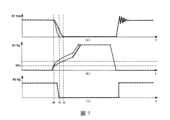
參考圖3,圖3示出了本發明實施例提供的開關電源系統在CCM模式下各個信號的時序圖。Referring to FIG. 3 , FIG. 3 shows a timing diagram of each signal of the switching power supply system provided by the embodiment of the present invention in the CCM mode.
如圖3所示,在CCM模式下,其中曲線(a)代表電力MOS場效電晶體S1的汲極與源極之間的電壓Vds與時間之間的關係的波形示意圖,曲線(b)代表電力MOS場效電晶體S1的閘極上的電壓與時間之間的關係的波形示意圖,曲線(c)代表電阻Rsense上的電壓與時間之間的關係的波形示意圖,以及曲線(d)代表電力MOS場效電晶體S2的閘極上的電壓與時間之間的關係的波形示意圖。As shown in Figure 3, in CCM mode, curve (a) represents the powerWaveform diagram of the relationship between the voltage Vds between the drain and source of the MOS field effect transistor S1 and time. Curve (b) represents the relationship between the voltage on the gate of the power MOS field effect transistor S1 and time. The waveform schematic diagram of Schematic diagram.
圖3的CCM模式與圖2的DCM模式之間的不同之處主要在於,在圖3中,在時刻t3,變壓器沒有完全退磁,電力MOS場效電晶體S1開始導通,電力MOS場效電晶體S1的電壓Vds快速下降,並且在時刻t3電力MOS場效電晶體S2處於導通狀態;在時刻t4,SR控制器120檢測到關斷信號後,可以快速斷開第二電力MOS場效電晶體S2,並且在時刻t4電力MOS場效電晶體S1處於導通狀態,可見,在時間段t3-t4期間,第一電力MOS場效電晶體S1和第二電力MOS場效電晶體S2同時導通,由於變壓器只有漏感參與第一電力MOS場效電晶體S1電流上升斜率很高,因此需要控制第一第二電力MOS場效電晶體同時導通的時間使其足夠短,本發明實施例提供的開關電源系統可以控制這個同時導通的時間,使其足夠短(例如,小於預設閾值),例如可以將第一第二電力MOS場效電晶體同時導通的時間控制在諸如20ns以內。The main difference between the CCM mode in Figure 3 and the DCM mode in Figure 2 is that in Figure 3, at time t3, the transformer is not completely demagnetized, the power MOS field effect transistor S1 begins to conduct, and the power MOS field effect transistor S1 begins to conduct. The voltage Vds of S1 drops rapidly, and the power MOS field effect transistor S2 is in the on state at time t3; after detecting the shutdown signal at time t4, the
此外,在一些實施例中,為了進一步降低第一第二電力MOS場效電晶體同時導通的時間,可以通過利用第二SR控制器120來快速關斷電力MOS場效電晶體S2,同時可以在第一第二電力MOS場效電晶體同時導通的時間期間,降低第一電力MOS場效電晶體S1導通時的電流,以降低電力MOS場效電晶體S1電壓Vds下降斜率等。In addition, in some embodiments, in order to further reduce the time for the first and second power MOS field effect transistors to be turned on at the same time, the
應注意,第一第二電力MOS場效電晶體同時導通的時間越長,會導致第一第二電力MOS場效電晶體的電流越大,這會導致電力MOS場效電晶體S2在關斷沿產生很大的電壓Vds尖峰。It should be noted that the longer the first and second power MOS field effect transistors are turned on at the same time, the greater the current of the first and second power MOS field effect transistors will be, which will cause the power MOS field effect transistor S2 to turn off at the turn-off edge. Produces a large voltage Vds spike.
因此,本發明實施例提供的開關電源系統,可以通過控制電力MOS場效電晶體S1的閘極輸出電壓在電力MOS場效電晶體開始導通時的電壓幅度(例如,Vgs),來降低電力MOS場效電晶體S1在第一第二電力MOS場效電晶體同時導通的時間期間的電流,這可以降低電力MOS場效電晶體S2在關斷沿的電壓Vds尖峰。Therefore, the switching power supply system provided by the embodiment of the present invention can control the gate output voltage of the power MOS field effect transistor S1 when the power MOS field effect transistor starts to conduct.The voltage amplitude (for example, Vgs) at the time is used to reduce the current of the power MOS field effect transistor S1 during the time when the first and second power MOS field effect transistors are turned on at the same time, which can reduce the power MOS field effect transistor S2 when the power MOS field effect transistor S2 is turned off. The voltage Vds spike at the off edge.
具體地,本發明實施例提供的開關電源系統,可以通過PWM控制器110來控制第一電力MOS場效電晶體S1的閘極驅動電壓的上升速率,來降低第二電力MOS場效電晶體S2在關斷沿的電壓Vds尖峰。Specifically, the switching power supply system provided by the embodiment of the present invention can use the
本發明實施例提供的PWM控制器可以具有多種實現方式,這將在下面進行介紹,為了更好地理解本發明實施例提供的PWM控制器,以下首先對現有技術提供的PWM控制器進行介紹。The PWM controller provided by the embodiment of the present invention can have multiple implementation methods, which will be introduced below. In order to better understand the PWM controller provided by the embodiment of the present invention, the PWM controller provided by the prior art is first introduced below.
如圖4所示,圖4示出了現有技術提供的PWM控制器210的結構示意圖。PWM控制器210包括由金屬氧化物半導體(Metal-Oxide-Semiconductor,MOS)電晶體M3和M4組成的電流鏡,MOS管M1、M2和M5,高端驅動器2101,低端驅動器2102,ocp比較器2103,穩壓二極體Z1,電容C1等。As shown in FIG. 4 , FIG. 4 shows a schematic structural diagram of a
其中,MOS管M5連接在電流鏡的輸出端與地之間,MOS管M5的閘極連接至高端驅動器2101的輸出端,高端驅動器2101的輸入端連接至ocp比較器的輸出端,ocp比較器的輸出端還連接至低端驅動器2102的輸入端,低端驅動器2102的輸出端連接至MOS管M1的閘極,MOS管M1和M2串聯連接在Vcc與地之間,MOS管M2的閘極連接至電流鏡的輸出端,ocp比較器的輸入端連接至電力MOS場效電晶體S1與電阻Rsense的公共端,MOS管M2的閘極還分別經由穩壓二極體Z1和電容C1接地。Among them, the MOS tube M5 is connected between the output terminal of the current mirror and the ground, the gate of the MOS tube M5 is connected to the output terminal of the high-
在傳統的PWM控制器中,當驅動下管(N型金屬氧化半導體,N type metal oxide semiconductor,NMOS)M1導通,且驅動上管NMOS M2斷開時,使得電力MOS場效電晶體S1的閘極處於低位準,此時電力MOS場效電晶體S1關斷。當驅動下管NMOS M1斷開,且驅動上管NMOS M2導通時,使得電力MOS場效電晶體S1的閘極處於高位準,此時電力MOS場效電晶體S1導通。驅動上管NMOS M2的源極連接至PWM控制器210的GATE引腳,驅動上管NMOS M2的閘極連接至P型金屬氧化半導體(P type metal oxide semiconductor,PMOS)M3和NMOS M5,組成PWM驅動器210的驅動級。其中,MOS管M2的閘極上的最高電壓由穩壓二極體Z1進行限制,以限制PWM控制器的GATE引腳處輸出的最高電壓。In the traditional PWM controller, when the driving lower tube (N-type metal oxide semiconductor, N-type metal oxide semiconductor, NMOS) M1 is turned on and the driving upper tube NMOS M2 is turned off, the gate of the power MOS field effect transistor S1 is turned off. The pole is at a low level, and the power MOS field effect transistor S1 is turned off at this time. When the driving lower transistor NMOS M1 is turned off and the driving upper transistor NMOS M2 is turned on, the gate of the power MOS field effect transistor S1 is at a high level. At this time, the power MOSField effect transistor S1 is turned on. The source of the upper driving transistor NMOS M2 is connected to the GATE pin of the
然而,在這種傳統的PWM控制器中,由於在CCM模式下,存在第一電力MOS場效電晶體和第二電力MOS場效電晶體同時導通的情況,這會導致第一電力MOS場效電晶體和第二電力MOS場效電晶體的電流過大,導致第二電力MOS場效電晶體在關斷沿產生很大的Vds尖峰,並且由於第一電力MOS場效電晶體和第二電力MOS場效電晶體同時導通的持續時間越長,導致第一電力MOS場效電晶體和第二電力MOS場效電晶體的電流越大,第二電力MOS場效電晶體在關斷沿的Vds尖峰也越大。However, in this traditional PWM controller, since in the CCM mode, there is a situation where the first power MOS field effect transistor and the second power MOS field effect transistor are turned on at the same time, this will cause the first power MOS field effect transistor to be turned on at the same time. The current of the crystal and the second power MOS field effect transistor is too large, causing the second power MOS field effect transistor to generate a large Vds spike at the turn-off edge, and due to the first power MOS field effect transistor and the second power MOS field effect transistor The longer the duration of the simultaneous conduction of the field effect transistors, the greater the current of the first power MOS field effect transistor and the second power MOS field effect transistor, and the higher the Vds peak of the second power MOS field effect transistor at the turn-off edge. The bigger.
可見,在現有技術的基礎上,本發明實施例提供的開關電源系統通過控制第一電力MOS場效電晶體的閘極驅動電壓的上升速率,可以防止第二電力MOS場效電晶體的Vds沖高。應注意,圖1提供的開關電源系統僅是本發明提供的開關電源系統的一種實現方式,其不旨在對本發明進行限制,且本發明實施例提供的開關電源系統還可以具有其他實現方式,這將在下面進行介紹。It can be seen that, based on the existing technology, the switching power supply system provided by the embodiment of the present invention can prevent the Vds surge of the second power MOS field effect transistor by controlling the rising rate of the gate driving voltage of the first power MOS field effect transistor. high. It should be noted that the switching power supply system provided in Figure 1 is only one implementation mode of the switching power supply system provided by the present invention. It is not intended to limit the present invention, and the switching power supply system provided by the embodiment of the present invention can also have other implementation modes. This will be covered below.
參考圖5,圖5示出了本發明實施例提供的開關電源系統在輸出電壓快速下降時相應信號的時序圖。Referring to FIG. 5 , FIG. 5 shows a timing diagram of corresponding signals when the output voltage of the switching power supply system provided by the embodiment of the present invention drops rapidly.
如圖5所示,在開關電源系統的輸出電壓Vout快速下降的情況下,系統工作模式由DCM模式進入深度CCM模式,其中曲線(a)代表開關電源系統的輸出電壓Vout與時間之間的關係的波形示意圖,曲線(b)代表第一電力MOS場效電晶體S1的汲極與源極之間的電壓Vds與時間之間的關係的波形示意圖,曲線(c)代表第一電力MOS場效電晶體S1的閘極上的電壓Vg與時間之間的關係的波形示意圖,以及曲線(d)代表第二電力MOS場效電晶體S2的閘極Vg上的電壓與時間之間的關係的波形示意圖。As shown in Figure 5, when the output voltage Vout of the switching power supply system drops rapidly, the system operating mode changes from DCM mode to deep CCM mode. Curve (a) represents the relationship between the output voltage Vout of the switching power supply system and time. The waveform schematic diagram of TransistorA schematic waveform diagram of the relationship between the voltage Vg on the gate electrode of S1 and time, and the curve (d) represents a schematic waveform diagram of the relationship between the voltage Vg on the gate electrode of the second power MOS field effect transistor S2 and time.
當系統工作在深度CCM模式下時,由於第二SR控制器120的工作模式差異,第一電力MOS場效電晶體和第二電力MOS場效電晶體在短時間內會有輕微共通,這會引起第二電力MOS場效電晶體S2電壓Vds沖高。When the system operates in the deep CCM mode, due to the difference in the working mode of the
為了解決上述問題,本發明實施例提供的開關電源系統通過降低第一電力MOS場效電晶體的閘極上的電壓的上升速率(如曲線(c)所示),減小第一電力MOS場效電晶體和第二電力MOS場效電晶體共通電流的幅度,以減小第二電力MOS場效電晶體S2的電壓Vds尖峰。In order to solve the above problem, the switching power supply system provided by the embodiment of the present invention reduces the first power MOS field effect transistor by reducing the rising rate of the voltage on the gate of the first power MOS field effect transistor (as shown in curve (c)). The amplitude of the common current between the transistor and the second power MOS field effect transistor is to reduce the voltage Vds spike of the second power MOS field effect transistor S2.
下面結合圖6的時序圖對圖1提供的開關電源系統100的工作原理進行介紹,參見圖6,圖6示出了圖1提供的開關電源系統100中相應信號的時序圖。The working principle of the switching
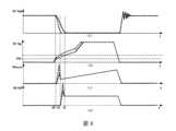
如圖6所示,在開關電源系統的輸出電壓Vout快速下降的情況下,系統工作模式由DCM模式進入深度CCM模式,其中曲線(a)代表開關電源系統的輸出電壓Vout與時間之間的關係的波形示意圖,曲線(b)代表PWM控制器110的引腳FB上的電壓與時間之間的關係的波形示意圖,曲線(c)代表第一電力MOS場效電晶體S1的閘極上的電壓Vg與時間之間的關係的波形示意圖,以及曲線(d)代表副邊電力MOS場效電晶體S2的閘極Vg上的電壓與時間之間的關係的波形示意圖。As shown in Figure 6, when the output voltage Vout of the switching power supply system drops rapidly, the system operating mode changes from DCM mode to deep CCM mode. Curve (a) represents the relationship between the output voltage Vout of the switching power supply system and time. The waveform schematic diagram of The waveform schematic diagram of the relationship between the voltage and time, and the curve (d) represents the waveform schematic diagram of the relationship between the voltage on the gate Vg of the secondary power MOS field effect transistor S2 and time.
作為一個示例,當輸出電壓Vout快速下降時,PWM控制器110的引腳FB上的電壓由正常工作電壓快速上升開環,其中,引腳FB接收第二誤差放大器光耦回饋信號,本發明實施例提供的PWM控制器通過基於例如表徵輸出電壓的輸出電壓表徵信號(例如,信號FB)和電力MOS場效電晶體S1的導通時間(圖中未示出)來控制第一電力MOS場效電晶體S1的閘極驅動電壓的上升速率。As an example, when the output voltage Vout drops rapidly, the voltage on the pin FB of the
具體地,參見圖6中的曲線(b),在時刻t1,輸出電壓表徵信號FB開始超過預設閾值(例如,Vfb_th),並且上一週期的電力MOS場效電晶體S1的導通時間開始小於預設閾值(例如,Ton_th),此時PWM控制器110開始降低第一電力MOS場效電晶體S1的閘極上的電壓的上升速率(參見曲線(c)),以降低電力MOS場效電晶體S2在關斷沿的Vds尖峰。Specifically, referring to curve (b) in Figure 6, at time t1, the output voltage representation signal FB begins to exceed the preset threshold (for example, Vfb_th), and the conduction time of the power MOS field effect transistor S1 in the previous cycle begins to be less than The threshold is preset (for example, Ton_th). At this time, the
作為一個示例,參考圖7,圖7示出了本發明實施例提供的開關電源系統在對第一電力MOS場效電晶體S1的閘極電壓進行調整前後對應的第一電力MOS場效電晶體S1的Vds下降沿和第二電力MOS場效電晶體S2的閘極上的電壓下降沿的時序圖。As an example, refer to FIG. 7 , which shows the corresponding first power MOS field effect transistor before and after adjusting the gate voltage of the first power MOS field effect transistor S1 in the switching power supply system provided by the embodiment of the present invention. Timing diagram of the falling edge of Vds of S1 and the falling edge of the voltage on the gate of the second power MOS field effect transistor S2.
如圖7所示,其中曲線(a)代表電力MOS場效電晶體S1的電壓Vds與時間之間的關係的波形示意圖,曲線(b)代表電力MOS場效電晶體S1的閘極電壓Vg與時間之間的關係的波形示意圖,以及曲線(c)代表電力MOS場效電晶體S2的閘極電壓Vg與時間之間的關係的波形示意圖。As shown in Figure 7, curve (a) represents the waveform diagram of the relationship between the voltage Vds of the power MOS field effect transistor S1 and time, and the curve (b) represents the gate voltage Vg of the power MOS field effect transistor S1 and The waveform schematic diagram of the relationship between time, and the curve (c) represents the waveform schematic diagram of the relationship between the gate voltage Vg of the power MOS field effect transistor S2 and time.
在時刻t0,第一電力MOS場效電晶體S1的閘極電壓上升至電力MOS場效電晶體S1的閾值電壓Vth,此時電力MOS場效電晶體S1開始導通,在未對電力MOS場效電晶體S1的閘極電壓進行調整之前,電力MOS場效電晶體S1的閘極電壓的上升速率較快(對應於曲線(b)中的虛線),此時電力MOS場效電晶體S1的電壓Vds的下降速率也較快(對應於曲線(a)中的虛線);在對電力MOS場效電晶體S1的閘極電壓進行調整之後,電力MOS場效電晶體S1的閘極電壓的上升速率較慢(對應於曲線(b)中的實線),此時電力MOS場效電晶體S1的電壓Vds的下降速率也較慢(對應於曲線(a)中的實線)。At time t0, the gate voltage of the first power MOS field effect transistor S1 rises to the threshold voltage Vth of the power MOS field effect transistor S1. At this time, the power MOS field effect transistor S1 begins to conduct. Before the gate voltage of transistor S1 is adjusted, the gate voltage of power MOS field effect transistor S1 rises faster (corresponding to the dotted line in curve (b)). At this time, the voltage of power MOS field effect transistor S1 The falling rate of Vds is also faster (corresponding to the dashed line in curve (a)); after adjusting the gate voltage of the power MOS field effect transistor S1, the rising rate of the gate voltage of the power MOS field effect transistor S1 Slower (corresponding to the solid line in curve (b)), at this time, the voltage Vds of the power MOS field effect transistor S1 decreases at a slower rate (corresponding to the solid line in curve (a)).
應注意的是,在對電力MOS場效電晶體S1的閘極電壓進行調整前後對應的電力MOS場效電晶體S2的閘極電壓在曲線(c)中示出為一條實線,並不旨在表示在對電力MOS場效電晶體S1的閘極電壓進行調整前後對應的電力MOS場效電晶體S2的閘極電壓未發生變化,實際上,電力MOS場效電晶體S2的閘極電壓發生細微變化,為了簡化描述,圖7中的曲線(c)中未示出。It should be noted that the gate voltage of the corresponding power MOS field effect transistor S2 before and after the adjustment of the gate voltage of the power MOS field effect transistor S1 is shown as a solid line in curve (c), which does not mean that the corresponding gate voltage of the power MOS field effect transistor S2 is adjusted. It means that the gate voltage of the corresponding power MOS field effect transistor S2 does not change before and after the adjustment of the gate voltage of the power MOS field effect transistor S1. In fact, the gate voltage of the power MOS field effect transistor S2 changes. Subtle changes are not shown in curve (c) in Figure 7 in order to simplify the description.
作為一個示例,第二SR控制器120需要在檢測到漏端信號之後再關斷電力MOS場效電晶體S2,由於SR控制器內部的檢測延時和驅動的關斷延時基本固定,所以在時間段t0-t1期間,SR控制器的關斷延時時間基本不變。As an example, the
從圖7中可以看出,當電力MOS場效電晶體S1的閘極電壓以較快斜率上升時,電力MOS場效電晶體S1的開關損耗集中在t0-t1時間段內,每次導通的損耗相對較小;當電力MOS場效電晶體S1的閘極電壓以較慢斜率上升時,電力MOS場效電晶體S1的開關損耗集中在t0-t2時間段內,每次導通的損耗相對較大。It can be seen from Figure 7 that when the gate voltage of the power MOS field effect transistor S1 rises at a faster slope, the switching loss of the power MOS field effect transistor S1 is concentrated in the t0-t1 time period, and each turn-on The loss is relatively small; when the gate voltage of the power MOS field effect transistor S1 rises at a slower slope, the switching loss of the power MOS field effect transistor S1 is concentrated in the t0-t2 time period, and the loss of each conduction is relatively small. big.
綜上,本發明實施例提供的開關電源系統在正常工作模式下,可以適當升高電力MOS場效電晶體S1的閘極電壓的上升速率,因為更快的上升速率可以得到更高的系統效率;本發明實施例提供的開關電源系統在異常工作模式下(例如,輸出電壓快速下降(輸出短路)和啟動狀態),可以適當降低電力MOS場效電晶體S1的閘極電壓的上升斜率,以避免第二電力MOS場效電晶體S2過高的Vds尖峰。In summary, the switching power supply system provided by the embodiment of the present invention can appropriately increase the rising rate of the gate voltage of the power MOS field effect transistor S1 in the normal operating mode, because a faster rising rate can achieve higher system efficiency. ; The switching power supply system provided by the embodiment of the present invention can appropriately reduce the rising slope of the gate voltage of the power MOS field effect transistor S1 in abnormal operating modes (for example, a rapid drop in output voltage (output short circuit) and startup state), so as to Avoid excessively high Vds spikes on the second power MOS field effect transistor S2.
作為一個示例,參考圖8,圖8示出了本發明實施例提供的開關電源系統在對第一電力MOS場效電晶體S1的閘極電壓進行調整前後對應的第一電力MOS場效電晶體S1的Vds下降沿、電阻Rsense上的電壓VRsense和第二電力MOS場效電晶體S2的汲極上的電壓的時序圖。As an example, refer to FIG. 8 , which shows the corresponding first power MOS field effect transistor before and after adjusting the gate voltage of the first power MOS field effect transistor S1 in the switching power supply system provided by the embodiment of the present invention. Timing diagram of the falling edge of Vds of S1, the voltage VRsense on the resistor Rsense and the voltage on the drain of the second power MOS field effect transistor S2.
如圖8所示,其中曲線(a)代表電力MOS場效電晶體S1的電壓Vds與時間之間的關係的波形示意圖,曲線(b)代表電力MOS場效電晶體S1的閘極電壓Vg與時間之間的關係的波形示意圖,曲線(c)代表電阻Rsense上的電壓VRsense與時間之間的關係的波形示意圖以及第二電力MOS場效電晶體S2的汲極上的電壓與時間之間的關係的波形示意圖。As shown in Figure 8, curve (a) represents the waveform diagram of the relationship between the voltage Vds of the power MOS field effect transistor S1 and time, and curve (b) represents the power MOS fieldA schematic waveform diagram of the relationship between the gate voltage Vg of the field effect transistor S1 and time. Curve (c) represents a waveform diagram of the relationship between the voltage VRsense on the resistor Rsense and time and the waveform diagram of the second power MOS field effect transistor S2. Waveform diagram of the relationship between voltage on the drain and time.
在時刻t0,第一電力MOS場效電晶體S1的閘極電壓上升至電力MOS場效電晶體S1的閾值電壓Vth,此時電力MOS場效電晶體S1開始導通,在未對電力MOS場效電晶體S1的閘極電壓進行調整之前,電力MOS場效電晶體S1的閘極電壓的上升速率較快(對應於曲線(b)中的虛線),此時電力MOS場效電晶體S1的電壓Vds的下降速率也較快(對應於曲線(a)中的虛線),電阻Rsense上的電壓VRsense較大(對應於曲線(c)中的虛線),且電力MOS場效電晶體S2的汲極上的電壓(即,尖峰)也較高(對應於曲線(d)中的虛線);在對電力MOS場效電晶體S1的閘極電壓進行調整之後,電力MOS場效電晶體S1的閘極電壓的上升速率較慢(對應於曲線(b)中的實線),此時電力MOS場效電晶體S1的電壓Vds的下降速率也較慢(對應於曲線(a)中的實線),電阻Rsense上的電壓VRsense較小(對應於曲線(c)中的實線),且第二電力MOS場效電晶體S2的汲極上的電壓也較小(對應於曲線(d)中的實線)。At time t0, the gate voltage of the first power MOS field effect transistor S1 rises to the threshold voltage Vth of the power MOS field effect transistor S1. At this time, the power MOS field effect transistor S1 begins to conduct. Before the gate voltage of transistor S1 is adjusted, the gate voltage of power MOS field effect transistor S1 rises faster (corresponding to the dotted line in curve (b)). At this time, the voltage of power MOS field effect transistor S1 The decrease rate of Vds is also faster (corresponding to the dotted line in curve (a)), the voltage VRsense on the resistor Rsense is larger (corresponding to the dotted line in curve (c)), and the drain electrode of the power MOS field effect transistor S2 The voltage (i.e., spike) is also higher (corresponding to the dashed line in curve (d)); after adjusting the gate voltage of the power MOS field effect transistor S1, the gate voltage of the power MOS field effect transistor S1 The rise rate is slower (corresponding to the solid line in curve (b)). At this time, the voltage Vds of the power MOS field effect transistor S1 also falls slowly (corresponding to the solid line in curve (a)). The resistance The voltage VRsense on Rsense is smaller (corresponding to the solid line in curve (c)), and the voltage on the drain electrode of the second power MOS field effect transistor S2 is also small (corresponding to the solid line in curve (d)) .
可見,不同的第一電力MOS場效電晶體的閘極電壓上升速率,對應于不同的第一電阻Rsense上的電壓波形以及副邊電力MOS場效電晶體的汲極電壓的尖峰波形。當第一電力MOS場效電晶體S1的閘極電壓上升,此時副邊電力MOS場效電晶體S2處於導通狀態,電力MOS場效電晶體S1的閘極電壓的上升斜率越大,即電力MOS場效電晶體S1的導通電流的上升斜率越高(變壓器的副邊處於短路狀態,漏感遠小於主電感),在電力MOS場效電晶體S2關斷後變壓器副邊對VD端寄生電容充電引起的正向尖峰也越高。It can be seen that different gate voltage rise rates of the first power MOS field effect transistor correspond to different voltage waveforms on the first resistor Rsense and peak waveforms of the drain voltage of the secondary power MOS field effect transistor. When the gate voltage of the first power MOS field effect transistor S1 rises, the secondary power MOS field effect transistor S2 is in the conductive state. The greater the rising slope of the gate voltage of the power MOS field effect transistor S1, that is, the power The higher the rising slope of the on-current of the MOS field effect transistor S1 (the secondary side of the transformer is in a short-circuit state, and the leakage inductance is much smaller than the main inductance), the parasitic capacitance of the secondary side of the transformer to the VD end after the power MOS field effect transistor S2 is turned off The positive spike caused by charging is also higher.
其中,汲極電流可以表示為公式(1),且第一電阻Rsense上的電壓VRsense可以表示為公式(2):Id=K*(VGS-Vth)2 (1)Among them, the drain current can be expressed as formula (1), and the voltage VRsense on the first resistor Rsense can be expressed as formula (2): Id=K*(VGS-Vth)2 (1)
VRsense=Id * Rsense (2)VRsense=Id * Rsense (2)
綜上,可見,為了優化電磁干擾(Electromagnetic Interference,EMI)輻射,本發明實施例提供的開關電源系統需要對電力MOS場效電晶體S1的閘極電壓的上升速率進行調整,也就是說,需要對PWM控制器的GATE引腳上的電壓上升沿進行調整,即需要對PWM控制器中的電力MOS場效電晶體M2(參見圖4)的源極電壓進行調整,由於電力MOS場效電晶體M2的源極電壓跟隨其閘極電壓,所以需要對電力MOS場效電晶體M2的閘極電壓(Net Vg)的上升速率進行調整,為了調整電力MOS場效電晶體M2的閘極電壓的上升速率,可以通過對M4/M3電流幅度和Vg對地電容C1進行調整的方式實現。In summary, it can be seen that in order to optimize electromagnetic interference (EMI) radiation, the switching power supply system provided by the embodiment of the present invention needs to adjust the rising rate of the gate voltage of the power MOS field effect transistor S1. That is to say, it needs to To adjust the rising edge of the voltage on the GATE pin of the PWM controller, it is necessary to adjust the source voltage of the power MOS field effect transistor M2 (see Figure 4) in the PWM controller. Since the power MOS field effect transistor The source voltage of M2 follows its gate voltage, so the rise rate of the gate voltage (Net Vg) of the power MOS field effect transistor M2 needs to be adjusted. In order to adjust the rise of the gate voltage of the power MOS field effect transistor M2 The speed can be achieved by adjusting the M4/M3 current amplitude and Vg to ground capacitance C1.
通常,可以將電力MOS場效電晶體S1的閘極電壓上升沿設計為三段式,其中,第一段,電力MOS場效電晶體S1的閘極電壓低於電力MOS場效電晶體S1的閾值電壓Vth,此時電力MOS場效電晶體S1處於關斷狀態,電壓Vg(參見圖4)快速上升;第二段,電力MOS場效電晶體鏡像(Mirror)平臺,減小前級的驅動電流以減慢電壓Vg的上升斜率,以減小EMI輻射干擾;以及第三段,電力MOS場效電晶體S1已經完全導通,增大前級的驅動電流以加快電壓Vg的上升斜率,使得電力MOS場效電晶體S1的閘極電壓可以快速上升,以此方式,可以減少電力MOS場效電晶體S1的開關損耗並提高系統的效率。Generally, the rising edge of the gate voltage of the power MOS field effect transistor S1 can be designed as a three-stage type. In the first stage, the gate voltage of the power MOS field effect transistor S1 is lower than that of the power MOS field effect transistor S1. Threshold voltage Vth, at this time the power MOS field effect transistor S1 is in the off state, and the voltage Vg (see Figure 4) rises rapidly; in the second section, the power MOS field effect transistor mirror (Mirror) platform reduces the drive of the front stage The current slows down the rising slope of voltage Vg to reduce EMI radiation interference; and in the third section, the power MOS field effect transistor S1 has been fully turned on, increasing the driving current of the front stage to speed up the rising slope of voltage Vg, so that the power The gate voltage of the MOS field effect transistor S1 can rise rapidly. In this way, the switching loss of the power MOS field effect transistor S1 can be reduced and the efficiency of the system can be improved.
本發明實施例提供的PWM控制器主要通過在異常情況下,減慢電力MOS場效電晶體S1的閘極電壓的上升速率,來避免副邊電力MOS場效電晶體S2過高的電壓Vds尖峰。The PWM controller provided by the embodiment of the present invention mainly avoids excessive voltage Vds spikes of the secondary power MOS field effect transistor S2 by slowing down the rising rate of the gate voltage of the power MOS field effect transistor S1 under abnormal conditions. .
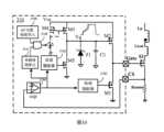
以下對本發明實施例提供的PWM控制器的第一種具體實現方式進行詳細介紹。參考圖9,圖9示出了圖1提供的開關電源系統100中的PWM控制器110的結構示意圖。The first specific implementation manner of the PWM controller provided by the embodiment of the present invention is introduced in detail below. Referring to FIG. 9 , FIG. 9 shows a schematic structural diagram of the
如圖9所示,用於控制電力MOS場效電晶體S1的導通與關斷的PWM控制器110可以包括FB引腳、Gate引腳和CS引腳。其中,PWM控制器110中的元件可以包括與FB引腳連接的比較器1101、由M3和M4組成的電流鏡,電力MOS場效電晶體M1、M2和M5,高端驅動器1102,低端驅動器1103,ocp比較器1104,Gate Ton檢測單元1105(可以用於例如對PWM控制器110的Gate引腳處的Ton時間進行檢測,換句話說,可以用於檢測電力MOS場效電晶體S1的導通時間),及閘1106,穩壓二極體Z1以及電容C1。As shown in FIG. 9 , the
作為一個示例,圖9提供的PWM控制器110可以基於例如表徵開關電源系統100的輸出電壓的輸出電壓表徵信號(例如,Vfb)以及上一週期的電力MOS場效電晶體S1的導通時間,控制PWM控制器110中的電力MOS場效電晶體M2的閘極驅動電壓的上升速率,以至少部分地基於電力MOS場效電晶體M2的閘極驅動電壓的上升速率來控制第一電力MOS場效電晶體S1的閘極驅動電壓的上升速率。As an example, the
具體地,結合圖1和圖9,在開關電源系統100處於異常狀態時,比較器1101可以接收經誤差放大器130和光耦140處理的輸出電壓,將表徵該輸出電壓的輸出電壓表徵信號Vfb(即,經處理的輸出電壓)與預設閾值Vfb_th進行比較,得到第一比較結果,並且可以利用例如Gate Ton檢測單元1105對上一週期的電力MOS場效電晶體S1的導通時間與預設閾值(例如,Ton_th)進行比較,得到第二比較結果,以將第一比較結果和第二比較結果輸出至及閘1106的兩個輸入端,使得及閘1106可以基於第一比較結果和第二比較結果來控制電流鏡的輸入偏置電流,例如,當輸出電壓表徵信號Vfb上升達到預設閾值Vfb_th,並且上一週期的電力MOS場效電晶體S1的導通時間下降達到預設時間閾值Ton_th之後,可以通過利用及閘1106來降低該輸入偏置電流,其中,Vfb_th為系統處於非正常負載情況(例如,啟動狀態和輸出短路的情況)下的預設電壓,通過降低輸入偏置電流可以降低電流鏡的輸出電流,降低該輸出電流可以降低電力MOS場效電晶體M2的閘極對地電容C1上的充電電流,通過降低電容C1上的充電電流可以降低電力MOS場效電晶體M2的閘極電壓的上升速率,通過降低電力MOS場效電晶體M2的閘極電壓的上升速率可以降低電力MOS場效電晶體M2的源極電壓的上升速率,通過降低電力MOS場效電晶體M2的源極電壓的上升速率可以降低PWM控制器110的Gate引腳上的電壓,進而降低電力MOS場效電晶體S1的閘極電壓的上升斜率,實現減慢電力MOS場效電晶體S1的閘極的第二段驅動。Specifically, with reference to FIGS. 1 and 9 , when the switching
應注意,在相同負載下,開關電源系統的輸入電壓Vin越高,電力MOS場效電晶體S1的大導通時間越短。在滿足輸出電壓表徵信號FB大於預設閾值的情況下,如果檢測PWM控制器的Gate引腳處輸出的位準處於高位準的時間小於預設閾值Ton_th,則可以判斷輸入電壓Vin為高壓輸入。作為一個示例,系統上高壓輸入和重載條件下副邊電力MOS場效電晶體S2關斷後的Vds尖峰幅度最大,本發明實施例提供的PWM控制器可以在同時滿足FB電壓和電力MOS場效電晶體S1的導通時間的條件下,實現減慢電力MOS場效電晶體S1的第二段驅動,這可以降低第二SR電力MOS場效電晶體S2關斷後的電壓Vds尖峰幅度。It should be noted that under the same load, the higher the input voltage Vin of the switching power supply system, the shorter the maximum conduction time of the power MOS field effect transistor S1. Under the condition that the output voltage characterization signal FB is greater than the preset threshold, if the time when the output level at the Gate pin of the PWM controller is detected to be at a high level is less than the preset threshold Ton_th, it can be determined that the input voltage Vin is a high-voltage input. As an example, under high-voltage input and heavy load conditions on the system, the Vds spike amplitude is the largest after the secondary power MOS field effect transistor S2 is turned off. The PWM controller provided by the embodiment of the present invention can satisfy the FB voltage and power MOS field at the same time. Under the condition of the conduction time of the power MOS field effect transistor S1, the second stage driving of the power MOS field effect transistor S1 is slowed down, which can reduce the voltage Vds peak amplitude after the second SR power MOS field effect transistor S2 is turned off.
可見,本發明實施例提供的PWM控制器110可以通過在表徵信號Vfb上升達到閾值Vfb_th,並且上一週期的電力MOS場效電晶體S1的導通時間下降達到閾值Ton_th之後,減慢電力MOS場效電晶體S1的閘極的第二段驅動,來在電力MOS場效電晶體S1開始導通時限制電力MOS場效電晶體S1的電流,減小電力MOS場效電晶體S1 Vds下降的斜率,以降低副邊電力MOS場效電晶體S2關斷後的電壓Vds尖峰。It can be seen that the
在一些實施例中,異常狀態可以包括以下項中的任一項:啟動狀態、輸出短路狀態和輸出超載狀態。In some embodiments, the abnormal state may include any of the following: a startup state, an output short circuit state, and an output overload state.
其中,輸出短路狀態是指系統因為外界原因造成輸出埠的正負兩端直接或近似短接在一起;在輸出短路狀態下,第一電力MOS場效電晶體S1的電流會達到最大值,由於輸出電壓很低變壓器不能退磁,系統工作在深度CCM模式,系統功耗會比較大,長時間工作的話甚至可能導致系統被損壞。輸出超載狀態是指系統的負載太大,超出帶載能力以至於系統不能正常工作;在輸出超載狀態下,第一晶片會以最大電流、或者功率的方式工作,為副邊輸出能量,此時如果不做特殊處理則系統功耗會比較大甚至導致系統被損壞。Among them, the output short-circuit state means that the positive and negative ends of the output port of the system are directly or approximately short-circuited together due to external reasons; in the output short-circuit state, the current of the first power MOS field effect transistor S1 will reach the maximum value. Due to the output If the voltage is very low, the transformer cannot be demagnetized, and the system works in deep CCM mode, which consumes a lot of power. If it works for a long time, the system may even be damaged. The output overload state means that the load of the system is too large, exceeding the load capacity or evenBecause the system cannot work normally; in the output overload state, the first chip will work at the maximum current or power to output energy to the secondary side. If no special processing is done at this time, the system power consumption will be relatively large or even cause the system to be damaged. damaged.
在一些實施例中,M1、M2和M5可以為NMOS電晶體,M3和M4可以為PMOS電晶體。In some embodiments, M1, M2, and M5 may be NMOS transistors, and M3 and M4 may be PMOS transistors.
在一些實施例中,當開關電源系統處於正常狀態下時,可以適當提高電力MOS場效電晶體S1的閘極電壓的上升速率。In some embodiments, when the switching power supply system is in a normal state, the rising rate of the gate voltage of the power MOS field effect transistor S1 can be appropriately increased.
在一些實施例中,以上所述的開關電源系統為返馳變換器系統,應注意的是,這不應被解釋為限制性的,其還可以是其他的開關電源拓撲結構。In some embodiments, the switching power supply system described above is a flyback converter system. It should be noted that this should not be construed as limiting, and it can also be other switching power supply topologies.
以下對本發明實施例提供的PWM控制器的第二種具體實現方式進行詳細介紹。參考圖10,圖10示出了本發明實施例提供的PWM控制器310的結構示意圖。應注意,為了簡化描述,附圖中未示出包括圖10的PWM控制器310的開關電源系統的架構圖。The second specific implementation manner of the PWM controller provided by the embodiment of the present invention is introduced in detail below. Referring to FIG. 10 , FIG. 10 shows a schematic structural diagram of a
如圖10所示,用於控制電力MOS場效電晶體S1的導通與關斷的PWM控制器110可以包括Gate引腳和CS引腳。其中,PWM控制器110中的元件可以包括負載檢測單元3101、由M3和M4組成的電流鏡,電力MOS場效電晶體M1、M2和M5,高端驅動器3102,低端驅動器3103,ocp比較器3104,AC電壓檢測單元3105(可以用於例如對開關電源系統的輸入電壓進行檢測),及閘3106,穩壓二極體Z1以及電容C1。As shown in FIG. 10 , the
作為一個示例,圖10提供的PWM控制器310可以基於例如表徵流經電力MOS場效電晶體S1的電流的電流表徵信號和開關電源系統的輸入電壓,來控制PWM控制器310中的電力MOS場效電晶體M2的閘極驅動電壓的上升速率;以及至少部分地基於電力MOS場效電晶體M2的閘極驅動電壓的上升速率,控制電力MOS場效電晶體S1的閘極驅動電壓的上升速率。As an example, the
具體地,如圖10所示,在開關電源系統處於異常狀態時,PWM控制器310的CS引腳可以連接至電力MOS場效電晶體S1與電阻Rsense的公共端,以接收流經電力MOS場效電晶體S1的電流,ocp比較器3104可以將表徵流經電力MOS場效電晶體S1的電流的電流表徵信號與預設閾值(例如,Is1_th)進行比較,得到第一比較結果,並且可以利用例如AC電壓檢測單元3105對開關電源系統的輸入電壓(例如,Vin)和預設閾值(例如,Vin_th)進行比較,得到第二比較結果,並將第一比較結果輸出至高端驅動器3102、低端驅動器3103和負載檢測單元3101,以使負載檢測單元3101可以基於該第一比較結果來輸出檢測結果至及閘3106的一個輸入端,並且AC電壓檢測單元3105可以將第二比較結果輸入至及閘3106的另一輸入端,使得及閘3106可以基於表徵第一比較結果的檢測結果和第二比較結果來控制電流鏡的輸入偏置電流,例如,在電流表徵信號上升達到預設閾值Is1_th,並且開關電源系統的輸入電壓上升達到預設閾值Vin_th之後,可以通過利用及閘3106來降低該輸入偏置電流,通過降低輸入偏置電流可以降低電流鏡的輸出電流,降低該輸出電流可以降低電力MOS場效電晶體M2的閘極對地電容C1上的充電電流,通過降低電容C1上的充電電流可以降低電力MOS場效電晶體M2的閘極電壓的上升速率,通過降低電力MOS場效電晶體M2的閘極電壓的上升速率可以降低電力MOS場效電晶體M2的源極電壓的上升速率,通過降低電力MOS場效電晶體M2的源極電壓的上升速率可以降低PWM控制器310的Gate引腳上的電壓,進而降低電力MOS場效電晶體S1的閘極電壓的上升斜率,實現減慢電力MOS場效電晶體S1的閘極的第二段驅動,以降低副邊電力MOS場效電晶體S2關斷後的電壓Vds尖峰。Specifically, as shown in Figure 10, when the switching power supply system is in an abnormal state, the CS pin of the
在一些實施例中,AC電壓的檢測方式可以包括例如以下項中的任一項:可以通過對高壓啟動的輸入端進行檢測,或者通過在電力MOS場效電晶體S1導通時對輔助繞組上輸入到晶片的電流信號進行檢測。作為一個示例,系統上高壓輸入和重載條件下第二SR電力MOS場效電晶體S2關斷後的電壓Vds尖峰幅度最大,本發明實施例提供的PWM控制器在同時滿足表徵流經電力MOS場效電晶體S1的電流的電流表徵信號和開關電源系統的輸入電壓的條件下,實現減慢電力MOS場效電晶體S1的第二段驅動,這可以降低第二SR電力MOS場效電晶體S2關斷後的電壓Vds尖峰幅度。In some embodiments, the detection method of the AC voltage may include, for example, any of the following items: by detecting the input terminal of the high-voltage startup, or by detecting the input on the auxiliary winding when the power MOS field effect transistor S1 is turned on. The current signal to the chip is detected. As an example, the second SR power MOS field effect on the system under high voltage input and heavy load conditionsThe peak amplitude of the voltage Vds after the transistor S2 is turned off is the largest. The PWM controller provided by the embodiment of the present invention simultaneously meets the conditions of the current characterization signal characterizing the current flowing through the power MOS field effect transistor S1 and the input voltage of the switching power supply system. Next, the second stage driving of the power MOS field effect transistor S1 is slowed down, which can reduce the voltage Vds peak amplitude after the second SR power MOS field effect transistor S2 is turned off.
可見,本發明實施例提供的PWM控制器310是通過在電流表徵信號大於預設閾值Is1_th,並且開關電源系統的輸入電壓大於預設閾值Vin_th之後,減慢電力MOS場效電晶體S1的閘極的第二段驅動,來在電力MOS場效電晶體S1開始導通時限制電力MOS場效電晶體S1的電流,以降低副邊電力MOS場效電晶體S2關斷後的電壓Vds尖峰。It can be seen that the
在一些實施例中,異常狀態可以包括以下項中的任一項:啟動狀態、輸出短路狀態和輸出超載狀態。In some embodiments, the abnormal state may include any of the following: a startup state, an output short circuit state, and an output overload state.
在一些實施例中,M1、M2和M5可以為NMOS電晶體,M3和M4可以為PMOS電晶體。In some embodiments, M1, M2, and M5 may be NMOS transistors, and M3 and M4 may be PMOS transistors.
在一些實施例中,當開關電源系統處於正常狀態下時,可以適當提高電力MOS場效電晶體S1的閘極電壓的上升速率。In some embodiments, when the switching power supply system is in a normal state, the rising rate of the gate voltage of the power MOS field effect transistor S1 can be appropriately increased.
在一些實施例中,以上所述的開關電源系統為返馳變換器系統,應注意的是,這不應被解釋為限制性的,其還可以是其他的開關電源拓撲結構。In some embodiments, the switching power supply system described above is a flyback converter system. It should be noted that this should not be construed as limiting, and it can also be other switching power supply topologies.
綜上,本發明實施例提供的開關電源系統,通過在CCM工作模式下,通過利用PWM控制器來降低第一電力MOS場效電晶體的驅動電壓上升斜率,減小變壓器在第一電力MOS場效電晶體和副邊電力MOS場效電晶體同時導通的情況下第一電力MOS場效電晶體的電流,減小電力MOS場效電晶體S1電壓Vds下降的斜率,以降低副邊電力MOS場效電晶體關斷後的VD尖峰幅度。In summary, the switching power supply system provided by the embodiment of the present invention uses the PWM controller to reduce the rising slope of the driving voltage of the first power MOS field effect transistor in the CCM operating mode, thereby reducing the voltage rise of the transformer in the first power MOS field. When the power MOS field effect transistor and the secondary power MOS field effect transistor are turned on at the same time, the current of the first power MOS field effect transistor reduces the slope of the voltage Vds drop of the power MOS field effect transistor S1 to reduce the secondary power MOS field effect transistor. VD peak amplitude after the effective transistor is turned off.
具體地,本發明實施例提供的PWM控制器可以通過檢測FB信號和電力MOS場效電晶體S1的導通時間(參考圖9)或流經電力MOS場效電晶體S1的電流和開關電源系統的輸入電壓(參考圖10),在異常狀態下,減慢第一電力MOS場效電晶體的驅動電壓的上升斜率,在正常狀態下,適當提升第一電力MOS場效電晶體的驅動電壓的上升斜率,同時兼顧正常狀態下的系統效率和異常狀態下的副邊電力MOS場效電晶體的VD尖峰幅度。Specifically, the PWM controller provided by the embodiment of the present invention can detect the FB signal and the conduction time of the power MOS field effect transistor S1 (refer to Figure 9) or the power flowing through it.The current of MOS field effect transistor S1 and the input voltage of the switching power supply system (refer to Figure 10), in abnormal conditions, slow down the rising slope of the driving voltage of the first power MOS field effect transistor, and in normal conditions, increase appropriately The rising slope of the driving voltage of the first power MOS field effect transistor takes into account the system efficiency under normal conditions and the VD peak amplitude of the secondary power MOS field effect transistor under abnormal conditions.
並且,無論是通過檢測FB信號和電力MOS場效電晶體S1的導通時間還是檢測流經電力MOS場效電晶體S1的電流和開關電源系統的輸入電壓來減慢第一電力MOS場效電晶體的驅動電壓的上升斜率,其目的均是為了調節上管(例如,圖9和圖10中的M2)的閘極對地電容(例如,圖9和圖10中的C1)的充電電流幅度,以控制驅動輸出的上升沿斜率,即控制驅動上升沿強度。在圖9和圖10提供的實施例中,通過減小上管的閘極的充電電流來降低驅動上升沿強度。Moreover, the first power MOS field effect transistor is slowed down either by detecting the FB signal and the conduction time of the power MOS field effect transistor S1 or by detecting the current flowing through the power MOS field effect transistor S1 and the input voltage of the switching power supply system. The rising slope of the driving voltage is to adjust the charging current amplitude of the gate-to-ground capacitance (for example, C1 in Figures 9 and 10) of the upper tube (for example, M2 in Figures 9 and 10). To control the rising edge slope of the driving output, that is, to control the driving rising edge intensity. In the embodiments provided in Figures 9 and 10, the driving rising edge intensity is reduced by reducing the charging current of the gate of the upper tube.
可見,本發明實施例提供的開關電源系統能夠利用PWM控制器來調節第一電力MOS場效電晶體的閘極驅動電壓的上升速率,以減小副邊電力MOS場效電晶體的VD尖峰幅度。It can be seen that the switching power supply system provided by the embodiment of the present invention can use the PWM controller to adjust the rising rate of the gate driving voltage of the first power MOS field effect transistor to reduce the VD peak amplitude of the secondary power MOS field effect transistor. .
需要明確的是,本發明並不局限于上文所描述並在圖中示出的特定配置和處理。為了簡明起見,這裡省略了對已知方法的詳細描述。在上述實施例中,描述和示出了若干具體的步驟作為示例。但是,本發明的方法過程並不限於所描述和示出的具體步驟,本領域的技術人員可以在領會本發明的精神後,作出各種改變、修改和添加,或者改變步驟之間的順序。It is to be understood that this invention is not limited to the specific arrangements and processes described above and illustrated in the drawings. For the sake of brevity, detailed descriptions of known methods are omitted here. In the above embodiments, several specific steps are described and shown as examples. However, the method process of the present invention is not limited to the specific steps described and shown. Those skilled in the art can make various changes, modifications and additions, or change the order between steps after understanding the spirit of the present invention.
以上所述的結構框圖中所示的功能塊可以實現為硬體、軟體、固件或者它們的組合。當以硬體方式實現時,其可以例如是電子電路、特定應用積體電路(Application Specific Integrated Circuit,ASIC)、適當的固件、外掛程式、功能卡等等。當以軟體方式實現時,本發明的元素是被用於執行所需任務的程式或者程式碼片段。程式或者程式碼片段可以存儲在機器可讀介質中,或者通過載波中攜帶的資料信號在傳輸介質或者通信鏈路上傳送。“機器可讀介質”可以包括能夠存儲或傳輸資訊的任何介質。機器可讀介質的例子包括電子電路、半導體記憶體設備、ROM、快閃記憶體、可擦除ROM(EROM)、軟碟、CD-ROM、光碟、硬碟、光纖介質、射頻(Radio frequency,RF)鏈路,等等。程式碼片段可以經由諸如網際網路、內聯網等的電腦網路被下載。The functional blocks shown in the above structural block diagram can be implemented as hardware, software, firmware or a combination thereof. When implemented in hardware, it may be, for example, an electronic circuit, an Application Specific Integrated Circuit (ASIC), appropriate firmware, a plug-in program, a function card, or the like. When implemented in software, elements of the invention are programs or program code fragments that are used to perform the required tasks. A program or program code fragment may be stored in a machine-readable medium, or transmitted via a data signal carried in a carrier wave in a transmission medium or communicationstransmitted over the link. "Machine-readable medium" can include any medium that can store or transmit information. Examples of machine-readable media include electronic circuits, semiconductor memory devices, ROM, flash memory, erasable ROM (EROM), floppy disks, CD-ROMs, optical disks, hard disks, fiber optic media, radio frequency, RF) link, etc. Code snippets can be downloaded via computer networks such as the Internet, intranets, etc.
還需要說明的是,本發明中提及的示例性實施例,基於一系列的步驟或者裝置描述一些方法或系統。但是,本發明不局限於上述步驟的順序,也就是說,可以按照實施例中提及的循序執行步驟,也可以不同於實施例中的順序,或者若干步驟同時執行。It should also be noted that the exemplary embodiments mentioned in the present invention describe some methods or systems based on a series of steps or devices. However, the present invention is not limited to the order of the above steps. That is to say, the steps may be performed in the order mentioned in the embodiments, or may be different from the order in the embodiments, or several steps may be performed simultaneously.
以上所述,僅為本發明的具體實施方式,所屬領域的技術人員可以清楚地瞭解到,為了描述的方便和簡潔,上述描述的系統、模組和單元的具體工作過程,可以參考前述方法實施例中的對應過程,在此不再贅述。應理解,本發明的保護範圍並不局限於此,任何熟悉本技術領域的技術人員在本發明揭露的技術範圍內,可輕易想到各種等效的修改或替換,這些修改或替換都應涵蓋在本發明的保護範圍之內。The above are only specific implementation modes of the present invention. Those skilled in the art can clearly understand that for the convenience and simplicity of description, the specific working processes of the systems, modules and units described above can be implemented with reference to the aforementioned methods. The corresponding process in the example will not be described again here. It should be understood that the protection scope of the present invention is not limited thereto. Any person familiar with the technical field can easily think of various equivalent modifications or substitutions within the technical scope disclosed in the present invention. These modifications or substitutions should be covered by within the protection scope of the present invention.
S1:第一電力MOS場效電晶體S1: The first power MOS field effect transistor
S2:第二電力MOS場效電晶體S2: The second power MOS field effect transistor
Vds,VRsense,Vg:電壓Vds, VRsense, Vg: voltage
t0,t1,t2,t3,t4:時刻t0,t1,t2,t3,t4: time
a,b,c,d:曲線a,b,c,d: curve
Claims (13)
Translated fromChineseApplications Claiming Priority (2)
| Application Number | Priority Date | Filing Date | Title |
|---|---|---|---|
| CN202110263198.2ACN112821727B (en) | 2021-03-11 | 2021-03-11 | Switching power supply system |
| CN202110263198.2 | 2021-03-11 |
Publications (2)
| Publication Number | Publication Date |
|---|---|
| TW202236792A TW202236792A (en) | 2022-09-16 |
| TWI829004Btrue TWI829004B (en) | 2024-01-11 |
Family
ID=75863115
Family Applications (1)
| Application Number | Title | Priority Date | Filing Date |
|---|---|---|---|
| TW110129676ATWI829004B (en) | 2021-03-11 | 2021-08-11 | Switching power supply system |
Country Status (3)
| Country | Link |
|---|---|
| US (2) | US12047007B2 (en) |
| CN (1) | CN112821727B (en) |
| TW (1) | TWI829004B (en) |
Families Citing this family (7)
| Publication number | Priority date | Publication date | Assignee | Title |
|---|---|---|---|---|
| US10622902B2 (en) | 2012-04-12 | 2020-04-14 | On-Bright Electronics (Shanghai) Co., Ltd. | Systems and methods for regulating power conversion systems with output detection and synchronized rectifying mechanisms |
| CN111146961B (en) | 2020-01-20 | 2022-04-12 | 昂宝电子(上海)有限公司 | Control circuit and method for controlling synchronous rectification system |
| CN111697838B (en) | 2020-05-29 | 2023-09-26 | 昂宝电子(上海)有限公司 | Synchronous rectification control circuit, method and switching power supply system |
| CN112821727B (en) | 2021-03-11 | 2022-06-28 | 昂宝电子(上海)有限公司 | Switching power supply system |
| CN113472211B (en) | 2021-07-07 | 2022-12-23 | 昂宝电子(上海)有限公司 | Flyback switching power supply and its synchronous rectification controller |
| CN113625145B (en)* | 2021-08-12 | 2024-05-28 | 恒钧检测技术有限公司 | Device and method for testing optocoupler |
| CN115528889B (en)* | 2022-11-23 | 2023-03-10 | 成都智融微电子有限公司 | Output short circuit detection control system and method |
Citations (7)
| Publication number | Priority date | Publication date | Assignee | Title |
|---|---|---|---|---|
| US20070014133A1 (en)* | 2005-06-28 | 2007-01-18 | Tamura Corporation | Synchronous rectification circuit |
| US20150249380A1 (en)* | 2014-02-28 | 2015-09-03 | Sanken Electric Co., Ltd. | Switching Power-Supply Device |
| CN105356727A (en)* | 2015-11-27 | 2016-02-24 | 矽力杰半导体技术(杭州)有限公司 | Switching tube drive control method for switching power supply and control circuit |
| CN206379873U (en)* | 2016-12-22 | 2017-08-04 | 比亚迪股份有限公司 | The gate driving circuit and switching power unit of Switching Power Supply |
| TW201933752A (en)* | 2018-01-15 | 2019-08-16 | 大陸商昂寶電子(上海)有限公司 | Switching power supply circuit |
| TW202002494A (en)* | 2018-06-12 | 2020-01-01 | 大陸商昂寶電子(上海)有限公司 | Power conversion system |
| TW202019066A (en)* | 2018-10-03 | 2020-05-16 | 日商三美電機股份有限公司 | Switching power supply apparatus and control method of switching power supply apparatus |
Family Cites Families (147)
| Publication number | Priority date | Publication date | Assignee | Title |
|---|---|---|---|---|
| JP2000014136A (en) | 1998-06-16 | 2000-01-14 | Nec Corp | Dc-to-dc converter |
| US6069804A (en) | 1998-07-28 | 2000-05-30 | Condor D.C. Power Supplies, Inc. | Bi-directional dc-to-dc power converter |
| US6091233A (en) | 1999-01-14 | 2000-07-18 | Micro Linear Corporation | Interleaved zero current switching in a power factor correction boost converter |
| JP2000224849A (en) | 1999-01-25 | 2000-08-11 | Samsung Electro Mech Co Ltd | Flyback circuit for synchronous rectifier for zero- voltage switching |
| JP2002244069A (en) | 2001-02-19 | 2002-08-28 | Nec Corp | Laser scanning optical device and laser scanning method using this optical device |
| US6535400B2 (en) | 2001-03-30 | 2003-03-18 | Texas Instruments Incorporated | Control circuit for synchronous rectifiers in DC/DC converters to reduce body diode conduction losses |
| CN2529442Y (en) | 2002-01-08 | 2003-01-01 | 浙江大学 | Synchronous rectification drive circuit of power transformer |
| US6958922B2 (en)* | 2002-07-22 | 2005-10-25 | Magnetic Design Labs Inc. | High output power quasi-square wave inverter circuit |
| US20040125621A1 (en) | 2002-12-30 | 2004-07-01 | Ta-Yung Yang | Synchronous rectifier of flyback power converter |
| US20050024897A1 (en) | 2003-07-28 | 2005-02-03 | Ta-Yung Yang | Synchronized rectifying controller for a forward power converter |
| DE10334338A1 (en) | 2003-07-28 | 2005-03-03 | Friwo Mobile Power Gmbh | Controlled synchronous rectifier for regulating an output voltage of a switched-mode power supply |
| US8134851B2 (en) | 2003-11-04 | 2012-03-13 | International Rectifier Corporation | Secondary side synchronous rectifier for resonant converter |
| US6995991B1 (en) | 2004-07-20 | 2006-02-07 | System General Corp. | PWM controller for synchronous rectifier of flyback power converter |
| US6972969B1 (en) | 2004-08-19 | 2005-12-06 | Iwatt, Inc. | System and method for controlling current limit with primary side sensing |
| US7768801B2 (en) | 2004-12-08 | 2010-08-03 | Sanken Electric Co., Ltd. | Current resonant DC-DC converter of multi-output type |
| US7164589B1 (en) | 2005-07-11 | 2007-01-16 | International Rectifier Corporation | Bridgeless bi-directional forward type converter |
| TWI285467B (en) | 2005-10-20 | 2007-08-11 | Delta Electronics Inc | Adaptive synchronous rectification control circuit and method thereof |
| US7173835B1 (en) | 2005-11-16 | 2007-02-06 | System General Corp. | Control circuit associated with saturable inductor operated as synchronous rectifier forward power converter |
| CN100525044C (en) | 2005-11-28 | 2009-08-05 | 伊博电源(杭州)有限公司 | Self driving circuit for three winding reverse exciting converter synchronous rectifier |
| CN100495881C (en) | 2005-12-21 | 2009-06-03 | 昂宝电子(上海)有限公司 | System for driving bipolar transistor and system for controlling power converter |
| GB2438464A (en) | 2006-05-23 | 2007-11-28 | Cambridge Semiconductor Ltd | Regulating the output of a switch mode power supply |
| ATE495571T1 (en) | 2006-05-29 | 2011-01-15 | Koninkl Philips Electronics Nv | GENERATION OF DRIVER SIGNALS FOR A SYNCHRONOUS RECTIFICATION CIRCUIT OF A FLYBACK CONVERTER |
| US7440298B2 (en) | 2006-08-11 | 2008-10-21 | System General Corp. | Synchronous rectification circuit for power converters |
| US7869229B2 (en) | 2007-04-23 | 2011-01-11 | Active-Semi, Inc. | Compensating for cord resistance to maintain constant voltage at the end of a power converter cord |
| US8031492B2 (en)* | 2007-06-14 | 2011-10-04 | System General Corp. | PWM controller for compensating a maximum output power of a power converter |
| US7701733B2 (en) | 2007-06-14 | 2010-04-20 | System General Corp. | Method and apparatus to provide synchronous rectifying circuit for offline power converters |
| JP4378400B2 (en) | 2007-08-28 | 2009-12-02 | 日立コンピュータ機器株式会社 | Bidirectional DC-DC converter and control method for bidirectional DC-DC converter |
| US7885084B2 (en) | 2007-10-03 | 2011-02-08 | System General Corp. | Control circuit for synchronous rectifying and soft switching of power converters |
| US7974108B2 (en) | 2007-10-29 | 2011-07-05 | System General Corp. | Synchronous rectifying circuit for offline power converter |
| JP2009124296A (en) | 2007-11-13 | 2009-06-04 | Nippon Telegr & Teleph Corp <Ntt> | BPSK demodulation circuit, BPSK demodulation method, non-contact IC card reader / writer, non-contact IC card, and communication system |
| TWI348264B (en) | 2007-12-31 | 2011-09-01 | Niko Semiconductor Co Ltd | Synchronous rectifying controller and a forward synchronous rectifying circuit |
| US8339817B2 (en) | 2008-02-04 | 2012-12-25 | Nxp B.V. | Method of operating a resonant power converter and a controller therefor |
| CN101515756B (en) | 2008-02-18 | 2011-11-23 | 昂宝电子(上海)有限公司 | Multimode method and system for high-efficiency power control |
| US7881079B2 (en) | 2008-03-24 | 2011-02-01 | American Power Conversion Corporation | UPS frequency converter and line conditioner |
| US8249331B2 (en) | 2008-04-09 | 2012-08-21 | Applied Materials Israel, Ltd. | Method and system for evaluating an object |
| JP5085397B2 (en) | 2008-04-11 | 2012-11-28 | ルネサスエレクトロニクス株式会社 | Power supply device and semiconductor integrated circuit device |
| CN101272089B (en) | 2008-04-16 | 2010-06-02 | 伊博电源(杭州)有限公司 | Electric voltage peak absorption circuit of DC converter power switch pipe |
| JP5167941B2 (en) | 2008-05-13 | 2013-03-21 | ミツミ電機株式会社 | Power supply |
| US8008902B2 (en) | 2008-06-25 | 2011-08-30 | Cirrus Logic, Inc. | Hysteretic buck converter having dynamic thresholds |
| JP2010022097A (en)* | 2008-07-09 | 2010-01-28 | Panasonic Corp | Switching control circuit, semiconductor device, and switching power source apparatus |
| CN201238265Y (en) | 2008-07-24 | 2009-05-13 | 全汉企业股份有限公司 | Flyback circuit with synchronous control |
| US7869231B2 (en) | 2008-07-31 | 2011-01-11 | Texas Instruments Incorporated | System and method for synchronous rectifier drive that enables converters to operate in transition and discontinuous mode |
| US8526203B2 (en) | 2008-10-21 | 2013-09-03 | On-Bright Electronics (Shanghai) Co., Ltd. | Systems and methods for constant voltage mode and constant current mode in flyback power converter with primary-side sensing and regulation |
| US8488342B2 (en) | 2008-10-21 | 2013-07-16 | On-Bright Electronics (Shanghai) Co., Ltd. | Systems and methods for constant voltage mode and constant current mode in flyback power converters with primary-side sensing and regulation |
| CN102217181B (en) | 2008-11-14 | 2014-09-03 | 伟创力国际美国公司 | Driver for a synchronous rectifier and power converter employing the same |
| CN101826796B (en) | 2009-03-02 | 2015-10-21 | 昂宝电子(上海)有限公司 | Utilize quasi resonator system and the method for Multi-model control |
| CN201435677Y (en)* | 2009-06-19 | 2010-03-31 | Bcd半导体制造有限公司 | A flyback switching power supply |
| TWI431918B (en) | 2009-06-19 | 2014-03-21 | Leadtrend Tech Corp | Control method, constant current control method, method for generating a real current source to represent average current through a winding, constant current and constant voltage power converter, switch controller, and average voltage detector |
| CN201438266U (en) | 2009-07-22 | 2010-04-14 | Bcd半导体制造有限公司 | Pulse modulation controller |
| US9088217B2 (en) | 2009-08-20 | 2015-07-21 | On-Bright Electronics (Shanghai) Co., Ltd. | Systems and methods for load compensation with primary-side sensing and regulation for flyback power converters |
| CN101841247B (en)* | 2009-11-20 | 2013-01-23 | Bcd半导体制造有限公司 | Base drive circuit of switching power supply |
| JP5653188B2 (en) | 2009-12-21 | 2015-01-14 | キヤノン株式会社 | Power supply device and image forming apparatus |
| US20110157919A1 (en) | 2009-12-30 | 2011-06-30 | Yeshoda Yedevelly | Vcc generator for switching regulator |
| TWI423567B (en) | 2010-01-14 | 2014-01-11 | Richtek Technology Corp | Adjustable driver voltage source for a switching power supply and method for adjusting driver voltage in a switching power supply |
| US8542507B2 (en) | 2010-06-11 | 2013-09-24 | System General Corp. | Adaptive synchronous rectification control method and apparatus |
| TWI401866B (en) | 2010-07-20 | 2013-07-11 | Niko Semiconductor Co Ltd | Predicting-type synchronous rectification controller, switching power converter with the predicting-type synchronous rectification controller and controlling method thereof |
| US8675374B2 (en) | 2010-08-03 | 2014-03-18 | Microsemi Corporation | Auto-optimization circuits and methods for cyclical electronic systems |
| US8625313B2 (en) | 2010-08-04 | 2014-01-07 | System General Corporation | High-side synchronous rectifier circuits and control circuits for power converters |
| US9374019B2 (en) | 2010-09-28 | 2016-06-21 | On-Bright Electronics (Shanghai) Co., Ltd. | Systems and methods for discharging an AC input capacitor with automatic detection |
| US8611106B2 (en) | 2011-01-12 | 2013-12-17 | On-Bright Electronics (Shanghai) Co., Ltd. | Systems and methods for adjusting current consumption of control chips to reduce standby power consumption of power converters |
| TWI489871B (en) | 2011-02-11 | 2015-06-21 | 信錦企業股份有限公司 | Support structure assembled by insrting and pulling |
| TWI448064B (en) | 2011-03-03 | 2014-08-01 | Monolithic Power Systems Inc | Smart driver for flyback converts |
| EP2525480A1 (en) | 2011-05-20 | 2012-11-21 | Nxp B.V. | Power converter with an rcd clamp and method of operating the same |
| CN102195492B (en) | 2011-05-24 | 2014-04-16 | 成都芯源系统有限公司 | Synchronous rectification switching power supply and control circuit and control method thereof |
| KR101803538B1 (en)* | 2011-05-25 | 2017-12-01 | 페어차일드코리아반도체 주식회사 | Power supply device and driving method thereof |
| CN102231605B (en) | 2011-06-30 | 2013-12-04 | 上海新进半导体制造有限公司 | Synchronous rectification control circuit of switch power supply secondary and flyback switch power supply |
| CN104160577B (en) | 2012-01-17 | 2017-11-07 | 英飞凌科技奥地利有限公司 | Power converter circuit, power supply system and method |
| US8570772B2 (en) | 2012-01-26 | 2013-10-29 | Linear Technology Corporation | Isolated flyback converter with efficient light load operation |
| US8873254B2 (en) | 2012-03-12 | 2014-10-28 | Linear Technology Corporation | Isolated flyback converter with sleep mode for light load operation |
| CN103368400B (en) | 2012-03-31 | 2015-02-18 | 昂宝电子(上海)有限公司 | System and method for constant voltage control and constant current control |
| CN103378751B (en) | 2012-04-12 | 2015-04-01 | 昂宝电子(上海)有限公司 | System and method used for flyback switch power source transformation system |
| CN103887980B (en) | 2014-03-13 | 2016-10-05 | 昂宝电子(上海)有限公司 | For regulating the system and method for power converting system |
| CN104393763B (en) | 2014-12-04 | 2017-05-03 | 昂宝电子(上海)有限公司 | System and method for adjusting power conversion system |
| US9413246B2 (en) | 2012-04-12 | 2016-08-09 | On-Bright Electronics (Shanghai) Co., Ltd. | Systems and methods for regulating power conversion systems with output detection and synchronized rectifying mechanisms |
| US10622902B2 (en) | 2012-04-12 | 2020-04-14 | On-Bright Electronics (Shanghai) Co., Ltd. | Systems and methods for regulating power conversion systems with output detection and synchronized rectifying mechanisms |
| US9595874B2 (en) | 2012-04-12 | 2017-03-14 | On-Bright Electronics (Shanghai) Co., Ltd. | Systems and methods for regulating power conversion systems with output detection and synchronized rectifying mechanisms |
| CN102647074B (en) | 2012-05-18 | 2014-08-13 | 成都芯源系统有限公司 | Multiphase switching converter, controller and control method thereof |
| US9634555B2 (en) | 2012-06-13 | 2017-04-25 | Efficient Power Conversion Corporation | Method for operating a non-isolated switching converter having synchronous rectification capability suitable for power factor correction applications |
| CN102723856B (en) | 2012-07-02 | 2014-06-25 | 矽力杰半导体技术(杭州)有限公司 | Synchronous rectifier control circuit and switch power supply employing same |
| CN102790531B (en) | 2012-07-24 | 2015-05-27 | 昂宝电子(上海)有限公司 | System for electric current control of power supply alternation system |
| CN102882377B (en) | 2012-09-20 | 2014-11-05 | 矽力杰半导体技术(杭州)有限公司 | Synchronous rectifying control method and circuit |
| US9602006B2 (en) | 2012-10-24 | 2017-03-21 | Infineon Technologies Ag | Method and a controller for determining a demagnetization zero current time for a switched mode power supply |
| US9374011B2 (en) | 2013-01-22 | 2016-06-21 | Power Integrations, Inc. | Secondary controller for use in synchronous flyback converter |
| KR102055658B1 (en)* | 2013-06-18 | 2019-12-16 | 온세미컨덕터코리아 주식회사 | Gate driver, swtcih control circuit and power supply device comprsing the gate driver circuit |
| CN103326581B (en) | 2013-06-24 | 2016-04-13 | 成都芯源系统有限公司 | LLC resonant converter, control circuit and driving method |
| CN103296867B (en) | 2013-06-28 | 2015-07-15 | 成都芯源系统有限公司 | Multiphase switching converter, controller and control method thereof |
| US9509224B2 (en) | 2013-08-16 | 2016-11-29 | Fairchild (Taiwan) Corporation | Method for controlling synchronous rectifier of power converter and control circuit using the same |
| CN103501112B (en) | 2013-10-12 | 2016-08-17 | 矽力杰半导体技术(杭州)有限公司 | Synchronous rectification control method and control circuit and switching-type voltage regulator |
| CN103728572B (en) | 2014-01-10 | 2016-06-01 | 矽力杰半导体技术(杭州)有限公司 | A kind of load detection method, detection circuit and apply its switch power supply |
| TWI516009B (en) | 2014-03-18 | 2016-01-01 | 崇貿科技股份有限公司 | Method of controlling synchronous rectifier for power converter, control circuit, and power converter thereof |
| US9479067B2 (en) | 2014-04-01 | 2016-10-25 | Infineon Technologies Austria Ag | System and method for a switched-mode power supply |
| JP6369782B2 (en) | 2014-06-05 | 2018-08-08 | パナソニックIpマネジメント株式会社 | Power supply device, headlight device using the power supply device, and vehicle using the headlight device |
| US9780666B2 (en) | 2014-11-14 | 2017-10-03 | Power Integrations, Inc. | Power converter controller with stability compensation |
| US9716439B2 (en) | 2015-01-30 | 2017-07-25 | Infineon Technologies Austria Ag | Self supply for synchronous rectifiers |
| US9608532B2 (en) | 2015-04-04 | 2017-03-28 | Joulwatt Technology Inc. Limited | Body diode conduction optimization in MOSFET synchronous rectifier |
| TWI599160B (en) | 2015-05-06 | 2017-09-11 | 立錡科技股份有限公司 | Flyback power converter and controller and driver thereof |
| CN104853493B (en) | 2015-05-15 | 2017-12-08 | 昂宝电子(上海)有限公司 | Systems and methods for output current regulation in power conversion systems |
| TWI558077B (en) | 2015-08-10 | 2016-11-11 | 杰力科技股份有限公司 | Power conversion apparatus |
| US9906151B2 (en) | 2015-08-25 | 2018-02-27 | Dialog Semiconductor Inc. | Minimum off-time adaptive to timing fault conditions for synchronous rectifier control |
| US10868473B2 (en) | 2015-11-30 | 2020-12-15 | Semiconductor Components Industries, Llc | Secondary side controlled control circuit for power converter with synchronous rectifier |
| US10027235B2 (en) | 2016-02-02 | 2018-07-17 | Fairchild Semiconductor Corporation | Self-tuning adaptive dead time control for continuous conduction mode and discontinuous conduction mode operation of a flyback converter |
| US9991810B2 (en) | 2016-02-22 | 2018-06-05 | Fairchild Semiconductor Corporation | Gate pre-positioning for fast turn-off of synchronous rectifier |
| JP6296082B2 (en)* | 2016-03-09 | 2018-03-20 | トヨタ自動車株式会社 | Drive device |
| CN106026703B (en) | 2016-05-23 | 2018-07-13 | 昂宝电子(上海)有限公司 | System and method with the forecasting mechanism for synchronous rectifying controller |
| CN105978341B (en) | 2016-06-01 | 2019-03-19 | 西安矽力杰半导体技术有限公司 | Secondary side control circuit, control method and the inverse excitation type converter using it |
| US9985548B2 (en) | 2016-06-24 | 2018-05-29 | Semiconductor Components Industries, Llc | Communication circuit for flyback power converter with synchronous rectifier |
| CN106208720B (en) | 2016-09-28 | 2019-06-11 | 杰华特微电子(杭州)有限公司 | Synchronous rectification control circuit, method and flyback switching circuit |
| TWI635699B (en) | 2016-11-14 | 2018-09-11 | 立錡科技股份有限公司 | Flyback power converter and synchronous rectification (sr) switch control circuit and power switch control circuit thereof |
| US10079548B2 (en) | 2017-01-23 | 2018-09-18 | Dialog Semiconductor Inc. | Synchronous rectifier control with adaptive minimum off-time |
| CN106817031B (en) | 2017-02-24 | 2019-05-28 | 昂宝电子(上海)有限公司 | With the time-controlled system and method for synchronous rectifying controller |
| US10333418B2 (en) | 2017-04-10 | 2019-06-25 | Delta Electronics (Shanghai) Co., Ltd | Control device and control method |
| US10110137B1 (en) | 2017-04-13 | 2018-10-23 | Semiconductor Components Industries, Llc | Automatic control of synchronous rectifier turn-off threshold |
| CN107342691B (en) | 2017-07-11 | 2019-07-19 | 成都芯源系统有限公司 | Control device and method for synchronous rectifier tube |
| CN107579670B (en) | 2017-09-19 | 2020-02-18 | 东南大学 | Constant voltage output control system of synchronous rectification primary side feedback flyback power supply |
| CN107872158B (en) | 2017-11-03 | 2020-08-18 | 昂宝电子(上海)有限公司 | Synchronous rectification control system and method of multi-mode switching power supply |
| CN107979289A (en) | 2017-11-27 | 2018-05-01 | 成都芯源系统有限公司 | Synchronous rectification switching power supply circuit and control method thereof |
| CN109995228B (en) | 2017-12-29 | 2020-12-29 | 东南大学 | Dead-time automatic optimization system of primary-side feedback flyback power supply in CCM mode |
| US10992234B2 (en) | 2018-01-23 | 2021-04-27 | Semiconductor Components Industries, Llc | Adaptive control of synchronous rectifier switching device |
| CN108566104B (en) | 2018-05-07 | 2019-10-18 | 电子科技大学 | A synchronous rectification control circuit |
| US10530235B1 (en) | 2018-06-20 | 2020-01-07 | Champion Microelectronic Corporation | Systems for and methods of synchronous rectification in a switching power converter |
| US10270354B1 (en) | 2018-07-25 | 2019-04-23 | Texas Instruments Incorporated | Synchronous rectifier controller integrated circuits |
| US11128224B2 (en) | 2018-07-30 | 2021-09-21 | Texas Instruments Incorporated | Methods and apparatus for adaptive synchronous rectifier control |
| CN109274272B (en) | 2018-10-19 | 2020-11-17 | 成都芯源系统有限公司 | Switching power supply circuit, synchronous rectification control circuit and control method thereof |
| US10516341B1 (en) | 2018-12-18 | 2019-12-24 | Semiconductor Components Industries, Llc | Synchronous rectifier gate voltage boost method and system |
| CN209913730U (en) | 2019-01-31 | 2020-01-07 | 深圳市力生美半导体股份有限公司 | Synchronous rectification control circuit |
| US10756640B1 (en) | 2019-03-28 | 2020-08-25 | Appulse Power Inc. | Flyback converter with synchronous rectifier controller |
| US10819245B1 (en) | 2019-04-17 | 2020-10-27 | Stmicroelectronics S.R.L. | Control method and system for prevention of current inversion in rectifiers of switching converters |
| TWI774980B (en) | 2019-08-29 | 2022-08-21 | 偉詮電子股份有限公司 | Synchronous rectification controller, method of adaptively setting a slew-rate threshold, and relevant control methods |
| CN110572020B (en) | 2019-09-19 | 2021-08-20 | 昂宝电子(上海)有限公司 | Control circuit and flyback switching power supply system |
| US11223270B2 (en) | 2019-09-20 | 2022-01-11 | Cypress Semiconductor Corporation | Power-efficient sync-rectifier gate driver architecture |
| CN110752755B (en) | 2019-12-10 | 2021-07-20 | 成都芯源系统有限公司 | Synchronous rectification switching power supply circuit, secondary side control circuit and method thereof |
| CN110896283B (en) | 2019-12-13 | 2024-07-02 | 杭州必易微电子有限公司 | Synchronous rectification control circuit, isolated power conversion circuit and control method |
| US11005364B1 (en) | 2019-12-18 | 2021-05-11 | Silanna Asia Pte Ltd | Frequency jitter utilizing a fractional valley switching controller |
| CN110995013A (en) | 2019-12-28 | 2020-04-10 | 苏州美思迪赛半导体技术有限公司 | Synchronous rectification control circuit of switching power supply |
| CN211296573U (en) | 2020-01-20 | 2020-08-18 | 厦门元顺微电子技术有限公司 | Output voltage dynamic detection circuit and switching power supply using same |
| CN111146961B (en) | 2020-01-20 | 2022-04-12 | 昂宝电子(上海)有限公司 | Control circuit and method for controlling synchronous rectification system |
| CN111193407B (en) | 2020-03-02 | 2021-07-02 | 上海南芯半导体科技有限公司 | Synchronous rectification control method and control circuit thereof |
| CN111404403B (en) | 2020-04-16 | 2023-01-24 | 上海南芯半导体科技股份有限公司 | Synchronous rectification control method and control circuit for self-adaptive detection time |
| CN111697838B (en) | 2020-05-29 | 2023-09-26 | 昂宝电子(上海)有限公司 | Synchronous rectification control circuit, method and switching power supply system |
| US11496063B2 (en) | 2020-07-03 | 2022-11-08 | Richtek Technology Incorporation | Flyback converter and switching controller circuit and control method thereof |
| CN111865095B (en) | 2020-08-27 | 2024-06-18 | 上海新进芯微电子有限公司 | Synchronous rectification control circuit and flyback switching power supply |
| CN112688570B (en) | 2020-12-25 | 2022-04-15 | 昂宝电子(上海)有限公司 | Flyback switching power supply and control method thereof |
| CN112803773B (en) | 2021-01-28 | 2022-06-28 | 深圳市稳先微电子有限公司 | Control method of PSR flyback switching power supply, secondary side controller device and switching power supply |
| CN112821727B (en)* | 2021-03-11 | 2022-06-28 | 昂宝电子(上海)有限公司 | Switching power supply system |
| CN113141117B (en) | 2021-04-08 | 2022-05-31 | 昂宝电子(上海)有限公司 | Flyback switching power supply and synchronous rectification controller thereof |
| CN113472211B (en) | 2021-07-07 | 2022-12-23 | 昂宝电子(上海)有限公司 | Flyback switching power supply and its synchronous rectification controller |
| CN113572364B (en) | 2021-07-29 | 2023-08-15 | 昂宝电子(上海)有限公司 | Switching power supply system and synchronous rectification controller thereof |
- 2021
- 2021-03-11CNCN202110263198.2Apatent/CN112821727B/enactiveActive
- 2021-08-11TWTW110129676Apatent/TWI829004B/enactive
- 2022
- 2022-03-08USUS17/689,860patent/US12047007B2/enactiveActive
- 2024
- 2024-06-12USUS18/741,647patent/US12323066B2/enactiveActive
Patent Citations (7)
| Publication number | Priority date | Publication date | Assignee | Title |
|---|---|---|---|---|
| US20070014133A1 (en)* | 2005-06-28 | 2007-01-18 | Tamura Corporation | Synchronous rectification circuit |
| US20150249380A1 (en)* | 2014-02-28 | 2015-09-03 | Sanken Electric Co., Ltd. | Switching Power-Supply Device |
| CN105356727A (en)* | 2015-11-27 | 2016-02-24 | 矽力杰半导体技术(杭州)有限公司 | Switching tube drive control method for switching power supply and control circuit |
| CN206379873U (en)* | 2016-12-22 | 2017-08-04 | 比亚迪股份有限公司 | The gate driving circuit and switching power unit of Switching Power Supply |
| TW201933752A (en)* | 2018-01-15 | 2019-08-16 | 大陸商昂寶電子(上海)有限公司 | Switching power supply circuit |
| TW202002494A (en)* | 2018-06-12 | 2020-01-01 | 大陸商昂寶電子(上海)有限公司 | Power conversion system |
| TW202019066A (en)* | 2018-10-03 | 2020-05-16 | 日商三美電機股份有限公司 | Switching power supply apparatus and control method of switching power supply apparatus |
Also Published As
| Publication number | Publication date |
|---|---|
| US12047007B2 (en) | 2024-07-23 |
| US12323066B2 (en) | 2025-06-03 |
| CN112821727A (en) | 2021-05-18 |
| US20220294355A1 (en) | 2022-09-15 |
| US20240421714A1 (en) | 2024-12-19 |
| TW202236792A (en) | 2022-09-16 |
| CN112821727B (en) | 2022-06-28 |
Similar Documents
| Publication | Publication Date | Title |
|---|---|---|
| TWI829004B (en) | Switching power supply system | |
| CN110572020B (en) | Control circuit and flyback switching power supply system | |
| US11804780B2 (en) | Multi-mode control method for active clamp flyback converter | |
| US7630219B2 (en) | DC to DC converter for decreasing switching loss according to the turn-on/turn-off state of a switch | |
| US9112498B2 (en) | Dynamic MOSFET gate drivers | |
| US20180159437A1 (en) | Control method and control apparatus for flyback circuit | |
| US12009753B2 (en) | Half-bridge flyback power converter and control method thereof | |
| US20130063985A1 (en) | Adaptive Dead Time Control Apparatus and Method for Switching Power Converters | |
| CN113872428B (en) | Drive control circuit, method, equipment and medium of gallium nitride transistor | |
| TWI844886B (en) | Zero voltage conduction flyback converter power supply and control chip and control method thereof | |
| CN215580941U (en) | Synchronous rectification controller and synchronous rectification system | |
| KR102609990B1 (en) | Adaptive Gate Drive for A Power Switch Transistor in A Switching Power Converter | |
| CN104753330B (en) | A kind of power management soft starting circuit | |
| WO2020228818A1 (en) | Synchronous rectification control system and method for quasi-resonant flyback converter | |
| TW202023171A (en) | Quasi-resonant power controller | |
| US10418910B2 (en) | Isolated switch-mode power supply and control circuit and control method for isolated switch-mode power supply | |
| CN116054610A (en) | AC-DC converter, controller, driving system and driving method | |
| CN113541501B (en) | Flyback switching power supply and control method and circuit for improving conversion efficiency of flyback switching power supply | |
| US20150162839A1 (en) | Flyback switching power supply circuit and backlight driving device using the same | |
| CN115441725A (en) | Power conversion device and control method thereof | |
| US8564974B2 (en) | Switching power source apparatus | |
| CN103888011A (en) | Controller and controlling system and method for hiccup-mode driving signals | |
| CN109039022B (en) | Chip turn-off circuit and switching power supply comprising same | |
| CN115528889B (en) | Output short circuit detection control system and method | |
| TWI838955B (en) | Off-line flyback converter system and synchronous rectification controller thereof |