TWI827047B - Magnetic led die transferring device and magnetic led die transferring method - Google Patents
Magnetic led die transferring device and magnetic led die transferring methodDownload PDFInfo
- Publication number
- TWI827047B TWI827047BTW111117614ATW111117614ATWI827047BTW I827047 BTWI827047 BTW I827047BTW 111117614 ATW111117614 ATW 111117614ATW 111117614 ATW111117614 ATW 111117614ATW I827047 BTWI827047 BTW I827047B
- Authority
- TW
- Taiwan
- Prior art keywords
- magnetic
- emitting diode
- light
- pole
- substrate
- Prior art date
Links
Images


Classifications
- H—ELECTRICITY
- H01—ELECTRIC ELEMENTS
- H01L—SEMICONDUCTOR DEVICES NOT COVERED BY CLASS H10
- H01L25/00—Assemblies consisting of a plurality of semiconductor or other solid state devices
- H01L25/03—Assemblies consisting of a plurality of semiconductor or other solid state devices all the devices being of a type provided for in a single subclass of subclasses H10B, H10D, H10F, H10H, H10K or H10N, e.g. assemblies of rectifier diodes
- H01L25/04—Assemblies consisting of a plurality of semiconductor or other solid state devices all the devices being of a type provided for in a single subclass of subclasses H10B, H10D, H10F, H10H, H10K or H10N, e.g. assemblies of rectifier diodes the devices not having separate containers
- H01L25/075—Assemblies consisting of a plurality of semiconductor or other solid state devices all the devices being of a type provided for in a single subclass of subclasses H10B, H10D, H10F, H10H, H10K or H10N, e.g. assemblies of rectifier diodes the devices not having separate containers the devices being of a type provided for in group H10H20/00
- H01L25/0753—Assemblies consisting of a plurality of semiconductor or other solid state devices all the devices being of a type provided for in a single subclass of subclasses H10B, H10D, H10F, H10H, H10K or H10N, e.g. assemblies of rectifier diodes the devices not having separate containers the devices being of a type provided for in group H10H20/00 the devices being arranged next to each other
- H—ELECTRICITY
- H10—SEMICONDUCTOR DEVICES; ELECTRIC SOLID-STATE DEVICES NOT OTHERWISE PROVIDED FOR
- H10H—INORGANIC LIGHT-EMITTING SEMICONDUCTOR DEVICES HAVING POTENTIAL BARRIERS
- H10H20/00—Individual inorganic light-emitting semiconductor devices having potential barriers, e.g. light-emitting diodes [LED]
- H10H20/01—Manufacture or treatment
- H—ELECTRICITY
- H10—SEMICONDUCTOR DEVICES; ELECTRIC SOLID-STATE DEVICES NOT OTHERWISE PROVIDED FOR
- H10H—INORGANIC LIGHT-EMITTING SEMICONDUCTOR DEVICES HAVING POTENTIAL BARRIERS
- H10H20/00—Individual inorganic light-emitting semiconductor devices having potential barriers, e.g. light-emitting diodes [LED]
- H10H20/80—Constructional details
- H10H20/85—Packages
- H10H20/857—Interconnections, e.g. lead-frames, bond wires or solder balls
Landscapes
- Engineering & Computer Science (AREA)
- Power Engineering (AREA)
- Microelectronics & Electronic Packaging (AREA)
- Physics & Mathematics (AREA)
- Condensed Matter Physics & Semiconductors (AREA)
- General Physics & Mathematics (AREA)
- Computer Hardware Design (AREA)
- Led Device Packages (AREA)
- Structures For Mounting Electric Components On Printed Circuit Boards (AREA)
- Wire Bonding (AREA)
- Container, Conveyance, Adherence, Positioning, Of Wafer (AREA)
Abstract
Description
Translated fromChinese本發明有關一種移轉裝置及移轉方法,且尤其是有關一種磁性發光二極體晶粒移轉裝置及磁性發光二極體晶粒移轉方法。The present invention relates to a transfer device and a transfer method, and in particular, to a magnetic light-emitting diode grain transfer device and a magnetic light-emitting diode grain transfer method.
發光二極體(Light Emitting Diode;LED)晶粒具有耗電量低、發光效率高以及壽命長之優點,而廣泛地應用於各個領域。Light Emitting Diode (LED) chips have the advantages of low power consumption, high luminous efficiency and long life, and are widely used in various fields.
在部分領域例如LED顯示器,須於基板上設置多顆發光二極體晶粒,而若是使用傳統之表面黏著技術,則一次僅能轉移一顆發光二極體晶粒,操作工時過長,而無法滿足巨量轉移的需求。In some fields, such as LED displays, multiple light-emitting diode dies must be placed on the substrate. If traditional surface bonding technology is used, only one light-emitting diode die can be transferred at a time, and the operation time is too long. However, it cannot meet the demand for huge transfers.
有鑑於此,如何發展出一種能進行巨量轉移的磁性發光二極體晶粒移轉裝置及磁性發光二極體晶粒移轉方法,遂成相關業者追求的目標。In view of this, how to develop a magnetic light-emitting diode grain transfer device and a magnetic light-emitting diode grain transfer method that can carry out large-scale transfer has become a goal pursued by relevant industries.
為了解決上述問題,本發明提供一種磁性發光二極體晶粒移轉裝置及磁性發光二極體晶粒移轉方法,透過其配置,可有效並大量移轉磁性發光二極體晶粒。In order to solve the above problems, the present invention provides a magnetic light-emitting diode grain transfer device and a magnetic light-emitting diode grain transfer method. Through its configuration, magnetic light-emitting diode grains can be effectively transferred in large quantities.
依據本發明一實施方式提供一種磁性發光二極體晶粒移轉裝置,用以移轉複數磁性發光二極體晶粒,各磁性發光二極體晶粒包含一N極及一S極並具有一高度方向,各N極及各S極的排列方向概與高度方向垂直,磁性發光二極體晶粒移轉裝置包含一基板、複數磁性件以及一振動機構。基板包含複數晶粒設置區,前述複數晶粒設置區間隔排列,且各晶粒設置區包含一設置面。各磁性件與各晶粒設置區對位,且各磁性件包含一對位N極及一對位S極,各對位N極與各對位S極的排列方向概與各設置面平行,且一磁性件的對位N極對應相鄰之另一磁性件的對位S極。振動機構耦合於基板。其中,各磁性發光二極體晶粒的各N極及各S極分別用以被各對位S極及各對位N極吸引,以使各磁性發光二極體晶粒被移轉對位至各晶粒設置區;當至少一磁性發光二極體晶粒落入一晶粒設置區且前述至少一磁性發光二極體晶粒的N極未與前述一晶粒設置區的磁性件的對位S極對位,則振動機構使基板振動以讓前述至少一磁性發光二極體晶粒翻轉並重新對位。According to an embodiment of the present invention, a magnetic light-emitting diode grain transfer device is provided for transferring a plurality of magnetic light-emitting diode grains. Each magnetic light-emitting diode grain includes an N pole and an S pole and has In a height direction, the arrangement direction of each N pole and each S pole is approximately perpendicular to the height direction. The magnetic light emitting diode grain transfer device includes a substrate, a plurality of magnetic components and a vibration mechanism. The substrate includes a plurality of die setting areas, the plurality of die setting areas are arranged at intervals, and each die setting area includes a setting surface. Each magnetic component is aligned with each grain setting area, and each magnetic component includes a pair of alignment N poles and a pair of alignment S poles. The arrangement direction of each alignment N pole and each alignment S pole is generally parallel to each setting surface. And the aligned N pole of one magnetic component corresponds to the aligned S pole of another adjacent magnetic component. The vibration mechanism is coupled to the base plate. Among them, each N pole and each S pole of each magnetic light-emitting diode grain are used to be attracted by each alignment S pole and each alignment N pole, so that each magnetic light-emitting diode grain is transferred to the alignment. to each die setting area; when at least one magnetic light-emitting diode die falls into a die setting area and the N pole of the at least one magnetic light-emitting diode die is not in contact with the magnetic component of the aforementioned one die setting area. To align the S pole, the vibration mechanism vibrates the substrate to flip and realign the at least one magnetic light-emitting diode die.
藉此,基於磁性件之對位N極與對位S極的排列方向關係,可透過異性相吸之原理確實吸引磁性發光二極體晶粒移轉對位,而能達到一次大量移轉之效果。並且,透過振動機構使基板振動,而能將未對位之磁性發光二極體晶粒翻轉,以再次對位,不僅具有使用方便性,更可提高對位效率。In this way, based on the arrangement direction relationship between the aligned N pole and the aligned S pole of the magnetic component, the magnetic light-emitting diode grains can be attracted to shift the alignment through the principle of opposite attraction, and a large number of shifts can be achieved at one time Effect. Moreover, by vibrating the substrate through the vibration mechanism, the unaligned magnetic light-emitting diode grains can be turned over and aligned again, which not only provides convenience of use, but also improves alignment efficiency.
依據前述實施方式之磁性發光二極體晶粒移轉裝置,其中,各磁性件可具有一磁鐵結構。According to the magnetic light-emitting diode grain transfer device of the aforementioned embodiment, each magnetic component may have a magnet structure.
依據前述實施方式之磁性發光二極體晶粒移轉裝置,其中,各磁性件可具有一電磁鐵結構。According to the magnetic light-emitting diode grain transfer device of the aforementioned embodiment, each magnetic component may have an electromagnet structure.
依據前述實施方式之磁性發光二極體晶粒移轉裝置,其中,各磁性件可包含一玻璃板、複數第一貫通孔、複數第二貫通孔、複數第一導電部及複數第二導電部。玻璃板設置在基板下。前述複數第一貫通孔貫穿玻璃板且彼此等距排列。前述複數第二貫通孔貫穿玻璃板且彼此等距排列,前述複數第二貫通孔與前述複數第一貫通孔交錯排列但不共線。前述複數第一導電部填充於各第一貫通孔及各第二貫通孔。前述複數第二導電部位於玻璃板的表面,且各第二導電部連接位於各第一貫通孔的各第一導電部及位於各第二貫通孔的各第一導電部。其中,前述複數第一導電部及前述複數第二導電部連接形成螺旋狀結構。According to the magnetic light-emitting diode grain transfer device of the aforementioned embodiment, each magnetic component may include a glass plate, a plurality of first through-holes, a plurality of second through-holes, a plurality of first conductive parts and a plurality of second conductive parts. . The glass plate is placed under the base plate. The plurality of first through holes penetrate the glass plate and are arranged equidistantly from each other. The plurality of second through-holes penetrate the glass plate and are arranged equidistantly from each other. The plurality of second through-holes and the plurality of first through-holes are staggered but not collinear. The plurality of first conductive parts are filled in each first through hole and each second through hole. The plurality of second conductive parts are located on the surface of the glass plate, and each second conductive part is connected to each first conductive part located in each first through hole and each first conductive part located in each second through hole. Wherein, the plurality of first conductive parts and the plurality of second conductive parts are connected to form a spiral structure.
依據前述實施方式之磁性發光二極體晶粒移轉裝置,可更包含一控制器,其電性連接前述複數磁性件,控制器用以控制各磁性件開啟以產生磁力,或關閉以取消磁力。The magnetic light-emitting diode grain transfer device according to the foregoing embodiments may further include a controller that is electrically connected to the plurality of magnetic components. The controller is used to control each magnetic component to open to generate magnetic force, or to close to cancel the magnetic force.
依據前述實施方式之磁性發光二極體晶粒移轉裝置,其中,各磁性發光二極體晶粒的一底面可概呈正方形。According to the magnetic light-emitting diode die transfer device of the aforementioned embodiment, a bottom surface of each magnetic light-emitting diode die may be approximately square.
依據本發明一實施方式提供一種磁性發光二極體晶粒移轉方法,其用以移轉複數磁性發光二極體晶粒,各磁性發光二極體晶粒包含一N極及一S極並具有一高度方向,各N極及各S極的排列方向概與高度方向垂直,磁性發光二極體晶粒移轉方法包含一基板提供步驟、一磁性件提供步驟、一移轉步驟以及一振動步驟。於基板提供步驟中,提供一基板,基板包含複數晶粒設置區。於磁性件提供步驟中,提供複數磁性件分別對應前述複數晶粒設置區,各磁性件間隔排列於基板內或基板外,各磁性件包含一對位N極及一對位S極,各對位N極與各對位S極的排列方向概與各設置面平行,且一磁性件的對位N極對應相鄰之另一磁性件的對位S極。於移轉步驟中,使各磁性發光二極體晶粒的各N極及各S極分別用以被各對位S極及各對位N極吸引,以將各磁性發光二極體晶粒被移轉對位至各晶粒設置區。於振動步驟中,使基板振動,將與至少一晶粒設置區的磁性件極性互斥之至少一磁性發光二極體晶粒翻轉,以使前述至少一磁性發光二極體晶粒重新對位。According to an embodiment of the present invention, a magnetic light-emitting diode grain transfer method is provided, which is used to transfer a plurality of magnetic light-emitting diode grains. Each magnetic light-emitting diode grain includes an N pole and an S pole. It has a height direction, and the arrangement direction of each N pole and each S pole is approximately perpendicular to the height direction. The magnetic light emitting diode grain transfer method includes a substrate providing step, a magnetic component providing step, a transfer step and a vibration. steps. In the substrate providing step, a substrate is provided, and the substrate includes a plurality of die placement areas. In the step of providing magnetic components, a plurality of magnetic components are provided respectively corresponding to the plurality of crystal grain setting areas. Each magnetic component is arranged at intervals inside or outside the substrate. Each magnetic component includes a pair of N poles and a pair of S poles. Each pair The arrangement direction of the N-pole and the S-pole of each alignment is generally parallel to each installation surface, and the alignment N-pole of one magnetic component corresponds to the alignment S-pole of another adjacent magnetic component. In the transfer step, each N pole and each S pole of each magnetic light-emitting diode die is used to be attracted by each counter-position S pole and each counter-position N pole respectively, so as to pull each magnetic light-emitting diode chip. are transferred and aligned to each die setting area. In the vibration step, the substrate is vibrated to flip at least one magnetic light-emitting diode grain that is mutually exclusive with the magnetic element in the at least one grain placement area, so that the at least one magnetic light-emitting diode grain is realigned. .
依據前述實施方式之磁性發光二極體晶粒移轉方法,其中,於基板提供步驟中,基板可為一玻璃材料製成,且包含:於基板上形成複數通孔;於基板上進行光阻塗佈、曝光及蝕刻,以於基板形成複數金屬設置區以分別連通前述複數通孔;以及於各金屬設置區及各通孔填充金屬材料以形成各晶粒設置區。According to the magnetic light-emitting diode grain transfer method of the aforementioned embodiment, in the substrate providing step, the substrate can be made of a glass material, and includes: forming a plurality of through holes on the substrate; performing photoresist on the substrate Coating, exposure and etching are performed to form a plurality of metal setting areas on the substrate to connect the plurality of through holes respectively; and each metal setting area and each through hole is filled with metal material to form each grain setting area.
依據前述實施方式之磁性發光二極體晶粒移轉方法,其中,前述複數磁性發光二極體晶粒中的一部分可發出第一色光,另一部分發出第二色光,且再一部分發出第三色光,於移轉步驟中,先使前述複數磁性件中的一部分開啟以產生磁力讓發出第一色光之部分的前述複數磁性發光二極體晶粒被吸引對位;接著,維持前述複數磁性件中的前述一部分開啟,並使前述複數磁性件中的另一部分開啟以產生磁力讓發出第二色光之前述另一部分的前述複數磁性發光二極體晶粒被吸引對位;最後,開啟所有之前述複數磁性件,並讓發出第三色光之前述再一部分的前述複數磁性發光二極體晶粒被吸引對位。According to the magnetic light-emitting diode grain transfer method of the aforementioned embodiment, a part of the plurality of magnetic light-emitting diode grains can emit a first color light, another part can emit a second color light, and a third part can emit a third color light. In the transfer step of the colored light, a part of the plurality of magnetic components is first opened to generate magnetic force so that the plurality of magnetic light-emitting diode grains emitting the first colored light are attracted and aligned; then, the aforementioned plurality of magnetic properties are maintained The aforementioned part of the part is opened, and another part of the aforementioned plurality of magnetic parts is turned on to generate magnetic force so that the aforementioned plurality of magnetic light-emitting diode grains in the other part that emit the second color light are attracted to align; finally, all are turned on The plurality of magnetic components allow the further portion of the plurality of magnetic light-emitting diode grains to be attracted and aligned before emitting the third color light.
依據前述實施方式之磁性發光二極體晶粒移轉方法,其中,各晶粒設置區具有凹槽結構並具有一容置空間,且於振動步驟中,使基板上下振動,以使前述至少一磁性發光二極體晶粒脫離容置空間後再重新落入容置空間。According to the magnetic light-emitting diode grain transfer method of the aforementioned embodiment, each grain setting area has a groove structure and has an accommodation space, and in the vibration step, the substrate is vibrated up and down to make the at least one The magnetic light-emitting diode crystal particles fall out of the accommodation space and then fall into the accommodation space again.
以下將參照圖式說明本發明之實施例。為明確說明起見,許多實務上的細節將在以下敘述中一併說明。然而,閱讀者應瞭解到,這些實務上的細節不應用以限制本發明。也就是說,在本發明部分實施例中,這些實務上的細節是非必要的。此外,為簡化圖式起見,一些習知慣用的結構與元件在圖式中將以簡單示意的方式繪示;並且重複之元件將可能使用相同的編號或類似的編號表示。Embodiments of the present invention will be described below with reference to the drawings. For the sake of clarity, many practical details will be explained together in the following narrative. The reader should understand, however, that these practical details should not be construed as limiting the invention. That is to say, in some embodiments of the present invention, these practical details are not necessary. In addition, in order to simplify the drawings, some commonly used structures and components will be illustrated in a simple schematic manner in the drawings; and repeated components may be represented by the same numbers or similar numbers.
此外,本文中第一、第二、第三等用語只是用來描述不同元件或成分,而對元件/成分本身並無限制,因此,第一元件/成分亦可改稱為第二元件/成分。且本文中之元件/成分/機構/模組之組合非此領域中之一般周知、常規或習知之組合,不能以元件/成分/機構/模組本身是否為習知,來判定其組合關係是否容易被技術領域中之通常知識者輕易完成。In addition, the terms first, second, third, etc. in this article are only used to describe different components or components, and there is no limitation on the components/components themselves. Therefore, the first component/component can also be renamed as the second component/component. . Moreover, the combination of components/components/mechanisms/modules in this article is not a combination that is generally known, conventional or customary in this field. Whether the components/components/mechanisms/modules themselves are common knowledge cannot be used to determine whether their combination relationship is Easily accomplished by a person of ordinary skill in the technical field.
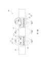
請參閱第1圖,其中第1圖繪示依照本發明第一實施例之一種磁性發光二極體晶粒移轉裝置100與磁性發光二極體晶粒L1的示意圖。依據本發明一實施方式提供一種磁性發光二極體晶粒移轉裝置100,用以移轉複數磁性發光二極體晶粒L1,各磁性發光二極體晶粒L1包含一N極L11及一S極L12並具有一高度方向,各N極L11及各S極L12的排列方向概與高度方向垂直,磁性發光二極體晶粒移轉裝置100包含一基板110、複數磁性件120以及一振動機構130。基板110包含複數晶粒設置區111,前述複數晶粒設置區111間隔排列,且各晶粒設置區111包含一設置面1111。各磁性件120與各晶粒設置區111對位,且各磁性件120包含一對位N極121及一對位S極122,各對位N極121與各對位S極122的排列方向概與各設置面1111平行,且一磁性件120的對位N極121對應相鄰之另一磁性件120的對位S極122。振動機構130耦合於基板110。其中,各磁性發光二極體晶粒L1的各N極L11及各S極L12分別用以被各對位S極122及各對位N極121吸引,以使各磁性發光二極體晶粒L1被移轉對位至各晶粒設置區111;當至少一磁性發光二極體晶粒L1落入一晶粒設置區111且前述至少一磁性發光二極體晶粒L1的N極L11未與前述一晶粒設置區111的磁性件120的對位S極122對位,則振動機構130使基板110振動以讓前述至少一磁性發光二極體晶粒L1翻轉並重新對位。Please refer to FIG. 1 , which is a schematic diagram of a magnetic light-emitting diode
藉此,基於磁性件120之對位N極121與對位S極122的排列方向關係,可透過異性相吸之原理確實吸引磁性發光二極體晶粒L1移轉對位,而能達到一次大量移轉之效果。並且,透過振動機構130使基板110振動,而能將未對位之磁性發光二極體晶粒L1翻轉,以再次對位,不僅具有使用方便性,更可提高對位效率。後面將詳述磁性發光二極體晶粒移轉裝置100的細節。In this way, based on the arrangement direction relationship between the
磁性發光二極體晶粒L1可以包含一磊晶層及一磁性金屬板,磊晶層設置於磁性金屬板上,磁性金屬板可例如包含一鎳鐵合金層及一銅層,而能具有高熱傳導係數、低熱膨脹係數和初始磁導率,且會具有微弱的磁性,並且磁性方向是水平排列。The magnetic light-emitting diode grain L1 may include an epitaxial layer and a magnetic metal plate. The epitaxial layer is disposed on the magnetic metal plate. The magnetic metal plate may include, for example, a nickel-iron alloy layer and a copper layer, which can have high thermal conductivity. coefficient, low thermal expansion coefficient and initial magnetic permeability, and will have weak magnetism, and the magnetic direction is horizontally aligned.
基板110可以是透明基板或絕緣基板,晶粒設置區111可具有凹槽結構,凹槽結構的底面即形成設置面1111,且各晶粒設置區111之間可以相隔一間隔區112。於第1圖的第一實施例中,各磁性件120可具有一磁鐵結構,其可以是埋設於基板110內,而在其他實施例中,各磁性件亦可以是設置於基板外,不以此為限。The
各磁性件120呈水平排列,磁性件120會產生磁力,於各設置面1111上方與下方的磁力線切線方向分別為D11與D12,而於各間隔區112的上方及下方亦會形成磁力線切線方向D21與D22。如第1圖所示,磁力線切線方向D11與磁力線切線方向D21相反並互斥,而能有助於分開磁性發光二極體晶粒L1。換句話說,因磁性發光二極體晶粒L1的磁性是水平排列,而會有水平吸引連接的困擾產生,即,磁性發光二極體晶粒L1容易彼此連接而不易分開。透過晶粒設置區111的磁力線切線方向D11與間隔區112的磁力線切線方向D21相反的配置,可有助於在磁性發光二極體晶粒L1轉移時分離連接之磁性發光二極體晶粒L1。The
振動機構130可以具有一振動桿結構,振動機構130內可設置馬達及偏心塊等元件來造成振動,而能振動基板110。在其他實施例中,基板可連接一機械手臂,並透過機械手臂來振動基板,不以此限制本發明。在磁性發光二極體晶粒L1轉移的過程中,可能會有部分的磁性發光二極體晶粒L1在落入晶粒設置區111時反置,即,磁性發光二極體晶粒L1的S極L12與磁性件120的對位S極122對位,如此因互斥關係導致磁性發光二極體晶粒L1無法被磁性件120吸附固定,而仍處於可活動的狀態。在此情況下,若是利用振動機構130上下振動基板110,則此些可活動的磁性發光二極體晶粒L1會被彈起、翻轉,並能重新對位。而方向正確且被磁性件120吸附固定的磁性發光二極體晶粒L1並不會受到影響,仍保持固定。The
此外,各磁性發光二極體晶粒L1的一底面可概呈正方形。也就是說,磁性發光二極體晶粒L1底面的長、寬均相同,故晶粒設置區111亦可以對應磁性發光二極體晶粒L1而具有長、寬相等之設置面1111,如此磁性發光二極體晶粒L1較容易落入晶粒設置區111。In addition, a bottom surface of each magnetic light-emitting diode die L1 may be substantially square. That is to say, the length and width of the bottom surface of the magnetic light-emitting diode grain L1 are the same, so the
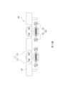
請參閱第2圖,其中第2圖繪示依照本發明第二實施例之一種磁性發光二極體晶粒移轉裝置200與磁性發光二極體晶粒L1的示意圖。第2圖第二實施例的磁性發光二極體晶粒移轉裝置200與第1圖第一實施例的磁性發光二極體晶粒移轉裝置100類似,但磁性件220是獨立於基板210之外,而磁性件220可具有一電磁鐵結構。如第2圖所示,磁性件220可纏繞線圈並通電,而能形成對位N極221及對位S極222,對位N極221及對位S極222水平排列,而與磁性發光二極體晶粒L1的N極L11及S極L12的排列方向相同,以達到吸附對位的效果。磁性件220的磁力大小可透過電流的大小或線圈匝數的多寡來達成,且磁極方向可透過電流方向改變,而更具有配置方便有優點。Please refer to FIG. 2 , which is a schematic diagram of a magnetic light-emitting diode die
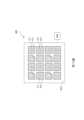
請參閱第3圖及第4圖,其中第3圖繪示依照本發明第三實施例之一種磁性發光二極體晶粒移轉裝置300與磁性發光二極體晶粒L1的部分側面剖視示意圖,第4圖繪示第3圖第三實施例之磁性發光二極體晶粒移轉裝置300的磁性件320的俯視示意圖。於磁性發光二極體晶粒移轉裝置300中,磁性件320亦具有電磁鐵結構,且各磁性件320包含一玻璃板323、複數第一貫通孔324、複數第二貫通孔325、複數第一導電部326及複數第二導電部327。玻璃板323設置在基板310下,前述複數第一貫通孔324貫穿玻璃板323且彼此等距排列。前述複數第二貫通孔325貫穿玻璃板323且彼此等距排列,前述複數第二貫通孔325與前述複數第一貫通孔324交錯排列但不共線。前述複數第一導電部326填充於各第一貫通孔324及各第二貫通孔325。前述複數第二導電部327位於玻璃板323的表面,且各第二導電部327連接位於各第一貫通孔324的各第一導電部326及位於各第二貫通孔325的各第一導電部326。其中,前述複數第一導電部326及前述複數第二導電部327連接形成螺旋狀結構。在此情況下,對位N極321及對位S極322是呈水平排列,而與磁性發光二極體晶粒L1的N極L11及S極L12排列方向相同,以達到吸附對位的效果。Please refer to Figures 3 and 4. Figure 3 shows a partial side cross-section of a magnetic light-emitting diode die
具體地,如第3圖及第4圖所示,玻璃板323可例如包含3個第一貫通孔324及3個第二貫通孔325,3個第一貫通孔324沿水平方向排成一列,3個第二貫通孔325沿水平方向排成另一列,且每個第一貫通孔324與每個第二貫通孔325於垂直方向不共線。第一導電部326及第二導電部327可例如為銅,也就是說,第一導電部326設置於第一貫通孔324及第二貫通孔325後,即形成導電孔(VIA)結構,而第二導電部327用以設置在玻璃板323的上表面及下表面,最後可形成螺旋狀的線圈結構,而經通電後可形成對位S極322及對位N極321。在第三實施例中,玻璃板323可更具有防止磁性件320短路的效果。請特別注意的是,雖第3圖及第4圖中所繪示之第一導電部326及第二導電部327形成的線圈匝數為3,仍可依磁力線需求改變線圈匝數,不以圖式為限。Specifically, as shown in Figures 3 and 4, the
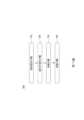
請參閱第5圖及第6圖,其中第5圖繪示依照本發明第四實施例之一種磁性發光二極體晶粒移轉裝置400與磁性發光二極體晶粒L1、L2、L3的俯視示意圖,第6圖繪示依照本發明第四實施例之磁性發光二極體晶粒移轉裝置400的基板410的形成圖。磁性發光二極體晶粒移轉裝置400的基板410可包含複數晶粒設置區411、412、413,晶粒設置區411、412、413分別用以設置磁性發光二極體晶粒L1、L2、L3,且磁性發光二極體晶粒L1可以發出第一色光例如紅光,磁性發光二極體晶粒L2可以發出第二色光例如藍光,而磁性發光二極體晶粒L3可以發出第三色光例如藍光。Please refer to Figures 5 and 6. Figure 5 illustrates a magnetic light-emitting diode die
如第5圖及第6圖及所示,基板410上可先形成多個通孔415,於基板410上塗佈光阻R1,再透過曝光及蝕刻而可形成複數金屬設置區416以分別連通前述複數通孔415。如此再於各金屬設置區416及各通孔415填充金屬材料M1,便可形成晶粒設置區411、412、413。在其他實施例中,基板亦可以使用其他方式形成,不以此為限。As shown in Figures 5 and 6, a plurality of through
請復參閱第5圖,各個晶粒設置區411、412、413可對應一磁性件(未於第四實施例中繪示),而磁性發光二極體晶粒移轉裝置400更包含一控制器440,其電性連接磁性件,控制器440用以控制各磁性件開啟以產生磁力,或關閉以取消磁力。換句話說,由於磁性件具有電磁鐵結構,因此可以透過開啟通電以產生磁力,而當未通電時,磁性件即不具有磁力,故可透過控制器440控制各磁性件,而選擇所需要的晶粒設置區411、412、413以設置所需要的磁性發光二極體晶粒L1、L2、L3。Please refer to Figure 5 again. Each die setting
舉例而言,可先開啟所有晶粒設置區411所對應之磁性件,取大量之磁性發光二極體晶粒L1,以使磁性發光二極體晶粒L1轉移吸附至晶粒設置區411;再開啟所有晶粒設置區411、412所對應之磁性件,取大量之磁性發光二極體晶粒L2,以使磁性發光二極體晶粒L2轉移吸附至晶粒設置區412;最後,打開所有晶粒設置區411、412、413所對應之磁性件,取大量之磁性發光二極體晶粒L3,以使磁性發光二極體晶粒L3轉移吸附至晶粒設置區413,包含上述揭露但不以此為限。For example, all the magnetic components corresponding to the
請參閱第7圖,並一併參閱第1圖,其中第7圖繪示依照本發明第五實施例之一種磁性發光二極體晶粒移轉方法500的方塊流程圖,以下將參照第1圖的磁性發光二極體晶粒移轉裝置100說明磁性發光二極體晶粒移轉方法500的細節。磁性發光二極體晶粒移轉方法500可用以移轉複數磁性發光二極體晶粒L1,各磁性發光二極體晶粒L1包含一N極L11及一S極L12並具有一高度方向,各N極L11及各S極L12的排列方向概與高度方向垂直,磁性發光二極體晶粒移轉方法500包含一基板提供步驟510、一磁性件提供步驟520、一移轉步驟530以及一振動步驟540。Please refer to Figure 7 and refer to Figure 1 together. Figure 7 illustrates a block flow chart of a magnetic light-emitting diode die
於基板提供步驟510中,提供一基板110,基板110包含複數晶粒設置區111。In the
於磁性件提供步驟520中,提供複數磁性件120分別對應前述複數晶粒設置區111,各磁性件120間隔排列於基板110內,各磁性件120包含一對位N極121及一對位S極122,各對位N極121與各對位S極122的排列方向概與各設置面1111平行,且一磁性件120的對位N極121對應相鄰之另一磁性件120的對位S極122。In the
於移轉步驟530中,使各磁性發光二極體晶粒L1的各N極L11及各S極L12分別用以被各對位S極122及各對位N極121吸引,以將各磁性發光二極體晶粒L1移轉對位至各晶粒設置區111。In the
於振動步驟540中,使基板110振動,將與至少一晶粒設置區111的磁性件120極性互斥之至少一磁性發光二極體晶粒L1翻轉,以使前述至少一磁性發光二極體晶粒L1重新對位。In the
具體地,於基板提供步驟510中,晶粒設置區111是間隔排列,且各晶粒設置區111具有凹槽結構並具有一容置空間。於磁性件提供步驟520中,磁性件120可以具有磁鐵結構,且可於製作基板110時即埋設於基板110內並對應各晶粒設置區111的設置面1111。或者,亦可以如第2圖的第二實施例,讓磁性件220具有電磁鐵結構,並且獨立於基板210外。Specifically, in the
於移轉步驟530中,可以提供大量的磁性發光二極體晶粒L1,在初始的狀態中,各磁性發光二極體晶粒L1未被受磁性件120磁力吸附而可能處於彼此連接且可任意移動的狀態。於移轉步驟530中,各磁性發光二極體晶粒L1受到磁性件120的磁力吸附,而落入各晶粒設置區111的容置空間,並且因磁力因素而無法任意活動。而若是各磁性發光二極體晶粒L1落入各晶粒設置區111的容置空間但方向反置,此時磁性發光二極體晶粒L1的磁力與磁性件120的磁力互斥,因此,可於振動步驟540,使基板110上下振動,如此可以使方向反置之磁性發光二極體晶粒L1脫離容置空間後再重新落入容置空間,而透過振動加上磁力相反的關係,有助於讓磁性發光二極體晶粒L1翻轉,進而有助於重新對位。In the
如第5圖至第7圖所示,可讓基板410由一玻璃材料製成,則基板提供步驟510可包含:於基板410上形成複數通孔415;於基板410上進行光阻R1塗佈、曝光及蝕刻,以於基板410上形成複數金屬設置區416以分別連通前述複數通孔415;以及於各金屬設置區416及各通孔415填充金屬材料M1以形成各晶粒設置區411、412、413。As shown in Figures 5 to 7, the
磁性發光二極體晶粒L1、L2、L3可發出不同色光,其中,磁性發光二極體晶粒L1發出第一色光,磁性發光二極體晶粒L2發出第二色光,且磁性發光二極體晶粒L3發出第三色光。因此,於移轉步驟530中,可先使磁性件中的一部分開啟,即,使晶粒設置區411所對應之磁性件通電,以產生磁力讓發出第一色光的磁性發光二極體晶粒L1被吸引對位;接著,維持前述複數磁性件中的前述一部分開啟,並使前述複數磁性件中的另一部分開啟,即,使與晶粒設置區411、412所對應之磁性件通電,以產生磁力讓發出第二色光的磁性發光二極體晶粒L2被吸引對位;最後,開啟所有之前述複數磁性件,即使所有晶粒設置區411、412、413所對應之磁性件通電,並讓發出第三色光的磁性發光二極體晶粒L3被吸引對位。如此可於不同之晶粒設置區411、412、413設置不同色光之磁性發光二極體晶粒L1、L2、L3。在此要特別注意的是,在設置磁性發光二極體晶粒L1時,若有未對位者,可進行振動步驟540,直到所有的磁性發光二極體晶粒L1均設置完成,再進行第二色光之磁性發光二極體晶粒L2,並且同樣可搭配振動步驟540,細節不再贅述。The magnetic light-emitting diode crystals L1, L2, and L3 can emit different colors of light. Among them, the magnetic light-emitting diode crystal L1 emits the first color light, the magnetic light-emitting diode crystal L2 emits the second color light, and the magnetic light-emitting diode crystal L2 emits the second color light. The polar body crystal L3 emits the third color light. Therefore, in the
雖然本發明已以實施例揭露如上,然其並非用以限定本發明,任何熟習此技藝者,在不脫離本發明之精神和範圍內,當可作各種之更動與潤飾,因此本發明之保護範圍當視後附之申請專利範圍所界定者為準。Although the present invention has been disclosed above through embodiments, they are not intended to limit the present invention. Anyone skilled in the art can make various modifications and modifications without departing from the spirit and scope of the present invention. Therefore, the protection of the present invention is The scope shall be determined by the appended patent application scope.
100,200,300,400:磁性發光二極體晶粒移轉裝置 110,210,310,410:基板 111,411,412,413:晶粒設置區 1111:設置面 112:間隔區 120,220,320:磁性件 121,221,321:對位N極 122,222,322:對位S極 130:振動機構 323:玻璃板 324:第一貫通孔 325:第二貫通孔 326:第一導電部 327:第二導電部 415:通孔 416:金屬設置區 440:控制器 500:磁性發光二極體晶粒移轉方法 510:基板提供步驟 520:磁性件提供步驟 530:移轉步驟 540:振動步驟 D11,D12,D21,D22:磁力線切線方向 L1,L2,L3:磁性發光二極體晶粒 L11:N極 L12:S極 M1:金屬材料 R1:光阻100, 200, 300, 400: Magnetic light emitting diode grain transfer device 110,210,310,410:Substrate 111,411,412,413: Die setting area 1111: Setting surface 112: spacer area 120,220,320: Magnetic parts 121,221,321: Counterposition N pole 122,222,322: Counterpoint S pole 130:Vibration mechanism 323:Glass plate 324: First through hole 325: Second through hole 326:First conductive part 327: Second conductive part 415:Through hole 416:Metal setting area 440:Controller 500: Magnetic light-emitting diode grain transfer method 510: Substrate provision step 520: Steps to provide magnetic parts 530:Transfer steps 540: Vibration step D11, D12, D21, D22: tangent direction of magnetic field lines L1, L2, L3: magnetic light-emitting diode grains L11: N pole L12: S pole M1: metal material R1: Photoresist
第1圖繪示依照本發明第一實施例之一種磁性發光二極體晶粒移轉裝置與磁性發光二極體晶粒的示意圖; 第2圖繪示依照本發明第二實施例之一種磁性發光二極體晶粒移轉裝置與磁性發光二極體晶粒的示意圖; 第3圖繪示依照本發明第三實施例之一種磁性發光二極體晶粒移轉裝置與磁性發光二極體晶粒的部分側面剖視示意圖; 第4圖繪示第3圖第三實施例之磁性發光二極體晶粒移轉裝置的磁性件的俯視示意圖; 第5圖繪示依照本發明第四實施例之一種磁性發光二極體晶粒移轉裝置與磁性發光二極體晶粒的俯視示意圖; 第6圖繪示依照本發明第四實施例之磁性發光二極體晶粒移轉裝置的基板的形成圖;以及 第7圖繪示依照本發明第五實施例之一種磁性發光二極體晶粒移轉方法的方塊流程圖。Figure 1 is a schematic diagram of a magnetic light-emitting diode grain transfer device and magnetic light-emitting diode grains according to the first embodiment of the present invention; Figure 2 is a schematic diagram of a magnetic light-emitting diode grain transfer device and magnetic light-emitting diode grains according to a second embodiment of the present invention; Figure 3 shows a partial side cross-sectional view of a magnetic light-emitting diode chip transfer device and magnetic light-emitting diode chips according to the third embodiment of the present invention; Figure 4 shows a schematic top view of the magnetic component of the magnetic light-emitting diode grain transfer device of the third embodiment of Figure 3; Figure 5 shows a schematic top view of a magnetic light-emitting diode grain transfer device and magnetic light-emitting diode grains according to the fourth embodiment of the present invention; Figure 6 shows a formation diagram of a substrate of a magnetic light-emitting diode die transfer device according to the fourth embodiment of the present invention; and FIG. 7 illustrates a block flow chart of a magnetic light-emitting diode grain transfer method according to the fifth embodiment of the present invention.
100:磁性發光二極體晶粒移轉裝置 110:基板 111:晶粒設置區 1111:設置面 112:間隔區 120:磁性件 121:對位N極 122:對位S極 130:振動機構 L1:磁性發光二極體晶粒 L11:N極 L12:S極 D11,D12,D21,D22:磁力線切線方向100: Magnetic light emitting diode grain transfer device 110:Substrate 111:Die setting area 1111: Setting surface 112: spacer area 120:Magnetic parts 121: Alignment N pole 122: Counterpoint S pole 130:Vibration mechanism L1: Magnetic light-emitting diode crystal grain L11: N pole L12: S pole D11, D12, D21, D22: tangent direction of magnetic field lines
Claims (10)
Translated fromChinesePriority Applications (3)
| Application Number | Priority Date | Filing Date | Title |
|---|---|---|---|
| TW111117614ATWI827047B (en) | 2022-05-11 | 2022-05-11 | Magnetic led die transferring device and magnetic led die transferring method |
| US18/190,116US20230369296A1 (en) | 2022-05-11 | 2023-03-26 | Magnetic led die transferring device and magnetic led die transferring method |
| JP2023078172AJP7535814B2 (en) | 2022-05-11 | 2023-05-10 | Magnetic light emitting diode die transfer device and magnetic light emitting diode die transfer method |
Applications Claiming Priority (1)
| Application Number | Priority Date | Filing Date | Title |
|---|---|---|---|
| TW111117614ATWI827047B (en) | 2022-05-11 | 2022-05-11 | Magnetic led die transferring device and magnetic led die transferring method |
Publications (2)
| Publication Number | Publication Date |
|---|---|
| TW202345421A TW202345421A (en) | 2023-11-16 |
| TWI827047Btrue TWI827047B (en) | 2023-12-21 |
Family
ID=88699514
Family Applications (1)
| Application Number | Title | Priority Date | Filing Date |
|---|---|---|---|
| TW111117614ATWI827047B (en) | 2022-05-11 | 2022-05-11 | Magnetic led die transferring device and magnetic led die transferring method |
Country Status (3)
| Country | Link |
|---|---|
| US (1) | US20230369296A1 (en) |
| JP (1) | JP7535814B2 (en) |
| TW (1) | TWI827047B (en) |
Citations (2)
| Publication number | Priority date | Publication date | Assignee | Title |
|---|---|---|---|---|
| TWM610443U (en)* | 2020-12-14 | 2021-04-11 | 晶呈科技股份有限公司 | Alignment module for magnetic light-emitting diode die transfer |
| TWI760007B (en)* | 2020-12-14 | 2022-04-01 | 晶呈科技股份有限公司 | Alignment module and alignment method for magnetic light emitting diode die transfer |
Family Cites Families (5)
| Publication number | Priority date | Publication date | Assignee | Title |
|---|---|---|---|---|
| US5824186A (en)* | 1993-12-17 | 1998-10-20 | The Regents Of The University Of California | Method and apparatus for fabricating self-assembling microstructures |
| JP4281044B2 (en)* | 2002-06-18 | 2009-06-17 | 財団法人名古屋産業科学研究所 | Micropart placement method |
| US9181630B2 (en)* | 2010-07-14 | 2015-11-10 | Sharp Kabushiki Kaisha | Method for disposing fine objects, apparatus for arranging fine objects, illuminating apparatus and display apparatus |
| JP2014090052A (en)* | 2012-10-30 | 2014-05-15 | Nichia Chem Ind Ltd | Light-emitting element, light-emitting device and light-emitting device manufacturing method |
| JP7092496B2 (en)* | 2017-12-22 | 2022-06-28 | 晶呈科技股▲分▼有限公司 | Structure of vertical light emitting diode die and its manufacturing method |
- 2022
- 2022-05-11TWTW111117614Apatent/TWI827047B/enactive
- 2023
- 2023-03-26USUS18/190,116patent/US20230369296A1/enactivePending
- 2023-05-10JPJP2023078172Apatent/JP7535814B2/enactiveActive
Patent Citations (2)
| Publication number | Priority date | Publication date | Assignee | Title |
|---|---|---|---|---|
| TWM610443U (en)* | 2020-12-14 | 2021-04-11 | 晶呈科技股份有限公司 | Alignment module for magnetic light-emitting diode die transfer |
| TWI760007B (en)* | 2020-12-14 | 2022-04-01 | 晶呈科技股份有限公司 | Alignment module and alignment method for magnetic light emitting diode die transfer |
Also Published As
| Publication number | Publication date |
|---|---|
| JP7535814B2 (en) | 2024-08-19 |
| JP2023168286A (en) | 2023-11-24 |
| TW202345421A (en) | 2023-11-16 |
| US20230369296A1 (en) | 2023-11-16 |
Similar Documents
| Publication | Publication Date | Title |
|---|---|---|
| CN109755162B (en) | Transfer device, Micro-LED crystal grain and transfer method | |
| US11342376B2 (en) | Light emitting diode, display substrate and transfer method | |
| CN111816751B (en) | Micro light-emitting diode display panel and preparation method thereof | |
| CN109378370B (en) | Transfer equipment of micro LED, manufacturing system and manufacturing method of display substrate | |
| TWI727368B (en) | Method for transferring light emitting elements, display panel, method for making the display panel, and substrate | |
| CN110416124B (en) | LED transfer method and LED display panel preparation method | |
| US6919581B2 (en) | Image display unit and production method thereof | |
| US6919007B2 (en) | Apparatus for mounting chips | |
| CN109065677A (en) | Micro-LED flood tide transfer method and Micro-LED substrate | |
| US10566125B2 (en) | Magnetic transfer module and method for transferring electronic element | |
| CN109300931A (en) | Micro LED display panel, manufacturing method and display device | |
| EP4084067A1 (en) | Apparatus and method of manufacturing display using light emitting element | |
| JP6600060B2 (en) | Method and system for mass arrangement of microcomponent devices | |
| CN110634906A (en) | A light emitting diode display | |
| KR20200026693A (en) | Method for manufacturing display device using semiconductor light emitting diode | |
| CN110416122B (en) | Transfer method of light-emitting element, display panel and preparation method thereof, substrate | |
| CN111244016B (en) | Transfer device, manufacturing method of transfer device, and transfer method | |
| TWI827047B (en) | Magnetic led die transferring device and magnetic led die transferring method | |
| CN110323309B (en) | Display panel manufacturing method and display panel manufacturing system | |
| CN115832125A (en) | Programmable transfer method for three-color micro-LED chips | |
| CN117334797B (en) | A flow magnetic self-assembly mass transfer device and transfer method | |
| CN117096084A (en) | Magnetic LED crystal grain transferring device and transferring method thereof | |
| CN116387177A (en) | Mass transfer device, mass transfer system and mass transfer method | |
| CN119092621A (en) | An integrated electromagnetic directional falling mechanism and process for magnetized rectangular LED chips |