TWI819249B - Reflective display apparatus and light guide module - Google Patents
Reflective display apparatus and light guide moduleDownload PDFInfo
- Publication number
- TWI819249B TWI819249BTW109137762ATW109137762ATWI819249BTW I819249 BTWI819249 BTW I819249BTW 109137762 ATW109137762 ATW 109137762ATW 109137762 ATW109137762 ATW 109137762ATW I819249 BTWI819249 BTW I819249B
- Authority
- TW
- Taiwan
- Prior art keywords
- light
- light guide
- reflective display
- edge
- microns
- Prior art date
Links
- 230000003287optical effectEffects0.000claimsabstractdescription44
- 239000011241protective layerSubstances0.000claimsdescription13
- 230000000052comparative effectEffects0.000description9
- 229920000089Cyclic olefin copolymerPolymers0.000description5
- 238000010586diagramMethods0.000description5
- 238000000034methodMethods0.000description4
- 229920003023plasticPolymers0.000description4
- 229920003229poly(methyl methacrylate)Polymers0.000description4
- 239000004926polymethyl methacrylateSubstances0.000description4
- 239000000758substrateSubstances0.000description4
- 238000005530etchingMethods0.000description2
- 239000011521glassSubstances0.000description2
- 238000005259measurementMethods0.000description2
- 238000012986modificationMethods0.000description2
- 230000004048modificationEffects0.000description2
- -1poly(methyl methacrylate)Polymers0.000description2
- 229920000515polycarbonatePolymers0.000description2
- 239000004417polycarbonateSubstances0.000description2
- 239000004986Cholesteric liquid crystals (ChLC)Substances0.000description1
- 239000004713Cyclic olefin copolymerSubstances0.000description1
- NIXOWILDQLNWCW-UHFFFAOYSA-Nacrylic acid groupChemical groupC(C=C)(=O)ONIXOWILDQLNWCW-UHFFFAOYSA-N0.000description1
- 230000001154acute effectEffects0.000description1
- 239000000853adhesiveSubstances0.000description1
- 230000001070adhesive effectEffects0.000description1
- 150000001925cycloalkenesChemical class0.000description1
- 239000010408filmSubstances0.000description1
- 239000010410layerSubstances0.000description1
- 238000004519manufacturing processMethods0.000description1
- 239000000463materialSubstances0.000description1
Images


Classifications
- G—PHYSICS
- G02—OPTICS
- G02B—OPTICAL ELEMENTS, SYSTEMS OR APPARATUS
- G02B6/00—Light guides; Structural details of arrangements comprising light guides and other optical elements, e.g. couplings
- G02B6/0001—Light guides; Structural details of arrangements comprising light guides and other optical elements, e.g. couplings specially adapted for lighting devices or systems
- G02B6/0011—Light guides; Structural details of arrangements comprising light guides and other optical elements, e.g. couplings specially adapted for lighting devices or systems the light guides being planar or of plate-like form
- G02B6/0033—Means for improving the coupling-out of light from the light guide
- G02B6/005—Means for improving the coupling-out of light from the light guide provided by one optical element, or plurality thereof, placed on the light output side of the light guide
- G02B6/0055—Reflecting element, sheet or layer
- G—PHYSICS
- G02—OPTICS
- G02B—OPTICAL ELEMENTS, SYSTEMS OR APPARATUS
- G02B6/00—Light guides; Structural details of arrangements comprising light guides and other optical elements, e.g. couplings
- G02B6/0001—Light guides; Structural details of arrangements comprising light guides and other optical elements, e.g. couplings specially adapted for lighting devices or systems
- G02B6/0011—Light guides; Structural details of arrangements comprising light guides and other optical elements, e.g. couplings specially adapted for lighting devices or systems the light guides being planar or of plate-like form
- G02B6/0033—Means for improving the coupling-out of light from the light guide
- G02B6/0058—Means for improving the coupling-out of light from the light guide varying in density, size, shape or depth along the light guide
- G02B6/0061—Means for improving the coupling-out of light from the light guide varying in density, size, shape or depth along the light guide to provide homogeneous light output intensity
- G—PHYSICS
- G02—OPTICS
- G02B—OPTICAL ELEMENTS, SYSTEMS OR APPARATUS
- G02B6/00—Light guides; Structural details of arrangements comprising light guides and other optical elements, e.g. couplings
- G02B6/0001—Light guides; Structural details of arrangements comprising light guides and other optical elements, e.g. couplings specially adapted for lighting devices or systems
- G02B6/0011—Light guides; Structural details of arrangements comprising light guides and other optical elements, e.g. couplings specially adapted for lighting devices or systems the light guides being planar or of plate-like form
- G02B6/0081—Mechanical or electrical aspects of the light guide and light source in the lighting device peculiar to the adaptation to planar light guides, e.g. concerning packaging
- G02B6/0086—Positioning aspects
- G02B6/0088—Positioning aspects of the light guide or other optical sheets in the package
- G—PHYSICS
- G02—OPTICS
- G02B—OPTICAL ELEMENTS, SYSTEMS OR APPARATUS
- G02B6/00—Light guides; Structural details of arrangements comprising light guides and other optical elements, e.g. couplings
- G02B6/0001—Light guides; Structural details of arrangements comprising light guides and other optical elements, e.g. couplings specially adapted for lighting devices or systems
- G02B6/0011—Light guides; Structural details of arrangements comprising light guides and other optical elements, e.g. couplings specially adapted for lighting devices or systems the light guides being planar or of plate-like form
- G02B6/0081—Mechanical or electrical aspects of the light guide and light source in the lighting device peculiar to the adaptation to planar light guides, e.g. concerning packaging
- G02B6/0093—Means for protecting the light guide
- G—PHYSICS
- G02—OPTICS
- G02B—OPTICAL ELEMENTS, SYSTEMS OR APPARATUS
- G02B6/00—Light guides; Structural details of arrangements comprising light guides and other optical elements, e.g. couplings
- G02B6/0001—Light guides; Structural details of arrangements comprising light guides and other optical elements, e.g. couplings specially adapted for lighting devices or systems
- G02B6/0011—Light guides; Structural details of arrangements comprising light guides and other optical elements, e.g. couplings specially adapted for lighting devices or systems the light guides being planar or of plate-like form
- G02B6/0013—Means for improving the coupling-in of light from the light source into the light guide
- G02B6/0015—Means for improving the coupling-in of light from the light source into the light guide provided on the surface of the light guide or in the bulk of it
- G02B6/002—Means for improving the coupling-in of light from the light source into the light guide provided on the surface of the light guide or in the bulk of it by shaping at least a portion of the light guide, e.g. with collimating, focussing or diverging surfaces
- G—PHYSICS
- G02—OPTICS
- G02B—OPTICAL ELEMENTS, SYSTEMS OR APPARATUS
- G02B6/00—Light guides; Structural details of arrangements comprising light guides and other optical elements, e.g. couplings
- G02B6/0001—Light guides; Structural details of arrangements comprising light guides and other optical elements, e.g. couplings specially adapted for lighting devices or systems
- G02B6/0011—Light guides; Structural details of arrangements comprising light guides and other optical elements, e.g. couplings specially adapted for lighting devices or systems the light guides being planar or of plate-like form
- G02B6/0033—Means for improving the coupling-out of light from the light guide
- G02B6/0035—Means for improving the coupling-out of light from the light guide provided on the surface of the light guide or in the bulk of it
- G02B6/0036—2-D arrangement of prisms, protrusions, indentations or roughened surfaces
- G—PHYSICS
- G02—OPTICS
- G02B—OPTICAL ELEMENTS, SYSTEMS OR APPARATUS
- G02B6/00—Light guides; Structural details of arrangements comprising light guides and other optical elements, e.g. couplings
- G02B6/0001—Light guides; Structural details of arrangements comprising light guides and other optical elements, e.g. couplings specially adapted for lighting devices or systems
- G02B6/0011—Light guides; Structural details of arrangements comprising light guides and other optical elements, e.g. couplings specially adapted for lighting devices or systems the light guides being planar or of plate-like form
- G02B6/0033—Means for improving the coupling-out of light from the light guide
- G02B6/005—Means for improving the coupling-out of light from the light guide provided by one optical element, or plurality thereof, placed on the light output side of the light guide
Landscapes
- Physics & Mathematics (AREA)
- General Physics & Mathematics (AREA)
- Optics & Photonics (AREA)
- Planar Illumination Modules (AREA)
- Devices For Indicating Variable Information By Combining Individual Elements (AREA)
- Push-Button Switches (AREA)
- Instrument Panels (AREA)
Abstract
Description
Translated fromChinese本發明是有關於一種顯示裝置,且特別是有關於一種反射式顯示裝置及其導光模組。The present invention relates to a display device, and in particular, to a reflective display device and its light guide module.
目前有的顯示裝置具有導光模組來導引光源所發出的光線,以使顯示裝置可以顯示明亮的影像,從而有助於使用者觀賞,其中上述顯示裝置大多採用多個發光二極體(Light Emitting Diode,LED)來作為光源。由於發光二極體(LED)通常具有指向性(directionality characteristic),因此各個發光二極體所發出的光束具有較小的發散角,以至於容易造成亮暗不均的影像,從而降低顯示裝置的影像品質。Currently, some display devices have light guide modules to guide the light emitted by the light source, so that the display device can display bright images, thereby facilitating user viewing. Most of the above-mentioned display devices use multiple light-emitting diodes ( Light Emitting Diode (LED) as the light source. Since light-emitting diodes (LEDs) usually have directionality characteristics, the light beams emitted by each light-emitting diode have a small divergence angle, which easily causes uneven light and dark images, thus reducing the efficiency of the display device. Image quality.
本發明至少一實施例提出一種導光模組,其有助於讓光線均勻出射,以減少或避免出現亮暗不均的影像。At least one embodiment of the present invention provides a light guide module that helps to uniformly emit light to reduce or avoid uneven light and dark images.
本發明至少一實施例還提出一種反射式顯示裝置,其包括上述導光模組。At least one embodiment of the present invention also provides a reflective display device, which includes the above-mentioned light guide module.
本發明至少一實施例所提出的導光模組適於配置在反射式顯示面板上,並包括導光板與遮光體。導光板具有第一表面、相對第一表面的第二表面以及形成於第一表面的光學結構,其中第一表面具有顯示區以及圍繞顯示區的邊緣區,而光學結構分布於顯示區。遮光體配置於第一表面上,並覆蓋邊緣區,其中遮光體具有一開口,而開口暴露顯示區。The light guide module proposed in at least one embodiment of the present invention is suitable for being disposed on a reflective display panel, and includes a light guide plate and a light shielding body. The light guide plate has a first surface, a second surface opposite to the first surface, and an optical structure formed on the first surface. The first surface has a display area and an edge area surrounding the display area, and the optical structures are distributed in the display area. The light-shielding body is disposed on the first surface and covers the edge area, wherein the light-shielding body has an opening, and the opening exposes the display area.
在本發明至少一實施例中,上述光學結構不分布於邊緣區,而遮光體更覆蓋鄰近邊緣區的部分光學結構,其中光學結構具有被遮光體覆蓋的邊緣,而開口具有鄰近邊緣的側壁。此外,上述邊緣與側壁之間的距離小於或等於1公厘。In at least one embodiment of the present invention, the above-mentioned optical structures are not distributed in the edge area, and the light-shielding body further covers part of the optical structure adjacent to the edge area, wherein the optical structure has an edge covered by the light-shielding body, and the opening has a sidewall adjacent to the edge. In addition, the distance between the edge and the side wall is less than or equal to 1 mm.
在本發明至少一實施例中,上述光學結構包括多個凹槽,而各個凹槽從第一表面朝向第二表面延伸。In at least one embodiment of the present invention, the optical structure includes a plurality of grooves, and each groove extends from the first surface toward the second surface.
在本發明至少一實施例中,上述遮光體的厚度介於5微米至20微米之間。In at least one embodiment of the present invention, the thickness of the light shielding body is between 5 microns and 20 microns.
在本發明至少一實施例中,上述導光板還具有入光部。入光部連接在第一表面與第二表面之間,並具有多個外凸柱面與多個內凹柱面,其中這些外凸柱面與這些內凹柱面彼此交錯排列。In at least one embodiment of the present invention, the above-mentioned light guide plate further has a light incident portion. The light incident portion is connected between the first surface and the second surface, and has a plurality of outer convex cylinder surfaces and a plurality of inner concave cylinder surfaces, wherein the outer convex cylinder surfaces and the inner concave cylinder surfaces are staggered with each other.
在本發明至少一實施例中,各面外凸柱面的寬度與各面內凹柱面的寬度相等。In at least one embodiment of the present invention, the width of each out-of-plane convex cylinder is equal to the width of each in-plane concave cylinder.
在本發明至少一實施例中,相鄰兩面外凸柱面的中心軸之間的距離介於35微米至70微米之間。In at least one embodiment of the present invention, the distance between the central axes of two adjacent outer convex cylinder surfaces is between 35 microns and 70 microns.
在本發明至少一實施例中,各面外凸柱面具有波峰部,而各面內凹柱面具有一波谷部,其中入光部在波峰部與波谷部之間的厚度介於5微米至35微米之間。In at least one embodiment of the present invention, each out-of-plane convex cylindrical surface has a crest portion, and each in-plane concave cylindrical surface has a trough portion, wherein the thickness of the light incident portion between the crest portion and the trough portion is between 5 microns and between 35 microns.
本發明至少一實施例所提出的反射式顯示裝置包括反射式顯示面板、上述導光模組與多個發光元件。導光模組配置於反射式顯示面板上,並具有第一表面、相對第一表面的第二表面、形成於第一表面的光學結構以及連接在第一表面與第二表面之間的入光部。這些發光元件配置於入光部,其中各個發光元件用於朝向入光部發出光線。A reflective display device according to at least one embodiment of the present invention includes a reflective display panel, the above-mentioned light guide module and a plurality of light-emitting elements. The light guide module is disposed on the reflective display panel and has a first surface, a second surface opposite to the first surface, an optical structure formed on the first surface, and an incident light connected between the first surface and the second surface. department. These light-emitting elements are arranged in the light-incident part, and each light-emitting element is used to emit light toward the light-incident part.
在本發明至少一實施例中,上述反射式顯示裝置還包括保護層,其中保護層覆蓋導光模組,且導光模組位於保護層與反射式顯示面板之間。In at least one embodiment of the present invention, the above-mentioned reflective display device further includes a protective layer, wherein the protective layer covers the light guide module, and the light guide module is located between the protective layer and the reflective display panel.
利用上述光學結構,導光模組能幫助發光元件的光線從導光板均勻出射,以減少或避免出現亮暗不均的影像。Utilizing the above-mentioned optical structure, the light guide module can help the light of the light-emitting element emit evenly from the light guide plate to reduce or avoid uneven bright and dark images.
在以下的內文中,為了清楚呈現本案的技術特徵,圖式中的元件(例如層、膜、基板以及區域等)的尺寸(例如長度、寬度、厚度與深度)會以不等比例的方式放大。因此,下文實施例的說明與解釋不受限於圖式中的元件所呈現的尺寸與形狀,而應涵蓋如實際製程及/或公差所導致的尺寸、形狀以及兩者的偏差。例如,圖式所示的平坦表面可以具有粗糙及/或非線性的特徵,而圖式所示的銳角可以是圓的。所以,本案圖式所呈示的元件主要是用於示意,並非旨在精準地描繪出元件的實際形狀,也非用於限制本案的申請專利範圍。In the following text, in order to clearly present the technical features of this case, the dimensions (such as length, width, thickness and depth) of the components (such as layers, films, substrates, regions, etc.) in the drawings will be exaggerated in varying proportions. . Therefore, the description and explanation of the embodiments below are not limited to the sizes and shapes of the components in the drawings, but should cover the size, shape, and deviations in both caused by actual manufacturing processes and/or tolerances. For example, flat surfaces shown in the drawings may have rough and/or non-linear features, while acute angles shown in the drawings may be rounded. Therefore, the components shown in the drawings of this case are mainly for illustration and are not intended to accurately depict the actual shapes of the components, nor are they intended to limit the patent scope of this case.
其次,本案內容中所出現的「約」、「近似」或「實質上」等這類用字不僅涵蓋明確記載的數值與數值範圍,而且也涵蓋發明所屬技術領域中具有通常知識者所能理解的可允許偏差範圍,其中此偏差範圍可由測量時所產生的誤差來決定,而此誤差例如是起因於測量系統或製程條件兩者的限制。舉例而言,兩物件(例如基板的平面或走線)「實質上平行」或「實質上垂直」,其中「實質上平行」與「實質上垂直」分別代表這兩物件之間的平行與垂直可包括允許偏差範圍所導致的不平行與不垂直。Secondly, the words "about", "approximately" or "substantially" appearing in the content of this case not only cover the clearly stated numerical values and numerical ranges, but also cover what can be understood by a person with ordinary knowledge in the technical field to which the invention belongs. The allowable deviation range, where the deviation range can be determined by the error generated during measurement, and this error is caused, for example, by limitations of the measurement system or process conditions. For example, two objects (such as the plane or traces of a substrate) are "substantially parallel" or "substantially perpendicular", where "substantially parallel" and "substantially perpendicular" respectively represent the parallelism and perpendicularity between the two objects. It can include non-parallelism and non-perpendicularity caused by the allowable deviation range.
此外,「約」可表示在上述數值的一個或多個標準偏差內,例如±30%、±20%、±10%或±5%內。本案文中所出現的「約」、「近似」或「實質上」等這類用字可依光學性質、蝕刻性質、機械性質或其他性質來選擇可以接受的偏差範圍或標準偏差,並非單以一個標準偏差來套用以上光學性質、蝕刻性質、機械性質以及其他性質等所有性質。In addition, "about" may mean within one or more standard deviations of the above numerical value, such as within ±30%, ±20%, ±10%, or ±5%. Words such as "approximately", "approximately" or "substantially" appearing in this text can be used to select acceptable deviation ranges or standard deviations based on optical properties, etching properties, mechanical properties or other properties, and are not solely based on one The standard deviation applies to all the above optical properties, etching properties, mechanical properties and other properties.
圖1A是本發明至少一實施例的反射式顯示裝置的俯視示意圖,而圖1B是圖1A中沿線1B-1B剖面而繪製的剖面示意圖。請參閱圖1A與圖1B,反射式顯示裝置100包括反射式顯示面板110、多個發光元件120以及導光模組200,其中反射式顯示面板110可為電泳式顯示面板、電濕潤式顯示面板或膽固醇液晶顯示面板,而發光元件120例如是發光二極體。FIG. 1A is a schematic top view of a reflective display device according to at least one embodiment of the present invention, and FIG. 1B is a schematic cross-sectional view drawn along
導光模組200可以配置於反射式顯示面板110上,而這些發光元件120配置於導光模組200的同一側或依照需求配置於不同側。反射式顯示面板110可以利用光學膠(Optically Clear Adhesive,OCA,未繪示)黏合於導光模組200,或其他方式以使反射式顯示面板110被固定在導光模組200下方。The
導光模組200包括導光板210,其中導光板210為透明基板,其例如是玻璃板或透明塑膠板,其中此透明塑膠板的材料可以是聚甲基丙烯酸甲酯(Poly(methyl methacrylate),PMMA,也就是壓克力)、聚碳酸酯(Polycarbonate,PC)、環烯烴共聚物(Cyclo Olefin Coplymer,COC)或環烯烴聚合物(Cyclo Olefin Polymers,COP)。The
導光板210具有第一表面211a、相對第一表面211a的第二表面211b以及形成於第一表面211a的光學結構212,其中第二表面211b位於第一表面211a與反射式顯示面板110之間。因此,光學結構212形成於導光板210遠離反射式顯示面板110的一側(即第一表面211a),且未形成於導光板210鄰近反射式顯示面板110的一側(即第二表面211b)。The
第一表面211a具有顯示區A11以及圍繞顯示區A11的邊緣區A12,其中邊緣區A12鄰接顯示區A11。圖1A以虛線框表示邊緣區A12與顯示區A11之間的邊界(boundary),其中顯示區A11位於虛線框內,而邊緣區A12位於虛線框外。反射式顯示面板110所產生的影像主要顯示於顯示區A11,而光學結構212分布於顯示區A11,但不分布於邊緣區A12。The
光學結構212可以包括多個凹槽212a,其中各個凹槽212a從第一表面211a朝向第二表面211b延伸。從圖1B來看,各個凹槽212a的深度明顯小於導光板210的厚度,其中導光板210的厚度相當於第一表面211a與第二表面211b之間的距離。因此,各個凹槽212a不是貫穿導光板210而形成。The
在本實施例中,各個凹槽212a於第一表面211a的截面形狀可以是圓形(如圖1A所示)。然而,在其他實施例中,各個凹槽212a於第一表面211a的截面形狀可以是三角形、矩形、五邊形、六邊形或橢圓形。或者,這些凹槽212a於第一表面211a的截面形狀可包括多種幾何形狀,例如三角形、矩形、圓形、橢圓形、五邊形與六邊形其中至少兩種。此外,這些凹槽212a至少一者可以是條狀的溝槽,例如V形切槽(V-cut)。In this embodiment, the cross-sectional shape of each
其次,在本實施例中,這些凹槽212a可以隨機分布於第一表面211a,即這些凹槽212a可以呈不規則排列,如圖1A所示。然而,在其他實施例中,這些凹槽212a可以呈規則排列,例如陣列排列。因此,圖1A與圖1B僅供舉例說明,並非限制這些凹槽212a的形狀與排列。Secondly, in this embodiment, the
遮光體220配置於第一表面211a上,並覆蓋邊緣區A12,其中遮光體220具有開口221,而開口221暴露顯示區A11。遮光體220可以是由油墨所形成,且具有較薄的厚度T22,其例如可以介於5微米至20微米之間。因此,當使用者以大視角觀賞反射式顯示裝置100所顯示的影像時,使用者不易看到遮光體220,以避免反射式顯示裝置100的影像品質因受到遮光體220的影響而降低。此外,遮光體220可接觸於導光板210的第一表面211a。The
由於光學結構212不分布於邊緣區A12,因此遮光體220基本上不覆蓋光學結構212。然而,受限於製程公差的影響,在實際情況中,遮光體220可能會更覆蓋鄰近邊緣區A12的部分光學結構212,即遮光體220會覆蓋至少一個凹槽212a。以圖1A與圖1B為例,遮光體220會覆蓋一些鄰近邊緣區A12的凹槽212a。Since the
光學結構212具有被遮光體220覆蓋的邊緣,其中此邊緣為整個光學結構212的外緣。以本實施例為例,此邊緣可以相當於顯示區A11的邊緣,即邊緣區A12與顯示區A11之間的邊界(如圖1A所示的虛線框)。或者,在其他實施例中,此邊緣也可以是被遮光體220覆蓋的最外圍凹槽212a的邊緣。The
遮光體220的開口221具有鄰近上述邊緣(例如圖1A中的邊緣區A12與顯示區A11之間的邊界)的側壁S22。基於現有的製程公差,邊緣與側壁S22之間的距離D22可以控制在小於或等於1公厘,以使遮光體220僅覆蓋極少部分的光學結構212。如此,遮光體220實質上不覆蓋光學結構212。The
導光板210還具有入光部213與相對於入光部213的對向側214,其中入光部213與對向側214皆連接在第一表面211a與第二表面211b之間。在本實施例中,入光部213與對向側214皆可為導光板210的兩相對側平面。這些發光元件120配置於入光部213,其中各個發光元件120能朝向入光部213發出光線L1,以使光線L1能從入光部213進入導光板210內。The
當光線L1在導光板210內傳遞時,光線L1可以被位於第二表面211b的反射式顯示面板110反射至光學結構212。當光線L1入射至光學結構212時,這些凹槽212a能減少對光線L1的全反射(Total internal reflection),促使大部分的光線L1從第一表面211a出射。此外,光學結構212還能使這些發光元件120所發出的光線L1均勻地從第一表面211a出射,以減少或避免出現亮暗不均的影像,從而維持或提升反射式顯示裝置100的影像品質。When the light L1 is transmitted in the
在本實施例中,反射式顯示裝置100可以還包括保護層130,其中保護層130可以是透明基板,例如玻璃板或透明塑膠板,而透明塑膠板的材料可以是聚甲基丙烯酸甲酯(PMMA)、聚碳酸酯(PC)、環烯烴共聚物(COC)或環烯烴聚合物(COP)。保護層130覆蓋導光模組200的導光板210,所以導光模組200會位於保護層130與反射式顯示面板110之間。保護層130能保護導光模組200,以防止導光板210與遮光體220被撞傷或刮傷。In this embodiment, the
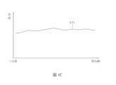
圖1C是圖1A中的反射式顯示裝置的亮度分布示意圖。請參閱圖1B與圖1C,在圖1C中,縱軸代表亮度,而橫軸代表導光板210的位置,其中左端代表入光部213的位置,而右端代表對向側214的位置。數線C11代表反射式顯示裝置100從入光部213至對向側214的亮度分布。從圖1C來看,數線C11沒有大幅度起伏,因此這些發光元件120所發出的光線L1能從第一表面211a均勻出射,以使反射式顯示裝置100的影像亮度均勻而不會出現亮暗不均的影像。FIG. 1C is a schematic diagram of the brightness distribution of the reflective display device in FIG. 1A . Please refer to FIG. 1B and FIG. 1C. In FIG. 1C, the vertical axis represents the brightness, and the horizontal axis represents the position of the
圖1D是圖1A中的反射式顯示裝置與對照例反射式顯示裝置兩者亮度分布的比較示意圖。請參閱圖1B與圖1D,與圖1C相同,在圖1D中,縱軸代表亮度,橫軸代表導光板210的位置,其中左端代表入光部213的位置,而右端代表對向側214的位置。數線C10(以虛線表示)代表對照例反射式顯示裝置的亮度分布,而數線C11代表反射式顯示裝置100的亮度分布。FIG. 1D is a schematic diagram comparing the brightness distribution of the reflective display device in FIG. 1A and the reflective display device of the comparative example. Please refer to FIG. 1B and FIG. 1D. It is the same as FIG. 1C. In FIG. 1D, the vertical axis represents the brightness, the horizontal axis represents the position of the
對照例反射式顯示裝置與反射式顯示裝置100兩者相似,而兩者之間的唯一差異僅在於:在對照例反射式顯示裝置中,光學結構212不僅分布於顯示區A11,而且更分布於邊緣區A12。換句話說,對照例反射式顯示裝置的光學結構212是全面性地分布於第一表面211a。相較於反射式顯示裝置100,對照例反射式顯示裝置的遮光體220覆蓋較多光學結構212,例如覆蓋較多凹槽212a。The comparative reflective display device is similar to the
從圖1D的數線C10來看,對照例反射式顯示裝置在其入光部213附近具有明顯偏高的亮度,以至於對照例反射式顯示裝置的入光部213附近會產生明顯的亮紋,導致影像品質下降。反之,反射式顯示裝置100各處的亮度彼此相差不大,即反射式顯示裝置100的影像亮度均勻。由此可知,減少或避免遮光體220對光學結構212的覆蓋有助於均勻化反射式顯示裝置100的影像亮度,以維持或提升反射式顯示裝置100的影像品質。Judging from the number line C10 in FIG. 1D , the reflective display device of the comparative example has significantly higher brightness near the
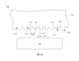
圖2A是本發明另一實施例的反射式顯示裝置的局部俯視示意圖,而圖2B是圖2A中的導光板的局部立體示意圖。請參閱圖2A與圖2B,反射式顯示裝置400與反射式顯示裝置100相似。例如,反射式顯示裝置400包括導光板310,而導光板310具有第一表面211a、第二表面211b、光學結構212(圖2A與圖2B未繪示)與入光部313,其中入光部313連接在第一表面211a與第二表面211b之間,而發光元件120配置於入光部313。FIG. 2A is a partial top view of a reflective display device according to another embodiment of the present invention, and FIG. 2B is a partial three-dimensional view of the light guide plate in FIG. 2ASchematic diagram. Referring to FIG. 2A and FIG. 2B , the
反射式顯示裝置100與400兩者唯一差異僅在於:入光部313不是平面,並具有多個外凸柱面313p與多個內凹柱面313r。這些外凸柱面313p與這些內凹柱面313r彼此交錯排列,以使這些外凸柱面313p與這些內凹柱面313r形成波浪面,其中這些外凸柱面313p與這些內凹柱面313r可以沿著第一表面211a與第二表面211b兩者的邊緣而排列。以圖2A為例,這些交錯排列的外凸柱面313p與內凹柱面313r會形成正弦波形狀的曲面,其中各面外凸柱面313p的寬度W3p與各面內凹柱面313r的寬度W3r相等,而相鄰兩面外凸柱面313p的中心軸A31之間的距離D30可以介於35微米至70微米之間。The only difference between the
此外,各面外凸柱面313p具有波峰部U31,而各面內凹柱面313r具有波谷部D31,其中入光部313在波峰部U31與波谷部D31之間的厚度T31可以介於5微米至35微米之間。利用這些外凸柱面313p與這些內凹柱面313r,入光部313能將發光元件120所發出的光線發散,以減少或避免亮暗不均的影像,從而維持或提升反射式顯示裝置400的影像品質。In addition, each out-of-plane convex
綜上所述,利用上述光學結構,本發明至少一實施例的導光模組能幫助發光元件的光線從導光板的第一表面均勻出射,以減少或避免出現亮暗不均的影像,進而提升反射式顯示裝置的影像品質。To sum up, using the above optical structure, the light guide module of at least one embodiment of the present invention can help the light of the light-emitting element to emit uniformly from the first surface of the light guide plate, so as to reduce or avoid the appearance of uneven bright and dark images, and thus Improve the image quality of reflective display devices.
雖然本發明已以實施例揭露如上,然其並非用以限定本發明,本發明所屬技術領域中具有通常知識者,在不脫離本發明精神和範圍內,當可作些許更動與潤飾,因此本發明保護範圍當視後附的申請專利範圍所界定者為準。Although the present invention has been disclosed above through embodiments, they are not intended to limit the present invention. Those with ordinary skill in the technical field to which the present invention belongs may make some modifications and modifications without departing from the spirit and scope of the present invention. Therefore, the present invention is The scope of invention protection shall be determined by the appended patent application scope.
100、400:反射式顯示裝置100, 400: Reflective display device
110:反射式顯示面板110: Reflective display panel
120:發光元件120:Light-emitting component
130:保護層130:Protective layer
200:導光模組200:Light guide module
210、310:導光板210, 310: Light guide plate
211a:第一表面211a: First surface
211b:第二表面211b: Second surface
212:光學結構212: Optical structure
212a:凹槽212a: Groove
213、313:入光部213, 313: light entrance part
214:對向側214: Opposite side
220:遮光體220:Light shield
221:開口221:Open your mouth
313p:外凸柱面313p:External convex cylinder
313r:內凹柱面313r: concave cylinder
A11:顯示區A11:Display area
A12:邊緣區A12: Edge area
A31:中心軸A31:Central axis
C10、C11:數線C10, C11: number line
D22、D30:距離D22, D30: distance
D31:波谷部D31: Trough part
L1:光線L1:Light
S22:側壁S22:Side wall
T22、T31:厚度T22, T31: Thickness
U31:波峰部U31:Crest part
W3p、W3r:寬度W3p, W3r: width
圖1A是本發明至少一實施例的反射式顯示裝置的俯視示意圖。 圖1B是圖1A中沿線1B-1B剖面而繪製的剖面示意圖。 圖1C是圖1A中的反射式顯示裝置的亮度分布示意圖。 圖1D是圖1A中的反射式顯示裝置與對照例反射式顯示裝置兩者亮度分布的比較示意圖。 圖2A是本發明另一實施例的反射式顯示裝置的局部俯視示意圖。 圖2B是圖2A中的導光板的局部立體示意圖。FIG. 1A is a schematic top view of a reflective display device according to at least one embodiment of the present invention. FIG. 1B is a schematic cross-sectional view taken along
100:反射式顯示裝置100: Reflective display device
110:反射式顯示面板110: Reflective display panel
120:發光元件120:Light-emitting component
130:保護層130:Protective layer
200:導光模組200:Light guide module
210:導光板210:Light guide plate
211a:第一表面211a: First surface
211b:第二表面211b: Second surface
212:光學結構212: Optical structure
212a:凹槽212a: Groove
213:入光部213: Light entrance part
214:對向側214: Opposite side
220:遮光體220:Light shield
221:開口221:Open your mouth
A11:顯示區A11:Display area
A12:邊緣區A12: Edge area
D22:距離D22: distance
L1:光線L1:Light
S22:側壁S22:Side wall
T22:厚度T22:Thickness
Claims (11)
Translated fromChinesePriority Applications (2)
| Application Number | Priority Date | Filing Date | Title |
|---|---|---|---|
| TW109137762ATWI819249B (en) | 2020-10-30 | 2020-10-30 | Reflective display apparatus and light guide module |
| US17/368,849US11460625B2 (en) | 2020-10-30 | 2021-07-07 | Reflective display apparatus and light guide module |
Applications Claiming Priority (1)
| Application Number | Priority Date | Filing Date | Title |
|---|---|---|---|
| TW109137762ATWI819249B (en) | 2020-10-30 | 2020-10-30 | Reflective display apparatus and light guide module |
Publications (2)
| Publication Number | Publication Date |
|---|---|
| TW202217413A TW202217413A (en) | 2022-05-01 |
| TWI819249Btrue TWI819249B (en) | 2023-10-21 |
Family
ID=81379968
Family Applications (1)
| Application Number | Title | Priority Date | Filing Date |
|---|---|---|---|
| TW109137762ATWI819249B (en) | 2020-10-30 | 2020-10-30 | Reflective display apparatus and light guide module |
Country Status (2)
| Country | Link |
|---|---|
| US (1) | US11460625B2 (en) |
| TW (1) | TWI819249B (en) |
Families Citing this family (1)
| Publication number | Priority date | Publication date | Assignee | Title |
|---|---|---|---|---|
| TWI843369B (en)* | 2022-12-29 | 2024-05-21 | 元太科技工業股份有限公司 | Display module |
Citations (5)
| Publication number | Priority date | Publication date | Assignee | Title |
|---|---|---|---|---|
| US20130063969A1 (en)* | 2011-08-19 | 2013-03-14 | Barnesandnoble.Com Llc | Planar front illumination system having a light guide with micro lenses formed thereon and method of manufacturing the same |
| TW201543118A (en)* | 2014-05-05 | 2015-11-16 | Au Optronics Corp | Back light module and display device |
| TW201831931A (en)* | 2017-02-16 | 2018-09-01 | 茂林光電科技股份有限公司 | A light guide plate, processing apparatus and processing method thereof |
| TW201833883A (en)* | 2017-03-02 | 2018-09-16 | 元太科技工業股份有限公司 | Cover plate structure and display device |
| TW202037982A (en)* | 2019-04-11 | 2020-10-16 | 大陸商蘇州璨鴻光電有限公司 | Display apparatus |
Family Cites Families (11)
| Publication number | Priority date | Publication date | Assignee | Title |
|---|---|---|---|---|
| US7969531B1 (en) | 2007-03-08 | 2011-06-28 | Jabil Circuit, Inc. | Integrated multi-function light guide for LCD backlighting |
| WO2010117115A1 (en)* | 2009-04-09 | 2010-10-14 | Lg Electronics Inc. | Display apparatus |
| KR20120048669A (en)* | 2009-08-03 | 2012-05-15 | 퀄컴 엠이엠에스 테크놀로지스, 인크. | Microstructures for light guide illumination |
| WO2013028467A1 (en)* | 2011-08-19 | 2013-02-28 | Barnesandnoble.Com Llc | Planar front illumination system having a light guide with micro scattering features formed thereon and method of manufacturing the same |
| US9261641B2 (en) | 2013-03-25 | 2016-02-16 | 3M Innovative Properties Company | Dual-sided film with compound prisms |
| TWI622837B (en) | 2013-10-24 | 2018-05-01 | 元太科技工業股份有限公司 | Display apparatus |
| CN105805640B (en)* | 2015-01-14 | 2019-10-18 | 元太科技工业股份有限公司 | front light module and display module |
| CN207216222U (en)* | 2017-10-12 | 2018-04-10 | 京东方科技集团股份有限公司 | A kind of backlight module and display device |
| CN108627908A (en) | 2018-05-11 | 2018-10-09 | 厦门光莆电子股份有限公司 | Modular light conducting plate |
| CN110568657A (en) | 2018-06-05 | 2019-12-13 | 中强光电股份有限公司 | display device |
| TWI707187B (en) | 2019-07-03 | 2020-10-11 | 元太科技工業股份有限公司 | Light guide module and display module having the same |
- 2020
- 2020-10-30TWTW109137762Apatent/TWI819249B/enactive
- 2021
- 2021-07-07USUS17/368,849patent/US11460625B2/enactiveActive
Patent Citations (5)
| Publication number | Priority date | Publication date | Assignee | Title |
|---|---|---|---|---|
| US20130063969A1 (en)* | 2011-08-19 | 2013-03-14 | Barnesandnoble.Com Llc | Planar front illumination system having a light guide with micro lenses formed thereon and method of manufacturing the same |
| TW201543118A (en)* | 2014-05-05 | 2015-11-16 | Au Optronics Corp | Back light module and display device |
| TW201831931A (en)* | 2017-02-16 | 2018-09-01 | 茂林光電科技股份有限公司 | A light guide plate, processing apparatus and processing method thereof |
| TW201833883A (en)* | 2017-03-02 | 2018-09-16 | 元太科技工業股份有限公司 | Cover plate structure and display device |
| TW202037982A (en)* | 2019-04-11 | 2020-10-16 | 大陸商蘇州璨鴻光電有限公司 | Display apparatus |
Also Published As
| Publication number | Publication date |
|---|---|
| US11460625B2 (en) | 2022-10-04 |
| TW202217413A (en) | 2022-05-01 |
| US20220137283A1 (en) | 2022-05-05 |
Similar Documents
| Publication | Publication Date | Title |
|---|---|---|
| US7649590B2 (en) | Backlight assembly and liquid crystal display having the same | |
| US10964918B1 (en) | Display screen and terminal | |
| TWI807032B (en) | Side-edge type surface light emitting apparatus having light guide plate sandwiched by upper and lower prism sheets | |
| US20120020078A1 (en) | Surface light source device | |
| TW202331374A (en) | Optical film and back light unit including the same | |
| WO2009128164A1 (en) | Optical device, uniform illumination device, optical sheet, backlight unit, and display unit | |
| US20160187564A1 (en) | Display device including optical member having optical patterns | |
| JP5175956B2 (en) | Light emitting device and display device | |
| TW202219603A (en) | Back light unit | |
| WO2021042283A1 (en) | Line recognition device and display device | |
| US8118469B2 (en) | Surface illuminating device and image display apparatus | |
| WO2016077309A2 (en) | Contrast enhancement sheet and display device comprising the same | |
| TWI819249B (en) | Reflective display apparatus and light guide module | |
| JP4321659B1 (en) | Optical device, optical uniform device, optical sheet, backlight unit and display device | |
| CN106526970B (en) | Liquid crystal display device | |
| CN114442214A (en) | Reflective display device and light guide module thereof | |
| KR20250134587A (en) | Edge-light type backlight unit, liquid crystal display, and information device | |
| JP7236801B2 (en) | Protective sheet for polarizing plate, polarizing plate, and liquid crystal display device | |
| US11487056B2 (en) | Light guide plate and backlight module using the same | |
| WO2022196162A1 (en) | Light diffusion sheet, backlight unit, liquid crystal display device, and information equipment | |
| CN116300170A (en) | display device | |
| TW202221393A (en) | Display apparatus and holder thereof | |
| TWI892165B (en) | Micro-structure film and light emitting module | |
| US20250028203A1 (en) | Backlight module | |
| KR101250375B1 (en) | Reflector patterned reflect film |