TWI818806B - Wafer bonding method - Google Patents
Wafer bonding methodDownload PDFInfo
- Publication number
- TWI818806B TWI818806BTW111144128ATW111144128ATWI818806BTW I818806 BTWI818806 BTW I818806BTW 111144128 ATW111144128 ATW 111144128ATW 111144128 ATW111144128 ATW 111144128ATW I818806 BTWI818806 BTW I818806B
- Authority
- TW
- Taiwan
- Prior art keywords
- temperature
- wafer
- adhesive layer
- component
- adhesive
- Prior art date
Links
- 238000000034methodMethods0.000titleclaimsabstractdescription99
- 239000012790adhesive layerSubstances0.000claimsabstractdescription131
- 235000012431wafersNutrition0.000claimsdescription235
- 239000000853adhesiveSubstances0.000claimsdescription66
- 230000001070adhesive effectEffects0.000claimsdescription66
- 230000007704transitionEffects0.000claimsdescription33
- 239000010410layerSubstances0.000claimsdescription11
- 238000006243chemical reactionMethods0.000claimsdescription8
- 238000004380ashingMethods0.000claimsdescription4
- 239000011248coating agentSubstances0.000claimsdescription4
- 238000000576coating methodMethods0.000claimsdescription4
- 230000004927fusionEffects0.000claimsdescription4
- 239000002904solventSubstances0.000claimsdescription4
- 239000003795chemical substances by applicationSubstances0.000claimsdescription2
- 239000004065semiconductorSubstances0.000description13
- XUIMIQQOPSSXEZ-UHFFFAOYSA-NSiliconChemical compound[Si]XUIMIQQOPSSXEZ-UHFFFAOYSA-N0.000description5
- 229910052710siliconInorganic materials0.000description5
- 239000010703siliconSubstances0.000description5
- 238000012986modificationMethods0.000description2
- 230000004048modificationEffects0.000description2
- 238000004528spin coatingMethods0.000description2
- 239000011324beadSubstances0.000description1
- 238000004519manufacturing processMethods0.000description1
- 238000005496temperingMethods0.000description1
Images


Landscapes
- Mechanical Treatment Of Semiconductor (AREA)
- Recrystallisation Techniques (AREA)
- Die Bonding (AREA)
- Container, Conveyance, Adherence, Positioning, Of Wafer (AREA)
Abstract
Description
Translated fromChinese本發明是有關於一種半導體製程,且特別是有關於一種晶圓接合方法。The present invention relates to a semiconductor manufacturing process, and in particular, to a wafer bonding method.
在一些半導體製程中,會先將元件晶圓(device wafer)暫時接合於承載晶圓(carrier wafer),再進行後續製程。然而,在對接合於承載晶圓的元件晶圓進行後續製程的過程中及/或在剝離承載晶圓的過程中,常會造成元件晶圓損壞。因此,如何發展出可防止元件晶圓損壞的晶圓接合方法為持續努力的目標。In some semiconductor processes, the device wafer is temporarily bonded to the carrier wafer before subsequent processes are performed. However, during subsequent processes of the device wafer bonded to the carrier wafer and/or during the process of peeling off the carrier wafer, the device wafer is often damaged. Therefore, how to develop a wafer bonding method that can prevent component wafer damage is the goal of continuous efforts.
本發明提供一種晶圓接合方法,其可有效地防止元件晶圓損壞。The present invention provides a wafer bonding method that can effectively prevent component wafer damage.
本發明提出一種晶圓接合方法,包括以下步驟。提供第一承載晶圓。在第一溫度下,在第一承載晶圓上塗佈第一黏著劑層。第一黏著劑層在第一溫度下具有第一黏著強度(tack strength),第一黏著劑層在第二溫度下具有第二黏著強度,且第一黏著強度小於第二黏著強度。第一溫度為低於第一黏著劑層的第一黏著強度轉換溫度(tack strength switching temperature)的溫度,且第二溫度為高於或等於第一黏著劑層的第一黏著強度轉換溫度的溫度。在第二溫度下,藉由第一黏著劑層將第一元件晶圓與第一承載晶圓彼此接合。在第二溫度下,將第二元件晶圓與第一元件晶圓彼此接合。在第一溫度下,剝離第一承載晶圓。The invention proposes a wafer bonding method, which includes the following steps. A first carrier wafer is provided. At the first temperature, the first adhesive layer is coated on the first carrier wafer. The first adhesive layer has a first tack strength at a first temperature, the first adhesive layer has a second tack strength at a second temperature, and the first tack strength is less than the second tack strength. The first temperature is a temperature lower than a first tack strength switching temperature of the first adhesive layer, and the second temperature is a temperature higher than or equal to the first tack strength switching temperature of the first adhesive layer. . At the second temperature, the first component wafer and the first carrier wafer are bonded to each other through the first adhesive layer. At the second temperature, the second component wafer and the first component wafer are bonded to each other. At the first temperature, the first carrier wafer is peeled off.
依照本發明的一實施例所述,在上述晶圓接合方法中,第一黏著強度轉換溫度可為-50℃至15℃。According to an embodiment of the present invention, in the above wafer bonding method, the first adhesion strength transition temperature may be -50°C to 15°C.
依照本發明的一實施例所述,在上述晶圓接合方法中,更可包括以下步驟。在將第一元件晶圓與第一承載晶圓彼此接合之後,在第二溫度下,對第一元件晶圓進行加工製程。According to an embodiment of the present invention, the above wafer bonding method may further include the following steps. After the first component wafer and the first carrier wafer are bonded to each other, the first component wafer is processed at a second temperature.
依照本發明的一實施例所述,在上述晶圓接合方法中,加工製程可包括晶圓薄化製程、重佈線層(redistribution layer,RDL)製程或其組合。According to an embodiment of the present invention, in the above wafer bonding method, the processing process may include a wafer thinning process, a redistribution layer (RDL) process, or a combination thereof.
依照本發明的一實施例所述,在上述晶圓接合方法中,將第二元件晶圓與第一元件晶圓彼此接合例如是混合接合(hybrid bonding)法或熔融接合(fusion bonding)法。According to an embodiment of the present invention, in the above wafer bonding method, bonding the second component wafer and the first component wafer to each other is, for example, a hybrid bonding method or a fusion bonding method.
依照本發明的一實施例所述,在上述晶圓接合方法中,更可包括以下步驟。在剝離第一承載晶圓之後,移除位在第一元件晶圓上的第一黏著劑層。According to an embodiment of the present invention, the above wafer bonding method may further include the following steps. After peeling off the first carrier wafer, the first adhesive layer located on the first component wafer is removed.
依照本發明的一實施例所述,在上述晶圓接合方法中,第一黏著劑層的移除方法例如是溶劑移除法或灰化法(ashing method)。According to an embodiment of the present invention, in the above wafer bonding method, the first adhesive layer is removed by, for example, a solvent removal method or an ashing method.
依照本發明的一實施例所述,在上述晶圓接合方法中,更可包括以下步驟。提供第二承載晶圓。在第三溫度下,在第二承載晶圓上塗佈第二黏著劑層。第二黏著劑層在第三溫度下可具有第三黏著強度,第二黏著劑層在第四溫度下可具有第四黏著強度,且第三黏著強度可小於第四黏著強度。第三溫度可為低於第二黏著劑層的第二黏著強度轉換溫度的溫度,且第四溫度可為高於或等於第二黏著劑層的第二黏著強度轉換溫度的溫度。在第四溫度下,藉由第二黏著劑層將第三元件晶圓與第二承載晶圓彼此接合。在第四溫度下,將第一元件晶圓與第三元件晶圓彼此接合。在第三溫度下,剝離第二承載晶圓。According to an embodiment of the present invention, the above wafer bonding method may further include the following steps. A second carrier wafer is provided. At a third temperature, a second adhesive layer is coated on the second carrier wafer. The second adhesive layer may have a third adhesive strength at a third temperature, the second adhesive layer may have a fourth adhesive strength at a fourth temperature, and the third adhesive strength may be less than the fourth adhesive strength. The third temperature may be a temperature lower than the second adhesion strength transition temperature of the second adhesive layer, and the fourth temperature may be a temperature higher than or equal to the second adhesion strength transition temperature of the second adhesive layer. At the fourth temperature, the third component wafer and the second carrier wafer are bonded to each other through the second adhesive layer. At the fourth temperature, the first component wafer and the third component wafer are bonded to each other. At the third temperature, the second carrier wafer is peeled off.
依照本發明的一實施例所述,在上述晶圓接合方法中,更可包括以下步驟。在將第三元件晶圓與第二承載晶圓彼此接合之後,在第四溫度下,對第三元件晶圓進行加工製程。According to an embodiment of the present invention, the above wafer bonding method may further include the following steps. After the third component wafer and the second carrier wafer are bonded to each other, a processing process is performed on the third component wafer at a fourth temperature.
依照本發明的一實施例所述,在上述晶圓接合方法中,更可包括以下步驟。在剝離第二承載晶圓之後,移除位在第三元件晶圓上的第二黏著劑層。According to an embodiment of the present invention, the above wafer bonding method may further include the following steps. After peeling off the second carrier wafer, the second adhesive layer located on the third component wafer is removed.
基於上述,在本發明所提出的晶圓接合方法中,第一黏著劑層在低於第一黏著劑層的第一黏著強度轉換溫度的第一溫度下具有第一黏著強度,第一黏著劑層在高於或等於第一黏著劑層的第一黏著強度轉換溫度的第二溫度下具有第二黏著強度,且第一黏著強度小於第二黏著強度。在低於第一黏著強度轉換溫度的溫度下,第一黏著劑層的黏著強度會大幅降低。此外,在高於或等於第一黏著強度轉換溫度的溫度下,第一黏著劑層的黏著強度會大幅增加。因此,第一黏著劑層在第一溫度下可具有較小的黏著強度,且第一黏著劑層在第二溫度下可具有較大的黏著強度。Based on the above, in the wafer bonding method proposed by the present invention, the first adhesive layer has a first adhesive strength at a first temperature lower than the first adhesive strength transition temperature of the first adhesive layer, and the first adhesive layer The layer has a second adhesive strength at a second temperature that is higher than or equal to the first adhesive strength transition temperature of the first adhesive layer, and the first adhesive strength is less than the second adhesive strength. At a temperature lower than the first adhesive strength transition temperature, the adhesive strength of the first adhesive layer will be significantly reduced. In addition, at a temperature higher than or equal to the first adhesive strength transition temperature, the adhesive strength of the first adhesive layer will increase significantly. Therefore, the first adhesive layer may have a smaller adhesive strength at the first temperature, and the first adhesive layer may have a larger adhesive strength at the second temperature.
如此一來,在第二溫度下,將第二元件晶圓與第一元件晶圓彼此接合的過程中,由於第一黏著劑層在第二溫度下可具有較大的黏著強度,因此可有效地防止第一元件晶圓及/或第一承載晶圓因滑動或剝離而造成損壞。此外,在對接合於第一承載晶圓的第一元件晶圓進行後續高溫製程(如,回火製程(anneal process)時及/或重佈線層(redistribution layer,RDL)製程)的過程中,由於上述高溫製程的製程溫度通常高於第一黏著劑層的第一黏著強度轉換溫度,因此第一黏著劑層可具有較大的黏著強度,藉此可有效地防止第一元件晶圓及/或第一承載晶圓因滑動或剝離而造成損壞。In this way, during the process of bonding the second component wafer and the first component wafer to each other at the second temperature, since the first adhesive layer can have greater adhesion strength at the second temperature, it can effectively To prevent the first component wafer and/or the first carrier wafer from being damaged due to sliding or peeling. In addition, during the subsequent high-temperature process (such as an anneal process (anneal process) and/or a redistribution layer (RDL) process) on the first component wafer bonded to the first carrier wafer, Since the process temperature of the above-mentioned high-temperature process is usually higher than the first adhesion strength transition temperature of the first adhesive layer, the first adhesive layer can have a greater adhesion strength, thereby effectively preventing the first component wafer and/or Or the first carrier wafer is damaged due to sliding or peeling.
此外,由於第一承載晶圓是在第一溫度下進行剝離,因此第一黏著劑層可具有較小的黏著強度。如此一來,可在第一溫度下輕易地將第一承載晶圓剝離,且可有效地防止第一元件晶圓在剝離過程中損壞。In addition, since the first carrier wafer is peeled off at the first temperature, the first adhesive layer may have smaller adhesive strength. In this way, the first carrier wafer can be easily peeled off at the first temperature, and the first component wafer can be effectively prevented from being damaged during the peeling process.
為讓本發明的上述特徵和優點能更明顯易懂,下文特舉實施例,並配合所附圖式作詳細說明如下。In order to make the above-mentioned features and advantages of the present invention more obvious and easy to understand, embodiments are given below and described in detail with reference to the accompanying drawings.
下文列舉實施例並配合附圖來進行詳細地說明,但所提供的實施例並非用以限制本發明所涵蓋的範圍。為了方便理解,在下述說明中相同的構件將以相同的符號標示來說明。此外,附圖僅以說明為目的,並未依照原尺寸作圖。事實上,為論述清晰起見,可任意增大或減小各種特徵的尺寸。Examples are listed below and described in detail with reference to the drawings. However, the provided examples are not intended to limit the scope of the present invention. To facilitate understanding, the same components will be identified with the same symbols in the following description. In addition, the drawings are for illustrative purposes only and are not drawn to original size. In fact, the dimensions of the various features may be arbitrarily increased or reduced for clarity of discussion.
圖1A至圖1L為根據本發明的一些實施例的晶圓接合流程的剖面圖。1A-1L are cross-sectional views of a wafer bonding process according to some embodiments of the present invention.
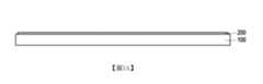
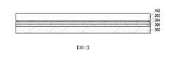
請參照圖1A,提供承載晶圓100。在一些實施例中,承載晶圓100可為半導體晶圓,如矽晶圓,但本發明並不以此為限。Referring to FIG. 1A , a
接著,在溫度T1下,在承載晶圓100上塗佈黏著劑層200。黏著劑層200在溫度T1下具有黏著強度S1,黏著劑層200在溫度T2下具有黏著強度S2,且黏著強度S1小於黏著強度S2。溫度T1為低於黏著劑層200的黏著強度轉換溫度ST1的溫度,且溫度T2為高於或等於黏著劑層200的黏著強度轉換溫度ST1的溫度。在低於黏著強度轉換溫度ST1的溫度下,黏著劑層200的黏著強度會大幅降低。此外,在高於或等於黏著強度轉換溫度ST1的溫度下,黏著劑層200的黏著強度會大幅增加。因此,黏著劑層200在溫度T1下可具有較小的黏著強度,且黏著劑層200在溫度T2下可具有較大的黏著強度。Next, the
在一些實施例中,黏著劑層200的黏著強度轉換溫度ST1可為-50℃至15℃。在一些實施例中,溫度T1可為高於或等於-100℃且低於15℃。在一些實施例中,溫度T2可為-50℃至500℃。在一些實施例中,在承載晶圓100上塗佈黏著劑層200的方法例如是旋轉塗佈法。In some embodiments, the adhesive strength transition temperature ST1 of the
在一些實施例中,在承載晶圓100上塗佈黏著劑層200之後,可對黏著劑層200進行邊緣球狀物移除(edge bead removal,EBR)製程,以移除位在承載晶圓100的邊緣的黏著劑層200。In some embodiments, after the
請參照圖1B,在溫度T2下,藉由黏著劑層200將元件晶圓300與承載晶圓100彼此接合。由於黏著劑層200在溫度T2下可具有較大的黏著強度,因此元件晶圓300與承載晶圓100可藉由黏著劑層200而穩固地接合在一起。在一些實施例中,元件晶圓300可為半導體晶圓,如矽晶圓。此外,在元件晶圓300上可具有所需的半導體元件(未示出)。在一些實施例中,位在元件晶圓300上的半導體元件可包括動態隨機存取記憶體(dynamic random access memory,DRAM)元件,但本發明並不以此為限。Referring to FIG. 1B , at temperature T2 , the component wafer 300 and the
請參照圖1C,在將元件晶圓300與承載晶圓100彼此接合之後,可在溫度T2下,對元件晶圓300進行加工製程。在溫度T2下進行的加工製程中,由於黏著劑層200在溫度T2下可具有較大的黏著強度,因此可有效地防止元件晶圓300及/或承載晶圓100因滑動或剝離而造成損壞。在一些實施例中,加工製程可包括晶圓薄化製程、重佈線層製程或其組合,但本發明並不以此為限。在本實施例中,可對元件晶圓300進行晶圓薄化製程,以降低元件晶圓300的厚度,但本發明並不以此為限。在另一些實施例中,可不對元件晶圓300進行晶圓薄化製程。Referring to FIG. 1C , after the
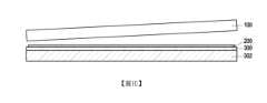
請參照圖1D,在溫度T2下,將元件晶圓302與元件晶圓300彼此接合。在溫度T2下,將元件晶圓302與元件晶圓300彼此接合的過程中,由於黏著劑層200在溫度T2下可具有較大的黏著強度,因此可有效地防止元件晶圓300及/或承載晶圓100因滑動或剝離而造成損壞。在一些實施例中,元件晶圓302與元件晶圓300可為相同或不同的元件晶圓。在一些實施例中,元件晶圓302可為半導體晶圓,如矽晶圓。此外,在元件晶圓302上可具有所需的半導體元件(未示出)。在一些實施例中,位在元件晶圓302上的半導體元件可包括動態隨機存取記憶體元件,但本發明並不以此為限。在一些實施例中,將元件晶圓302與元件晶圓300彼此接合的方法例如是混合接合法或熔融接合法。Referring to FIG. 1D, at temperature T2, the
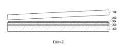
請參照圖1E,在溫度T1下,剝離承載晶圓100。藉此,可使承載晶圓100與元件晶圓300分離。由於黏著劑層200在溫度T1下可具有較小的黏著強度,因此可在溫度T1下輕易地將承載晶圓100剝離,且可有效地防止元件晶圓300在剝離過程中損壞。Referring to FIG. 1E, at temperature T1, the
在上述實施例中,不同製程中的溫度T1可為相同溫度或不同溫度。只要溫度T1為低於黏著劑層200的黏著強度轉換溫度ST1的溫度,即屬於本發明所涵蓋的範圍。在上述實施例中,不同製程中的溫度T2可為相同溫度或不同溫度。只要溫度T2為高於或等於黏著劑層200的黏著強度轉換溫度ST1的溫度,即屬於本發明所涵蓋的範圍。In the above embodiments, the temperatures T1 in different processes can be the same temperature or different temperatures. As long as the temperature T1 is lower than the adhesive strength transition temperature ST1 of the
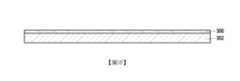
請參照圖1F,在剝離承載晶圓100之後,可移除位在元件晶圓300上的黏著劑層200。在一些實施例中,黏著劑層200的移除方法例如是溶劑移除法或灰化法。Referring to FIG. 1F , after peeling off the
請參照圖1G,可提供承載晶圓102。在一些實施例中,承載晶圓102可為半導體晶圓,如矽晶圓,但本發明並不以此為限。在一些實施例中,承載晶圓102與承載晶圓100可為同一個承載晶圓,亦即可將承載晶圓重複使用,但本發明並不以此為限。在另一些實施例中,承載晶圓102與承載晶圓100可為不同承載晶圓。Referring to Figure 1G, a
接著,可在溫度T3下,在承載晶圓102上塗佈黏著劑層202。黏著劑層202在溫度T3下可具有黏著強度S3,黏著劑層202在溫度T4下可具有黏著強度S4,且黏著強度S3可小於黏著強度S4。溫度T3可為低於黏著劑層202的黏著強度轉換溫度ST2的溫度,且溫度T4可為高於或等於黏著劑層202的黏著強度轉換溫度ST2的溫度。在低於黏著強度轉換溫度ST2的溫度下,黏著劑層202的黏著強度會大幅降低。此外,在高於或等於黏著強度轉換溫度ST2的溫度下,黏著劑層202的黏著強度會大幅增加。因此,黏著劑層202在溫度T3下可具有較小的黏著強度,且黏著劑層202在溫度T4下可具有較大的黏著強度。Then, the
在一些實施例中,黏著劑層202的黏著強度轉換溫度ST2可為-50℃至15℃。在一些實施例中,溫度T3可為高於或等於-100℃且低於15℃。在一些實施例中,溫度T4可為-50℃至500℃。在一些實施例中,在承載晶圓102上塗佈黏著劑層202的方法例如是旋轉塗佈法。In some embodiments, the adhesive strength transition temperature ST2 of the
在一些實施例中,黏著劑層202與黏著劑層200可為相同或不同的黏著劑層。在一些實施例中,黏著劑層202與黏著劑層200可具有相同或不同的黏著強度轉換溫度。亦即,黏著劑層202的黏著強度轉換溫度ST2與黏著劑層200的黏著強度轉換溫度ST1可為相同或不同。在一些實施例中,黏著劑層202與黏著劑層200可具有相同或不同的黏著強度。亦即,黏著劑層202在溫度T3下的黏著強度S3與黏著劑層200在溫度T1下的黏著強度S1可為相同或不同。此外,黏著劑層202在溫度T4下的黏著強度S4與黏著劑層200在溫度T2下的黏著強度S2可為相同或不同。In some embodiments, the
在一些實施例中,在承載晶圓102上塗佈黏著劑層202之後,可對黏著劑層202進行邊緣球狀物移除(EBR)製程,以移除位在承載晶圓102的邊緣的黏著劑層202。In some embodiments, after the
請參照圖1H,可在溫度T4下,藉由黏著劑層202將元件晶圓304與承載晶圓102彼此接合。由於黏著劑層202在溫度T4下可具有較大的黏著強度,因此元件晶圓304與承載晶圓102可藉由黏著劑層202而穩固地接合在一起。在一些實施例中,元件晶圓304、元件晶圓302與元件晶圓300可為相同或不同的元件晶圓。在一些實施例中,元件晶圓304可為半導體晶圓,如矽晶圓。此外,在元件晶圓304上可具有所需的半導體元件(未示出)。在一些實施例中,位在元件晶圓304上的半導體元件可包括動態隨機存取記憶體元件,但本發明並不以此為限。Referring to FIG. 1H , the
請參照圖1I,在將元件晶圓304與承載晶圓102彼此接合之後,可在溫度T4下,對元件晶圓304進行加工製程。在溫度T4下進行的加工製程中,由於黏著劑層202在溫度T4下可具有較大的黏著強度,因此可有效地防止元件晶圓304及/或承載晶圓102因滑動或剝離而造成損壞。在一些實施例中,加工製程可包括晶圓薄化製程、重佈線層製程或其組合,但本發明並不以此為限。在本實施例中,可對元件晶圓304進行晶圓薄化製程,以降低元件晶圓304的厚度,但本發明並不以此為限。在另一些實施例中,可不對元件晶圓304進行晶圓薄化製程。Referring to FIG. 1I , after the
請參照圖1J,可在溫度T4下,將元件晶圓300與元件晶圓304彼此接合。在溫度T4下,將元件晶圓300與元件晶圓304彼此接合的過程中,由於黏著劑層202在溫度T4下可具有較大的黏著強度,因此可有效地防止元件晶圓304及/或承載晶圓102因滑動或剝離而造成損壞。在一些實施例中,將元件晶圓300與元件晶圓304彼此接合的方法例如是混合接合法或熔融接合法。Referring to FIG. 1J , the
請參照圖1K,可在溫度T3下,剝離承載晶圓102。藉此,可使承載晶圓102與元件晶圓304分離。由於黏著劑層202在溫度T3下可具有較小的黏著強度,因此可在溫度T3下輕易地將承載晶圓102剝離,且可有效地防止元件晶圓304在剝離過程中損壞。Referring to FIG. 1K , the
在上述實施例中,不同製程中的溫度T3可為相同溫度或不同溫度。只要溫度T3可為低於黏著劑層202的黏著強度轉換溫度ST2的溫度,即屬於本發明所涵蓋的範圍。在上述實施例中,不同製程中的溫度T4可為相同溫度或不同溫度。只要溫度T4可為高於或等於黏著劑層202的黏著強度轉換溫度ST2的溫度,即屬於本發明所涵蓋的範圍。In the above embodiment, the temperature T3 in different processes can be the same temperature or different temperatures. As long as the temperature T3 can be a temperature lower than the adhesion strength transition temperature ST2 of the
請參照圖1L,在剝離承載晶圓102之後,可移除位在元件晶圓304上的黏著劑層202。在一些實施例中,黏著劑層202的移除方法例如是溶劑移除法或灰化法。Referring to FIG. 1L , after peeling off the
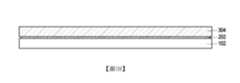
在本實施例中,是以將三個元件晶圓(如,元件晶圓300、元件晶圓302與元件晶圓304)進行接合為例,但本發明並不以此為限。只要是藉由上述方法將至少兩個元件晶圓進行接合,即屬於本發明所涵蓋的範圍。在一些實施例中,更可重複進行如圖1G至圖1L所示的製程,而將一個以上的其他元件晶圓(未示出)接合在元件晶圓304上。亦即,在一些實施例中,更可將四個以上的元件晶圓進行接合。In this embodiment, three component wafers (eg,
基於上述實施例可知,在晶圓接合方法中,黏著劑層200在低於黏著劑層200的黏著強度轉換溫度ST1的溫度T1下具有黏著強度S1,黏著劑層200在高於或等於黏著劑層200的黏著強度轉換溫度ST1的溫度T2下具有黏著強度S2,且黏著強度S1小於黏著強度S2。在低於黏著強度轉換溫度ST1的溫度下,黏著劑層200的黏著強度會大幅降低。此外,在高於或等於黏著強度轉換溫度ST1的溫度下,黏著劑層200的黏著強度會大幅增加。因此,黏著劑層200在溫度T1下可具有較小的黏著強度,且黏著劑層200在溫度T2下可具有較大的黏著強度。Based on the above embodiments, it can be seen that in the wafer bonding method, the
如此一來,在溫度T2下,將元件晶圓302與元件晶圓300彼此接合的過程中,由於黏著劑層200在溫度T2下可具有較大的黏著強度,因此可有效地防止元件晶圓300及/或承載晶圓100因滑動或剝離而造成損壞。此外,在對接合於承載晶圓100的元件晶圓300進行後續高溫製程(如,回火製程時及/或重佈線層製程)的過程中,由於上述高溫製程的製程溫度通常高於黏著劑層200的黏著強度轉換溫度ST1,因此黏著劑層200可具有較大的黏著強度,藉此可有效地防止元件晶圓300及/或承載晶圓100因滑動或剝離而造成損壞。In this way, during the process of bonding the
另外,由於承載晶圓100是在溫度T1下進行剝離,因此黏著劑層200可具有較小的黏著強度。如此一來,可在溫度T1下輕易地將承載晶圓100剝離,且可有效地防止元件晶圓300在剝離過程中損壞。In addition, since the
綜上所述,在上述實施例的晶圓接合方法中,黏著劑層在低於黏著劑層的黏著強度轉換溫度的第一溫度下具有第一黏著強度,黏著劑層在高於或等於黏著劑層的黏著強度轉換溫度的第二溫度下具有第二黏著強度,且第一黏著強度小於第二黏著強度。在低於黏著強度轉換溫度的溫度下,黏著劑層的黏著強度會大幅降低。此外,在高於或等於黏著強度轉換溫度的溫度下,黏著劑層的黏著強度會大幅增加。因此,黏著劑層在第一溫度下可具有較小的黏著強度,且黏著劑層在第二溫度下可具有較大的黏著強度。如此一來,在對接合於承載晶圓的元件晶圓進行後續製程的過程中及/或在剝離承載晶圓的過程中,可有效地防止元件晶圓及/或承載晶圓損壞。To sum up, in the wafer bonding method of the above embodiments, the adhesive layer has a first adhesive strength at a first temperature lower than the adhesive strength transition temperature of the adhesive layer, and the adhesive layer has a first adhesive strength at a temperature higher than or equal to the adhesive strength transition temperature of the adhesive layer. The adhesive strength of the agent layer has a second adhesive strength at the second temperature of the conversion temperature, and the first adhesive strength is smaller than the second adhesive strength. At temperatures below the adhesion strength transition temperature, the adhesion strength of the adhesive layer will be significantly reduced. In addition, at temperatures higher than or equal to the adhesion strength transition temperature, the adhesion strength of the adhesive layer will increase significantly. Therefore, the adhesive layer may have a smaller adhesive strength at the first temperature, and the adhesive layer may have a larger adhesive strength at the second temperature. In this way, damage to the component wafer and/or the carrier wafer can be effectively prevented during subsequent processes of the component wafer bonded to the carrier wafer and/or during the process of peeling off the carrier wafer.
雖然本發明已以實施例揭露如上,然其並非用以限定本發明,任何所屬技術領域中具有通常知識者,在不脫離本發明的精神和範圍內,當可作些許的更動與潤飾,故本發明的保護範圍當視後附的申請專利範圍所界定者為準。Although the present invention has been disclosed above through embodiments, they are not intended to limit the present invention. Anyone with ordinary knowledge in the technical field may make some modifications and modifications without departing from the spirit and scope of the present invention. Therefore, The protection scope of the present invention shall be determined by the appended patent application scope.
100, 102:承載晶圓100, 102: Carrier wafer
200, 202:黏著劑層200, 202: Adhesive layer
300, 302, 304:元件晶圓300, 302, 304: component wafer
圖1A至圖1L為根據本發明的一些實施例的晶圓接合流程的剖面圖。1A-1L are cross-sectional views of a wafer bonding process according to some embodiments of the present invention.
100:承載晶圓100: Carrying wafer
200:黏著劑層200: Adhesive layer
300,302:元件晶圓300,302: component wafer
Claims (8)
Translated fromChinesePriority Applications (1)
| Application Number | Priority Date | Filing Date | Title |
|---|---|---|---|
| TW111144128ATWI818806B (en) | 2022-11-18 | 2022-11-18 | Wafer bonding method |
Applications Claiming Priority (1)
| Application Number | Priority Date | Filing Date | Title |
|---|---|---|---|
| TW111144128ATWI818806B (en) | 2022-11-18 | 2022-11-18 | Wafer bonding method |
Publications (2)
| Publication Number | Publication Date |
|---|---|
| TWI818806Btrue TWI818806B (en) | 2023-10-11 |
| TW202422637A TW202422637A (en) | 2024-06-01 |
Family
ID=89857637
Family Applications (1)
| Application Number | Title | Priority Date | Filing Date |
|---|---|---|---|
| TW111144128ATWI818806B (en) | 2022-11-18 | 2022-11-18 | Wafer bonding method |
Country Status (1)
| Country | Link |
|---|---|
| TW (1) | TWI818806B (en) |
Citations (4)
| Publication number | Priority date | Publication date | Assignee | Title |
|---|---|---|---|---|
| TWI397131B (en)* | 2005-03-01 | 2013-05-21 | Dow Corning | Temporary wafer bonding method for semiconductor processing |
| TW201619315A (en)* | 2014-11-07 | 2016-06-01 | 萬國商業機器公司 | Adhesive resins for wafer bonding |
| TW201724173A (en)* | 2015-06-02 | 2017-07-01 | 信越化學工業股份有限公司 | Method for producing composite wafer provided with oxide single-crystal thin film |
| TW202115149A (en)* | 2019-09-30 | 2021-04-16 | 日商日立化成股份有限公司 | Adhesive for semiconductors, adhesive sheet for semiconductors, and method for manufacturing semiconductor device |
- 2022
- 2022-11-18TWTW111144128Apatent/TWI818806B/enactive
Patent Citations (4)
| Publication number | Priority date | Publication date | Assignee | Title |
|---|---|---|---|---|
| TWI397131B (en)* | 2005-03-01 | 2013-05-21 | Dow Corning | Temporary wafer bonding method for semiconductor processing |
| TW201619315A (en)* | 2014-11-07 | 2016-06-01 | 萬國商業機器公司 | Adhesive resins for wafer bonding |
| TW201724173A (en)* | 2015-06-02 | 2017-07-01 | 信越化學工業股份有限公司 | Method for producing composite wafer provided with oxide single-crystal thin film |
| TW202115149A (en)* | 2019-09-30 | 2021-04-16 | 日商日立化成股份有限公司 | Adhesive for semiconductors, adhesive sheet for semiconductors, and method for manufacturing semiconductor device |
Also Published As
| Publication number | Publication date |
|---|---|
| TW202422637A (en) | 2024-06-01 |
Similar Documents
| Publication | Publication Date | Title |
|---|---|---|
| US8846499B2 (en) | Composite carrier structure | |
| US9679867B2 (en) | Semiconductor device having a low-adhesive bond substrate pair | |
| JP7173000B2 (en) | Semiconductor device manufacturing method and expanded tape | |
| US8697542B2 (en) | Method for thin die-to-wafer bonding | |
| JP5970071B2 (en) | Device structure manufacturing method and structure | |
| US10049909B2 (en) | Wafer handler and methods of manufacture | |
| US9281182B2 (en) | Pre-cut wafer applied underfill film | |
| JP2011071487A (en) | Layer bonding and process for transferring layer | |
| CN114188263A (en) | A method of sealing wafer using carrier disc | |
| TWI818806B (en) | Wafer bonding method | |
| CN102486992A (en) | A method of manufacturing a semiconductor device | |
| CN112201574B (en) | Multi-layer wafer bonding method | |
| JP7551787B2 (en) | Wafer back grinding method and electronic device manufacturing method | |
| CN114628240B (en) | Method for stacking chip wafers | |
| US9013039B2 (en) | Wafer support system for 3D packaging | |
| US10163673B2 (en) | Dual adhesive bonding with perforated wafer | |
| JP2013069946A (en) | Support substrate, manufacturing method of support substrate, and manufacturing method of semiconductor device | |
| Sakamoto et al. | A Temporary Bonding De-Bonding Tape with High Thermal Resistance and Excellent TTV for 3DIC | |
| CN109196627B (en) | Method for manufacturing semiconductor structure comprising interposer without any through hole | |
| Phommahaxay et al. | Demonstration of a novel low cost single material temporary bond solution for high topography substrates based on a mechanical wafer debonding and innovative adhesive removal | |
| JPH05109679A (en) | Manufacture of semiconductor device | |
| US20250293074A1 (en) | Method for producing semiconductor device, and expandable tape | |
| US20250183088A1 (en) | Method for removing residues from a substrate surface | |
| Nakano et al. | A Temporary Bonding De-Bonding Tape with High Thermal Resistance, Easy peeling and Excellent TTV for 3DIC | |
| JPS5952840A (en) | Manufacture of semiconductor device |