TWI814151B - Display apparatus - Google Patents
Display apparatusDownload PDFInfo
- Publication number
- TWI814151B TWI814151BTW110144075ATW110144075ATWI814151BTW I814151 BTWI814151 BTW I814151BTW 110144075 ATW110144075 ATW 110144075ATW 110144075 ATW110144075 ATW 110144075ATW I814151 BTWI814151 BTW I814151B
- Authority
- TW
- Taiwan
- Prior art keywords
- light
- emitting element
- distance
- conductive pattern
- conductive
- Prior art date
Links
Images


Classifications
- H—ELECTRICITY
- H01—ELECTRIC ELEMENTS
- H01L—SEMICONDUCTOR DEVICES NOT COVERED BY CLASS H10
- H01L25/00—Assemblies consisting of a plurality of semiconductor or other solid state devices
- H01L25/03—Assemblies consisting of a plurality of semiconductor or other solid state devices all the devices being of a type provided for in a single subclass of subclasses H10B, H10D, H10F, H10H, H10K or H10N, e.g. assemblies of rectifier diodes
- H01L25/04—Assemblies consisting of a plurality of semiconductor or other solid state devices all the devices being of a type provided for in a single subclass of subclasses H10B, H10D, H10F, H10H, H10K or H10N, e.g. assemblies of rectifier diodes the devices not having separate containers
- H01L25/075—Assemblies consisting of a plurality of semiconductor or other solid state devices all the devices being of a type provided for in a single subclass of subclasses H10B, H10D, H10F, H10H, H10K or H10N, e.g. assemblies of rectifier diodes the devices not having separate containers the devices being of a type provided for in group H10H20/00
- H01L25/0753—Assemblies consisting of a plurality of semiconductor or other solid state devices all the devices being of a type provided for in a single subclass of subclasses H10B, H10D, H10F, H10H, H10K or H10N, e.g. assemblies of rectifier diodes the devices not having separate containers the devices being of a type provided for in group H10H20/00 the devices being arranged next to each other
- H—ELECTRICITY
- H10—SEMICONDUCTOR DEVICES; ELECTRIC SOLID-STATE DEVICES NOT OTHERWISE PROVIDED FOR
- H10H—INORGANIC LIGHT-EMITTING SEMICONDUCTOR DEVICES HAVING POTENTIAL BARRIERS
- H10H29/00—Integrated devices, or assemblies of multiple devices, comprising at least one light-emitting semiconductor element covered by group H10H20/00
- H10H29/10—Integrated devices comprising at least one light-emitting semiconductor component covered by group H10H20/00
- H10H29/14—Integrated devices comprising at least one light-emitting semiconductor component covered by group H10H20/00 comprising multiple light-emitting semiconductor components
- H10H29/142—Two-dimensional arrangements, e.g. asymmetric LED layout
- H—ELECTRICITY
- H10—SEMICONDUCTOR DEVICES; ELECTRIC SOLID-STATE DEVICES NOT OTHERWISE PROVIDED FOR
- H10H—INORGANIC LIGHT-EMITTING SEMICONDUCTOR DEVICES HAVING POTENTIAL BARRIERS
- H10H20/00—Individual inorganic light-emitting semiconductor devices having potential barriers, e.g. light-emitting diodes [LED]
- H10H20/80—Constructional details
- H10H20/83—Electrodes
- H10H20/831—Electrodes characterised by their shape
- H10H20/8312—Electrodes characterised by their shape extending at least partially through the bodies
- H—ELECTRICITY
- H10—SEMICONDUCTOR DEVICES; ELECTRIC SOLID-STATE DEVICES NOT OTHERWISE PROVIDED FOR
- H10H—INORGANIC LIGHT-EMITTING SEMICONDUCTOR DEVICES HAVING POTENTIAL BARRIERS
- H10H20/00—Individual inorganic light-emitting semiconductor devices having potential barriers, e.g. light-emitting diodes [LED]
- H10H20/80—Constructional details
- H10H20/85—Packages
- H10H20/851—Wavelength conversion means
- H10H20/8514—Wavelength conversion means characterised by their shape, e.g. plate or foil
- H—ELECTRICITY
- H10—SEMICONDUCTOR DEVICES; ELECTRIC SOLID-STATE DEVICES NOT OTHERWISE PROVIDED FOR
- H10H—INORGANIC LIGHT-EMITTING SEMICONDUCTOR DEVICES HAVING POTENTIAL BARRIERS
- H10H20/00—Individual inorganic light-emitting semiconductor devices having potential barriers, e.g. light-emitting diodes [LED]
- H10H20/80—Constructional details
- H10H20/85—Packages
- H10H20/857—Interconnections, e.g. lead-frames, bond wires or solder balls
Landscapes
- Engineering & Computer Science (AREA)
- Power Engineering (AREA)
- Microelectronics & Electronic Packaging (AREA)
- Physics & Mathematics (AREA)
- Condensed Matter Physics & Semiconductors (AREA)
- General Physics & Mathematics (AREA)
- Computer Hardware Design (AREA)
- Devices For Indicating Variable Information By Combining Individual Elements (AREA)
- Control Of Indicators Other Than Cathode Ray Tubes (AREA)
- Preparation Of Compounds By Using Micro-Organisms (AREA)
- Measuring Pulse, Heart Rate, Blood Pressure Or Blood Flow (AREA)
- Compounds Of Unknown Constitution (AREA)
Abstract
Description
Translated fromChinese本發明是有關於一種光電裝置,且特別是有關於一種顯示裝置。The present invention relates to an optoelectronic device, and in particular to a display device.
隨著顯示技術的演進,具有高解析與薄型化的顯示裝置受到主流市場的喜愛。近幾年來,由於發光二極體(Light-Emitting Diode;LED)元件的製程技術的突破,已發展出可將發光二極體元件以陣列排列製作出的微型發光二極體顯示裝置(Micro-LED display)或毫米等級的發光二極體顯示裝置等,其不需要設置液晶層(Liquid crystal)及彩色濾光片(Color filter),而能進一步減少顯示裝置的厚度。此外,相較於有機發光二極體顯示裝置,微型發光二極體顯示裝置具有更省電、壽命更長的優勢。With the evolution of display technology, display devices with high resolution and thinness are favored by the mainstream market. In recent years, due to breakthroughs in the process technology of light-emitting diode (LED) components, micro-light-emitting diode display devices (Micro-LEDs) that can be produced by arranging light-emitting diode components in an array have been developed. LED display) or millimeter-level light-emitting diode display devices, etc., which do not require a liquid crystal layer (Liquid crystal) and color filter (Color filter), and can further reduce the thickness of the display device. In addition, compared with organic light-emitting diode display devices, micro-light-emitting diode display devices have the advantages of more power saving and longer life.
在目前微型發光二極體顯示裝置的製作過程中,需透過巨量轉移(Mass transfer)將大量的發光二極體元件轉置於驅動背板上。被轉置於驅動背板的發光二極體元件可能有少部分異常,異常的發光二極體元件需被移除。然後,再將修補用的發光二極體元件轉置於驅動背板上,以完成修補動作。然而,在進行修補動作時,拾取修補用之發光二極體元件的轉置元件卻會壓傷原本已轉置於驅動背板上且正常的發光二極體元件,影響微型發光二極體顯示裝置的良率。In the current manufacturing process of micro-LED display devices, a large number of LED elements need to be transferred to the driving backplane through mass transfer. There may be a small number of abnormalities in the light-emitting diode components that are transferred to the driving backplane, and the abnormal light-emitting diode components need to be removed. Then, the light-emitting diode component for repair is transferred to the driving backplane to complete the repair operation. However, during the repair operation, picking up the transposed components of the LED components used for repair will crush the normal LED components that have been relocated to the driving backplane, affecting the micro LED display. Device yield.
本發明提供一種顯示裝置,易修補。The invention provides a display device which is easy to repair.
本發明提供另一種顯示裝置,也易修補。The present invention provides another display device that is also easy to repair.
本發明一實施例的顯示裝置包括驅動背板及多個發光元件。驅動背板包括基底、設置於基底上的多個畫素驅動電路及導電層。導電層具有多個導電圖案,其中多個導電圖案分別電性連接至多個畫素驅動電路。多個發光元件分別電性連接至多個導電圖案,其中每一發光元件具有背向基底的頂面。多個發光元件包括第一發光元件及第二發光元件。多個導電圖案包括第一導電圖案及第二導電圖案。第一發光元件及第二發光元件分別電性連接至第一導電圖案及第二導電圖案。第一發光元件的頂面與第一導電圖案具有第一距離。第二發光元件的頂面與第二導電圖案具有第二距離,且第二距離大於第一距離。A display device according to an embodiment of the present invention includes a driving backplane and a plurality of light-emitting elements. The driving backplane includes a substrate, a plurality of pixel driving circuits and a conductive layer disposed on the substrate. The conductive layer has a plurality of conductive patterns, wherein the plurality of conductive patterns are electrically connected to a plurality of pixel driving circuits respectively. A plurality of light-emitting elements are electrically connected to a plurality of conductive patterns respectively, wherein each light-emitting element has a top surface facing away from the substrate. The plurality of light-emitting elements include a first light-emitting element and a second light-emitting element. The plurality of conductive patterns include first conductive patterns and second conductive patterns. The first light-emitting element and the second light-emitting element are electrically connected to the first conductive pattern and the second conductive pattern respectively. The top surface of the first light emitting element has a first distance from the first conductive pattern. The top surface of the second light-emitting element has a second distance from the second conductive pattern, and the second distance is greater than the first distance.
本發明另一實施例的顯示裝置包括驅動背板及多個發光元件。驅動背板包括基底、設置於基底上的多個畫素驅動電路及接墊層。接墊層具有多個接墊組,其中多個接墊組分別電性連接至多個畫素驅動電路。多個發光元件分別電性連接至多個接墊組。多個發光元件包括第一發光元件及第二發光元件。多個接墊組包括第一接墊組及第二接墊組。第一發光元件及第二發光元件分別電性連接至第一接墊組及第二接墊組。第二接墊組的至少一接墊與基底的距離大於第一接墊組的至少一接墊與基底的距離。A display device according to another embodiment of the present invention includes a driving backplane and a plurality of light-emitting elements. The driving backplane includes a substrate, a plurality of pixel driving circuits disposed on the substrate, and a pad layer. The pad layer has a plurality of pad groups, wherein the plurality of pad groups are electrically connected to a plurality of pixel driving circuits respectively. The plurality of light-emitting elements are electrically connected to the plurality of pad groups respectively. The plurality of light-emitting elements include a first light-emitting element and a second light-emitting element. The plurality of pad groups include a first pad group and a second pad group. The first light-emitting element and the second light-emitting element are electrically connected to the first pad group and the second pad group respectively. The distance between at least one pad of the second pad group and the substrate is greater than the distance between at least one pad of the first pad group and the substrate.
現將詳細地參考本發明的示範性實施例,示範性實施例的實例說明於附圖中。只要有可能,相同元件符號在圖式和描述中用來表示相同或相似部分。Reference will now be made in detail to the exemplary embodiments of the present invention, examples of which are illustrated in the accompanying drawings. Whenever possible, the same reference numbers are used in the drawings and descriptions to refer to the same or similar parts.
應當理解,當諸如層、膜、區域或基板的元件被稱為在另一元件“上”或“連接到”另一元件時,其可以直接在另一元件上或與另一元件連接,或者中間元件可以也存在。相反,當元件被稱為“直接在另一元件上”或“直接連接到”另一元件時,不存在中間元件。如本文所使用的,“連接”可以指物理及/或電性連接。再者,“電性連接”或“耦合”可以是二元件間存在其它元件。It will be understood that when an element such as a layer, film, region or substrate is referred to as being "on" or "connected to" another element, it can be directly on or connected to the other element, or Intermediate elements may also be present. In contrast, when an element is referred to as being "directly on" or "directly connected to" another element, there are no intervening elements present. As used herein, "connected" may refer to a physical and/or electrical connection. Furthermore, "electrical connection" or "coupling" may mean the presence of other components between two components.
除非另有定義,本文使用的所有術語(包括技術和科學術語)具有與本發明所屬領域的普通技術人員通常理解的相同的含義。將進一步理解的是,諸如在通常使用的字典中定義的那些術語應當被解釋為具有與它們在相關技術和本發明的上下文中的含義一致的含義,並且將不被解釋為理想化的或過度正式的意義,除非本文中明確地這樣定義。Unless otherwise defined, all terms (including technical and scientific terms) used herein have the same meaning as commonly understood by one of ordinary skill in the art to which this invention belongs. It will be further understood that terms such as those defined in commonly used dictionaries should be construed to have meanings consistent with their meanings in the context of the relevant technology and the present invention, and are not to be construed as idealistic or excessive Formal meaning, unless expressly defined as such herein.
圖1A至圖1C示出本發明一實施例之顯示裝置的修補過程。1A to 1C illustrate a repair process of a display device according to an embodiment of the present invention.
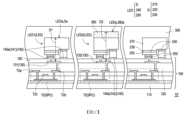
請參照圖1A,顯示裝置10包括驅動背板100。驅動背板100包括基底110。舉例而言,在本實施例中,基底110的材質可以是玻璃、石英、有機聚合物、或是其它可適用的材料。Referring to FIG. 1A , the
顯示裝置10還包括多個畫素驅動電路SPC,設置於基底110上的。舉例而言,在本實施例中,每一畫素驅動電路SPC可包括資料線(未繪示)、掃描線(未繪示)、電源線(未繪示)、共通線(未繪示)、第一電晶體(未繪示)、第二電晶體T2及電容(未繪示),其中第一電晶體的第一端電性連接至資料線,第一電晶體的控制端電性連接至掃描線,第一電晶體的第二端電性連接至第二電晶體T2的控制端T2c,第二電晶體T2的第一端T2a電性連接至電源線,且電容電性連接至第一電晶體的第二端及第二電晶體T2的第一端T2a;但本發明不以此為限。The
驅動背板100還包括導電層130,具有多個導電圖案131、132,其中多個導電圖案131、132分別電性連接至多個畫素驅動電路SPC。舉例而言,在本實施例中,多個導電圖案131、132的每一者可電性連接至對應一畫素驅動電路SPC的第二電晶體T2的第二端T2b,但本發明不以此為限。The
在本實施例中,導電層130例如是透明導電層,其包括金屬氧化物,例如:銦錫氧化物、銦鋅氧化物、鋁錫氧化物、鋁鋅氧化物、銦鍺鋅氧化物、其它合適的氧化物、或者是上述至少二者的堆疊層,但本發明不以此為限。In this embodiment, the
驅動背板100還包括接墊層140,具有多個接墊組141、142。多個接墊組141、142分別電性連接至多個畫素驅動電路SPC。每一接墊組141、142包括多個接墊140a,每一接墊組141、142的一個接墊140a電性連接至多個導電圖案131、132之中對應的一個,每一接墊組141、142的另一接墊140a電性連接至對應的一畫素驅動電路SPC的共通線(未繪示)。The
在本實施例中,導電層130可設置於多個畫素驅動電路SPC上;驅動背板100還可包括介電層120,設置於導電層130與多個畫素驅動電路SPC之間。在本實施例中,接墊層140設置於導電層130上,驅動背板100還可包括另一介電層150,設置於接墊層140與導電層130之間。在本實施例中,介電層120、150的材料可為無機材料(例如:氧化矽、氮化矽、氮氧化矽、或上述至少二種材料的堆疊層)、有機材料或上述的組合。In this embodiment, the
顯示裝置10還包括多個發光元件LED,其中每一發光元件LED具有背向基底110的頂面LEDa。在本實施例中,每一發光元件LED包括晶粒D、多個電極240及多個導電凸塊250,晶粒D包括第一型半導體層210、第二型半導體層220及設置於第一型半導體層210與第二型半導體層220之間的主動層230,多個電極240分別電性連接至第一型半導體層210及第二型半導體層220,且多個導電凸塊250分別電性連接至多個電極240。每一發光元件LED的多個導電凸塊250分別電性連接至對應的一個接墊組141或142的多個接墊140a。The
多個發光元件LED分別電性連接至多個導電圖案131、132。詳細而言,在本實施例中,多個發光元件LED分別電性連接至多個接墊組141、142,且多個接墊組141、142分別電性連接至多個導電圖案131、132。在本實施例中,發光元件LED可包括微型發光二極體(μLED),但本發明不以此為限。The plurality of light emitting elements LED are electrically connected to the plurality of
請參照圖1A及圖1B,在本實施例中,可對顯示裝置10進行檢測,以檢測已轉置於驅動背板100上的發光元件LED是否正常。正常的發光元件LED(即第一發光元件LED1)會被保留在驅動背板100上,而異常的發光元件(未繪示)則會被移除。之後,再將修補用的發光元件LED(即第二發光元件LED2)轉置到驅動背板100且令修補用的發光元件LED與驅動背板100電性連接。Please refer to FIG. 1A and FIG. 1B . In this embodiment, the
值得注意的是,在本實施例中,相較於被保留在驅動背板100之正常的發光元件LED(即第一發光元件LED1),修補用的發光元件LED(即第二發光元件LED2)還包括色轉換圖案260,其中第二發光元件LED2的色轉換圖案260設置於第二發光元件LED2的晶粒D上。It is worth noting that in this embodiment, compared with the normal light-emitting element LED (that is, the first light-emitting element LED1) that is retained in the driving
利用轉置元件1將修補用的第二發光元件LED2轉置到驅動背板100上時,由於第二發光元件LED2本身具有色轉換圖案260,因此,當轉置元件1下壓,以使第二發光元件LED2與驅動背板100連接時,轉置元件1不易壓傷被保留在驅動背板100上之正常的第一發光元件LED1。When the transposition element 1 is used to transpose the second light-emitting element LED2 for repair onto the driving
請參照圖1B及圖1C,在完成上述修補動作後,可在驅動背板100上形成封裝層300,以覆蓋第一發光元件LED1及第二發光元件LED2,並完成修補後的顯示裝置10’。顯示裝置10’的多個發光元件LED包括第一發光元件LED1及第二發光元件LED2。顯示裝置10’的驅動背板100的多個導電圖案131、132包括第一導電圖案131及第二導電圖案132,第一發光元件LED1及第二發光元件LED2分別電性連接至第一導電圖案131及第二導電圖案132,第一發光元件LED1的頂面LEDa與第一導電圖案131具有第一距離D1,第二發光元件LED2的頂面LEDa與第二導電圖案132具有第二距離D2,且第二距離D2大於第一距離D1。Please refer to FIG. 1B and FIG. 1C. After the above repair operation is completed, an
在本實施例中,第一發光元件LED1的晶粒D具有第一發光元件LED1的頂面LEDa,第一發光元件LED1的晶粒D的頂面Da與第一導電圖案131具有第一距離D1,第二發光元件LED2包括晶粒D及色轉換圖案260,第二發光元件LED2的色轉換圖案260設置於第二發光元件LED2的晶粒D上,第二發光元件LED2的色轉換圖案260具有第二發光元件LED2的頂面LEDa,且第二發光元件LED2的色轉換圖案260的頂面260a與第二導電圖案132具有第二距離D2。也就是說,在本實施例中,第二發光元件LED2的色轉換圖案260的頂面260a與第二導電圖案132的距離(即第二距離D2)大於第一發光元件LED1的晶粒D的頂面Da與第一導電圖案131的距離(即第一距離D1),其中第一發光元件LED1的頂面LEDa及第二發光元件LED2的色轉換圖案260的頂面260a直接接觸於封裝層300。In this embodiment, the die D of the first light-emitting element LED1 has a top surface LEDa of the first light-emitting element LED1, and the top surface Da of the die D of the first light-emitting element LED1 has a first distance D1 from the first
在此必須說明的是,下述實施例沿用前述實施例的元件標號與部分內容,其中採用相同的標號來表示相同或近似的元件,並且省略了相同技術內容的說明。關於省略部分的說明可參考前述實施例,下述實施例不再重述。It must be noted here that the following embodiments follow the component numbers and part of the content of the previous embodiments, where the same numbers are used to represent the same or similar elements, and descriptions of the same technical content are omitted. For descriptions of omitted parts, reference may be made to the foregoing embodiments and will not be repeated in the following embodiments.
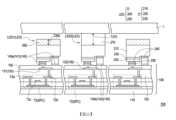
圖2A至圖2C示出本發明一實施例之顯示裝置的修補過程。2A to 2C illustrate a repair process of a display device according to an embodiment of the present invention.
圖2A至圖2C的顯示裝置10A、10A’與圖1A至圖1C的顯示裝置10、10’類似,兩者的差異在於:圖2A至圖2C的發光元件LED與圖1A至圖1C的發光元件LED不同。The
請參照圖2A,具體而言,在本實施例中,正常而被保留在驅動背板100上的第一發光元件LED包括晶粒D及色轉換圖案260,其中第一發光元件LED1的色轉換圖案260設置於第一發光元件LED1的晶粒D上;修補用的第二發光元件LED2包括晶粒D及透光圖案270,其中第二發光元件LED2的透光圖案270設置於第二發光元件LED2的晶粒D上。Please refer to FIG. 2A. Specifically, in this embodiment, the first light-emitting element LED that is normally retained on the driving
值得注意的是,第二發光元件LED2的透光圖案270的厚度T270大於第一發光元件LED1的色轉換圖案260的厚度T260。請參照圖2A及圖2B,藉此,利用轉置元件1將修補用的第二發光元件LED2轉置到驅動背板100上時,由於第二發光元件LED2的透光圖案270較厚,因此,當轉置元件1下壓,以使第二發光元件LED2與驅動背板100連接時,轉置元件1不易壓傷被保留在驅動背板100上之正常的第一發光元件LED1。It is worth noting that the thickness T270 of the light-transmitting
請參照圖2C,修補後的顯示裝置10A’的多個發光元件LED包括第一發光元件LED1及第二發光元件LED2。顯示裝置10A’的驅動背板100的多個導電圖案131、132包括第一導電圖案131及第二導電圖案132,第一發光元件LED1及第二發光元件LED2分別電性連接至第一導電圖案131及第二導電圖案132,第一發光元件LED1的頂面LEDa與第一導電圖案131具有第一距離D1,第二發光元件LED2的頂面LEDa與第二導電圖案132具有第二距離D2,且第二距離D2大於第一距離D1。Referring to FIG. 2C , the plurality of light-emitting elements LED of the repaired
在本實施例中,第二發光元件LED2的透光圖案270具有第二發光元件LED的頂面LEDa,第一發光元件LED1的色轉換圖案260具有第一發光元件LED1的頂面LEDa,第一發光元件LED1的色轉換圖案260的頂面260a與第一導電圖案131具有第一距離D1,且第二發光元件LED2的透光圖案270的頂面270a與第二導電圖案132具有第二距離D2。也就是說,在本實施例中,第二發光元件LED2的透光圖案270的頂面270a與第二導電圖案132的距離(即第二距離D2)大於第一發光元件LED1的色轉換圖案260的頂面260a與第一導電圖案131的距離(即第一距離D1),其中第一發光元件LED1的色轉換圖案260的頂面260a及第二發光元件LED2的透光圖案270的頂面260a直接接觸於封裝層300。In this embodiment, the light-transmitting
舉例而言,在本實施例中,第一發光元件LED1的晶粒D及第二發光元件LED2的晶粒D均是用以發出相同之第一色光(例如:藍光),第一發光元件LED1的色轉換圖案260用以將第一色光(例如:藍光)轉換為第二色光(例如:紅光或綠光),第二發光元件LED2的透光圖案270使第一色光(例如:藍光)通過而不轉換第一色光的顏色,但本發明不以此為限。For example, in this embodiment, the die D of the first light-emitting element LED1 and the die D of the second light-emitting element LED2 are both used to emit the same first color light (for example, blue light). The first light-emitting element The
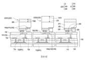
圖3A至圖3C示出本發明一實施例之顯示裝置的修補過程。3A to 3C illustrate a repair process of a display device according to an embodiment of the invention.
圖3A至圖3C的顯示裝置10B、10B’與圖1A至圖1C的顯示裝置10、10’類似,兩者的差異在於:圖3A至圖3C的多個發光元件LED與圖1A至圖1C的多個發光元件LED不同。The
請參照圖3A,具體而言,在本實施例中,正常而被保留在驅動背板100上的第一發光元件LED包括晶粒D及色轉換圖案260,其中第一發光元件LED1的色轉換圖案260設置於第一發光元件LED1的晶粒D上;修補用的第二發光元件LED2也包括晶粒D及色轉換圖案260,其中第二發光元件LED2的色轉換圖案260設置於第二發光元件LED2的晶粒D上。Please refer to FIG. 3A. Specifically, in this embodiment, the first light-emitting element LED that is normally retained on the driving
值得注意的是,修補用的第二發光元件LED2的色轉換圖案260的厚度T260-2大於第一發光元件LED1的色轉換圖案260的厚度T260-1。請參照圖3A及圖3B,藉此,利用轉置元件1將修補用的第二發光元件LED2轉置到驅動背板100上時,由於第二發光元件LED2的色轉換圖案260較厚,因此,轉置元件1下壓,以使第二發光元件LED2與驅動背板100連接時,轉置元件1不易壓傷被保留在驅動背板100上之正常的第一發光元件LED1。It is worth noting that the thickness T260-2 of the
請參照圖3C,修補後的顯示裝置10B’的多個發光元件LED包括第一發光元件LED1及第二發光元件LED2。顯示裝置10’的驅動背板100的多個導電圖案131、132包括第一導電圖案131及第二導電圖案132,第一發光元件LED1及第二發光元件LED2分別電性連接至第一導電圖案131及第二導電圖案132,第一發光元件LED1的頂面LEDa與第一導電圖案131具有第一距離D1,第二發光元件LED2的頂面LEDa與第二導電圖案132具有第二距離D2,且第二距離D2大於第一距離D1。Referring to FIG. 3C , the plurality of light-emitting elements LED of the repaired
在本實施例中,第二發光元件LED2的色轉換圖案260具有第二發光元件LED的頂面LEDa,第一發光元件LED1的色轉換圖案260具有第一發光元件LED1的頂面LEDa,第一發光元件LED1的色轉換圖案260的頂面260a與第一導電圖案131具有第一距離D1,且第二發光元件LED2的色轉換圖案260的頂面260a與第二導電圖案132具有第二距離D2。也就是說,在本實施例中,第二發光元件LED2的色轉換圖案260的頂面260a與第二導電圖案132的距離(即第二距離D2)大於第一發光元件LED1的晶粒D的色轉換圖案260的頂面260a與第一導電圖案131的距離(即第一距離D1),其中第一發光元件LED1的色轉換圖案260的頂面260a及第二發光元件LED2的色轉換圖案260的頂面260a直接接觸於封裝層300。In this embodiment, the
舉例而言,在本實施例中,第一發光元件LED1的晶粒D及第二發光元件LED2的晶粒D均是用以發出相同之第一色光(例如:藍光),第一發光元件LED1的色轉換圖案260用以將第一色光(例如:藍光)轉換為第二色光(例如:紅光),第二發光元件LED2的色轉換圖案260用以將第一色光(例如:藍光)轉換為第三色光(例如:綠光),但本發明不以此為限。For example, in this embodiment, the die D of the first light-emitting element LED1 and the die D of the second light-emitting element LED2 are both used to emit the same first color light (for example, blue light). The first light-emitting element The
圖4A至圖4C示出本發明一實施例之顯示裝置的修補過程。4A to 4C illustrate a repair process of a display device according to an embodiment of the present invention.
圖4A至圖4C的顯示裝置10C、10C’與圖1A至圖1C的顯示裝置10、10’類似,兩者的差異在於:圖4A至圖4C的多個發光元件LED與圖1A至圖1C的多個發光元件LED不同。The
請參照圖4A,具體而言,在本實施例中,第二發光元件LED2的多個導電凸塊250的至少一者的厚度T250-2大於第一發光元件LED1的多個導電凸塊250的至少一者的厚度T250-1。請參照圖4A及圖4B,藉此,利用轉置元件1將修補用的第二發光元件LED2轉置到驅動背板100上時,由於第二發光元件LED2的導電凸塊250較厚,因此,當轉置元件1下壓,以使第二發光元件LED2與驅動背板100連接時,轉置元件1不易壓傷被保留在驅動背板100上之正常的第一發光元件LED1。Please refer to FIG. 4A. Specifically, in this embodiment, the thickness T250-2 of at least one of the plurality of
請參照圖4C,修補後的顯示裝置10C’的多個發光元件LED包括第一發光元件LED1及第二發光元件LED2。顯示裝置10C’的驅動背板100的多個導電圖案131、132包括第一導電圖案131及第二導電圖案132,第一發光元件LED1及第二發光元件LED2分別電性連接至第一導電圖案131及第二導電圖案132,第一發光元件LED1的頂面LEDa與第一導電圖案131具有第一距離D1,第二發光元件LED2的頂面LEDa與第二導電圖案132具有第二距離D2,且第二距離D2大於第一距離D1。Referring to FIG. 4C , the plurality of light-emitting elements LED of the repaired
在本實施例中,第二發光元件LED2的晶粒D具有第二發光元件LED的頂面LEDa,第一發光元件LED1的晶粒D具有第一發光元件LED1的頂面LEDa,第一發光元件LED1的晶粒D的頂面Da與第一導電圖案131具有第一距離D1,且第二發光元件LED2的晶粒D的頂面Da與第二導電圖案132具有第二距離D2。也就是說,在本實施例中,第二發光元件LED2的晶粒D的頂面Da與第二導電圖案132的距離(即第二距離D2)大於第一發光元件LED1的晶粒D的頂面Da與第一導電圖案131的距離(即第一距離D1),其中第一發光元件LED1的晶粒D的頂面Da及第二發光元件LED2的晶粒D的頂面Da直接接觸於封裝層300。In this embodiment, the die D of the second light-emitting element LED2 has the top surface LEDa of the second light-emitting element LED, and the die D of the first light-emitting element LED1 has the top surface LEDa of the first light-emitting element LED1. There is a first distance D1 between the top surface Da of the die D of the LED1 and the first
圖5A至圖5C示出本發明一實施例之顯示裝置的修補過程。5A to 5C illustrate a repair process of a display device according to an embodiment of the present invention.
圖5A至圖5C的顯示裝置10D、10D’與圖1A至圖1C的顯示裝置10、10’類似,兩者的差異在於:圖5A至圖5C的多個發光元件LED與圖1A至圖1C的多個發光元件LED不同。The
請參照圖5A,具體而言,在本實施例中,第二發光元件LED2的第一型半導體層210的厚度T210-2大於第一發光元件LED1的第一型半導體層210的厚度T210-1。請參照圖5A及圖5B,藉此,利用轉置元件1將修補用的第二發光元件LED2轉置到驅動背板100上時,由於第二發光元件LED2的第一型半導體層210較厚,因此,當轉置元件1下壓,以使第二發光元件LED2與驅動背板100連接時,轉置元件1不易壓傷被保留在驅動背板100上之正常的第一發光元件LED1。Please refer to FIG. 5A. Specifically, in this embodiment, the thickness T210-2 of the first-
請參照圖5C,修補後的顯示裝置10D’的多個發光元件LED包括第一發光元件LED1及第二發光元件LED2。顯示裝置10D’的驅動背板100的多個導電圖案131、132包括第一導電圖案131及第二導電圖案132,第一發光元件LED1及第二發光元件LED2分別電性連接至第一導電圖案131及第二導電圖案132,第一發光元件LED1的頂面LEDa與第一導電圖案131具有第一距離D1,第二發光元件LED2的頂面LEDa與第二導電圖案132具有第二距離D2,且第二距離D2大於第一距離D1。Referring to FIG. 5C, the plurality of light-emitting elements LED of the repaired
在本實施例中,第二發光元件LED2的晶粒D具有第二發光元件LED的頂面LEDa,第一發光元件LED1的晶粒D具有第一發光元件LED1的頂面LEDa,第一發光元件LED1的晶粒D的頂面Da與第一導電圖案131具有第一距離D1,且第二發光元件LED2的晶粒D的頂面Da與第二導電圖案132具有第二距離D2。也就是說,在本實施例中,第二發光元件LED2的晶粒D的頂面Da與第二導電圖案132的距離(即第二距離D2)大於第一發光元件LED1的晶粒D的頂面Da與第一導電圖案131的距離(即第一距離D1),其中第一發光元件LED1的晶粒D的頂面Da及第二發光元件LED2的晶粒D的頂面Da直接接觸於封裝層300。In this embodiment, the die D of the second light-emitting element LED2 has the top surface LEDa of the second light-emitting element LED, and the die D of the first light-emitting element LED1 has the top surface LEDa of the first light-emitting element LED1. There is a first distance D1 between the top surface Da of the die D of the LED1 and the first
圖6A至圖6C示出本發明一實施例之顯示裝置的修補過程。6A to 6C illustrate a repair process of a display device according to an embodiment of the present invention.
圖6A至圖6C的顯示裝置10E、10E’與圖1A至圖1C的顯示裝置10、10’類似,兩者的差異在於:圖6A至圖6C的多個發光元件LED與圖1A至圖1C的多個發光元件LED不同。The
請參照圖6A,具體而言,在本實施例中,修補用的第二發光元件LED1的主動層230的厚度T230-2大於第一發光元件LED1的主動層230的厚度T230-1。請參照圖6A及圖6B,藉此,利用轉置元件1將修補用的第二發光元件LED2轉置到驅動背板100上時,由於第二發光元件LED2的主動層230較厚,因此,當轉置元件1下壓,以使第二發光元件LED2與驅動背板100連接時,轉置元件1不易壓傷被保留在驅動背板100上之正常的第一發光元件LED1。Please refer to FIG. 6A. Specifically, in this embodiment, the thickness T230-2 of the
請參照圖6C,修補後的顯示裝置10E’的多個發光元件LED包括第一發光元件LED1及第二發光元件LED2。顯示裝置10E’的驅動背板100的多個導電圖案131、132包括第一導電圖案131及第二導電圖案132,第一發光元件LED1及第二發光元件LED2分別電性連接至第一導電圖案131及第二導電圖案132,第一發光元件LED1的頂面LEDa與第一導電圖案131具有第一距離D1,第二發光元件LED2的頂面LEDa與第二導電圖案132具有第二距離D2,且第二距離D2大於第一距離D1。Referring to FIG. 6C , the plurality of light-emitting elements LED of the repaired
在本實施例中,第二發光元件LED2的晶粒D具有第二發光元件LED的頂面LEDa,第一發光元件LED1的晶粒D具有第一發光元件LED1的頂面LEDa,第一發光元件LED1的晶粒D的頂面Da與第一導電圖案131具有第一距離D1,且第二發光元件LED2的晶粒D的頂面Da與第二導電圖案132具有第二距離D2。也就是說,在本實施例中,第二發光元件LED2的晶粒D的頂面Da與第二導電圖案132的距離(即第二距離D2)大於第一發光元件LED1的晶粒D的頂面Da與第一導電圖案131的距離(即第一距離D1),其中第一發光元件LED1的晶粒D的頂面Da及第二發光元件LED2的晶粒D的頂面Da直接接觸於封裝層300。In this embodiment, the die D of the second light-emitting element LED2 has the top surface LEDa of the second light-emitting element LED, and the die D of the first light-emitting element LED1 has the top surface LEDa of the first light-emitting element LED1. There is a first distance D1 between the top surface Da of the die D of the LED1 and the first
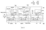
圖7A至圖7C示出本發明一實施例之顯示裝置的修補過程。7A to 7C illustrate a repair process of a display device according to an embodiment of the present invention.
圖7A至圖7C的顯示裝置10F、10F’與圖1A至圖1C的顯示裝置10、10’類似,兩者的差異在於:圖7A至圖7C的多個發光元件LED與圖1A至圖1C的多個發光元件LED不同。The
請參照圖7A,具體而言,在本實施例中,修補用之第二發光元件LED的多個電極240的至少一者的厚度T240-2大於第一發光元件LED1的多個電極240的至少一者的厚度T240-1。請參照圖7A及圖7B,藉此,利用轉置元件1將修補用的第二發光元件LED2轉置到驅動背板100上時,由於第二發光元件LED2的電極240較厚,因此,當轉置元件1下壓,以使第二發光元件LED2與驅動背板100連接時,轉置元件1不易壓傷被保留在驅動背板100上之正常的第一發光元件LED1。Please refer to FIG. 7A. Specifically, in this embodiment, the thickness T240-2 of at least one of the plurality of
請參照圖7C,修補後的顯示裝置10F’的多個發光元件LED包括第一發光元件LED1及第二發光元件LED2。顯示裝置10F’的驅動背板100的多個導電圖案131、132包括第一導電圖案131及第二導電圖案132,第一發光元件LED1及第二發光元件LED2分別電性連接至第一導電圖案131及第二導電圖案132,第一發光元件LED1的頂面LEDa與第一導電圖案131具有第一距離D1,第二發光元件LED2的頂面LEDa與第二導電圖案132具有第二距離D2,且第二距離D2大於第一距離D1。Referring to FIG. 7C , the plurality of light-emitting elements LED of the repaired
在本實施例中,第二發光元件LED2的晶粒D具有第二發光元件LED的頂面LEDa,第一發光元件LED1的晶粒D具有第一發光元件LED1的頂面LEDa,第一發光元件LED1的晶粒D的頂面Da與第一導電圖案131具有第一距離D1,且第二發光元件LED2的晶粒D的頂面Da與第二導電圖案132具有第二距離D2。也就是說,在本實施例中,第二發光元件LED2的晶粒D的頂面Da與第二導電圖案132的距離(即第二距離D2)大於第一發光元件LED1的晶粒D的頂面Da與第一導電圖案131的距離(即第一距離D1),其中第一發光元件LED1的晶粒D的頂面Da及第二發光元件LED2的晶粒D的頂面Da直接接觸於封裝層300。In this embodiment, the die D of the second light-emitting element LED2 has the top surface LEDa of the second light-emitting element LED, and the die D of the first light-emitting element LED1 has the top surface LEDa of the first light-emitting element LED1. There is a first distance D1 between the top surface Da of the die D of the LED1 and the first
前述之圖1A至圖1C、圖2A至圖2C、圖3A至圖3C、圖4A至圖4C、圖5A至圖5C、圖6A至圖6C及圖7A至圖7C的第二發光元件LED2可用以原地修補或異地修補。The second light-emitting element LED2 of the aforementioned Figures 1A to 1C, 2A to 2C, 3A to 3C, 4A to 4C, 5A to 5C, 6A to 6C and 7A to 7C can be used Repair in situ or repair in off-site.
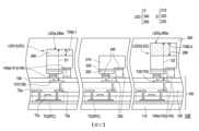
圖8A至圖8C示出本發明一實施例之顯示裝置的修補過程。8A to 8C illustrate a repair process of a display device according to an embodiment of the present invention.
圖8A至圖8C的顯示裝置10G與圖1A至圖1C的顯示裝置10類似,兩者的差異在於:圖8A至圖8C之實施例的驅動背板100G與圖1A至圖1C之實施例的驅動背板100不同。The
請參照圖8A,具體而言,在本實施例中,驅動背板100G的介電層120,設置於接墊層140與基底110之間。特別是,介電層120包括平坦部121及凸出於平坦部121的凸部122。在本實施例中,驅動背板100F之平坦部121所在區域是用以設置首次被轉置於驅動背板100F上的第一發光元件LED1,驅動背板100F之凸部122所在區域是用以異地修補。Please refer to FIG. 8A . Specifically, in this embodiment, the
請參照圖8A,可對顯示裝置10G進行檢測,以檢測已轉置於驅動背板100G上的發光元件LED是否正常。正常的發光元件LED(即第一發光元件LED1)會被保留在驅動背板100G上,而現異常的發光元件(未繪示)則會被移除。之後,再將修補用的發光元件LED(即第二發光元件LED2)轉置到驅動背板100G且令修補用的發光元件LED與驅動背板100電性連接。Referring to FIG. 8A , the
值得注意的是,在本實施例中,修補用的第二發光元件LED2是被轉置到介電層120的凸部122上,因此,當轉置元件1下壓,以使第二發光元件LED2與驅動背板100連接時,轉置元件1不易壓傷被保留在驅動背板100上之正常的第一發光元件LED1。It is worth noting that in this embodiment, the second light-emitting element LED2 for repair is transposed on the
請參照圖8B及圖8C,在完成上述修補動作後,可驅動背板100G上形成封裝層300,以覆蓋第一發光元件LED1及第二發光元件LED2,並完成修補後的顯示裝置10G’。請參照圖8C,顯示裝置10G’之修補用的第二發光元件LED2重疊於介電層120的凸部122,而顯示裝置10G’的第一發光元件LED1重疊於介電層120的平坦部121。顯示裝置10G’的多個發光元件LED包括第一發光元件LED1及第二發光元件LED2。顯示裝置10G’的多個接墊組141、142包括第一接墊組141及第二接墊組142,第一發光元件LED1及第二發光元件LED2分別電性連接至第一接墊組141及第二接墊組142,第二接墊組142的至少一接墊140a與基底110的距離A2大於第一接墊組141的至少一接墊140a與基底110的距離A1。Referring to FIGS. 8B and 8C , after the above repair operation is completed, the
在本實施例中,具有凸部122的介電層120可選擇性位於導電層130與多個畫素驅動電路SPC之間,第二導電圖案132可位於介電層120的凸部122上,第一導電圖案132可位於介電層120的平坦部121上,而第二導電圖案132與基底110的距離B2可大於第一導電圖案131與基底110的距離B1,但本發明不以此為限。在其它實施例中,也可使用其它膜層(例如:介電層150)形成用以設置異地修補之第二發光元件LED2的凸部。In this embodiment, the
10、10’、10A、10A’、10B、10B’、10C、10C’、10D、10D’、10E、10E’、10F、10F’、10G、10G’:顯示裝置 100、100G:驅動背板 110:基底 120、150:介電層 121:平坦部 122:凸部 130:導電層 131、132:導電圖案 140:接墊層 140a:接墊 141、142:接墊組 210:第一型半導體層 220:第二型半導體層 230:主動層 240:電極 250:導電凸塊 260:色轉換圖案 260a、270a、Da、LEDa:頂面 270:透光圖案 300:封裝層 A1、A2、B1、B2:距離 D:晶粒 D1:第一距離 D2:第二距離 LED、LED1、LED2:發光元件 SPC:畫素驅動電路 T2:第二電晶體 T2a:第一端 T2b:第二端 T2c:控制端 T210-1、T210-2、T230-1、T230-2、T240-1、T240-2、T250-1、T250-2、T260、T260-1、T260-2、T270:厚度10, 10’, 10A, 10A’, 10B, 10B’, 10C, 10C’, 10D, 10D’, 10E, 10E’, 10F, 10F’, 10G, 10G’:
圖1A至圖1C示出本發明一實施例之顯示裝置的修補過程。 圖2A至圖2C示出本發明一實施例之顯示裝置的修補過程。 圖3A至圖3C示出本發明一實施例之顯示裝置的修補過程。 圖4A至圖4C示出本發明一實施例之顯示裝置的修補過程。 圖5A至圖5C示出本發明一實施例之顯示裝置的修補過程。 圖6A至圖6C示出本發明一實施例之顯示裝置的修補過程。 圖7A至圖7C示出本發明一實施例之顯示裝置的修補過程。 圖8A至圖8C示出本發明一實施例之顯示裝置的修補過程。1A to 1C illustrate a repair process of a display device according to an embodiment of the present invention. 2A to 2C illustrate a repair process of a display device according to an embodiment of the present invention. 3A to 3C illustrate a repair process of a display device according to an embodiment of the invention. 4A to 4C illustrate a repair process of a display device according to an embodiment of the present invention. 5A to 5C illustrate a repair process of a display device according to an embodiment of the present invention. 6A to 6C illustrate a repair process of a display device according to an embodiment of the present invention. 7A to 7C illustrate a repair process of a display device according to an embodiment of the present invention. 8A to 8C illustrate a repair process of a display device according to an embodiment of the present invention.
10’:顯示裝置10’: Display device
100:驅動背板100:Drive backplane
110:基底110: Base
120、150:介電層120, 150: Dielectric layer
130:導電層130:Conductive layer
131、132:導電圖案131, 132: Conductive pattern
140:接墊層140: Connecting layer
140a:接墊140a: Pad
141、142:接墊組141, 142: Pad group
210:第一型半導體層210: First type semiconductor layer
220:第二型半導體層220: Second type semiconductor layer
230:主動層230:Active layer
240:電極240:Electrode
250:導電凸塊250: Conductive bumps
260:色轉換圖案260: Color conversion pattern
260a、Da、LEDa:頂面260a, Da, LEDa: top surface
300:封裝層300: Encapsulation layer
D:晶粒D: grain
D1:第一距離D1: first distance
D2:第二距離D2: second distance
LED、LED1、LED2:發光元件LED, LED1, LED2: light-emitting components
SPC:畫素驅動電路SPC: pixel drive circuit
T2:第二電晶體T2: Second transistor
T2a:第一端T2a: first end
T2b:第二端T2b: second end
T2c:控制端T2c:Control terminal
Claims (4)
Translated fromChinesePriority Applications (3)
| Application Number | Priority Date | Filing Date | Title |
|---|---|---|---|
| TW110144075ATWI814151B (en) | 2021-11-25 | 2021-11-25 | Display apparatus |
| CN202210345067.3ACN114678389B (en) | 2021-11-25 | 2022-03-31 | Display device |
| US17/991,842US20230163110A1 (en) | 2021-11-25 | 2022-11-21 | Display apparatus |
Applications Claiming Priority (1)
| Application Number | Priority Date | Filing Date | Title |
|---|---|---|---|
| TW110144075ATWI814151B (en) | 2021-11-25 | 2021-11-25 | Display apparatus |
Publications (2)
| Publication Number | Publication Date |
|---|---|
| TW202322084A TW202322084A (en) | 2023-06-01 |
| TWI814151Btrue TWI814151B (en) | 2023-09-01 |
Family
ID=82077002
Family Applications (1)
| Application Number | Title | Priority Date | Filing Date |
|---|---|---|---|
| TW110144075ATWI814151B (en) | 2021-11-25 | 2021-11-25 | Display apparatus |
Country Status (3)
| Country | Link |
|---|---|
| US (1) | US20230163110A1 (en) |
| CN (1) | CN114678389B (en) |
| TW (1) | TWI814151B (en) |
Citations (6)
| Publication number | Priority date | Publication date | Assignee | Title |
|---|---|---|---|---|
| TW202046517A (en)* | 2013-11-18 | 2020-12-16 | 晶元光電股份有限公司 | Light emitting apparatus |
| TW202105797A (en)* | 2019-06-21 | 2021-02-01 | 日商半導體能源研究所股份有限公司 | Display device, display module, electronic device, and manufacturing method of display device |
| CN112928196A (en)* | 2021-01-29 | 2021-06-08 | 厦门天马微电子有限公司 | Display panel, manufacturing method thereof and display device |
| US20210249451A1 (en)* | 2020-02-07 | 2021-08-12 | Samsung Display Co., Ltd. | Method of fabricating conductive pattern, display device, and method of fabricating display device |
| US11133370B2 (en)* | 2019-01-15 | 2021-09-28 | Samsung Display Co., Ltd. | Organic light emitting diode display device and manufacturing method thereof |
| TW202137543A (en)* | 2019-11-12 | 2021-10-01 | 日商半導體能源研究所股份有限公司 | Display unit, display module, electronic device, and method for manufacturing the display unit |
Family Cites Families (11)
| Publication number | Priority date | Publication date | Assignee | Title |
|---|---|---|---|---|
| US9018655B2 (en)* | 2005-02-03 | 2015-04-28 | Epistar Corporation | Light emitting apparatus and manufacture method thereof |
| KR102200058B1 (en)* | 2014-12-19 | 2021-01-08 | 글로 에이비 | Light emitting diode array on a backplane and method of making thereof |
| KR102389346B1 (en)* | 2017-04-03 | 2022-04-25 | 삼성디스플레이 주식회사 | Display device |
| TWI662638B (en)* | 2017-04-21 | 2019-06-11 | 台灣愛司帝科技股份有限公司 | Method and device for repairing a semiconductor chip |
| KR20200043581A (en)* | 2018-10-17 | 2020-04-28 | 삼성디스플레이 주식회사 | Display device |
| TWI690102B (en)* | 2019-01-04 | 2020-04-01 | 友達光電股份有限公司 | Light emitting apparatus and manufacturing method thereof |
| CN113299680B (en)* | 2020-06-05 | 2023-05-12 | 友达光电股份有限公司 | Display device |
| TWI823332B (en)* | 2020-08-24 | 2023-11-21 | 錼創顯示科技股份有限公司 | Spliced micro light emitting diode display panel |
| CN116171495B (en)* | 2020-09-22 | 2025-05-30 | 苏州晶湛半导体有限公司 | Method for manufacturing semiconductor structure |
| CN112786641A (en)* | 2021-01-29 | 2021-05-11 | 錼创显示科技股份有限公司 | Selectively repairable micro light-emitting diode display and repairing method thereof |
| CN113611787B (en)* | 2021-08-02 | 2023-03-14 | 东莞市中麒光电技术有限公司 | Chip transfer structure and Micro LED display module repair method |
- 2021
- 2021-11-25TWTW110144075Apatent/TWI814151B/enactive
- 2022
- 2022-03-31CNCN202210345067.3Apatent/CN114678389B/enactiveActive
- 2022-11-21USUS17/991,842patent/US20230163110A1/enactivePending
Patent Citations (6)
| Publication number | Priority date | Publication date | Assignee | Title |
|---|---|---|---|---|
| TW202046517A (en)* | 2013-11-18 | 2020-12-16 | 晶元光電股份有限公司 | Light emitting apparatus |
| US11133370B2 (en)* | 2019-01-15 | 2021-09-28 | Samsung Display Co., Ltd. | Organic light emitting diode display device and manufacturing method thereof |
| TW202105797A (en)* | 2019-06-21 | 2021-02-01 | 日商半導體能源研究所股份有限公司 | Display device, display module, electronic device, and manufacturing method of display device |
| TW202137543A (en)* | 2019-11-12 | 2021-10-01 | 日商半導體能源研究所股份有限公司 | Display unit, display module, electronic device, and method for manufacturing the display unit |
| US20210249451A1 (en)* | 2020-02-07 | 2021-08-12 | Samsung Display Co., Ltd. | Method of fabricating conductive pattern, display device, and method of fabricating display device |
| CN112928196A (en)* | 2021-01-29 | 2021-06-08 | 厦门天马微电子有限公司 | Display panel, manufacturing method thereof and display device |
Also Published As
| Publication number | Publication date |
|---|---|
| CN114678389A (en) | 2022-06-28 |
| TW202322084A (en) | 2023-06-01 |
| US20230163110A1 (en) | 2023-05-25 |
| CN114678389B (en) | 2025-05-02 |
Similar Documents
| Publication | Publication Date | Title |
|---|---|---|
| US11289633B2 (en) | LED array package and manufacturing method thereof | |
| KR102716902B1 (en) | Display device using micro led and manufacturing method thereof | |
| CN110556455A (en) | Method for manufacturing display module using LED | |
| CN110211987A (en) | Light-emitting-diode panel | |
| TW201826517A (en) | Display panel | |
| US11616096B2 (en) | Display device | |
| CN113594194B (en) | A stacking structure, display screen and display device | |
| CN113380929A (en) | Display panel manufacturing method, display panel and display device | |
| KR20200105843A (en) | Method for manufacturing display device and display device using semiconductor light emitting device | |
| TWI864864B (en) | Display apparatus | |
| CN111864037B (en) | Micro element array substrate, display panel and preparation method thereof | |
| TWI814151B (en) | Display apparatus | |
| CN113451163B (en) | Detection structure and detection method | |
| TWI856355B (en) | Light emitting diode package structure, manufacturing method of light emitting diode package structure and light emitting panel | |
| TWI771248B (en) | Display panel | |
| US20230402465A1 (en) | Pixel array substrate | |
| CN108288629B (en) | Display panel | |
| CN113380766B (en) | LED integrated chip and display device | |
| TWI751672B (en) | Micro led display device and manufacturing method thereof | |
| CN112863387B (en) | A light-emitting display module | |
| CN115347089A (en) | Light-emitting diode packaging structure, manufacturing method and light-emitting panel | |
| TWI776654B (en) | Display apparatus and fabricating method thereof | |
| US20230178681A1 (en) | Method for manufacturing display device | |
| US20240153924A1 (en) | Manufacturing method of electronic device | |
| TW202531572A (en) | Method for manufacturing semiconductor chip |