TWI813496B - Radio frequency circuit and calibration method therefor - Google Patents
Radio frequency circuit and calibration method thereforDownload PDFInfo
- Publication number
- TWI813496B TWI813496BTW111142427ATW111142427ATWI813496BTW I813496 BTWI813496 BTW I813496BTW 111142427 ATW111142427 ATW 111142427ATW 111142427 ATW111142427 ATW 111142427ATW I813496 BTWI813496 BTW I813496B
- Authority
- TW
- Taiwan
- Prior art keywords
- analog converter
- modulator
- current digital
- digital
- radio frequency
- Prior art date
Links
Images


Classifications
- H—ELECTRICITY
- H04—ELECTRIC COMMUNICATION TECHNIQUE
- H04L—TRANSMISSION OF DIGITAL INFORMATION, e.g. TELEGRAPHIC COMMUNICATION
- H04L27/00—Modulated-carrier systems
- H04L27/32—Carrier systems characterised by combinations of two or more of the types covered by groups H04L27/02, H04L27/10, H04L27/18 or H04L27/26
- H04L27/34—Amplitude- and phase-modulated carrier systems, e.g. quadrature-amplitude modulated carrier systems
- H04L27/36—Modulator circuits; Transmitter circuits
- H04L27/362—Modulation using more than one carrier, e.g. with quadrature carriers, separately amplitude modulated
- H04L27/364—Arrangements for overcoming imperfections in the modulator, e.g. quadrature error or unbalanced I and Q levels
- H—ELECTRICITY
- H03—ELECTRONIC CIRCUITRY
- H03M—CODING; DECODING; CODE CONVERSION IN GENERAL
- H03M1/00—Analogue/digital conversion; Digital/analogue conversion
- H03M1/66—Digital/analogue converters
Landscapes
- Engineering & Computer Science (AREA)
- Theoretical Computer Science (AREA)
- Computer Networks & Wireless Communication (AREA)
- Signal Processing (AREA)
- Digital Transmission Methods That Use Modulated Carrier Waves (AREA)
- Circuits Of Receivers In General (AREA)
- Input Circuits Of Receivers And Coupling Of Receivers And Audio Equipment (AREA)
Abstract
Description
Translated fromChinese本發明是關於電子裝置,尤其是關於射頻電路及其校正方法。The present invention relates to electronic devices, and in particular to radio frequency circuits and correction methods thereof.
正交振幅調變(Quadrature Amplitude Modulation,QAM)常用於無線裝置中,而無線裝置之射頻電路常會遭遇同相(in-phase)路徑(以下簡稱為I路徑)與正交(quadrature-phase)路徑(以下簡稱為Q路徑)不平衡(即,同相與正交之間不平衡(In-phase Quadrature-phase imbalance))的問題,簡稱為IQ不平衡(IQ imbalance)。而IQ不平衡(尤其是不匹配的直流偏置(DC offset))會導致射頻電路之本地振盪器(local oscillator,LO)訊號的洩漏(leakage)。Quadrature Amplitude Modulation (QAM) is commonly used in wireless devices, and the radio frequency circuits of wireless devices often encounter in-phase paths (hereinafter referred to as I paths) and quadrature-phase paths ( The problem of Q path imbalance (ie, imbalance between in-phase and quadrature (In-phase Quadrature-phase imbalance)) is referred to as IQ imbalance for short. IQ imbalance (especially mismatched DC offset) will cause leakage of the local oscillator (LO) signal of the RF circuit.
鑑於先前技術之不足,本發明之一目的在於提供一種射頻電路及其校正方法,以改善先前技術的不足。In view of the shortcomings of the prior art, one objective of the present invention is to provide a radio frequency circuit and a correction method thereof to improve the shortcomings of the prior art.
本發明之一實施例提供一種射頻電路的校正方法,該射頻電路包含一同相路徑及一正交路徑,該同相路徑包含一第一調變器及一第一元件,該正交路徑包含一第二調變器及一第二元件,該第一調變器、該第二調變器、該第一元件及該第二元件分別包含一第一電流數位類比轉換器、一第二電流數位類比轉換器、一第三電流數位類比轉換器及一第四電流數位類比轉換器。該校正方法包含:校正該第一調變器及該第二調變器之直流偏移,以得到用於該第一電流數位類比轉換器及該第二電流數位類比轉換器之一第一目標設定值;交換該同相路徑及該正交路徑,然後再次校正該第一調變器及該第二調變器之該直流偏移,以得到用於該第一電流數位類比轉換器及該第二電流數位類比轉換器之一第二目標設定值;以該第一目標設定值及該第二目標設定值之一函數值設定該第一電流數位類比轉換器及該第二電流數位類比轉換器;校正該第一元件及該第二元件之直流偏移,以得到用於該第三電流數位類比轉換器及該第四電流數位類比轉換器之一第三目標設定值;校正該第一調變器及該第二調變器之該直流偏移,以得到用於該第一電流數位類比轉換器及該第二電流數位類比轉換器之一第四目標設定值;以及,校正該第一元件及該第二元件之該直流偏移,以得到用於該第三電流數位類比轉換器及該第四電流數位類比轉換器之一第五目標設定值。An embodiment of the present invention provides a method for calibrating a radio frequency circuit. The radio frequency circuit includes an in-phase path and a quadrature path. The in-phase path includes a first modulator and a first element. The quadrature path includes a first modulator. Two modulators and a second component. The first modulator, the second modulator, the first component and the second component respectively include a first current digital-to-analog converter and a second current digital analog converter.a bit-to-analog converter, a third current to digital-to-analog converter and a fourth current to digital-to-analog converter. The correction method includes: correcting the DC offset of the first modulator and the second modulator to obtain a first target for the first current digital-to-analog converter and the second current digital-to-analog converter. Set value; exchange the in-phase path and the quadrature path, and then correct the DC offset of the first modulator and the second modulator again to obtain the value for the first current digital-to-analog converter and the third A second target setting value of two current digital to analog converters; setting the first current to digital to analog converter and the second current to digital to analog converter with a function value of the first target setting value and the second target setting value ;Correcting the DC offset of the first element and the second element to obtain a third target setting value for the third current digital-to-analog converter and the fourth current digital-to-analog converter; correcting the first adjustment the DC offset of the converter and the second modulator to obtain a fourth target setting value for the first current digital-to-analog converter and the second current digital-to-analog converter; and, correcting the first The DC offset of the component and the second component is used to obtain a fifth target setting value for the third current digital-to-analog converter and the fourth current current digital-to-analog converter.
本發明之另一實施例提供一種射頻電路。射頻電路包含一同相路徑、一正交路徑及一控制電路,該同相路徑包含一第一調變器及一第一元件,該正交路徑包含一第二調變器及一第二元件,該第一調變器、該第二調變器、該第一元件及該第二元件分別包含一第一電流數位類比轉換器、一第二電流數位類比轉換器、一第三電流數位類比轉換器及一第四電流數位類比轉換器。該控制電路執行以下步驟以校正該射頻電路:校正該第一調變器及該第二調變器之直流偏移,以得到用於該第一電流數位類比轉換器及該第二電流數位類比轉換器之一第一目標設定值;交換該同相路徑及該正交路徑,然後再次校正該第一調變器及該第二調變器之該直流偏移,以得到用於該第一電流數位類比轉換器及該第二電流數位類比轉換器之一第二目標設定值;以該第一目標設定值及該第二目標設定值之一函數值設定該第一電流數位類比轉換器及該第二電流數位類比轉換器;校正該第一元件及該第二元件之直流偏移,以得到用於該第三電流數位類比轉換器及該第四電流數位類比轉換器之一第三目標設定值;校正該第一調變器及該第二調變器之該直流偏移,以得到用於該第一電流數位類比轉換器及該第二電流數位類比轉換器之一第四目標設定值;以及,校正該第一元件及該第二元件之該直流偏移,以得到用於該第三電流數位類比轉換器及該第四電流數位類比轉換器之一第五目標設定值。Another embodiment of the present invention provides a radio frequency circuit. The radio frequency circuit includes an in-phase path, a quadrature path and a control circuit. The in-phase path includes a first modulator and a first element. The quadrature path includes a second modulator and a second element. The first modulator, the second modulator, the first element and the second element respectively include a first current digital to analog converter, a second current digital to analog converter and a third current digital to analog converter. and a fourth current digital-to-analog converter. The control circuit performs the following steps to calibrate the radio frequency circuit: calibrate the DC offset of the first modulator and the second modulator to obtain the DC offset for the first current-to-digital analog converter and the second current-to-digital analog converter. A first target setting value of the converter; swapping the in-phase path and the quadrature path, and then correcting the DC offset of the first modulator and the second modulator again to obtain the first current Digital classA second target setting value of the ratio converter and the second current digital-to-analog converter; setting the first current digital-to-analog converter and the third current digital-to-analog converter with a function value of the first target setting value and the second target setting value. Two current digital-to-analog converters; correcting the DC offset of the first element and the second element to obtain a third target setting value for the third current digital-to-analog converter and the fourth current digital-to-analog converter ;Correcting the DC offset of the first modulator and the second modulator to obtain a fourth target setting value for the first current digital-to-analog converter and the second current digital-to-analog converter; And, correcting the DC offset of the first element and the second element to obtain a fifth target setting value for the third current digital-to-analog converter and the fourth current digital-to-analog converter.
本發明之實施例所體現的技術手段可以改善先前技術之缺點的至少其中之一,因此本發明相較於先前技術可以校正射頻電路之IQ不平衡,減少本地振盪訊號的洩漏。The technical means embodied in the embodiments of the present invention can improve at least one of the shortcomings of the prior art. Therefore, compared with the prior art, the present invention can correct the IQ imbalance of the radio frequency circuit and reduce the leakage of the local oscillation signal.
有關本發明的特徵、實作與功效,茲配合圖式作實施例詳細說明如下。The features, implementation and effects of the present invention are described in detail below with reference to the drawings and examples.
100,1000:電子裝置100,1000: Electronic devices
101,1001:射頻電路101,1001:RF circuit
102:控制電路102:Control circuit
110:同相路徑110: In-phase path
112,122:DAC(數位類比轉換器)112,122: DAC (digital to analog converter)
114,124,1014,1024:LPF(低通濾波器)114,124,1014,1024:LPF (low pass filter)
116,126:調變器116,126:Modulator
120:正交路徑120: Orthogonal path
130:回授路徑130: Feedback path
132:ADC(類比數位轉換器)132:ADC (analog-to-digital converter)
134:PGA(功率增益放大器)134:PGA (power gain amplifier)
136:自混頻器136:Self mixer
140:加法電路140:Adder circuit
150:PAD(功率放大器驅動器)150:PAD (power amplifier driver)
160:PA(功率放大器)160:PA (power amplifier)
170:LO(本地振盪器)170:LO (local oscillator)
PSD:功率頻譜密度PSD: power spectral density
103:PSD量測電路103:PSD measurement circuit
SF:回授訊號SF: feedback signal
CD1,CD2,CD_A1,CD_A5,CD_A2,CD_A3,CD_A4,CD_B1,CD_B5,CD_B2,CD_B3,CD_B4:數位碼CD1, CD2, CD_A1, CD_A5, CD_A2, CD_A3, CD_A4, CD_B1, CD_B5, CD_B2, CD_B3, CD_B4: digital code
ID1,ID2,ID3,ID4,ID5,ID6:電流數位類比轉換器ID1, ID2, ID3, ID4, ID5, ID6: current digital to analog converter
SS1:第一校正區間SS1: first correction interval
SS2:第二校正區間SS2: second correction interval
SS1':第三校正區間SS1': The third correction interval
SS2':第四校正區間SS2': The fourth correction interval
1018,1028:緩衝器1018,1028: buffer
A_Die:類比晶粒A_Die: analog grain
D_Die:數位晶粒D_Die:Digital die
405,S410,S420,S430,S435,S440,S450,S460,S610,S710,S720,S730,S740:步驟405,S410,S420,S430,S435,S440,S450,S460,S610,S710,S720,S730,S740: Steps
圖1A是本發明電子裝置之一實施例的功能方塊圖。FIG. 1A is a functional block diagram of an embodiment of an electronic device of the present invention.
圖1B顯示調變器及低通濾波器各包含一個電流數位類比轉換器。Figure 1B shows that the modulator and low-pass filter each include a current digital-to-analog converter.
圖2顯示電流數位類比轉換器的直流偏置與數位碼的理想關係圖。Figure 2 shows an ideal plot of DC offset versus digital code for a current-to-digital analog converter.
圖3及圖4顯示電流數位類比轉換器的直流偏置與數位碼的實際關係圖。Figures 3 and 4 show the actual relationship between the DC bias and the digital code of the current digital-to-analog converter.
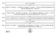
圖5A及圖5B顯示本發明射頻電路的校正方法之一實施例的流程圖。FIG. 5A and FIG. 5B show a flow chart of an embodiment of the calibration method of the radio frequency circuit of the present invention.
圖6顯示校正步驟之一實施例的細節。Figure 6 shows details of one embodiment of the correction step.
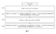
圖7顯示本發明射頻電路的校正方法之另一實施例的流程圖。FIG. 7 shows a flow chart of another embodiment of the radio frequency circuit calibration method of the present invention.
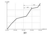
圖8及圖9顯示電流數位類比轉換器的直流偏置與數位碼的實際關係圖。Figures 8 and 9 show the actual relationship between the DC bias and the digital code of the current digital-to-analog converter.
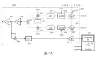
圖10A是本發明電子裝置之另一實施例的功能方塊圖。FIG. 10A is a functional block diagram of another embodiment of the electronic device of the present invention.
圖10B顯示調變器及緩衝器各包含一個電流數位類比轉換器。Figure 10B shows that the modulator and buffer each include a current digital-to-analog converter.
以下說明內容之技術用語係參照本技術領域之習慣用語,如本說明書對部分用語有加以說明或定義,該部分用語之解釋係以本說明書之說明或定義為準。The technical terms used in the following description refer to the idioms in the technical field. If some terms are explained or defined in this specification, the explanation or definition of these terms shall prevail.
本發明之揭露內容包含射頻電路及其校正方法。由於本發明之射頻電路所包含之部分元件單獨而言可能為已知元件,因此在不影響該裝置發明之充分揭露及可實施性的前提下,以下說明對於已知元件的細節將予以節略。此外,本發明之射頻電路的校正方法的部分或全部流程可以是軟體及/或韌體之形式,並且可藉由本發明之控制電路或其等效裝置來執行,在不影響該方法發明之充分揭露及可實施性的前提下,以下方法發明之說明將著重於步驟內容而非硬體。The disclosure of the present invention includes radio frequency circuits and calibration methods thereof. Since some of the components included in the radio frequency circuit of the present invention may be known components individually, the details of the known components will be omitted in the following description without affecting the full disclosure and implementability of the device invention. In addition, part or all of the process of the radio frequency circuit calibration method of the present invention can be in the form of software and/or firmware, and can be executed by the control circuit of the present invention or its equivalent device, without affecting the fullness of the method invention. Under the premise of disclosure and implementability, the following description of the method invention will focus on the step content rather than the hardware.
圖1A是本發明電子裝置之一實施例的功能方塊圖。電子裝置100包含射頻電路101及控制電路102。射頻電路101包含同相路徑110、正交路徑120、回授路徑130、加法電路140、功率放大器驅動器(power amplifier driver,PAD)150、功率放大器(power amplifier,PA)160以及本地振盪器(local oscillator,LO)170。同相路徑110包含數位類比轉換器(digital-to-analog converter,DAC)112、低通濾波器(low-pass filter,LPF)114以及調變器(或稱為混頻器(mixer))116。正交路徑120包含DAC 122、LPF 124以及調變器126。回授路徑130包含類比數位轉換器(analog-to-digital converter,ADC)132、功率增益放大器(Power Gain Amplifier,PGA)134以及自混頻器(self-mixer)136。射頻電路101的原理及操作細節為本技術領域具有通常知識者所熟知,故不再贅述。FIG. 1A is a functional block diagram of an embodiment of an electronic device of the present invention. The
控制電路102包含功率譜密度(power spectral density,PSD)量測電路103。PSD量測電路103用來量測回授訊號SF的功率頻譜密度。控制電路102根據PSD量測電路103所輸出的功率頻譜密度PSD來調整(或產生)數位碼CD1及數位碼CD2。控制電路102透過數位碼CD1設定調變器116及調變器126的電流數位類比轉換器(Current Digital-to-Analog Converter,IDAC)。控制電路102透過數位碼CD2設定LPF 114及LPF 124的電流數位類比轉換器。The
請參閱圖1B,圖1B顯示調變器116、調變器126、LPF 114及LPF 124各包含一個電流數位類比轉換器(分別為電流數位類比轉換器ID1、電流數位類比轉換器ID2、電流數位類比轉換器ID3及電流數位類比轉換器ID4)。電流數位類比轉換器的細部電路及操作原理為本技術領域具有通常知識者所熟知,故不再贅述。理想上,該些電流數位類比轉換器的直流偏置(DC offset)與數位碼(即,設定值)的關係是線性的(如圖2所示)。然而,因為製程變異(process variation)等因素,該些元件的實際的直流偏置與數位碼的關係可能是非線性的。舉例來說,調變器116的電流數位類比轉換器ID1的特性與調變器126的電流數位類比轉換器ID2的特性可能是非線性的(以圖3作為代表,然兩者實際上可能有些微差異),而IPF 114的電流數位類比轉換器ID3的特性與LPF 124的電流數位類比轉換器ID4的特性可能是非線性的(以圖4作為代表,然兩者實際上可能有些微差異)。因此,必須對LPF 114、調變器116、LPF 124及調變器126進行校正(例如,藉由調整數位碼),以使同相路徑110與正交路徑120在直流偏置上更為匹配(例如,更接近目標值),防止LO 170之本地振盪器訊號的洩漏。Please refer to Figure 1B. Figure 1B shows that the
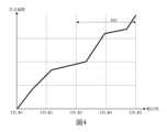
請參閱圖3,對調變器116及調變器126而言,電流數位類比轉換器的數位碼的最小值及最大值分別為數位碼CD_A1與數位碼CD_A5。數位碼CD_A2、數位碼CD_A3及數位碼CD_A4可以分別約為數位碼CD_A5的1/4、2/4及3/4。請參閱圖4,對LPF 114及LPF 124而言,電流數位類比轉換器的數位碼的最小值及最大值分別為數位碼CD_B1與數位碼CD_B5。數位碼CD_B2、數位碼CD_B3及數位碼CD_B4可以分別約為數位碼CD_B5的1/4、2/4及3/4。Referring to FIG. 3 , for the
圖3及圖4將數位碼劃分為4個區間;然而,這僅用於示例而非用以限定本發明。在一個不同的實施例中,數位碼可以被劃分為N個區間(N為大於等於2之整數)。Figures 3 and 4 divide the digital code into four intervals; however, this is only used as an example and does not limit the present invention. In a different embodiment, the digital code may be divided into N intervals (N is an integer greater than or equal to 2).
需注意的是,請參閱圖3及圖4,LPF 114(124)的電流數位類比轉換器的數位碼的範圍([CD_A1,CD_A5])可能等於或不等於調變器116(126)的電流數位類比轉換器的數位碼的範圍([CD_B1,CD_B5])。舉例來說,假設LPF 114(124)的電流數位類比轉換器的數位碼為X個位元(即,CD_A5=2X-1),且調變器116(126)的電流數位類比轉換器的數位碼為Y個位元(即,CD_B5=2Y-1),則X=Y或X≠Y(X及Y為大於等於2之整數)。It should be noted that, please refer to Figure 3 and Figure 4, the range of the digital code of the current digital-to-analog converter of LPF 114 (124) ([CD_A1, CD_A5]) may or may not be equal to the current of the modulator 116 (126) The range of digital codes of the digital-to-analog converter ([CD_B1, CD_B5]). For example, assume that the digital code of the current digital-to-analog converter of LPF 114 (124) isX bits (i.e., CD_A5=2 The digital code is Y bits (ie, CD_B5=2Y -1), then X=Y or X≠Y (X and Y are integers greater than or equal to 2).
圖5A、圖5B及圖6顯示本發明射頻電路的校正方法之一實施例的流程圖,包含以下步驟。FIG. 5A, FIG. 5B and FIG. 6 show a flow chart of an embodiment of a calibration method for a radio frequency circuit of the present invention, which includes the following steps.
步驟S405:控制電路102決定第一校正區間SS1。更明確地說,請參閱圖3,控制電路102根據數位碼的範圍(即,[CD_A1,CD_A5])決定第一校正區間SS1。第一校正區間SS1可以是數位碼的全部範圍(即,SS1=[CD_A1,CD_A5])或是局部範圍(例如,SS1=[CD_A1,CD_A4]或SS1=[CD_A3,CD_A5])。在圖3的例子中,第一校正區間SS1是[CD_A1,CD_A3](即,CD_A1≦CD1≦CD_A3)。在一些實施例中,控制電路102根據經驗或調變器116(126)的特性來決定第一校正區間SS1。Step S405: The
步驟S410:控制電路102根據第一校正區間SS1,校正調變器116之直流偏移及調變器126之直流偏移,以得到用於電流數位類比轉換器ID1及電流數位類比轉換器ID2的第一目標設定值(CT1)。在一些實施例中,步驟S410包含調低LPF 114與LPF 124的增益(例如調至最小值),以降低LPF 114與LPF 124對訊號的影響。Step S410: The
請參閱圖6,圖6顯示步驟S410的實施細節的一實施例。Please refer to FIG. 6 , which shows an embodiment of implementation details of step S410.
步驟S610:在該校正區間(例如,第一校正區間SS1)內,控制電路102以內插法或掃描全部數位碼的方式找出數位碼CD1的目標設定值(例如,步驟S410之第一目標設定值(CT1))。目標設定值對應於相對小的鏡像訊號(即,鏡像訊號的功率頻譜密度PSD相對小)。Step S610: In the correction interval (for example, the first correction interval SS1), the
請繼續參閱圖5A。Please continue to see Figure 5A.
步驟S420:控制電路102交換(swap)I路徑及Q路徑,然後根據第一校正區間SS1,再次校正調變器116之直流偏移及調變器126之直流偏移,以得到用於電流數位類比轉換器ID1及電流數位類比轉換器ID2的第二目標設定值(CT2)。步驟S420與步驟S410相似(即,步驟S420的實施細節可以參考步驟S610),但控制電路102先控制I路徑及Q路徑交換(例如,藉由控制LPF 114/124或調變器116/126的開關),再進行校正操作。交換I路徑與Q路徑的目的在於排除前級的元件(例如,基頻電路(圖未示))的直流偏移,此為本技術領域具有通常知識者所熟知,故不再贅述。Step S420: The
類似地,在一些實施例中,步驟S420包含調低LPF 114與LPF 124的增益。Similarly, in some embodiments, step S420 includes reducing the gains of
步驟S430:控制電路102以第一目標設定值(CT1)及第二目標設定值(CT2)之一函數值(例如平均值或與其近似之函數值)設定調變器116的電流數位類比轉換器ID1及調變器126的電流數位類比轉換器ID2。舉例來說,控制電路102以(CT1+CT2)/2設定電流數位類比轉換器ID1及電流數位類比轉換器ID2,如此可以排除前級的元件的直流偏移,以避免其影響射頻電路101的校正。Step S430: The
步驟S435:控制電路102決定第二校正區間SS2。步驟S435與步驟S405類似。請參考圖4,在圖4的例子中,第二校正區間SS2是[CD_B3,CD_B5](即,CD_B3≦CD2≦CD_B5)。在一些實施例中,控制電路102根據經驗或LPF 114(124)的特性來決定第二校正區間SS2。Step S435: The
步驟S440:控制電路102根據第二校正區間SS2校正LPF 114之直流偏移及LPF 124之直流偏移,以得到用於電流數位類比轉換器ID3及電流數位類比轉換器ID4的第三目標設定值(CT3)。類似於步驟S410,步驟S440的實施細節可以參考步驟S610。在一些實施例中,若控制電路102在步驟S410及步驟S420中調低LPF 114與LPF 124的增益,則控制電路102在步驟S440中調高LPF 114與LPF 124的增益(例如調至最大值)。Step S440: The
以下的討論請參閱圖5B。由於步驟S440對LPF 114及LPF 124進行了校正,所以需要再次校正調變器116及調變器126(步驟S450)。再者,由於步驟S450對調變器116及調變器126進行了校正,所以需要再次校正LPF 114及LPF 124(步驟S460)。See Figure 5B for discussion below. Since the
步驟S450:控制電路102根據第一校正區間SS1校正調變器116及調變器126之直流偏移,以得到用於電流數位類比轉換器ID1及電流數位類比轉換器ID2的第四目標設定值(CT4)。步驟S450的實施細節可以參考步驟S610。類似地,在一些實施例中,步驟S450包含調低LPF 114與LPF 124的增益。Step S450: The
步驟S460:控制電路102根據第二校正區間SS2校正LPF 114及LPF 124之直流偏移,以得到用於電流數位類比轉換器ID3及電流數位類比轉換器ID4的第五目標設定值(CT5)。步驟S460的實施細節可以參考步驟S610。在一些實施例中,若控制電路102在步驟S450中調低LPF 114與LPF 124的增益,則控制電路102在步驟S460中調高LPF 114與LPF 124的增益。Step S460: The
綜上所述,經過二次校正調變器116及調變器126(包含步驟S410~步驟S430以及步驟S450)以及二次校正LPF 114及LPF 124(包含步驟S440以及步驟S460),射頻電路101的IQ不平衡可以得到校正,減少本地振盪訊號的洩漏。In summary, after the secondary correction of the
圖7顯示本發明射頻電路的校正方法之另一實施例的流程圖,包含以下步驟。FIG. 7 shows a flow chart of another embodiment of the calibration method of a radio frequency circuit of the present invention, which includes the following steps.
步驟S405~S440:請參考圖5A的流程圖及相關的說明。Steps S405~S440: Please refer to the flow chart in Figure 5A and related descriptions.
步驟S710:控制電路102根據該平均值(即,步驟S430的平均值(CT1+CT2)/2)決定第三校正區間SS1',第三校正區間SS1'小於步驟S410及步驟S420的第一校正區間SS1(即,SS1'<SS1)。更明確地說,請參閱圖8(圖8對應於圖3),圖8的例子假設平均值((CT1+CT2)/2)大於數位碼CD_A2(即,CD_A2<(CT1+CT2)/2≦CD_A3),因此控制電路102決定第三校正區間SS1'為[CD_A2,CD_A3]。然而,如果平均值((CT1+CT2)/2)小於等於數位碼CD_A2(即,CD_A1≦(CT1+CT2)/2≦CD_A2),則控制電路102決定第三校正區間SS1'為[CD_A1,CD_A2]。Step S710: The
步驟S720:控制電路102根據第三校正區間SS1',校正調變器116之直流偏移及調變器126之直流偏移,以得到用於電流數位類比轉換器ID1及電流數位類比轉換器ID2的第四目標設定值(CT4)。步驟S720與步驟S450相似,差別在於步驟S720是根據第三校正區間SS1'進行校正(即,對圖8的例子而言,CD_A2≦CD1≦CD_A3)。由於第三校正區間SS1'小於第一校正區間SS1(即,候選的數位碼變少),所以相較於步驟S450,步驟S720可以更快得到第四目標設定值(CT4),而且內插法也會更為準確(即,第四目標設定值(CT4)更為準確)。Step S720: The
步驟S730:控制電路102根據第三目標設定值(CT3)決定第四校正區間SS2'。步驟S730與步驟S710相似。第四校正區間SS2'小於步驟S440的第二校正區間SS2(即,SS2'<SS2)。更明確地說,請參閱圖9(圖9對應於圖4),圖9的例子假設第三目標設定值(CT3)小於等於CD_B4(即,CD_B3≦CT3≦CD_B4),因此控制電路102決定第四校正區間SS2'為[CD_B3,CD_B4]。Step S730: The
步驟S740:控制電路102根據第四校正區間SS2',校正LPF 114之直流偏移及LPF 124之直流偏移,以得到用於電流數位類比轉換器ID3及電流數位類比轉換器ID4的第五目標設定值(CT5)。步驟S740與步驟S460相似,差別在於步驟S740是根據第四校正區間SS2'進行校正(即,對圖9的例子而言,CD_B3≦CD2≦CD_B4)。相較於步驟S460,步驟S740可以更快得到第五目標設定值(CT5),而且內插法也會更為準確(即,第五目標設定值(CT5)更為準確)。Step S740: The
綜上所述,在圖7的實施例中,因為第二次校正(即,步驟S720或步驟S740)所使用的校正區間(即,第三校正區間SS1'或第四校正區間SS2')小於第一次校正(即,步驟S410~步驟S420或步驟S440)所使用的校正區間(即,第一校正區間SS1或第二校正區間SS2),所以第二次校正會更快收斂(即,更快得到第四目標設定值(CT4)或第五目標設定值(CT5)),加速射頻電路101之整體的校正流程。To sum up, in the embodiment of FIG. 7 , because the correction interval (ie, the third correction interval SS1 ′ or the fourth correction interval SS2 ′) used in the second correction (ie, step S720 or step S740 ) is smaller than The correction interval (ie, the first correction interval SS1 or the second correction interval SS2) used in the first correction (ie, step S410 to step S420 or step S440), so the second correction will converge faster (ie, more accurate The fourth target setting value (CT4) or the fifth target setting value (CT5) is obtained quickly, thereby accelerating the overall calibration process of the
請參閱圖10A,圖10A是本發明電子裝置之另一實施例的功能方塊圖。電子裝置1000與電子裝置100相似,差別在於LPF 1014及LPF 1024是被動式元件(不包含電流數位類比轉換器),而且射頻電路1001的同相路徑110及正交路徑120分別更包含緩衝器1018及緩衝器1028。電子裝置1000是類比晶粒(analog die)A_Die與數位晶粒(digital die)D_Die的組合,而緩衝器1018及緩衝器1028是用來確保數位晶粒D_Die與類比晶粒A_Die之間的資料傳輸正確。Please refer to FIG. 10A , which is a functional block diagram of an electronic device according to another embodiment of the present invention. The
請參閱圖10B,圖10B顯示調變器116、調變器126、緩衝器1018及緩衝器1028各包含一個電流數位類比轉換器(分別為電流數位類比轉換器ID1、電流數位類比轉換器ID2、電流數位類比轉換器ID5及電流數位類比轉換器ID6)。Please refer to Figure 10B, Figure 10B shows
因為緩衝器1018及緩衝器1028包含電流數位類比轉換器,所以圖10A的射頻電路1001也可以根據上述的校正方法校正。更明確地說,當圖5A~圖5B或圖7的校正方法應用於射頻電路1001時,只需以緩衝器1018與緩衝器1028分別取代步驟S440、步驟S460及步驟S740中的LPF 114與LPF 124,以及以電流數位類比轉換器ID5與電流數位類比轉換器ID6分別取代電流數位類比轉換器ID3與電流數位類比轉換器ID4即可。Because the
請注意,只要縮減第一校正區間SS1及第二校正區間SS2的其中一者就可以加速射頻電路101或射頻電路1001之整體的校正流程及/或提高內插法的準確度。換言之,在一個不同的實施例中,控制電路102執行步驟S405~步驟S440、步驟S710、步驟S720以及步驟S460(即,只把第一校正區間SS1縮減為第三校正區間SS1',但不縮減第二校正區間SS2)。在另一個不同的實施例中,控制電路102執行步驟S405~步驟S440、步驟S450、步驟S730及步驟S740(即,只把第二校正區間SS2縮減為第四校正區間SS2',但不縮減第一校正區間SS1)。Please note that as long as one of the first correction interval SS1 and the second correction interval SS2 is reduced, the overall correction process of the
本技術領域具有通常知識者可以根據以上的揭露內容來設計控制電路102,也就是說,控制電路102可以是特殊應用積體電路(Application Specific Integrated Circuit,ASIC)或是由可程式化邏輯裝置(Programmable Logic Device,PLD)等電路或硬體實作。Those skilled in the art can design the
前揭實施例雖以調變器、低通濾波器及緩衝器為例,然此並非對本發明之限制,本技術領域人士可依本發明之揭露適當地將本發明應用於其它具有電流數位類比轉換器的元件。Although the aforementioned embodiments take modulators, low-pass filters and buffers as examples, they are notWith regard to the limitations of the present invention, those skilled in the art can appropriately apply the present invention to other devices with current digital-to-analog converters based on the disclosure of the present invention.
由於本技術領域具有通常知識者可藉由本案之裝置發明的揭露內容來瞭解本案之方法發明的實施細節與變化,因此,為避免贅文,在不影響該方法發明之揭露要求及可實施性的前提下,重複之說明在此予以節略。請注意,前揭圖示中,元件之形狀、尺寸及比例僅為示意,係供本技術領域具有通常知識者瞭解本發明之用,非用以限制本發明。此外,在一些實施例中,前揭的流程圖中所提及的步驟可依實際操作調整其前後順序,甚至可同時或部分同時執行。Since those with ordinary knowledge in the technical field can understand the implementation details and changes of the method invention through the disclosure of the device invention in this case, therefore, in order to avoid redundancy, the disclosure requirements and implementability of the method invention will not be affected. Under the premise, repeated explanations are omitted here. Please note that the shapes, sizes and proportions of the components in the foregoing figures are only illustrative and are intended for those with ordinary knowledge in the art to understand the present invention and are not intended to limit the present invention. In addition, in some embodiments, the order of the steps mentioned in the above-mentioned flow chart can be adjusted according to the actual operation, and can even be executed simultaneously or partially simultaneously.
雖然本發明之實施例如上所述,然而該些實施例並非用來限定本發明,本技術領域具有通常知識者可根據本發明之明示或隱含之內容對本發明之技術特徵施以變化,凡此種種變化均可能屬於本發明所尋求之專利保護範疇,換言之,本發明之專利保護範圍須視本說明書之申請專利範圍所界定者為準。Although the embodiments of the present invention are described above, these embodiments are not intended to limit the present invention. Those with ordinary skill in the art may make changes to the technical features of the present invention based on the explicit or implicit contents of the present invention. All these changes may fall within the scope of patent protection sought by the present invention. In other words, the patent protection scope of the present invention must be determined by the patent application scope of this specification.
S405,S410,S420,S430,S435,S440:步驟S405, S410, S420, S430, S435, S440: steps
Claims (10)
Translated fromChinesePriority Applications (2)
| Application Number | Priority Date | Filing Date | Title |
|---|---|---|---|
| TW111142427ATWI813496B (en) | 2022-11-07 | 2022-11-07 | Radio frequency circuit and calibration method therefor |
| US18/374,365US12309018B2 (en) | 2022-11-07 | 2023-09-28 | Radio frequency circuit and calibration method therefor |
Applications Claiming Priority (1)
| Application Number | Priority Date | Filing Date | Title |
|---|---|---|---|
| TW111142427ATWI813496B (en) | 2022-11-07 | 2022-11-07 | Radio frequency circuit and calibration method therefor |
Publications (2)
| Publication Number | Publication Date |
|---|---|
| TWI813496Btrue TWI813496B (en) | 2023-08-21 |
| TW202420729A TW202420729A (en) | 2024-05-16 |
Family
ID=88586070
Family Applications (1)
| Application Number | Title | Priority Date | Filing Date |
|---|---|---|---|
| TW111142427ATWI813496B (en) | 2022-11-07 | 2022-11-07 | Radio frequency circuit and calibration method therefor |
Country Status (2)
| Country | Link |
|---|---|
| US (1) | US12309018B2 (en) |
| TW (1) | TWI813496B (en) |
Cited By (1)
| Publication number | Priority date | Publication date | Assignee | Title |
|---|---|---|---|---|
| TWI874182B (en)* | 2024-04-11 | 2025-02-21 | 瑞昱半導體股份有限公司 | Electronic device, communication chip, and transmitter power ramping control thereof |
Families Citing this family (1)
| Publication number | Priority date | Publication date | Assignee | Title |
|---|---|---|---|---|
| TWI813496B (en)* | 2022-11-07 | 2023-08-21 | 瑞昱半導體股份有限公司 | Radio frequency circuit and calibration method therefor |
Citations (3)
| Publication number | Priority date | Publication date | Assignee | Title |
|---|---|---|---|---|
| US20040224715A1 (en)* | 2003-05-07 | 2004-11-11 | Rosenlof John R. | System and method for correcting transmitter impairments |
| US8184740B2 (en)* | 2006-04-21 | 2012-05-22 | Nec Corporation | Signal processing circuit |
| TW202243419A (en)* | 2021-04-23 | 2022-11-01 | 瑞昱半導體股份有限公司 | Transmitter circuit, compensation value calibration device and method for calibrating iq imbalance compensation values |
Family Cites Families (62)
| Publication number | Priority date | Publication date | Assignee | Title |
|---|---|---|---|---|
| US4843351A (en)* | 1987-08-28 | 1989-06-27 | Hewlett-Packard Company | Vector modulation signal generator |
| US6154158A (en)* | 1998-06-30 | 2000-11-28 | Qualcomm Incorporated | Digital-to-analog converter D.C. offset correction comparing converter input and output signals |
| US7558556B1 (en)* | 1999-10-21 | 2009-07-07 | Broadcom Corporation | Adaptive radio transceiver with subsampling mixers |
| US7095348B1 (en)* | 2000-05-23 | 2006-08-22 | Marvell International Ltd. | Communication driver |
| US7194037B1 (en)* | 2000-05-23 | 2007-03-20 | Marvell International Ltd. | Active replica transformer hybrid |
| US6763227B2 (en)* | 2001-11-07 | 2004-07-13 | Texas Instruments Incorporated | Systems and methods for modulator calibration |
| US7363563B1 (en)* | 2003-12-05 | 2008-04-22 | Pmc-Sierra, Inc. | Systems and methods for a built in test circuit for asynchronous testing of high-speed transceivers |
| US7532870B2 (en)* | 2004-04-13 | 2009-05-12 | Maxlinear, Inc. | Method and apparatus for DC offset removal |
| US20060255997A1 (en)* | 2005-04-08 | 2006-11-16 | M/A-Com, Inc. And M/A-Com Eurotec Bv | Differential analog filter |
| US7733949B2 (en)* | 2005-12-07 | 2010-06-08 | Cisco Technology, Inc. | Wireless communications system with reduced sideband noise and carrier leakage |
| JP2009531924A (en)* | 2006-03-28 | 2009-09-03 | エヌエックスピー ビー ヴィ | Transmitter with delay mismatch compensation |
| US7634027B2 (en)* | 2006-12-06 | 2009-12-15 | Broadcom Corporation | Method and system for independent I and Q loop amplitude control for quadrature generators |
| US20080181337A1 (en)* | 2007-01-31 | 2008-07-31 | Silicon Laboratories, Inc. | Spur and Distortion Management Techniques for an RF Receiver |
| US8615205B2 (en)* | 2007-12-18 | 2013-12-24 | Qualcomm Incorporated | I-Q mismatch calibration and method |
| US8170506B2 (en)* | 2008-07-29 | 2012-05-01 | Qualcomm Incorporated | Direct current (DC) offset correction using analog-to-digital conversion |
| US8606193B2 (en)* | 2008-11-13 | 2013-12-10 | Qualcomm Incorporated | RF transceiver IC having internal loopback conductor for IP2 self test |
| KR20110004099A (en)* | 2009-07-07 | 2011-01-13 | 삼성전자주식회사 | Phase signal generator |
| CN101986580B (en)* | 2009-07-29 | 2013-08-14 | 澜起科技(上海)有限公司 | Method and device for measuring and compensating parameters of receiver |
| US9276602B1 (en)* | 2009-12-16 | 2016-03-01 | Syntropy Systems, Llc | Conversion of a discrete-time quantized signal into a continuous-time, continuously variable signal |
| US8503926B2 (en)* | 2010-11-05 | 2013-08-06 | Qualcomm Incorporated | IQ imbalance compensation in interference cancellation repeater using a zero-IF radio architecture |
| US9088319B2 (en)* | 2011-04-21 | 2015-07-21 | Mediatek Singapore Pte. Ltd. | RF transmitter architecture, integrated circuit device, wireless communication unit and method therefor |
| US9680497B2 (en)* | 2014-03-26 | 2017-06-13 | Syntropy Systems, Llc | Conversion of a discrete-time quantized signal into a continuous-time, continuously variable signal |
| GB2504973B (en)* | 2012-08-15 | 2014-11-19 | Broadcom Corp | Receiver circuit |
| US11012201B2 (en)* | 2013-05-20 | 2021-05-18 | Analog Devices, Inc. | Wideband quadrature error detection and correction |
| EP2849344B1 (en)* | 2013-09-12 | 2019-11-06 | Socionext Inc. | Circuitry and methods for use in mixed-signal circuitry |
| US9136989B2 (en)* | 2013-10-10 | 2015-09-15 | Motorola Solutions, Inc. | Method and apparatus for reducing carrier leakage |
| US9379929B2 (en)* | 2014-03-20 | 2016-06-28 | Qualcomm Incorporated | Phase imbalance calibration |
| US9520906B2 (en)* | 2014-06-25 | 2016-12-13 | Qualcomm Incorporated | Switched capacitor transmitter circuits and methods |
| EP3068044A1 (en)* | 2015-03-11 | 2016-09-14 | Nxp B.V. | Module for a radio receiver |
| CN107210991B (en)* | 2016-01-19 | 2020-08-25 | 华为技术有限公司 | Error compensation direct digital modulation apparatus |
| US9780891B2 (en)* | 2016-03-03 | 2017-10-03 | Electronics And Telecommunications Research Institute | Method and device for calibrating IQ imbalance and DC offset of RF tranceiver |
| US9729119B1 (en)* | 2016-03-04 | 2017-08-08 | Atmel Corporation | Automatic gain control for received signal strength indication |
| US20180248742A1 (en)* | 2017-02-24 | 2018-08-30 | Mediatek Inc. | Non-Disruptive IQ Mismatch Calibration |
| US10305361B2 (en)* | 2017-06-09 | 2019-05-28 | Qualcomm Incorporated | Low voltage input calibrating digital to analog converter |
| US10374838B2 (en)* | 2017-06-30 | 2019-08-06 | Futurewei Technologies, Inc. | Image distortion correction in a wireless terminal |
| US10063203B1 (en)* | 2017-09-07 | 2018-08-28 | Silicon Laboratories Inc. | Accurate, low-power power detector circuits and related methods |
| US10164593B1 (en)* | 2017-09-07 | 2018-12-25 | Silicon Laboratories Inc. | Accurate, low-power power detector circuits and related methods using programmable reference circuitry |
| US10097284B1 (en)* | 2017-12-19 | 2018-10-09 | National Chung Shan Institute Of Science And Technology | I/Q imbalance calibration apparatus, method and transmitter system using the same |
| EP3503488B1 (en)* | 2017-12-19 | 2020-06-10 | National Chung Shan Institute of Science and Technology | I/q imbalance calibration apparatus, method and transmitter system using the same |
| EP4001927A1 (en)* | 2018-06-29 | 2022-05-25 | Viavi Solutions Inc. | Test instruments and methods for compensating iq imbalance |
| TWI670946B (en)* | 2018-07-30 | 2019-09-01 | 瑞昱半導體股份有限公司 | Transceiver control circuit for reducing operating mode transition period of transceiver |
| US11095485B2 (en)* | 2018-11-30 | 2021-08-17 | Texas Instruments Incorporated | Frequency-domain IQ mismatch estimation |
| US10727854B1 (en)* | 2019-07-12 | 2020-07-28 | Ciena Corporation | Apparatus and methods for realization of N time interleaved digital-to-analog converters |
| US11379186B2 (en)* | 2020-01-06 | 2022-07-05 | International Business Machines Corporation | Mixed mode multiply and accumulate unit |
| US10879923B1 (en)* | 2020-01-06 | 2020-12-29 | International Business Machines Corporation | Mixed mode multiply and accumulate unit with current divider |
| TWI819181B (en)* | 2020-01-06 | 2023-10-21 | 瑞昱半導體股份有限公司 | Transceiver and transceiver calibration method |
| CN112671681B (en)* | 2020-02-03 | 2022-03-01 | 腾讯科技(深圳)有限公司 | Sideband suppression method and device, computer equipment and storage medium |
| WO2022066176A1 (en)* | 2020-09-25 | 2022-03-31 | Intel Corporation | Quantum computing systems, apparatus, and methods |
| FR3114932B1 (en)* | 2020-10-02 | 2023-11-24 | Commissariat Energie Atomique | OOK MODULATION DEVICE |
| TWI739663B (en)* | 2020-11-16 | 2021-09-11 | 瑞昱半導體股份有限公司 | Method for calibrating transmitter |
| US11368143B1 (en)* | 2021-02-17 | 2022-06-21 | International Business Machines Corporation | Multiphase signal generator |
| TWI798883B (en)* | 2021-10-20 | 2023-04-11 | 瑞昱半導體股份有限公司 | Signal adjusting circuit and receiving end circuit using the same |
| US11515901B1 (en)* | 2021-11-12 | 2022-11-29 | SiTune Corporation | Integrated high speed wireless transceiver |
| US12160244B2 (en)* | 2022-06-13 | 2024-12-03 | Qualcomm Incorporated | Digital-to-analog converter (DAC) with adaptive calibration scheme |
| US20230421428A1 (en)* | 2022-06-27 | 2023-12-28 | Texas Instruments Incorporated | Decoupling transmitter from loopback path iqmm with phase delay-elimination by rotation |
| US12294398B2 (en)* | 2022-06-27 | 2025-05-06 | Texas Instruments Incorporated | Estimating and correcting transmitter local oscillator leakage in loopback path |
| US12418450B2 (en)* | 2022-07-20 | 2025-09-16 | Northeastern University | System and method for real-time ultrabroadband wireless communications |
| US11683026B1 (en)* | 2022-08-30 | 2023-06-20 | International Business Machines Corporation | Calibrating signal currents in a radio frequency signal generator |
| TWI813496B (en)* | 2022-11-07 | 2023-08-21 | 瑞昱半導體股份有限公司 | Radio frequency circuit and calibration method therefor |
| US20240162921A1 (en)* | 2022-11-15 | 2024-05-16 | International Business Machines Corporation | Spur and image suppression in a radio frequency signal generator |
| US12113499B2 (en)* | 2022-12-20 | 2024-10-08 | Qualcomm Incorporated | Wideband current-mode low-pass filter circuits |
| US20240283473A1 (en)* | 2023-02-20 | 2024-08-22 | Qualcomm Incorporated | Wireless transmitter with bias control |
- 2022
- 2022-11-07TWTW111142427Apatent/TWI813496B/enactive
- 2023
- 2023-09-28USUS18/374,365patent/US12309018B2/enactiveActive
Patent Citations (3)
| Publication number | Priority date | Publication date | Assignee | Title |
|---|---|---|---|---|
| US20040224715A1 (en)* | 2003-05-07 | 2004-11-11 | Rosenlof John R. | System and method for correcting transmitter impairments |
| US8184740B2 (en)* | 2006-04-21 | 2012-05-22 | Nec Corporation | Signal processing circuit |
| TW202243419A (en)* | 2021-04-23 | 2022-11-01 | 瑞昱半導體股份有限公司 | Transmitter circuit, compensation value calibration device and method for calibrating iq imbalance compensation values |
Cited By (1)
| Publication number | Priority date | Publication date | Assignee | Title |
|---|---|---|---|---|
| TWI874182B (en)* | 2024-04-11 | 2025-02-21 | 瑞昱半導體股份有限公司 | Electronic device, communication chip, and transmitter power ramping control thereof |
Also Published As
| Publication number | Publication date |
|---|---|
| TW202420729A (en) | 2024-05-16 |
| US20240154851A1 (en) | 2024-05-09 |
| US12309018B2 (en) | 2025-05-20 |
Similar Documents
| Publication | Publication Date | Title |
|---|---|---|
| TWI813496B (en) | Radio frequency circuit and calibration method therefor | |
| Wood | System-level design considerations for digital pre-distortion of wireless base station transmitters | |
| US11973472B2 (en) | Digitally assisted radio frequency transmitter | |
| RU2336628C2 (en) | Device and method of amplifier pre-distortion and autocalibration | |
| EP1786097B1 (en) | Receiver using DC Offset Adjustment for optimal IP2 | |
| US6798844B2 (en) | Correction of phase and amplitude imbalance of I/Q modulator | |
| US7818028B2 (en) | Modified dual band direct conversion architecture that allows extensive digital calibration | |
| US6763227B2 (en) | Systems and methods for modulator calibration | |
| US7376200B2 (en) | Method and apparatus for suppressing carrier leakage | |
| JP4901679B2 (en) | Wireless transmission / reception device and wireless transmission method | |
| US7904045B2 (en) | Phase detector comprising a switch configured to select a phase offset closest to a phase of an amplifier | |
| CN106170918B (en) | Subtract linear impairments for nonlinear impairment DPD error signal | |
| JP2003513498A (en) | Adaptive linearization of power amplifiers | |
| US6566948B1 (en) | Method and system for reducing non-linearities | |
| JPH10136048A (en) | Negative feedback amplifier | |
| US11671131B2 (en) | Transmitter circuit, compensation value calibration device and method for calibrating IQ imbalance compensation values | |
| TWI742400B (en) | Calibration apparatus and calibration method | |
| CN112671479A (en) | Apparatus and method for setting local oscillator duty cycle based on image distortion level | |
| US20120008705A1 (en) | Apparatus and method for compensating for iq mismatch in mobile communication system | |
| CN118054802A (en) | Radio frequency circuit and correction method thereof | |
| US20210211209A1 (en) | Polar system and delay difference calibration method | |
| US7839954B1 (en) | Phase rotation of IQ origin | |
| US11750427B1 (en) | Low-noise highly-linear wideband vector modulators | |
| WO2025013184A1 (en) | Wireless communication device, wireless communication method, and signal compensation program | |
| JP2024086641A (en) | Circuits for correcting amplitude and phase imbalance |