TWI813197B - Signal conversion circuit and bias voltage generating circuit thereof - Google Patents
Signal conversion circuit and bias voltage generating circuit thereofDownload PDFInfo
- Publication number
- TWI813197B TWI813197BTW111108668ATW111108668ATWI813197BTW I813197 BTWI813197 BTW I813197BTW 111108668 ATW111108668 ATW 111108668ATW 111108668 ATW111108668 ATW 111108668ATW I813197 BTWI813197 BTW I813197B
- Authority
- TW
- Taiwan
- Prior art keywords
- circuit
- phase interpolator
- transistor
- digital signal
- bias voltage
- Prior art date
Links
Images


Classifications
- H—ELECTRICITY
- H03—ELECTRONIC CIRCUITRY
- H03K—PULSE TECHNIQUE
- H03K17/00—Electronic switching or gating, i.e. not by contact-making and –breaking
- H03K17/14—Modifications for compensating variations of physical values, e.g. of temperature
- H—ELECTRICITY
- H03—ELECTRONIC CIRCUITRY
- H03K—PULSE TECHNIQUE
- H03K5/00—Manipulating of pulses not covered by one of the other main groups of this subclass
- H03K5/01—Shaping pulses
- H—ELECTRICITY
- H03—ELECTRONIC CIRCUITRY
- H03K—PULSE TECHNIQUE
- H03K5/00—Manipulating of pulses not covered by one of the other main groups of this subclass
- H03K5/13—Arrangements having a single output and transforming input signals into pulses delivered at desired time intervals
- H—ELECTRICITY
- H03—ELECTRONIC CIRCUITRY
- H03K—PULSE TECHNIQUE
- H03K17/00—Electronic switching or gating, i.e. not by contact-making and –breaking
- H03K17/14—Modifications for compensating variations of physical values, e.g. of temperature
- H03K17/145—Modifications for compensating variations of physical values, e.g. of temperature in field-effect transistor switches
- H—ELECTRICITY
- H03—ELECTRONIC CIRCUITRY
- H03K—PULSE TECHNIQUE
- H03K5/00—Manipulating of pulses not covered by one of the other main groups of this subclass
- H03K2005/00286—Phase shifter, i.e. the delay between the output and input pulse is dependent on the frequency, and such that a phase difference is obtained independent of the frequency
Landscapes
- Physics & Mathematics (AREA)
- Nonlinear Science (AREA)
- Manipulation Of Pulses (AREA)
- Oscillators With Electromechanical Resonators (AREA)
- Details Of Television Scanning (AREA)
- Analogue/Digital Conversion (AREA)
Abstract
Description
Translated fromChinese本揭示內容係有關於一種電路,特別是指一種訊號轉換電路及其偏壓產生電路。The present disclosure relates to a circuit, in particular, to a signal conversion circuit and its bias voltage generating circuit.
現有技術的相位內插器受製程變異的影響,具有較差的線性度,導致其在應用上受到許多限制。因此,有必要改善現有技術的相位內插器,以解決現有問題。The phase interpolator in the prior art is affected by process variations and has poor linearity, resulting in many limitations in its application. Therefore, it is necessary to improve the phase interpolator of the prior art to solve the existing problems.
本揭示內容的一態樣為一訊號轉換電路。該訊號轉換電路包含一相位內插器電路以及一偏壓產生電路。該相位內插器電路用以根據一數位訊號將複數個輸入時脈訊號轉換為一輸出時脈訊號。該偏壓產生電路電性耦接於該相位內插器電路,用以根據一參考資訊產生一偏壓電壓,並用以輸出該偏壓電壓至該相位內插器電路,從而使該輸出時脈訊號具有與該數位訊號的複數個位元組態中之一者對應的一預設相位,其中該參考資訊關聯於該相位內插器電路因為製程變異而產生的變化。One aspect of the present disclosure is a signal conversion circuit. The signal conversion circuit includes a phase interpolator circuit and a bias voltage generating circuit. The phase interpolator circuit is used to convert a plurality of input clock signals into an output clock signal according to a digital signal. The bias generating circuit is electrically coupled to the phase interpolator circuit, and is used to generate a bias voltage according to a reference information, and to output the bias voltage to the phase interpolator circuit, so that the output clock The signal has a preset phase corresponding to one of a plurality of bit configurations of the digital signal, wherein the reference information is associated with changes in the phase interpolator circuit due to process variations.
本揭示內容的另一態樣為一偏壓產生電路。該偏壓產生電路用以提供一偏壓電壓至一相位內插器電路,使該相位內插器電路根據一數位訊號所輸出之一輸出時脈訊號具有與該數位訊號的複數個位元組態中之一者對應的一預設相位,其中該偏壓產生電路包含一參考電路以及一電流源。該參考電路用以產生關聯於該相位內插器電路因為製程變異而產生的變化的一參考資訊。該電流源用以提供一預設電流至該參考電路,使該偏壓電壓根據該參考資訊與該預設電流被產生。Another aspect of the present disclosure is a bias voltage generating circuit. The bias generating circuit is used to provide a bias voltage to a phase interpolator circuit, so that an output clock signal output by the phase interpolator circuit according to a digital signal has a plurality of bytes corresponding to the digital signal. A preset phase corresponding to one of the states, wherein the bias generating circuit includes a reference circuit and a current source. The reference circuit is used to generate reference information related to changes in the phase interpolator circuit due to process variations. The current source is used to provide a preset current to the reference circuit, so that the bias voltage is generated according to the reference information and the preset current.
綜上,藉由根據關聯於相位內插器電路因為製程變異而產生的變化的參考資訊來產生合適的偏壓電壓對相位內插器電路進行補償,本揭示內容的訊號轉換電路具有提高線性度的優勢。In summary, by generating appropriate bias voltages to compensate the phase interpolator circuit based on reference information related to changes in the phase interpolator circuit due to process variations, the signal conversion circuit of the present disclosure has the ability to improve linearity advantages.
下文係舉實施例配合所附圖式作詳細說明,但所描述的具體實施例僅用以解釋本案,並不用來限定本案,而結構操作之描述非用以限制其執行之順序,任何由元件重新組合之結構,所產生具有均等功效的裝置,皆為本揭示內容所涵蓋的範圍。The following is a detailed description of the embodiments together with the accompanying drawings. However, the specific embodiments described are only used to explain the present case and are not used to limit the present case. The description of the structural operations is not intended to limit the order of execution. Any components Recombining the structure to produce a device with equal functions is within the scope of this disclosure.
在全篇說明書與申請專利範圍所使用之用詞(terms),除有特別註明外,通常具有每個用詞使用在此領域中、在此揭示之內容中與特殊內容中的平常意義。Unless otherwise noted, the terms used throughout the specification and patent application generally have their ordinary meanings as used in the field, in the disclosure and in the specific content.
關於本文中所使用之「耦接」或「連接」,均可指二或多個元件相互直接作實體或電性接觸,或是相互間接作實體或電性接觸,亦可指二或多個元件相互操作或動作。As used herein, “coupling” or “connection” may refer to two or more components that are in direct physical or electrical contact with each other, or that are in indirect physical or electrical contact with each other. It may also refer to two or more components that are in direct physical or electrical contact with each other. Components interact or act with each other.
為了方便說明起見,本案說明書和圖式中使用的元件編號中的小寫英文索引1~n,只是為了方便指稱個別的元件,並非有意將前述元件的數量侷限在特定數目。在本案說明書和圖式中,若使用某一元件編號時沒有指明該元件編號的索引,則代表該元件編號是指稱所屬元件群組中不特定的任一元件。例如,元件編號TP[1]指稱的對象是電晶體對TP[1],而元件編號TP指稱的對象則是電晶體對TP[1]~TP[n]中不特定的任意電晶體對。For the convenience of explanation, the lowercase
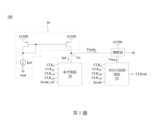
請參閱第1圖,第1圖為根據本揭示內容的一些實施例所繪示的一訊號轉換電路100的結構示意圖。訊號轉換電路100包含一相位內插器(phase interpolator)電路10以及一偏壓產生電路。於一些實施例中,如第1圖所示,所述偏壓產生電路包含一參考電路20、一電流鏡電路30(即,電流源)以及一穩壓器40。結構上,參考電路20與電流鏡電路30耦接於一節點N1,而穩壓器40又耦接於節點N1、一系統高電壓AVDD與相位內插器電路10之間。於一些實施例中,穩壓器40可為低壓差穩壓器(low-dropout regulator,LDO)。Please refer to FIG. 1 , which is a schematic structural diagram of a
於第1圖的實施例中,所述偏壓產生電路可透過穩壓器40提供一偏壓電壓Vbias至相位內插器電路10,而相位內插器電路10用以根據一數位訊號Scode將複數個輸入時脈訊號CLK0、CLK90、CLK180、CLK270轉換為一輸出時脈訊號CLKout。以下將參考第2圖詳細說明相位內插器電路10的結構與操作。In the embodiment of FIG. 1 , the bias generating circuit can provide a bias voltage Vbias to the
請參閱第2圖,第2圖為根據本揭示內容的一些實施例所繪示的相位內插器電路10的具體電路示意圖。於一些實施例中,如第2圖所示,相位內插器電路10包含並聯連接於偏壓電壓Vbias和一接地電壓Gnd之間的複數個電晶體對TP[1]~TP[n],其中n為大於1的正整數。於一些實施例中,多個電晶體對TP[1]~TP[n]分為複數組,且每組電晶體對用以接收多個輸入時脈訊號CLK0、CLK90、CLK180、CLK270中的一對應輸入時脈訊號。Please refer to FIG. 2 , which is a detailed circuit diagram of the
詳細而言,輸入時脈訊號CLK0代表具有0度相位的時脈訊號,輸入時脈訊號CLK90代表具有90度相位的時脈訊號,輸入時脈訊號CLK180代表具有180度相位的時脈訊號,而輸入時脈訊號CLK270代表具有270度相位的時脈訊號。換句話說,輸入至相位內插器電路10的多個輸入時脈訊號CLK0、CLK90、CLK180、CLK270的相位彼此不同。Specifically, the input clock signal CLK0 represents a clock signal with a phase of 0 degrees, the input clock signal CLK90 represents a clock signal with a phase of 90 degrees, and the input clock signal CLK180 represents a clock with a phase of 180 degrees. signal, and the input clock signal CLK270 represents a clock signal with a phase of 270 degrees. In other words, the phases of the plurality of input clock signals CLK0 , CLK90 , CLK180 , and CLK270 input to the
於一些實務應用中,相位內插器電路10包含32個電晶體對TP[1]~TP[32],且分為4組。換言之,多個電晶體對TP[1]~TP[8]為一組,多個電晶體對TP[9]~TP[16]為一組,多個電晶體對TP[17]~TP[24]為一組,而多個電晶體對TP[25]~TP[32]為一組。多個電晶體對TP[1]~TP[8]接收輸入時脈訊號CLK0,多個電晶體對TP[9]~TP[16]接收輸入時脈訊號CLK90,多個電晶體對TP[17]~TP[24]接收輸入時脈訊號CLK180,而多個電晶體對TP[25]~TP[32]接收輸入時脈訊號CLK270。In some practical applications, the
於一些實施例中,多個電晶體對TP[1]~TP[n]的結構彼此相同。以下將以電晶體對TP[1]為例說明電晶體對TP的結構。如第2圖所示,電晶體對TP[1]包含一第一電晶體T1、一第二電晶體T2、一第一開關ST1以及一第二開關ST2。第一電晶體T1的一第一端(例如:源極)接收偏壓電壓Vbias,第二電晶體T2的一第一端(例如:源極)接收接地電壓Gnd,第一電晶體T1的一控制端(例如:閘極)與第二電晶體T2的一控制端(例如:閘極)接收輸入時脈訊號CLK0(或者,多個輸入時脈訊號CLK0、CLK90、CLK180、CLK270中的一者)。第一開關ST1與第二開關ST2串聯連接後耦接於第一電晶體T1的一第二端(例如:汲極)與第二電晶體T2的一第二端(例如:汲極)之間。應當理解,第一電晶體T1可為P型金屬氧化物半導體場效電晶體,且第二電晶體T2可為N型金屬氧化物半導體場效電晶體。In some embodiments, the structures of the plurality of transistor pairs TP[1]~TP[n] are the same as each other. The following will take the transistor pair TP[1] as an example to illustrate the structure of the transistor pair TP. As shown in Figure 2, the transistor pair TP[1] includes a first transistor T1, a second transistor T2, a first switch ST1 and a second switch ST2. A first terminal (for example, source) of the first transistor T1 receives the bias voltage Vbias. A first terminal (for example, the source) of the second transistor T2 receives the ground voltage Gnd. A first terminal of the first transistor T1 The control terminal (for example: gate) and a control terminal (for example: gate) of the second transistor T2 receive the input clock signal CLK0 (or multiple input clock signals CLK0 , CLK90 , CLK180 , CLK one of270 ). The first switch ST1 and the second switch ST2 are connected in series and coupled between a second terminal (for example, the drain) of the first transistor T1 and a second terminal (for example, the drain) of the second transistor T2 . It should be understood that the first transistor T1 may be a P-type metal oxide semiconductor field effect transistor, and the second transistor T2 may be an N-type metal oxide semiconductor field effect transistor.
於一些實施例中,數位訊號Scode具有複數個位元,且數位訊號Scode的位元數量與多個電晶體對TP[1]~TP[n]的數量相同。多個電晶體對TP[1]~TP[n] 各自接收數位訊號Scode的多個位元中之一對應位元。舉例來說,電晶體對TP[1]接收數位訊號Scode的第1個位元,而電晶體對TP[2]接收數位訊號Scode的第2個位元。進一步地說,數位訊號Scode的每個位元具有一邏輯值。據此,電晶體對TP[1]中的第一開關ST1與第二開關ST2可根據數位訊號Scode的第1個位元的邏輯值(即,邏輯“0”或邏輯“1”)選擇性地導通。於第2圖的實施例中,電晶體對TP[1]中的第一開關ST1與第二開關ST2為同時導通或不導通。其餘電晶體對TP[2]~TP[n]中開關的操作可依此類推,故不在此贅述。In some embodiments, the digital signal Scode has a plurality of bits, and the number of bits of the digital signal Scode is the same as the number of transistor pairs TP[1]~TP[n]. The plurality of transistor pairs TP[1]~TP[n] each receive a corresponding bit among the plurality of bits of the digital signal Scode. For example, the transistor pair TP[1] receives the first bit of the digital signal Scode, and the transistor pair TP[2] receives the second bit of the digital signal Scode. Furthermore, each bit of the digital signal Scode has a logical value. Accordingly, the first switch ST1 and the second switch ST2 in the transistor pair TP[1] can be selective according to the logic value of the first bit of the digital signal Scode (ie, logic "0" or logic "1") ground conduction. In the embodiment of FIG. 2 , the first switch ST1 and the second switch ST2 in the transistor pair TP[1] are conductive or non-conductive at the same time. The operations of the switches in TP[2]~TP[n] by other transistors can be deduced in the same way, so they will not be described in detail here.
應當理解,數位訊號Scode可具有複數個位元組態,且多個位元組態分別表示數位訊號Scode的多個位元的不同組合。於一些實務應用中,數位訊號Scode為32位元,並由8個邏輯“1”以及24個邏輯“0”組成。舉例來說,於一時間點,數位訊號Scode的第1至8個位元為邏輯“1”,且數位訊號Scode的第9至32個位元為邏輯“0”,此即數位訊號Scode的其中一位元組態。數位訊號Scode的其餘位元組態可依此類推,故不在此贅述。It should be understood that the digital signal Scode may have a plurality of bit configurations, and the multiple bit configurations respectively represent different combinations of multiple bits of the digital signal Scode. In some practical applications, the digital signal Scode is 32 bits and consists of 8 logical "1"s and 24 logical "0"s. For example, at a point in time, the 1st to 8th bits of the digital signal Scode are logic "1", and the 9th to 32nd bits of the digital signal Scode are logic "0", which is the value of the digital signal Scode. One-bit configuration. The remaining bit configurations of the digital signal Scode can be deduced in this way, so they will not be described again here.
於一些實施例中,數位訊號Scode經操作者控制可具有特定位元組態(即,數位訊號Scode的多個位元組態中之一者)。相位內插器電路10中的多個電晶體對TP[1]~TP[n]則根據具有特定位元組態的數位訊號Scode對多個輸入時脈訊號CLK0、CLK90、CLK180、CLK270執行內插操作,以合成出輸出時脈訊號CLKout。理論上,相位內插器電路10根據數位訊號Scode所產生的輸出時脈訊號CLKout應具有與所述特定位元組態相對應的特定相位(即,操作者預設的相位)。換言之,不同位元組態的數位訊號Scode理應分別對應至不同相位的輸出時脈訊號CLKout。然而,相位內插器電路10在實務上時常因為製程變異而受到影響,導致輸出時脈訊號CLKout不具有操作者預設的相位。In some embodiments, the digital signal Scode may have a specific bit configuration (ie, one of multiple bit configurations of the digital signal Scode) under operator control. The plurality of transistor pairs TP[1]~TP[n] in the
值得注意的是,藉由使用所述偏壓產生電路所提供的偏壓電壓Vbias,相位內插器電路10因製程變異產生的誤差可獲得校正,使得相位內插器電路10所輸出的輸出時脈訊號CLKout可具有與數位訊號Scode的多個位元組態中之一者對應的一預設相位。應當理解,所述預設相位可為在0至360度之間的任意相位。以下將詳細說明如何產生偏壓電壓Vbias。It is worth noting that by using the bias voltage Vbias provided by the bias generating circuit, the error caused by the process variation of the
於一些實施例中,前述偏壓產生電路根據參考電路20所產生的一參考資訊(圖中未示)產生合適的偏壓電壓Vbias。於第1圖的實施例中,參考電路20為相位內插器電路10的複製電路,亦即,參考電路20的電路結構大致上與相位內插器電路10的電路結構相同。舉例來說,參考電路20包含並聯連接的複數個電晶體對(圖中未示)。為了反映相位內插器電路10因為製程變異而產生的變化,參考電路20的多個電晶體對亦按照相同於多個電晶體對TP[1]~TP[n]的分組方式分為複數組,以分別接收如第1圖所示的多個輸入時脈訊號CLK0、CLK90、CLK180、CLK270。In some embodiments, the aforementioned bias voltage generating circuit generates an appropriate bias voltage Vbias according to a reference information (not shown in the figure) generated by the
此外,參考電路20還接收類似於數位訊號Scode的一參考數位訊號Scode_ref。於一些實施例中,參考數位訊號Scode_ref的位元數量相同於數位訊號Scode的位元數量,但參考數位訊號Scode_ref經設定而僅具有一個固定的位元組態(即,預設位元組態)。參考數位訊號Scode_ref的預設位元組態可為前述數位訊號Scode的多個位元組態中之一者。應當理解,參考數位訊號Scode_ref的預設位元組態包含多個位元,而參考電路20的多個電晶體對各自接收參考數位訊號Scode_ref的多個位元中之一對應位元。In addition, the
如第1圖所示,參考電路20接收多個輸入時脈訊號CLK0、CLK90、CLK180、CLK270與參考數位訊號Scode_ref,但可以不輸出合成時脈訊號,因為參考電路20接收前述多個訊號僅是為了反映相位內插器電路10因為製程變異而產生的變化。此外,在接收參考數位訊號Scode_ref且不輸出合成時脈訊號的情況下,參考電路20的功耗亦可減少。As shown in Figure 1, the
應當理解,參考電路20可能因為製程變異而使內部電晶體的上升時間(rise time)或下降時間(fall time)較長或較短,因而又進一步影響了參考電路20的一等效電阻值的大小。於一些實施例中,參考電路20的等效電阻值包含以下成分:(1)製程變異所造成的電阻值誤差;以及(2)參考數位訊號Scode_ref的預設位元組態所設定的理想電阻值(亦即,理想電阻值為不考慮製程變異時,參考電路20中第一開關ST1與第二開關ST2導通的電晶體對所造成的電阻值)。前述參考資訊即為參考電路20因為製程變異而具有的等效電阻值。進一步地說,由於參考電路20與相位內插器電路10是以相同製程製造,參考電路20所提供的參考資訊關聯於相位內插器電路10因為製程變異而產生的變化。It should be understood that the
如第1圖所示,電流鏡電路30可根據一參考電流Iref產生一預設電流Ipd至參考電路20,以在節點N1產生一節點電壓Vnode。於第1圖的實施例中,節點電壓Vnode即為預設電流Ipd乘上參考電路20的等效電阻值。接著,穩壓器40可接收並穩定節點電壓Vnode,以產生偏壓電壓Vbias至相位內插器電路10。As shown in FIG. 1 , the
值得注意的是,由於參考電路20與相位內插器電路10是以相同製程製造,前述偏壓產生電路根據參考電路20的等效電阻值與預設電流Ipd所產生的偏壓電壓Vbias將具有能夠補償相位內插器電路10的製程變異的電壓大小。舉例來說,若相位內插器電路10(或/及參考電路20)因為製程變異而使內部電晶體的上升或下降時間較短,則參考電路20的等效電阻值相對較小。由於預設電流Ipd的大小固定,前述偏壓產生電路將依據較小的節點電壓Vnode產生較小的偏壓電壓Vbias至相位內插器電路10,以拉長相位內插器電路10內部電晶體的上升或下降時間。又例如,若相位內插器電路10(或/及參考電路20)因為製程變異而使內部電晶體的上升或下降時間較長,則參考電路20的等效電阻值相對較大。由於預設電流Ipd的大小固定,前述偏壓產生電路將依據較大的節點電壓Vnode產生較大的偏壓電壓Vbias至相位內插器電路10,以縮短相位內插器電路10內部電晶體的上升或下降時間。藉由校正相位內插器電路10的偏壓,相位內插器電路10可產生具有與數位訊號Scode的多個位元組態中之一者對應的預設相位的輸出時脈訊號CLKout。It is worth noting that since the
於前述實施例中,前述偏壓產生電路透過穩壓器40穩定節點電壓Vnode來產生偏壓電壓Vbias,但本揭示內容並不以此為限。由前述可知,節點電壓Vnode和偏壓電壓Vbias呈現正相關,因而於一些實施例中,穩壓器40可以省略且前述偏壓產生電路直接將節點電壓Vnode作為偏壓電壓Vbias輸出至相位內插器電路10。In the foregoing embodiments, the bias generating circuit generates the bias voltage Vbias by stabilizing the node voltage Vnode through the
於前述實施例中,第1圖中僅示出一個輸出時脈訊號CLKout,但本揭示內容並不以此為限。於其他實施例中,相位內插器電路10可產生彼此相差一特定相位(例如:180度相位、90度相位)的二個輸出時脈訊號。換言之,本揭示內容的相位內插器電路可產生至少一輸出時脈訊號。In the foregoing embodiments, only one output clock signal CLKout is shown in Figure 1, but the present disclosure is not limited thereto. In other embodiments, the
請參閱第3A及3B圖,第3A圖為根據本揭示內容的一些實施例所繪示偏壓未經校正的相位內插器電路10的實驗數據,而第3B圖為根據本揭示內容的一些實施例所繪示接收偏壓電壓 Vbias的相位內插器電路10的實驗數據。於第3A及3B圖中,橫軸的多個刻度分別表示數位訊號Scode的多個位元組態,而縱軸的多個刻度分別表示差分非線性度(differential nonlinearity,DNL)的大小。應當理解,差分非線性度愈小,則轉換電路的線性度愈高。因此,理想的轉換電路,其差分非線性度接近零。Please refer to Figures 3A and 3B. Figure 3A illustrates experimental data of a
如第3A圖所示,三條曲線FF(fast-fast)、TT(typical-typical)及SS(slow-slow)分別表示三種不同製程變異下的實驗數據,而縱軸範圍D則表示偏壓未經校正的相位內插器電路10的差分非線性度的大小分布。如第3B圖所示,三條曲線FF’、TT’及SS’分別表示三種不同製程變異下的實驗數據,而縱軸範圍D’則表示接收偏壓電壓 Vbias的相位內插器電路10的差分非線性度的大小分布。由第3A及3B圖可知,相較於偏壓未經校正的相位內插器電路10,接收偏壓電壓 Vbias的相位內插器電路10具有更佳的線性度。舉例來說,第3B圖中的縱軸範圍D’相較於第3A圖中的縱軸範圍D’減少了大約37%。As shown in Figure 3A, the three curves FF (fast-fast), TT (typical-typical) and SS (slow-slow) respectively represent the experimental data under three different process variations, while the vertical axis range D represents the bias voltage. Magnitude distribution of differential nonlinearity of the corrected
由上述本揭示內容的實施方式可知,藉由根據關聯於相位內插器電路因為製程變異而產生的變化的參考資訊來產生合適的偏壓電壓對相位內插器電路進行補償,本揭示內容的訊號轉換電路具有提高線性度的優勢。It can be seen from the above embodiments of the present disclosure that by generating appropriate bias voltages to compensate the phase interpolator circuit based on reference information associated with changes in the phase interpolator circuit due to process variations, the present disclosure The signal conversion circuit has the advantage of improving linearity.
雖然本揭示內容已以實施方式揭露如上,然其並非用以限定本揭示內容,所屬技術領域具有通常知識者在不脫離本揭示內容之精神和範圍內,當可作各種更動與潤飾,因此本揭示內容之保護範圍當視後附之申請專利範圍所界定者為準。Although the present disclosure has been disclosed in the above embodiments, it is not intended to limit the present disclosure. Those with ordinary skill in the technical field can make various modifications and modifications without departing from the spirit and scope of the present disclosure. Therefore, this disclosure The scope of protection of the disclosed content shall be determined by the scope of the patent application attached.
10:相位內插器電路10: Phase interpolator circuit
20:參考電路20:Reference circuit
30:電流鏡電路30: Current mirror circuit
40:穩壓器40: Voltage regulator
100:訊號轉換電路100: Signal conversion circuit
AVDD:系統高電壓AVDD: system high voltage
CLK0,CLK90,CLK180,CLK270:輸入時脈訊號CLK0 , CLK90 , CLK180 , CLK270 : Input clock signal
CLKout:輸出時脈訊號CLKout: output clock signal
Gnd:接地電壓Gnd: ground voltage
Ipd:預設電流Ipd: preset current
Iref:參考電流Iref: reference current
N1:節點N1: node
Scode:數位訊號Scode: digital signal
Scode_ref:參考數位訊號Scode_ref: reference digital signal
ST1:第一開關ST1: first switch
ST2:第二開關ST2: Second switch
T1:第一電晶體T1: the first transistor
T2:第二電晶體T2: Second transistor
TP[1]~TP[n]:電晶體對TP[1]~TP[n]: transistor pair
Vbias:偏壓電壓Vbias: bias voltage
Vnode:節點電壓Vnode: node voltage
FF,FF’,SS,SS’,TT,TT’:曲線FF,FF’,SS,SS’,TT,TT’:curve
D,D’:縱軸範圍D, D’: vertical axis range
第1圖係根據本揭示內容的一些實施例所繪示的訊號轉換電路的結構示意圖。 第2圖係根據本揭示內容的一些實施例所繪示的相位內插器電路的電路示意圖。 第3A圖係根據本揭示內容的一些實施例所繪示偏壓未經校正的相位內插器電路的實驗數據示意圖。 第3B圖係根據本揭示內容的一些實施例所繪示接收偏壓產生電路所提供的偏壓電壓的相位內插器電路的實驗數據示意圖。FIG. 1 is a schematic structural diagram of a signal conversion circuit according to some embodiments of the present disclosure. Figure 2 is a circuit schematic diagram of a phase interpolator circuit according to some embodiments of the present disclosure. Figure 3A is a schematic diagram of experimental data illustrating a phase interpolator circuit with uncorrected bias voltage according to some embodiments of the present disclosure. FIG. 3B is a schematic diagram of experimental data illustrating a phase interpolator circuit receiving a bias voltage provided by a bias generating circuit in accordance with some embodiments of the present disclosure.
國內寄存資訊(請依寄存機構、日期、號碼順序註記) 無 國外寄存資訊(請依寄存國家、機構、日期、號碼順序註記) 無Domestic storage information (please note in order of storage institution, date and number) without Overseas storage information (please note in order of storage country, institution, date, and number) without
10:相位內插器電路10: Phase interpolator circuit
20:參考電路20:Reference circuit
30:電流鏡電路30: Current mirror circuit
40:穩壓器40: Voltage regulator
100:訊號轉換電路100: Signal conversion circuit
AVDD:系統高電壓AVDD: system high voltage
CLK0,CLK90,CLK180,CLK270:輸入時脈訊號CLK0 , CLK90 , CLK180 , CLK270 : Input clock signal
CLKout:輸出時脈訊號CLKout: output clock signal
Gnd:接地電壓Gnd: ground voltage
Ipd:預設電流Ipd: preset current
Iref:參考電流Iref: reference current
N1:節點N1: node
Scode:數位訊號Scode: digital signal
Scode_ref:數位訊號Scode_ref:Digital signal
Vbias:偏壓電壓Vbias: bias voltage
Vnode:節點電壓Vnode: node voltage
Claims (9)
Translated fromChinesePriority Applications (2)
| Application Number | Priority Date | Filing Date | Title |
|---|---|---|---|
| TW111108668ATWI813197B (en) | 2022-03-09 | 2022-03-09 | Signal conversion circuit and bias voltage generating circuit thereof |
| US18/173,787US12334916B2 (en) | 2022-03-09 | 2023-02-24 | Signal converting circuit and bias voltage generation circuit thereof |
Applications Claiming Priority (1)
| Application Number | Priority Date | Filing Date | Title |
|---|---|---|---|
| TW111108668ATWI813197B (en) | 2022-03-09 | 2022-03-09 | Signal conversion circuit and bias voltage generating circuit thereof |
Publications (2)
| Publication Number | Publication Date |
|---|---|
| TWI813197Btrue TWI813197B (en) | 2023-08-21 |
| TW202337132A TW202337132A (en) | 2023-09-16 |
Family
ID=87931276
Family Applications (1)
| Application Number | Title | Priority Date | Filing Date |
|---|---|---|---|
| TW111108668ATWI813197B (en) | 2022-03-09 | 2022-03-09 | Signal conversion circuit and bias voltage generating circuit thereof |
Country Status (2)
| Country | Link |
|---|---|
| US (1) | US12334916B2 (en) |
| TW (1) | TWI813197B (en) |
Citations (7)
| Publication number | Priority date | Publication date | Assignee | Title |
|---|---|---|---|---|
| US20070222530A1 (en)* | 2006-03-07 | 2007-09-27 | Woogeun Rhee | Hybrid current-starved phase-interpolation circuit for voltage-controlled devices |
| US20130069701A1 (en)* | 2011-09-20 | 2013-03-21 | Sunplus Technology Co., Ltd. | Phase interpolation circuit |
| US20130088274A1 (en)* | 2011-10-09 | 2013-04-11 | Realtek Semiconductor Corp. | Phase interpolator, multi-phase interpolation device, interpolated clock generating method and multi-phase clock generating method |
| US20140125394A1 (en)* | 2012-11-08 | 2014-05-08 | Avago Technologies General Ip (Singapore) Pte. Ltd. | Phase interpolator having adaptively biased phase mixer |
| US20170026167A1 (en)* | 2014-09-04 | 2017-01-26 | Inphi Corporation | Phase interpolator |
| US20180013411A1 (en)* | 2016-07-06 | 2018-01-11 | Via Alliance Semiconductor Co., Ltd. | Interpolator |
| US20210143822A1 (en)* | 2019-11-08 | 2021-05-13 | Phison Electronics Corp. | Signal generation circuit, memory storage device and signal generation method |
Family Cites Families (1)
| Publication number | Priority date | Publication date | Assignee | Title |
|---|---|---|---|---|
| US20160191041A1 (en) | 2014-12-30 | 2016-06-30 | Shine C. Chung | Circuit and Method for Power-On Reset of an Integrated Circuit |
- 2022
- 2022-03-09TWTW111108668Apatent/TWI813197B/enactive
- 2023
- 2023-02-24USUS18/173,787patent/US12334916B2/enactiveActive
Patent Citations (7)
| Publication number | Priority date | Publication date | Assignee | Title |
|---|---|---|---|---|
| US20070222530A1 (en)* | 2006-03-07 | 2007-09-27 | Woogeun Rhee | Hybrid current-starved phase-interpolation circuit for voltage-controlled devices |
| US20130069701A1 (en)* | 2011-09-20 | 2013-03-21 | Sunplus Technology Co., Ltd. | Phase interpolation circuit |
| US20130088274A1 (en)* | 2011-10-09 | 2013-04-11 | Realtek Semiconductor Corp. | Phase interpolator, multi-phase interpolation device, interpolated clock generating method and multi-phase clock generating method |
| US20140125394A1 (en)* | 2012-11-08 | 2014-05-08 | Avago Technologies General Ip (Singapore) Pte. Ltd. | Phase interpolator having adaptively biased phase mixer |
| US20170026167A1 (en)* | 2014-09-04 | 2017-01-26 | Inphi Corporation | Phase interpolator |
| US20180013411A1 (en)* | 2016-07-06 | 2018-01-11 | Via Alliance Semiconductor Co., Ltd. | Interpolator |
| US20210143822A1 (en)* | 2019-11-08 | 2021-05-13 | Phison Electronics Corp. | Signal generation circuit, memory storage device and signal generation method |
Also Published As
| Publication number | Publication date |
|---|---|
| TW202337132A (en) | 2023-09-16 |
| US20230291398A1 (en) | 2023-09-14 |
| US12334916B2 (en) | 2025-06-17 |
Similar Documents
| Publication | Publication Date | Title |
|---|---|---|
| CN106656116B (en) | High linearity phase interpolator | |
| US20090179674A1 (en) | Phase-combining circuit and timing signal generator circuit for carrying out a high-speed signal transmission | |
| US20050057379A1 (en) | A/D converter calibration | |
| CN105071809B (en) | Complementary current circuit, on-off circuit and the current mode digital-to-analog converter of Background calibration | |
| US20220239288A1 (en) | Gated tri-state inverter, and low power reduced area phase interpolator system including same, and method of operating same | |
| JP2010171781A (en) | Impedance adjustment circuit | |
| CN208369563U (en) | Digital analog converter | |
| TW202011698A (en) | Successive approximation register analog-to-digital converter and control circuit thereof | |
| US20100164765A1 (en) | DAC calibration circuits and methods | |
| TW201419766A (en) | Successive approximation analog-to-digital converter | |
| TWI813197B (en) | Signal conversion circuit and bias voltage generating circuit thereof | |
| CN104935321B (en) | Input/output impedance correction circuit and method | |
| TW202318804A (en) | Phase interpolator and phase buffer circuit | |
| CN107346959A (en) | A kind of operational amplifier that offset voltage correction is carried out for output services point | |
| CN116795169A (en) | Signal conversion circuit and bias voltage generation circuit thereof | |
| TWI792939B (en) | Signal conversion circuit | |
| CN106856405A (en) | A kind of switching current device and the digital analog converter based on the device | |
| CN117081570A (en) | On-chip resistor calibration circuit | |
| CN116527020A (en) | Duty cycle calibration circuit and method | |
| US6940331B2 (en) | Delayed tap signal generating circuit for controlling delay by interpolating two input clocks | |
| CN116195188A (en) | Phase shifter, method of using same and antenna system | |
| CN107437937B (en) | Working cycle generating device and working cycle generating method | |
| CN105049053A (en) | Complementary current circuit, switch circuit and current digital-to-analog converter of foreground correction | |
| CN108429540B (en) | A Low Power High Resolution Digital Phase Generator | |
| CN106330143B (en) | Duty-ratio calibrating circuit |