TWI811990B - Semiconductor structure and method for forming the same - Google Patents
Semiconductor structure and method for forming the sameDownload PDFInfo
- Publication number
- TWI811990B TWI811990BTW111104263ATW111104263ATWI811990BTW I811990 BTWI811990 BTW I811990BTW 111104263 ATW111104263 ATW 111104263ATW 111104263 ATW111104263 ATW 111104263ATW I811990 BTWI811990 BTW I811990B
- Authority
- TW
- Taiwan
- Prior art keywords
- thermal interface
- interface material
- die
- material film
- substrate
- Prior art date
Links
Images


Classifications
- H—ELECTRICITY
- H01—ELECTRIC ELEMENTS
- H01L—SEMICONDUCTOR DEVICES NOT COVERED BY CLASS H10
- H01L23/00—Details of semiconductor or other solid state devices
- H01L23/34—Arrangements for cooling, heating, ventilating or temperature compensation ; Temperature sensing arrangements
- H01L23/36—Selection of materials, or shaping, to facilitate cooling or heating, e.g. heatsinks
- H01L23/373—Cooling facilitated by selection of materials for the device or materials for thermal expansion adaptation, e.g. carbon
- H01L23/3735—Laminates or multilayers, e.g. direct bond copper ceramic substrates
- H—ELECTRICITY
- H01—ELECTRIC ELEMENTS
- H01L—SEMICONDUCTOR DEVICES NOT COVERED BY CLASS H10
- H01L23/00—Details of semiconductor or other solid state devices
- H01L23/34—Arrangements for cooling, heating, ventilating or temperature compensation ; Temperature sensing arrangements
- H01L23/36—Selection of materials, or shaping, to facilitate cooling or heating, e.g. heatsinks
- H01L23/367—Cooling facilitated by shape of device
- H01L23/3672—Foil-like cooling fins or heat sinks
- H—ELECTRICITY
- H01—ELECTRIC ELEMENTS
- H01L—SEMICONDUCTOR DEVICES NOT COVERED BY CLASS H10
- H01L23/00—Details of semiconductor or other solid state devices
- H01L23/52—Arrangements for conducting electric current within the device in operation from one component to another, i.e. interconnections, e.g. wires, lead frames
- H01L23/538—Arrangements for conducting electric current within the device in operation from one component to another, i.e. interconnections, e.g. wires, lead frames the interconnection structure between a plurality of semiconductor chips being formed on, or in, insulating substrates
- H01L23/5384—Conductive vias through the substrate with or without pins, e.g. buried coaxial conductors
- H—ELECTRICITY
- H01—ELECTRIC ELEMENTS
- H01L—SEMICONDUCTOR DEVICES NOT COVERED BY CLASS H10
- H01L23/00—Details of semiconductor or other solid state devices
- H01L23/34—Arrangements for cooling, heating, ventilating or temperature compensation ; Temperature sensing arrangements
- H01L23/36—Selection of materials, or shaping, to facilitate cooling or heating, e.g. heatsinks
- H01L23/367—Cooling facilitated by shape of device
- H01L23/3675—Cooling facilitated by shape of device characterised by the shape of the housing
- H—ELECTRICITY
- H01—ELECTRIC ELEMENTS
- H01L—SEMICONDUCTOR DEVICES NOT COVERED BY CLASS H10
- H01L21/00—Processes or apparatus adapted for the manufacture or treatment of semiconductor or solid state devices or of parts thereof
- H01L21/02—Manufacture or treatment of semiconductor devices or of parts thereof
- H01L21/04—Manufacture or treatment of semiconductor devices or of parts thereof the devices having potential barriers, e.g. a PN junction, depletion layer or carrier concentration layer
- H01L21/50—Assembly of semiconductor devices using processes or apparatus not provided for in a single one of the groups H01L21/18 - H01L21/326 or H10D48/04 - H10D48/07 e.g. sealing of a cap to a base of a container
- H01L21/52—Mounting semiconductor bodies in containers
- H—ELECTRICITY
- H01—ELECTRIC ELEMENTS
- H01L—SEMICONDUCTOR DEVICES NOT COVERED BY CLASS H10
- H01L23/00—Details of semiconductor or other solid state devices
- H01L23/02—Containers; Seals
- H01L23/04—Containers; Seals characterised by the shape of the container or parts, e.g. caps, walls
- H—ELECTRICITY
- H01—ELECTRIC ELEMENTS
- H01L—SEMICONDUCTOR DEVICES NOT COVERED BY CLASS H10
- H01L23/00—Details of semiconductor or other solid state devices
- H01L23/16—Fillings or auxiliary members in containers or encapsulations, e.g. centering rings
- H—ELECTRICITY
- H01—ELECTRIC ELEMENTS
- H01L—SEMICONDUCTOR DEVICES NOT COVERED BY CLASS H10
- H01L23/00—Details of semiconductor or other solid state devices
- H01L23/28—Encapsulations, e.g. encapsulating layers, coatings, e.g. for protection
- H01L23/31—Encapsulations, e.g. encapsulating layers, coatings, e.g. for protection characterised by the arrangement or shape
- H01L23/3107—Encapsulations, e.g. encapsulating layers, coatings, e.g. for protection characterised by the arrangement or shape the device being completely enclosed
- H01L23/3121—Encapsulations, e.g. encapsulating layers, coatings, e.g. for protection characterised by the arrangement or shape the device being completely enclosed a substrate forming part of the encapsulation
- H01L23/3128—Encapsulations, e.g. encapsulating layers, coatings, e.g. for protection characterised by the arrangement or shape the device being completely enclosed a substrate forming part of the encapsulation the substrate having spherical bumps for external connection
- H—ELECTRICITY
- H01—ELECTRIC ELEMENTS
- H01L—SEMICONDUCTOR DEVICES NOT COVERED BY CLASS H10
- H01L23/00—Details of semiconductor or other solid state devices
- H01L23/28—Encapsulations, e.g. encapsulating layers, coatings, e.g. for protection
- H01L23/31—Encapsulations, e.g. encapsulating layers, coatings, e.g. for protection characterised by the arrangement or shape
- H01L23/3107—Encapsulations, e.g. encapsulating layers, coatings, e.g. for protection characterised by the arrangement or shape the device being completely enclosed
- H01L23/3135—Double encapsulation or coating and encapsulation
- H—ELECTRICITY
- H01—ELECTRIC ELEMENTS
- H01L—SEMICONDUCTOR DEVICES NOT COVERED BY CLASS H10
- H01L23/00—Details of semiconductor or other solid state devices
- H01L23/34—Arrangements for cooling, heating, ventilating or temperature compensation ; Temperature sensing arrangements
- H01L23/36—Selection of materials, or shaping, to facilitate cooling or heating, e.g. heatsinks
- H01L23/373—Cooling facilitated by selection of materials for the device or materials for thermal expansion adaptation, e.g. carbon
- H—ELECTRICITY
- H01—ELECTRIC ELEMENTS
- H01L—SEMICONDUCTOR DEVICES NOT COVERED BY CLASS H10
- H01L23/00—Details of semiconductor or other solid state devices
- H01L23/48—Arrangements for conducting electric current to or from the solid state body in operation, e.g. leads, terminal arrangements ; Selection of materials therefor
- H01L23/488—Arrangements for conducting electric current to or from the solid state body in operation, e.g. leads, terminal arrangements ; Selection of materials therefor consisting of soldered or bonded constructions
- H01L23/498—Leads, i.e. metallisations or lead-frames on insulating substrates, e.g. chip carriers
- H01L23/49822—Multilayer substrates
- H—ELECTRICITY
- H01—ELECTRIC ELEMENTS
- H01L—SEMICONDUCTOR DEVICES NOT COVERED BY CLASS H10
- H01L23/00—Details of semiconductor or other solid state devices
- H01L23/48—Arrangements for conducting electric current to or from the solid state body in operation, e.g. leads, terminal arrangements ; Selection of materials therefor
- H01L23/488—Arrangements for conducting electric current to or from the solid state body in operation, e.g. leads, terminal arrangements ; Selection of materials therefor consisting of soldered or bonded constructions
- H01L23/498—Leads, i.e. metallisations or lead-frames on insulating substrates, e.g. chip carriers
- H01L23/49833—Leads, i.e. metallisations or lead-frames on insulating substrates, e.g. chip carriers the chip support structure consisting of a plurality of insulating substrates
- H—ELECTRICITY
- H01—ELECTRIC ELEMENTS
- H01L—SEMICONDUCTOR DEVICES NOT COVERED BY CLASS H10
- H01L23/00—Details of semiconductor or other solid state devices
- H01L23/48—Arrangements for conducting electric current to or from the solid state body in operation, e.g. leads, terminal arrangements ; Selection of materials therefor
- H01L23/488—Arrangements for conducting electric current to or from the solid state body in operation, e.g. leads, terminal arrangements ; Selection of materials therefor consisting of soldered or bonded constructions
- H01L23/498—Leads, i.e. metallisations or lead-frames on insulating substrates, e.g. chip carriers
- H01L23/49838—Geometry or layout
- H—ELECTRICITY
- H01—ELECTRIC ELEMENTS
- H01L—SEMICONDUCTOR DEVICES NOT COVERED BY CLASS H10
- H01L24/00—Arrangements for connecting or disconnecting semiconductor or solid-state bodies; Methods or apparatus related thereto
- H01L24/01—Means for bonding being attached to, or being formed on, the surface to be connected, e.g. chip-to-package, die-attach, "first-level" interconnects; Manufacturing methods related thereto
- H01L24/26—Layer connectors, e.g. plate connectors, solder or adhesive layers; Manufacturing methods related thereto
- H01L24/28—Structure, shape, material or disposition of the layer connectors prior to the connecting process
- H01L24/29—Structure, shape, material or disposition of the layer connectors prior to the connecting process of an individual layer connector
- H—ELECTRICITY
- H01—ELECTRIC ELEMENTS
- H01L—SEMICONDUCTOR DEVICES NOT COVERED BY CLASS H10
- H01L24/00—Arrangements for connecting or disconnecting semiconductor or solid-state bodies; Methods or apparatus related thereto
- H01L24/01—Means for bonding being attached to, or being formed on, the surface to be connected, e.g. chip-to-package, die-attach, "first-level" interconnects; Manufacturing methods related thereto
- H01L24/26—Layer connectors, e.g. plate connectors, solder or adhesive layers; Manufacturing methods related thereto
- H01L24/31—Structure, shape, material or disposition of the layer connectors after the connecting process
- H01L24/32—Structure, shape, material or disposition of the layer connectors after the connecting process of an individual layer connector
- H—ELECTRICITY
- H01—ELECTRIC ELEMENTS
- H01L—SEMICONDUCTOR DEVICES NOT COVERED BY CLASS H10
- H01L24/00—Arrangements for connecting or disconnecting semiconductor or solid-state bodies; Methods or apparatus related thereto
- H01L24/80—Methods for connecting semiconductor or other solid state bodies using means for bonding being attached to, or being formed on, the surface to be connected
- H01L24/83—Methods for connecting semiconductor or other solid state bodies using means for bonding being attached to, or being formed on, the surface to be connected using a layer connector
- H—ELECTRICITY
- H01—ELECTRIC ELEMENTS
- H01L—SEMICONDUCTOR DEVICES NOT COVERED BY CLASS H10
- H01L24/00—Arrangements for connecting or disconnecting semiconductor or solid-state bodies; Methods or apparatus related thereto
- H01L24/93—Batch processes
- H01L24/95—Batch processes at chip-level, i.e. with connecting carried out on a plurality of singulated devices, i.e. on diced chips
- H01L24/97—Batch processes at chip-level, i.e. with connecting carried out on a plurality of singulated devices, i.e. on diced chips the devices being connected to a common substrate, e.g. interposer, said common substrate being separable into individual assemblies after connecting
- H—ELECTRICITY
- H01—ELECTRIC ELEMENTS
- H01L—SEMICONDUCTOR DEVICES NOT COVERED BY CLASS H10
- H01L25/00—Assemblies consisting of a plurality of semiconductor or other solid state devices
- H01L25/03—Assemblies consisting of a plurality of semiconductor or other solid state devices all the devices being of a type provided for in a single subclass of subclasses H10B, H10D, H10F, H10H, H10K or H10N, e.g. assemblies of rectifier diodes
- H01L25/04—Assemblies consisting of a plurality of semiconductor or other solid state devices all the devices being of a type provided for in a single subclass of subclasses H10B, H10D, H10F, H10H, H10K or H10N, e.g. assemblies of rectifier diodes the devices not having separate containers
- H01L25/065—Assemblies consisting of a plurality of semiconductor or other solid state devices all the devices being of a type provided for in a single subclass of subclasses H10B, H10D, H10F, H10H, H10K or H10N, e.g. assemblies of rectifier diodes the devices not having separate containers the devices being of a type provided for in group H10D89/00
- H01L25/0655—Assemblies consisting of a plurality of semiconductor or other solid state devices all the devices being of a type provided for in a single subclass of subclasses H10B, H10D, H10F, H10H, H10K or H10N, e.g. assemblies of rectifier diodes the devices not having separate containers the devices being of a type provided for in group H10D89/00 the devices being arranged next to each other
- H—ELECTRICITY
- H01—ELECTRIC ELEMENTS
- H01L—SEMICONDUCTOR DEVICES NOT COVERED BY CLASS H10
- H01L25/00—Assemblies consisting of a plurality of semiconductor or other solid state devices
- H01L25/03—Assemblies consisting of a plurality of semiconductor or other solid state devices all the devices being of a type provided for in a single subclass of subclasses H10B, H10D, H10F, H10H, H10K or H10N, e.g. assemblies of rectifier diodes
- H01L25/04—Assemblies consisting of a plurality of semiconductor or other solid state devices all the devices being of a type provided for in a single subclass of subclasses H10B, H10D, H10F, H10H, H10K or H10N, e.g. assemblies of rectifier diodes the devices not having separate containers
- H01L25/07—Assemblies consisting of a plurality of semiconductor or other solid state devices all the devices being of a type provided for in a single subclass of subclasses H10B, H10D, H10F, H10H, H10K or H10N, e.g. assemblies of rectifier diodes the devices not having separate containers the devices being of a type provided for in group subclass H10D
- H01L25/072—Assemblies consisting of a plurality of semiconductor or other solid state devices all the devices being of a type provided for in a single subclass of subclasses H10B, H10D, H10F, H10H, H10K or H10N, e.g. assemblies of rectifier diodes the devices not having separate containers the devices being of a type provided for in group subclass H10D the devices being arranged next to each other
- H—ELECTRICITY
- H01—ELECTRIC ELEMENTS
- H01L—SEMICONDUCTOR DEVICES NOT COVERED BY CLASS H10
- H01L25/00—Assemblies consisting of a plurality of semiconductor or other solid state devices
- H01L25/18—Assemblies consisting of a plurality of semiconductor or other solid state devices the devices being of the types provided for in two or more different main groups of the same subclass of H10B, H10D, H10F, H10H, H10K or H10N
- H—ELECTRICITY
- H01—ELECTRIC ELEMENTS
- H01L—SEMICONDUCTOR DEVICES NOT COVERED BY CLASS H10
- H01L25/00—Assemblies consisting of a plurality of semiconductor or other solid state devices
- H01L25/50—Multistep manufacturing processes of assemblies consisting of devices, the devices being individual devices of subclass H10D or integrated devices of class H10
- H—ELECTRICITY
- H01—ELECTRIC ELEMENTS
- H01L—SEMICONDUCTOR DEVICES NOT COVERED BY CLASS H10
- H01L2224/00—Indexing scheme for arrangements for connecting or disconnecting semiconductor or solid-state bodies and methods related thereto as covered by H01L24/00
- H01L2224/01—Means for bonding being attached to, or being formed on, the surface to be connected, e.g. chip-to-package, die-attach, "first-level" interconnects; Manufacturing methods related thereto
- H01L2224/10—Bump connectors; Manufacturing methods related thereto
- H01L2224/12—Structure, shape, material or disposition of the bump connectors prior to the connecting process
- H01L2224/13—Structure, shape, material or disposition of the bump connectors prior to the connecting process of an individual bump connector
- H01L2224/13001—Core members of the bump connector
- H01L2224/13099—Material
- H01L2224/131—Material with a principal constituent of the material being a metal or a metalloid, e.g. boron [B], silicon [Si], germanium [Ge], arsenic [As], antimony [Sb], tellurium [Te] and polonium [Po], and alloys thereof
- H01L2224/13101—Material with a principal constituent of the material being a metal or a metalloid, e.g. boron [B], silicon [Si], germanium [Ge], arsenic [As], antimony [Sb], tellurium [Te] and polonium [Po], and alloys thereof the principal constituent melting at a temperature of less than 400°C
- H—ELECTRICITY
- H01—ELECTRIC ELEMENTS
- H01L—SEMICONDUCTOR DEVICES NOT COVERED BY CLASS H10
- H01L2224/00—Indexing scheme for arrangements for connecting or disconnecting semiconductor or solid-state bodies and methods related thereto as covered by H01L24/00
- H01L2224/01—Means for bonding being attached to, or being formed on, the surface to be connected, e.g. chip-to-package, die-attach, "first-level" interconnects; Manufacturing methods related thereto
- H01L2224/10—Bump connectors; Manufacturing methods related thereto
- H01L2224/15—Structure, shape, material or disposition of the bump connectors after the connecting process
- H01L2224/16—Structure, shape, material or disposition of the bump connectors after the connecting process of an individual bump connector
- H01L2224/161—Disposition
- H01L2224/16151—Disposition the bump connector connecting between a semiconductor or solid-state body and an item not being a semiconductor or solid-state body, e.g. chip-to-substrate, chip-to-passive
- H01L2224/16221—Disposition the bump connector connecting between a semiconductor or solid-state body and an item not being a semiconductor or solid-state body, e.g. chip-to-substrate, chip-to-passive the body and the item being stacked
- H01L2224/16225—Disposition the bump connector connecting between a semiconductor or solid-state body and an item not being a semiconductor or solid-state body, e.g. chip-to-substrate, chip-to-passive the body and the item being stacked the item being non-metallic, e.g. insulating substrate with or without metallisation
- H01L2224/16227—Disposition the bump connector connecting between a semiconductor or solid-state body and an item not being a semiconductor or solid-state body, e.g. chip-to-substrate, chip-to-passive the body and the item being stacked the item being non-metallic, e.g. insulating substrate with or without metallisation the bump connector connecting to a bond pad of the item
- H—ELECTRICITY
- H01—ELECTRIC ELEMENTS
- H01L—SEMICONDUCTOR DEVICES NOT COVERED BY CLASS H10
- H01L2224/00—Indexing scheme for arrangements for connecting or disconnecting semiconductor or solid-state bodies and methods related thereto as covered by H01L24/00
- H01L2224/01—Means for bonding being attached to, or being formed on, the surface to be connected, e.g. chip-to-package, die-attach, "first-level" interconnects; Manufacturing methods related thereto
- H01L2224/10—Bump connectors; Manufacturing methods related thereto
- H01L2224/15—Structure, shape, material or disposition of the bump connectors after the connecting process
- H01L2224/16—Structure, shape, material or disposition of the bump connectors after the connecting process of an individual bump connector
- H01L2224/161—Disposition
- H01L2224/16151—Disposition the bump connector connecting between a semiconductor or solid-state body and an item not being a semiconductor or solid-state body, e.g. chip-to-substrate, chip-to-passive
- H01L2224/16221—Disposition the bump connector connecting between a semiconductor or solid-state body and an item not being a semiconductor or solid-state body, e.g. chip-to-substrate, chip-to-passive the body and the item being stacked
- H01L2224/16225—Disposition the bump connector connecting between a semiconductor or solid-state body and an item not being a semiconductor or solid-state body, e.g. chip-to-substrate, chip-to-passive the body and the item being stacked the item being non-metallic, e.g. insulating substrate with or without metallisation
- H01L2224/16238—Disposition the bump connector connecting between a semiconductor or solid-state body and an item not being a semiconductor or solid-state body, e.g. chip-to-substrate, chip-to-passive the body and the item being stacked the item being non-metallic, e.g. insulating substrate with or without metallisation the bump connector connecting to a bonding area protruding from the surface of the item
- H—ELECTRICITY
- H01—ELECTRIC ELEMENTS
- H01L—SEMICONDUCTOR DEVICES NOT COVERED BY CLASS H10
- H01L2224/00—Indexing scheme for arrangements for connecting or disconnecting semiconductor or solid-state bodies and methods related thereto as covered by H01L24/00
- H01L2224/01—Means for bonding being attached to, or being formed on, the surface to be connected, e.g. chip-to-package, die-attach, "first-level" interconnects; Manufacturing methods related thereto
- H01L2224/26—Layer connectors, e.g. plate connectors, solder or adhesive layers; Manufacturing methods related thereto
- H01L2224/31—Structure, shape, material or disposition of the layer connectors after the connecting process
- H01L2224/32—Structure, shape, material or disposition of the layer connectors after the connecting process of an individual layer connector
- H01L2224/321—Disposition
- H01L2224/32151—Disposition the layer connector connecting between a semiconductor or solid-state body and an item not being a semiconductor or solid-state body, e.g. chip-to-substrate, chip-to-passive
- H01L2224/32221—Disposition the layer connector connecting between a semiconductor or solid-state body and an item not being a semiconductor or solid-state body, e.g. chip-to-substrate, chip-to-passive the body and the item being stacked
- H01L2224/32225—Disposition the layer connector connecting between a semiconductor or solid-state body and an item not being a semiconductor or solid-state body, e.g. chip-to-substrate, chip-to-passive the body and the item being stacked the item being non-metallic, e.g. insulating substrate with or without metallisation
- H—ELECTRICITY
- H01—ELECTRIC ELEMENTS
- H01L—SEMICONDUCTOR DEVICES NOT COVERED BY CLASS H10
- H01L2224/00—Indexing scheme for arrangements for connecting or disconnecting semiconductor or solid-state bodies and methods related thereto as covered by H01L24/00
- H01L2224/01—Means for bonding being attached to, or being formed on, the surface to be connected, e.g. chip-to-package, die-attach, "first-level" interconnects; Manufacturing methods related thereto
- H01L2224/26—Layer connectors, e.g. plate connectors, solder or adhesive layers; Manufacturing methods related thereto
- H01L2224/31—Structure, shape, material or disposition of the layer connectors after the connecting process
- H01L2224/32—Structure, shape, material or disposition of the layer connectors after the connecting process of an individual layer connector
- H01L2224/321—Disposition
- H01L2224/32151—Disposition the layer connector connecting between a semiconductor or solid-state body and an item not being a semiconductor or solid-state body, e.g. chip-to-substrate, chip-to-passive
- H01L2224/32221—Disposition the layer connector connecting between a semiconductor or solid-state body and an item not being a semiconductor or solid-state body, e.g. chip-to-substrate, chip-to-passive the body and the item being stacked
- H01L2224/32245—Disposition the layer connector connecting between a semiconductor or solid-state body and an item not being a semiconductor or solid-state body, e.g. chip-to-substrate, chip-to-passive the body and the item being stacked the item being metallic
- H—ELECTRICITY
- H01—ELECTRIC ELEMENTS
- H01L—SEMICONDUCTOR DEVICES NOT COVERED BY CLASS H10
- H01L2224/00—Indexing scheme for arrangements for connecting or disconnecting semiconductor or solid-state bodies and methods related thereto as covered by H01L24/00
- H01L2224/73—Means for bonding being of different types provided for in two or more of groups H01L2224/10, H01L2224/18, H01L2224/26, H01L2224/34, H01L2224/42, H01L2224/50, H01L2224/63, H01L2224/71
- H01L2224/732—Location after the connecting process
- H01L2224/73201—Location after the connecting process on the same surface
- H01L2224/73203—Bump and layer connectors
- H01L2224/73204—Bump and layer connectors the bump connector being embedded into the layer connector
- H—ELECTRICITY
- H01—ELECTRIC ELEMENTS
- H01L—SEMICONDUCTOR DEVICES NOT COVERED BY CLASS H10
- H01L2224/00—Indexing scheme for arrangements for connecting or disconnecting semiconductor or solid-state bodies and methods related thereto as covered by H01L24/00
- H01L2224/73—Means for bonding being of different types provided for in two or more of groups H01L2224/10, H01L2224/18, H01L2224/26, H01L2224/34, H01L2224/42, H01L2224/50, H01L2224/63, H01L2224/71
- H01L2224/732—Location after the connecting process
- H01L2224/73251—Location after the connecting process on different surfaces
- H01L2224/73253—Bump and layer connectors
- H—ELECTRICITY
- H01—ELECTRIC ELEMENTS
- H01L—SEMICONDUCTOR DEVICES NOT COVERED BY CLASS H10
- H01L2224/00—Indexing scheme for arrangements for connecting or disconnecting semiconductor or solid-state bodies and methods related thereto as covered by H01L24/00
- H01L2224/80—Methods for connecting semiconductor or other solid state bodies using means for bonding being attached to, or being formed on, the surface to be connected
- H01L2224/81—Methods for connecting semiconductor or other solid state bodies using means for bonding being attached to, or being formed on, the surface to be connected using a bump connector
- H01L2224/818—Bonding techniques
- H01L2224/81801—Soldering or alloying
- H01L2224/81815—Reflow soldering
- H—ELECTRICITY
- H01—ELECTRIC ELEMENTS
- H01L—SEMICONDUCTOR DEVICES NOT COVERED BY CLASS H10
- H01L2224/00—Indexing scheme for arrangements for connecting or disconnecting semiconductor or solid-state bodies and methods related thereto as covered by H01L24/00
- H01L2224/93—Batch processes
- H01L2224/95—Batch processes at chip-level, i.e. with connecting carried out on a plurality of singulated devices, i.e. on diced chips
- H01L2224/97—Batch processes at chip-level, i.e. with connecting carried out on a plurality of singulated devices, i.e. on diced chips the devices being connected to a common substrate, e.g. interposer, said common substrate being separable into individual assemblies after connecting
- H—ELECTRICITY
- H01—ELECTRIC ELEMENTS
- H01L—SEMICONDUCTOR DEVICES NOT COVERED BY CLASS H10
- H01L2225/00—Details relating to assemblies covered by the group H01L25/00 but not provided for in its subgroups
- H01L2225/03—All the devices being of a type provided for in the same main group of the same subclass of class H10, e.g. assemblies of rectifier diodes
- H01L2225/04—All the devices being of a type provided for in the same main group of the same subclass of class H10, e.g. assemblies of rectifier diodes the devices not having separate containers
- H01L2225/065—All the devices being of a type provided for in the same main group of the same subclass of class H10
- H01L2225/06503—Stacked arrangements of devices
- H01L2225/06589—Thermal management, e.g. cooling
- H—ELECTRICITY
- H01—ELECTRIC ELEMENTS
- H01L—SEMICONDUCTOR DEVICES NOT COVERED BY CLASS H10
- H01L23/00—Details of semiconductor or other solid state devices
- H01L23/34—Arrangements for cooling, heating, ventilating or temperature compensation ; Temperature sensing arrangements
- H01L23/36—Selection of materials, or shaping, to facilitate cooling or heating, e.g. heatsinks
- H01L23/373—Cooling facilitated by selection of materials for the device or materials for thermal expansion adaptation, e.g. carbon
- H01L23/3737—Organic materials with or without a thermoconductive filler
- H—ELECTRICITY
- H01—ELECTRIC ELEMENTS
- H01L—SEMICONDUCTOR DEVICES NOT COVERED BY CLASS H10
- H01L23/00—Details of semiconductor or other solid state devices
- H01L23/34—Arrangements for cooling, heating, ventilating or temperature compensation ; Temperature sensing arrangements
- H01L23/42—Fillings or auxiliary members in containers or encapsulations selected or arranged to facilitate heating or cooling
- H—ELECTRICITY
- H01—ELECTRIC ELEMENTS
- H01L—SEMICONDUCTOR DEVICES NOT COVERED BY CLASS H10
- H01L23/00—Details of semiconductor or other solid state devices
- H01L23/48—Arrangements for conducting electric current to or from the solid state body in operation, e.g. leads, terminal arrangements ; Selection of materials therefor
- H01L23/488—Arrangements for conducting electric current to or from the solid state body in operation, e.g. leads, terminal arrangements ; Selection of materials therefor consisting of soldered or bonded constructions
- H01L23/498—Leads, i.e. metallisations or lead-frames on insulating substrates, e.g. chip carriers
- H01L23/49811—Additional leads joined to the metallisation on the insulating substrate, e.g. pins, bumps, wires, flat leads
- H01L23/49816—Spherical bumps on the substrate for external connection, e.g. ball grid arrays [BGA]
- H—ELECTRICITY
- H01—ELECTRIC ELEMENTS
- H01L—SEMICONDUCTOR DEVICES NOT COVERED BY CLASS H10
- H01L23/00—Details of semiconductor or other solid state devices
- H01L23/552—Protection against radiation, e.g. light or electromagnetic waves
- H—ELECTRICITY
- H01—ELECTRIC ELEMENTS
- H01L—SEMICONDUCTOR DEVICES NOT COVERED BY CLASS H10
- H01L24/00—Arrangements for connecting or disconnecting semiconductor or solid-state bodies; Methods or apparatus related thereto
- H01L24/01—Means for bonding being attached to, or being formed on, the surface to be connected, e.g. chip-to-package, die-attach, "first-level" interconnects; Manufacturing methods related thereto
- H01L24/10—Bump connectors ; Manufacturing methods related thereto
- H01L24/12—Structure, shape, material or disposition of the bump connectors prior to the connecting process
- H01L24/13—Structure, shape, material or disposition of the bump connectors prior to the connecting process of an individual bump connector
- H—ELECTRICITY
- H01—ELECTRIC ELEMENTS
- H01L—SEMICONDUCTOR DEVICES NOT COVERED BY CLASS H10
- H01L24/00—Arrangements for connecting or disconnecting semiconductor or solid-state bodies; Methods or apparatus related thereto
- H01L24/01—Means for bonding being attached to, or being formed on, the surface to be connected, e.g. chip-to-package, die-attach, "first-level" interconnects; Manufacturing methods related thereto
- H01L24/10—Bump connectors ; Manufacturing methods related thereto
- H01L24/15—Structure, shape, material or disposition of the bump connectors after the connecting process
- H01L24/16—Structure, shape, material or disposition of the bump connectors after the connecting process of an individual bump connector
- H—ELECTRICITY
- H01—ELECTRIC ELEMENTS
- H01L—SEMICONDUCTOR DEVICES NOT COVERED BY CLASS H10
- H01L24/00—Arrangements for connecting or disconnecting semiconductor or solid-state bodies; Methods or apparatus related thereto
- H01L24/73—Means for bonding being of different types provided for in two or more of groups H01L24/10, H01L24/18, H01L24/26, H01L24/34, H01L24/42, H01L24/50, H01L24/63, H01L24/71
- H—ELECTRICITY
- H01—ELECTRIC ELEMENTS
- H01L—SEMICONDUCTOR DEVICES NOT COVERED BY CLASS H10
- H01L24/00—Arrangements for connecting or disconnecting semiconductor or solid-state bodies; Methods or apparatus related thereto
- H01L24/80—Methods for connecting semiconductor or other solid state bodies using means for bonding being attached to, or being formed on, the surface to be connected
- H01L24/81—Methods for connecting semiconductor or other solid state bodies using means for bonding being attached to, or being formed on, the surface to be connected using a bump connector
- H—ELECTRICITY
- H01—ELECTRIC ELEMENTS
- H01L—SEMICONDUCTOR DEVICES NOT COVERED BY CLASS H10
- H01L25/00—Assemblies consisting of a plurality of semiconductor or other solid state devices
- H01L25/16—Assemblies consisting of a plurality of semiconductor or other solid state devices the devices being of types provided for in two or more different subclasses of H10B, H10D, H10F, H10H, H10K or H10N, e.g. forming hybrid circuits
- H—ELECTRICITY
- H01—ELECTRIC ELEMENTS
- H01L—SEMICONDUCTOR DEVICES NOT COVERED BY CLASS H10
- H01L2924/00—Indexing scheme for arrangements or methods for connecting or disconnecting semiconductor or solid-state bodies as covered by H01L24/00
- H01L2924/15—Details of package parts other than the semiconductor or other solid state devices to be connected
- H01L2924/151—Die mounting substrate
- H01L2924/153—Connection portion
- H01L2924/1531—Connection portion the connection portion being formed only on the surface of the substrate opposite to the die mounting surface
- H01L2924/15311—Connection portion the connection portion being formed only on the surface of the substrate opposite to the die mounting surface being a ball array, e.g. BGA
- H—ELECTRICITY
- H01—ELECTRIC ELEMENTS
- H01L—SEMICONDUCTOR DEVICES NOT COVERED BY CLASS H10
- H01L2924/00—Indexing scheme for arrangements or methods for connecting or disconnecting semiconductor or solid-state bodies as covered by H01L24/00
- H01L2924/15—Details of package parts other than the semiconductor or other solid state devices to be connected
- H01L2924/161—Cap
- H01L2924/1615—Shape
- H01L2924/16152—Cap comprising a cavity for hosting the device, e.g. U-shaped cap
- H—ELECTRICITY
- H01—ELECTRIC ELEMENTS
- H01L—SEMICONDUCTOR DEVICES NOT COVERED BY CLASS H10
- H01L2924/00—Indexing scheme for arrangements or methods for connecting or disconnecting semiconductor or solid-state bodies as covered by H01L24/00
- H01L2924/15—Details of package parts other than the semiconductor or other solid state devices to be connected
- H01L2924/161—Cap
- H01L2924/162—Disposition
- H01L2924/16251—Connecting to an item not being a semiconductor or solid-state body, e.g. cap-to-substrate
- H—ELECTRICITY
- H01—ELECTRIC ELEMENTS
- H01L—SEMICONDUCTOR DEVICES NOT COVERED BY CLASS H10
- H01L2924/00—Indexing scheme for arrangements or methods for connecting or disconnecting semiconductor or solid-state bodies as covered by H01L24/00
- H01L2924/15—Details of package parts other than the semiconductor or other solid state devices to be connected
- H01L2924/161—Cap
- H01L2924/166—Material
- H01L2924/167—Material with a principal constituent of the material being a metal or a metalloid, e.g. boron [B], silicon [Si], germanium [Ge], arsenic [As], antimony [Sb], tellurium [Te] and polonium [Po], and alloys thereof
- H01L2924/16717—Material with a principal constituent of the material being a metal or a metalloid, e.g. boron [B], silicon [Si], germanium [Ge], arsenic [As], antimony [Sb], tellurium [Te] and polonium [Po], and alloys thereof the principal constituent melting at a temperature of greater than or equal to 400 C and less than 950 C
- H01L2924/16724—Aluminium [Al] as principal constituent
- H—ELECTRICITY
- H01—ELECTRIC ELEMENTS
- H01L—SEMICONDUCTOR DEVICES NOT COVERED BY CLASS H10
- H01L2924/00—Indexing scheme for arrangements or methods for connecting or disconnecting semiconductor or solid-state bodies as covered by H01L24/00
- H01L2924/15—Details of package parts other than the semiconductor or other solid state devices to be connected
- H01L2924/161—Cap
- H01L2924/166—Material
- H01L2924/167—Material with a principal constituent of the material being a metal or a metalloid, e.g. boron [B], silicon [Si], germanium [Ge], arsenic [As], antimony [Sb], tellurium [Te] and polonium [Po], and alloys thereof
- H01L2924/16738—Material with a principal constituent of the material being a metal or a metalloid, e.g. boron [B], silicon [Si], germanium [Ge], arsenic [As], antimony [Sb], tellurium [Te] and polonium [Po], and alloys thereof the principal constituent melting at a temperature of greater than or equal to 950 C and less than 1550 C
- H01L2924/16747—Copper [Cu] as principal constituent
- H—ELECTRICITY
- H01—ELECTRIC ELEMENTS
- H01L—SEMICONDUCTOR DEVICES NOT COVERED BY CLASS H10
- H01L2924/00—Indexing scheme for arrangements or methods for connecting or disconnecting semiconductor or solid-state bodies as covered by H01L24/00
- H01L2924/15—Details of package parts other than the semiconductor or other solid state devices to be connected
- H01L2924/161—Cap
- H01L2924/166—Material
- H01L2924/167—Material with a principal constituent of the material being a metal or a metalloid, e.g. boron [B], silicon [Si], germanium [Ge], arsenic [As], antimony [Sb], tellurium [Te] and polonium [Po], and alloys thereof
- H01L2924/16738—Material with a principal constituent of the material being a metal or a metalloid, e.g. boron [B], silicon [Si], germanium [Ge], arsenic [As], antimony [Sb], tellurium [Te] and polonium [Po], and alloys thereof the principal constituent melting at a temperature of greater than or equal to 950 C and less than 1550 C
- H01L2924/1676—Iron [Fe] as principal constituent
- H—ELECTRICITY
- H01—ELECTRIC ELEMENTS
- H01L—SEMICONDUCTOR DEVICES NOT COVERED BY CLASS H10
- H01L2924/00—Indexing scheme for arrangements or methods for connecting or disconnecting semiconductor or solid-state bodies as covered by H01L24/00
- H01L2924/15—Details of package parts other than the semiconductor or other solid state devices to be connected
- H01L2924/181—Encapsulation
- H01L2924/1815—Shape
- H01L2924/1816—Exposing the passive side of the semiconductor or solid-state body
- H01L2924/18161—Exposing the passive side of the semiconductor or solid-state body of a flip chip
- H—ELECTRICITY
- H01—ELECTRIC ELEMENTS
- H01L—SEMICONDUCTOR DEVICES NOT COVERED BY CLASS H10
- H01L2924/00—Indexing scheme for arrangements or methods for connecting or disconnecting semiconductor or solid-state bodies as covered by H01L24/00
- H01L2924/15—Details of package parts other than the semiconductor or other solid state devices to be connected
- H01L2924/181—Encapsulation
- H01L2924/182—Disposition
Landscapes
- Engineering & Computer Science (AREA)
- Microelectronics & Electronic Packaging (AREA)
- Power Engineering (AREA)
- Computer Hardware Design (AREA)
- Physics & Mathematics (AREA)
- Condensed Matter Physics & Semiconductors (AREA)
- General Physics & Mathematics (AREA)
- Chemical & Material Sciences (AREA)
- Materials Engineering (AREA)
- Manufacturing & Machinery (AREA)
- Geometry (AREA)
- Ceramic Engineering (AREA)
- Structures Or Materials For Encapsulating Or Coating Semiconductor Devices Or Solid State Devices (AREA)
- Semiconductor Integrated Circuits (AREA)
- Cooling Or The Like Of Semiconductors Or Solid State Devices (AREA)
Abstract
Description
Translated fromChinese本發明實施例係關於一種半導體製造技術,特別係有關於一種半導體晶粒封裝結構及其形成方法。Embodiments of the present invention relate to a semiconductor manufacturing technology, and in particular to a semiconductor chip packaging structure and a forming method thereof.
由於各式電子構件(例如,電晶體、二極體、電阻器、電容器等)在積體密度上的持續改良,半導體產業經歷了迅速的成長。大多數情況下,積體密度的改良係源自於反覆縮減最小特徵尺寸,這容許將更多構件整合在既定區域中。The semiconductor industry has experienced rapid growth due to the continuous improvement in the density of various electronic components (eg, transistors, diodes, resistors, capacitors, etc.). In most cases, improvements in bulk density come from iteratively reducing the minimum feature size, which allows more components to be integrated into a given area.
隨著縮小電子裝置的需求成長,出現了對更小且更有創造性的半導體晶粒封裝技術的需求。這種封裝系統的一例子是層疊封裝(Package-on-Package,PoP)技術。在層疊封裝(PoP)裝置中,頂部半導體封裝堆疊在底部半導體封裝的頂部,以提供高整合度和構件密度。另一個例子是基板上晶圓上晶片(Chip-on-Wafer-on-Substrate,CoWoS)結構,其中半導體晶片附接到晶圓(例如,中介層)以形成晶圓上晶片(Chip-on-Wafer,CoW)結構,然後晶圓上晶片(CoW)結構附接到基板(例如,印刷電路板)以形成基板上晶圓上晶片(CoWoS)結構。這些和其他先進的封裝技術使得生產具有增強功能和小尺寸的半導體裝置能夠實現。As the demand for shrinking electronic devices grows, there is a need for smaller and more creative semiconductor die packaging technologies. An example of such a packaging system is Package-on-Package (PoP) technology. In a package-on-package (PoP) device, a top semiconductor package is stacked on top of a bottom semiconductor package to provide high integration and component density. Another example is a Chip-on-Wafer-on-Substrate (CoWoS) structure, in which a semiconductor die is attached to a wafer (e.g., an interposer) to form a Chip-on-Wafer-on-Substrate (CoWoS) structure. Wafer, CoW) structure, and then the chip-on-wafer (CoW) structure is attached to a substrate (eg, a printed circuit board) to form a chip-on-wafer-on-wafer (CoWoS) structure. These and other advanced packaging technologies enable the production of semiconductor devices with enhanced functionality and small sizecan be achieved.
本揭露一些實施例提供一種半導體結構。所述半導體結構包括一基板、一封裝(package)、複數個熱介面材料(thermal interface material,TIM)薄膜、以及一散熱蓋。封裝附接到基板的一第一表面,其中封裝包括一中介層、複數個晶粒、以及一模製材料(molding material),其中中介層的一第一側通過多個第一導電凸塊接合到基板的第一表面,所述晶粒附接到中介層的相對於第一側的一第二側,模製材料在所述晶粒的周圍的中介層的第二側上。所述熱介面材料薄膜在遠離基板的封裝的一第一表面上,其中所述熱介面材料薄膜中的每一者直接設置在所述晶粒中的至少一相應晶粒之上。散熱蓋附接到基板的第一表面,其中封裝和所述熱介面材料薄膜設置在散熱蓋與基板之間的一封閉空間中,其中散熱蓋接觸所述熱介面材料薄膜。Some embodiments of the present disclosure provide a semiconductor structure. The semiconductor structure includes a substrate, a package, a plurality of thermal interface material (TIM) films, and a heat dissipation cover. The package is attached to a first surface of the substrate, wherein the package includes an interposer, a plurality of dies, and a molding material, wherein a first side of the interposer is bonded by a plurality of first conductive bumps The die is attached to a second side of the interposer opposite the first side to the first surface of the substrate, and molding material is on the second side of the interposer around the die. The thermal interface material film is on a first surface of the package remote from the substrate, wherein each of the thermal interface material films is disposed directly on at least a corresponding one of the dies. The heat dissipation cover is attached to the first surface of the substrate, wherein the package and the thermal interface material film are disposed in an enclosed space between the heat dissipation cover and the substrate, and wherein the heat dissipation cover contacts the thermal interface material film.
本揭露一些實施例提供一種半導體結構。所述半導體結構包括一基板、一第一晶粒、一第二晶粒、一第三晶粒、一模製材料、一散熱蓋、以及複數個熱介面材料薄膜。第一晶粒、第二晶粒和第三晶粒附接到基板的一第一側,其中第二晶粒和第三晶粒橫向設置在第一晶粒的兩側。模製材料在基板的第一側之上,其中第一晶粒、第二晶粒和第三晶粒內埋在模製材料中。散熱蓋附接到基板的第一側,其中第一晶粒、第二晶粒和第三晶粒在散熱蓋與基板之間的一封閉空間中。所述熱介面材料薄膜在散熱蓋與第一晶粒、第二晶粒和第三晶粒之間,其中所述熱介面材料薄膜包括分別設置在第一晶粒、第二晶粒和第三晶粒之上的一第一熱介面材料薄膜、一第二熱介面材料薄膜和一第三熱介面材料薄膜,其中所述熱介面材料薄膜彼此橫向間隔開。Some embodiments of the present disclosure provide a semiconductor structure. The semiconductor structure includes a substrate, a first die, a second die, a third die, a molding material, a heat dissipation cover, and a plurality of thermal interface material films. The first die, the second die and the third die are attached to a first side of the substrate, wherein the second die and the third die are laterally disposed on both sides of the first die. A molding material is over the first side of the substrate, with the first, second and third dies embedded in the molding material. The heat dissipation cover is attached to the first side of the substrate, with the first die, the second die and the third die in an enclosed space between the heat dissipation cover and the substrate. The thermal interface material film is between the heat dissipation cover and the first die, the second die and the third die, wherein the thermal interface material film includes components respectively provided on the first die, the second die and the third die. a first thermal interface material film, a second thermal interface material film and a third thermal interface material film on the dieInterface material films, wherein the thermal interface material films are laterally spaced apart from each other.
本揭露一些實施例提供一種形成半導體結構的方法。所述方法包括附接一第一晶粒、一第二晶粒和一第三晶粒到一基板的一第一表面,其中第二晶粒和第三晶粒在第一晶粒的兩側。所述方法還包括形成圍繞第一晶粒、第二晶粒和第三晶粒的一模製材料。所述方法還包括在第一晶粒、第二晶粒和第三晶粒上分別形成一第一熱介面材料薄膜、一第二熱介面材料薄膜和一第三熱介面材料薄膜,其中第一熱介面材料薄膜、第二熱介面材料薄膜和第三熱介面材料薄膜彼此間隔開。此外,所述方法包括附接一散熱蓋到基板的第一表面,以在散熱蓋與基板之間形成一封閉空間,其中第一晶粒、第二晶粒、第三晶粒、第一熱介面材料薄膜、第二熱介面材料薄膜和第三熱介面材料薄膜設置在封閉空間中,其中第一熱介面材料薄膜、第二熱介面材料薄膜和第三熱介面材料薄膜接觸散熱蓋。Some embodiments of the present disclosure provide a method of forming a semiconductor structure. The method includes attaching a first die, a second die and a third die to a first surface of a substrate, wherein the second die and the third die are on both sides of the first die . The method also includes forming a molding material surrounding the first die, the second die, and the third die. The method further includes forming a first thermal interface material film, a second thermal interface material film and a third thermal interface material film on the first die, the second die and the third die respectively, wherein the first The thermal interface material film, the second thermal interface material film and the third thermal interface material film are spaced apart from each other. Additionally, the method includes attaching a heat dissipation cover to the first surface of the substrate to form a closed space between the heat dissipation cover and the substrate, wherein the first die, the second die, the third die, the first thermal die The interface material film, the second thermal interface material film and the third thermal interface material film are disposed in a closed space, wherein the first thermal interface material film, the second thermal interface material film and the third thermal interface material film contact the heat dissipation cover.
100:半導體裝置100:Semiconductor device
102:導電墊102:Conductive pad
111,111A,111B:晶粒111,111A,111B: grain
111AS:基板111AS:Substrate
111BS:基板111BS:Substrate
112:互連結構112:Interconnect structure
117:導電柱117:Conductive pillar
121:貫穿孔121:Through hole
123:基板123:Substrate
123U:上表面123U: Upper surface
123L:下表面123L: Lower surface
125:外部連接件125:External connectors
131:重分佈結構131:Redistribution structure
132:導電墊132:Conductive pad
133:底部填充材料133: Bottom filling material
135:模製材料135: Molding materials
137:底部填充材料137: Bottom filling material
141,141A,141B:(片型)熱介面材料薄膜141, 141A, 141B: (sheet type) thermal interface material film
147:滾輪147:Roller
149:箭頭149:arrow
150:晶圓150:wafer
151:散熱蓋/蓋子151:Heat dissipation cover/cover
151S:頂部151S:Top
151T:側壁部分151T: Side wall part
153:膠153:Glue
155:橡膠墊155:Rubber pad
157:頂部治具157:Top fixture
159:底部治具159: Bottom fixture
200,200A,200B,200C,200D,200E,200F,200G,200H:半導體裝置200, 200A, 200B, 200C, 200D, 200E, 200F, 200G, 200H: semiconductor devices
201:介電層201: Dielectric layer
202:導電線202: Conductive thread
203:導電墊203:Conductive pad
204:通孔204:Through hole
205:導電墊205:Conductive pad
207:導電凸塊207: Conductive bumps
208:阻焊層208: Solder mask
209:基板209:Substrate
211:被動構件211: Passive component
1000:方法1000:Method
1010,1020,1030,1040:方塊1010,1020,1030,1040:block
d1:距離d1: distance
d2,d3:尺寸d2,d3: size
根據以下的詳細說明並配合所附圖式做完整的揭露。應強調的是,根據本產業的一般作業,各個特徵未必按照比例繪製。事實上,可能任意的放大或縮小各個特徵的尺寸,以做清楚的說明。Make a complete disclosure based on the following detailed description and the attached drawings. It should be emphasized that, consistent with common practice in the industry, various features are not necessarily drawn to scale. In fact, the dimensions of various features may be arbitrarily expanded or reduced for clarity of illustration.
第1A圖示出根據一些實施例的半導體裝置的剖視圖。Figure 1A shows a cross-sectional view of a semiconductor device in accordance with some embodiments.
第1B圖示出根據一些實施例的第1A圖中的半導體裝置的俯視圖。Figure 1B illustrates a top view of the semiconductor device of Figure 1A in accordance with some embodiments.
第2圖、第3A圖、第3B圖、以及第4圖至第6圖示出根據一些實施例的半導體裝置在各個製造階段的各個視圖。Figures 2, 3A, 3B, and 4-6 illustrate various views of a semiconductor device at various stages of fabrication in accordance with some embodiments.
第7圖至第10圖示出根據一些實施例的半導體裝置的各種範例俯視圖。Figures 7-10 illustrate various example top views of semiconductor devices in accordance with some embodiments.
第11圖至第14圖示出根據一些實施例的半導體裝置的各種範例俯視圖。Figures 11-14 illustrate various example top views of semiconductor devices in accordance with some embodiments.
第15圖示出根據一些實施例的形成一半導體結構的方法的流程圖。Figure 15 illustrates a flowchart of a method of forming a semiconductor structure in accordance with some embodiments.
以下的揭露內容提供許多不同的實施例或範例以實施本案的不同特徵。以下描述具體的構件及其排列方式的實施例以闡述本揭露。當然,這些實施例僅作為範例,而不該以此限定本揭露的範圍。例如,在說明書中敘述了一第一特徵形成在一第二特徵之上或上方,其可能包含第一特徵與第二特徵是直接接觸的實施例,亦可能包含了有附加特徵形成在第一特徵與第二特徵之間,而使得第一特徵與第二特徵可能未直接接觸的實施例。另外,在本揭露不同範例中可能使用重複的參考符號及/或標記。在整個說明書中,除非另有說明,不同圖式中之相同的參考符號指的是使用相同或相似的材料通過相同或相似的方法所形成的相同或相似的構件。此外,具有相同數字但不同字母的圖式(例如,第3A圖和第3B圖)示出相同結構在製造過程的同一階段的各種視圖(例如,剖視圖、俯視圖)。The following disclosure provides many different embodiments or examples for implementing different features of the present invention. Examples of specific components and their arrangements are described below to illustrate the present disclosure. Of course, these embodiments are only examples and should not limit the scope of the present disclosure. For example, the specification describes a first feature formed on or over a second feature, which may include an embodiment in which the first feature and the second feature are in direct contact, or may include an embodiment in which additional features are formed on the first feature. between a feature and a second feature such that the first feature and the second feature may not be in direct contact. In addition, repeated reference symbols and/or labels may be used in different examples of the present disclosure. Throughout this specification, unless otherwise stated, the same reference characters in different drawings refer to the same or similar components formed by the same or similar methods using the same or similar materials. In addition, figures with the same numbers but different letters (eg, Figures 3A and 3B) show various views (eg, cross-sectional views, top views) of the same structure at the same stage of the manufacturing process.
再者,空間相對用語,例如「在...下方」、「下方」、「較低的」、「在...上方」、「較高的」及類似的用語,是為了便於描述圖式中一個元件或特徵與另一個(些)元件或特徵之間的關係。除了在圖式中繪示的方位外,這些空間相對用語意欲包含使用中或操作中的裝置之不同方位。設備可以被轉向不同方位(旋轉90度或其他方位),則在此使用的空間相對詞也可以依此相同解釋。Furthermore, spatially relative terms such as "below", "below", "lower", "above", "higher" and similar terms are used to facilitate the description of the schema The relationship between one element or feature and another element or feature(s). In addition to the orientation depicted in the drawings, these spatially relative terms are intended to encompass different orientations of the device in use or operation. The device may be turned in different orientations (rotated 90 degrees or at other orientations) and the spatially relative terms used herein interpreted accordingly.
本揭露的實施例於本文中係在形成具有熱介面材料(thermal inter-face material,TIM)薄膜的基板上晶圓上晶片(Chip-on-Wafer-on-Substrate,CoWoS)結構的背景進行討論。本揭露的原理可以應用於其他結構或裝置,例如積體扇出(Integrated Fan-Out,InFO)封裝或系統積體電路(System-on-Integrated Circuit,SoIC)封裝。Embodiments of the present disclosure herein are directed to forming materials with thermal inter-The background of the Chip-on-Wafer-on-Substrate (CoWoS) structure is discussed below. The principles of the present disclosure may be applied to other structures or devices, such as Integrated Fan-Out (InFO) packaging or System-on-Integrated Circuit (SoIC) packaging.
在一些實施例中,一晶圓上晶片(Chip-on-Wafer,CoW)結構,包括複數個接合到中介層的晶粒以及在晶粒的周圍的模製材料,被附接到一基板以形成基板上晶圓上晶片(CoWoS)結構。接著,將複數個預製的(pre-made)片型(sheet-type)熱介面材料薄膜層壓在晶粒上,其中每一個熱介面材料薄膜直接位於至少一晶粒之上,且熱介面材料薄膜彼此橫向間隔開。接著,將一散熱蓋附接到基板且位於所述晶圓上晶片結構和熱介面材料薄膜之上,其中熱介面材料薄膜接觸散熱蓋和晶粒。藉由在晶粒之上使用多個較小的熱介面材料薄膜而不是在所有晶粒之上使用單個較大的熱介面材料薄膜,可以避免或減少在晶圓上晶片結構的外圍區域發生熱介面材料薄膜分層(delamination)的可能性,從而改善散熱效率、降低封裝中的應力、以及提高形成的裝置的結構完整性。In some embodiments, a Chip-on-Wafer (CoW) structure, including a plurality of dies bonded to an interposer and molding material surrounding the dies, is attached to a substrate. Forming a wafer-on-wafer-on-substrate (CoWoS) structure. Next, a plurality of pre-made (sheet-type) thermal interface material films are laminated on the die, wherein each thermal interface material film is directly located on at least one die, and the thermal interface material The films are laterally spaced apart from each other. Next, a heat dissipation cover is attached to the substrate and positioned over the chip structure and the thermal interface material film on the wafer, wherein the thermal interface material film contacts the heat dissipation cover and the die. By using multiple smaller films of thermal interface material over the dies rather than using a single larger film of thermal interface material over all dies, thermal generation in peripheral areas of the die structure on the wafer can be avoided or reduced. The possibility of delamination of thin films of interface materials, thereby improving heat dissipation efficiency, reducing stress in the package, and increasing the structural integrity of the resulting device.
第1A圖示出根據一些實施例的半導體裝置100的剖視圖。半導體裝置100具有一晶圓上晶片(CoW)結構。如第1A圖所示,半導體裝置100包括一晶圓150(例如,中介層)、附接到晶圓150的一或多個晶粒111(例如,晶粒111A和晶粒111B)、位於晶粒111與晶圓150之間的一底部填充材料133、以及在晶圓150之上和晶粒111周圍的一模製材料135。半導體裝置100隨後將附接到一基板以形成一具有基板上晶圓上晶片(CoWoS)結構的半導體裝置200,其細節在下文中進行描述。Figure 1A shows a cross-sectional view of a
為了形成半導體裝置100,一或多個晶粒111(也可以稱為半導體晶粒、晶片、或積體電路(integrated circuit,IC)晶粒附接到晶圓150的上表面。在所示的實施例中,晶圓150為一中介層,因此在本文的討論中,晶圓150也可以稱為中介層,然而應理解的是,其他類型的合適的晶圓也可以用作晶圓150。在一些實施例中,晶粒111(例如,晶粒111A和晶粒111B)為相同類型的晶粒(例如,記憶體晶粒或邏輯晶粒)。在其他實施例中,晶粒111為不同類型,例如晶粒111A可以是邏輯晶粒,而晶粒111B可以是記憶體晶粒。第1A圖中的晶粒111數量以及晶粒111的相對位置僅為範例,晶粒的其他數量和其他位置也是可能的且完全有意被包含在本揭露的範圍內。To
在一些實施例中,晶粒111A包括一基板111AS、形成在基板111AS中/上的數個電子構件(例如,電晶體、電阻器、電容器、二極體等)、以及在基板111AS之上的一互連結構112,互連結構112與電子構件連接以形成晶粒111A的功能性電路。晶粒111A還包括數個導電墊102以及形成在導電墊102上的數個導電柱117(也稱為晶粒連接件)。導電柱117提供到晶粒111A的電路的電連接。In some embodiments, die 111A includes a substrate 111AS, a plurality of electronic components (eg, transistors, resistors, capacitors, diodes, etc.) formed in/on the substrate 111AS, and on the substrate 111AS
晶粒111A的基板111AS可以是摻雜或未摻雜的半導體基板、或者是絕緣層上覆矽(silicon-on-insulator,SOI)基板的主動層。一般而言,絕緣層上覆矽基板包括形成在一絕緣層上的一層半導體材料。絕緣層可以是例如掩埋氧化物(buried oxide,BOX)層、氧化矽層等。絕緣層設置在一基板上,通常為矽或玻璃基板。可以使用的其他基板包括多層基板、梯度基板、或混合取向基板。在一些實施例中,基板的半導體材料可以包括矽、鍺、化合物半導體(包括碳化矽、砷化鎵、磷化鎵、磷化銦、砷化銦及/或銻化銦)、合金半導體(包括SiGe、GaAsP、AlInAs、AlGaAs、GaInAs、GaInP及/或GaInAsP)、或其組合。The substrate 111AS of the
晶粒111A的電子構件包括各式主動構件(例如,電晶體)及被動構件(例如,電容器、電阻器、電感器)等。可以使用任何合適的方法在晶粒111A的基板111AS內或上形成晶粒111A的電子構件。晶粒111A的互連結構112包括形成在一或多個介電層中的一或多個金屬層(例如,銅層),用於連接各式電子構件以形成功能性電路。在一實施例中,互連結構112由電介質和導電材料(例如,銅)的交替層形成,並可以通過任何合適的製程(例如,沉積、鑲嵌、雙鑲嵌)來形成。The electronic components of the
可以在晶粒111A的互連結構112之上形成一或多個鈍化層(未顯示),以便為下面的(underlying)晶粒111A的結構提供一定程度的保護。鈍化層可以由一或多種合適的介電材料製成,例如氧化矽、氮化矽、低介電常數(low-k)電介質(例如,碳摻雜氧化物)、極低介電常數電介質(例如,多孔碳摻雜二氧化矽)、上述的組合等。鈍化層可以通過例如化學氣相沉積(chemical vapor depo-sition,CVD)之類的製程來形成,儘管也可以使用任何合適的製程。One or more passivation layers (not shown) may be formed over the
導電墊102可以形成在鈍化層之上並可以延伸穿過鈍化層以與晶粒111A的互連結構112電接觸。導電墊102可以包含鋁,但是也可以使用其他材料,例如銅。
晶粒111A的導電柱117形成在導電墊102上,以提供用於電連接到晶粒111A的電路的導電區域。導電柱117可以是銅柱、接觸凸塊例如微凸塊(microbumps)等,並可以包含例如銅、錫、銀、其組合或其他合適的材料的材料。Conductive pillars 117 of
晶粒111B是使用相同或相似的製程步驟來形成,但是可以形成不同的電子構件和不同的電連接,從而為不同的晶粒形成具有不同功能的電路。細節在此不再贅述。
看著晶圓150,其包括一基板123、數個貫穿孔121(也稱為基板穿孔(through-substrate vias,TSVs))、重分佈結構131、位於晶圓150的上表面的數個導電墊132、以及位於晶圓150的下表面的多個外部連接件125(也可以稱為導電凸塊)。第1A圖中的晶圓150的結構僅為非限制性的範例,其中結構也是可能的且完全有意被包含在本揭露的範圍內。Looking at the
基板123可以是例如摻雜或未摻雜的矽基板、或者是絕緣層上覆矽(SOI)基板的主動層。然而,基板123也可以是玻璃基板、陶瓷基板、聚合物基板、或任何其他可提供適當保護及/或互連功能的基板。The
在一些實施例中,基板123可以包括電子構件,例如電阻器、電容器、信號分配電路、上述的組合等。這些電子構件可以是主動的、被動的或其組合。在其他實施例中,基板123中沒有主動和被動電子構件。所有這些組合均有意被包含在本揭露的範圍內。In some embodiments,
貫穿孔121形成於基板123中,並從基板123的上表面123U延伸到基板123的下表面123L。貫穿孔121提供導電墊132與外部連接件125之間的電連接。貫穿孔121可以由合適的導電材料形成,例如銅、鎢、鋁、合金、摻雜多晶矽、其組合等。可以在貫穿孔121與基板123之間形成阻擋層。阻擋層可以包含合適的材料,例如氮化鈦,但是也可以使用其他材料,例如氮化鉭、鈦等。The through
一旦形成了貫穿孔121,就可以在基板123的上表面123U上形成重分佈結構131,以為貫穿孔121、外部連接件125、與晶粒111A和晶粒111B之間提供互連。重分佈結構131包括設置在重分佈結構131的一或多個介電層中的數個電性導電特徵(導電線及/或通孔)。在一些實施例中,所述一或多個介電層由聚合物形成,例如聚苯噁唑(polybenzoxazole,PBO)、聚醯亞胺(polyimide)、苯並環丁烯(benzocyclobutene,BCB)等。在其他實施例中,介電層由氮化物(例如,氮化矽)、氧化物(例如,氧化矽、磷矽酸玻璃(phosphosilicate glass,PSG)、硼矽酸玻璃(borosilicate glass,BSG)、硼摻雜磷矽酸玻璃(boron-doped phosphosilicate glass,BPSG)等)、或其類似物形成。重分佈結構131的一或多個介電層可以通過任何可接受的沉積製程形成,例如旋轉塗布、化學氣相沉積(CVD)、層壓、其組合等。Once the through
在一些實施例中,重分佈結構131的導電特徵包括由例如銅、鈦、鎢、鋁等合適的導電材料形成的導電線及/或導電通孔。可以通過例如在重分佈結構的介電層中形成開口以暴露下面的導電特徵、在介電層之上和開口中形成晶種層、在晶層層之上形成具有設計圖案的圖案化光阻、在設計圖案中和晶種層之上電鍍(例如,電性電鍍或無電電鍍)導電材料、以及去除光阻和在其上未形成有導電材料的晶種層的部分來形成導電特徵。在形成重分佈結構131之後,可以使用例如銅、鋁、金、鎢、其組合等的任何合適的材料在重分佈結構131之上形成導電墊132,其電耦接到重分佈結構131。In some embodiments, the conductive features of
接著,外部連接件125形成在基板123的下表面123L上。外部連接件125可以是任何合適類型的外部接點,例如微凸塊、銅柱、銅層、鎳層、無鉛(lead free,LF)層、化鎳鈀浸金(electroless nickel electroless palladium im-mersion gold,ENEPIG)層、Cu/LF層、Sn/Ag層、Sn/Pb層、其組合等。Next, the
如第1A圖所示,晶粒111的導電柱117通過例如焊料區域接合到晶圓150的導電墊132。可以執行回焊製程以將晶粒111接合到晶圓150。As shown in Figure 1A, conductive pillars 117 of
在晶粒111接合到晶圓150之後,在晶粒111與晶圓150之間形成底部填充材料133。底部填充材料133可以例如包括液態的環氧樹脂,其例如使用點膠針或其他合適的點膠工具而分配在晶粒111與晶圓150之間的間隙中,然後固化而變硬。如第1A圖所示,底部填充材料133填滿晶粒111與晶圓150之間的間隙,並可填滿晶粒111的側壁之間的間隙。After
接著,在晶圓150之上和晶粒111的周圍形成模製材料135。模製材料135也圍繞底部填充材料133。舉例來說,模製材料135可以包含環氧樹脂、有機聚合物、添加或無添加二氧化矽基(silica-based)的填料或玻璃填料的聚合物、或其他材料。在一些實施例中,模製材料135包含液態的模塑料(liquid molding compound,LMC),其在施加時為凝膠型(gel-type)液體。模製材料135在施加時也可以包含液體或固體。在一些實施例中,模製材料135可以包含其他絕緣及/或密封材料。在一些實施例中,使用晶圓級模製製程(wafer level molding process)來施加模製材料135。模製材料135可以使用例如壓縮模製(compressive molding)、轉注模製(transfer molding)、成型底部填充(molded un-derfill,MUF)或其他方法來成型。Next,
接著,在一些實施例中,使用固化製程來固化模製材料135。固化製程可以包括使用退火製程或其他加熱製程將模製材料135加熱到一預定溫度並持續一段預定時間。固化製程還可以包括紫外(ultra-violet,UV)光曝光製程、紅外(infrared,IR)能量曝光製程、其組合、或它們與加熱製程的組合。在一些實施例中,可以使用其他方法固化模製材料135。在一些實施例中,不包括固化製程。Next, in some embodiments, a curing process is used to cure the
在形成模製材料135之後,可以執行平坦化製程,例如化學機械平坦化(chemical and mechanical planarization,CMP),以從晶粒111之上去除模製材料135的多餘部分,使得模製材料135與晶粒111具有共面的上表面。如第1A圖所示,模製材料135與晶圓150的基板123相接(conterminous),使得模製材料135的側壁與晶圓150的相應側壁垂直對齊。After the
第1B圖示出根據一些實施例的第1A圖中的半導體裝置100的俯視圖。第1A圖示出沿第1B圖中的截面A-A的半導體裝置100的剖視圖。為簡單起見,第1B圖中未示出所有特徵。例如,底部填充材料133並未在第1B圖中示出。如第1B圖的俯視圖所示,晶粒111A位於半導體裝置100的中心區域中。比晶粒111A小的複數個晶粒111B位於晶粒111A的兩相對側的半導體裝置100的外圍區域中。第1B圖也示出在晶粒111A和晶粒111B的周圍的模製材料135。Figure 1B illustrates a top view of the
第2圖、第3A圖、第3B圖、以及第4圖至第6圖示出根據一些實施例的半導體裝置200在各個製造階段的各個視圖。如第2圖所示,第1A圖的半導體裝置100接合到一基板209(例如,印刷電路板)的上表面以形成半導體裝置200,其具有基板上晶圓上晶片(CoWoS)結構。第2圖還示出附接到基板209的上表面的被動構件211。Figures 2, 3A, 3B, and 4-6 illustrate various views of a
在一些實施例中,基板209為多層電路板,例如印刷電路板(printed circuit board,PCB)。舉例來說,基板209可以包括一或多個介電層201,其由雙馬來酰亞胺三嗪(bismaleimide triazine,BT)樹脂、FR4(一種由編織玻璃纖維布和阻燃的環氧樹脂粘合劑組成的複合材料)、陶瓷、玻璃、塑料、膠帶、薄膜或其他支撐材料形成。基板209可以包括形成在基板209中/上的電性導電特徵(例如,導電線202及通孔204)。如第2圖所示,阻焊層208形成在基板209的上表面和下表面上。另外,基板209具有形成在基板209的上表面上的導電墊203以及形成在基板209的下表面上的導電墊205,其中導電墊203和導電墊205電耦接到基板209的導電特徵。In some embodiments, the
在第2圖中,半導體裝置100接合到基板209的導電墊203。可以執行回焊製程以將半導體裝置100的外部連接件125電耦接和機械耦接到基板209的導電墊203。形成底部填充材料137以填滿半導體裝置100與基板209之間的間隙。底部填充材料137可以與底部填充材料133相同或相似,因此細節在此不再贅述。In FIG. 2 , the
第2圖還示出附接到基板209的與半導體裝置100相鄰的上表面的被動構件211。被動構件211可以是例如離散的(discrete)構件,例如電容器、電感器、電阻器等。被動構件211的接觸端子接合到導電墊203。在一些實施例中,被動構件211在半導體裝置100附接到基板209之前附接到基板209。在其他實施例中,被動構件211在半導體裝置100附接到基板209之後附接到基板209。Figure 2 also shows the
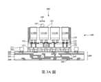
接著,參照第3A圖,將複數個熱介面材料(TIM)薄膜141放置(例如,層壓)在晶粒111的上表面上。熱介面材料薄膜141在放置在晶粒111上之前是預製的。舉例來說,每一個熱介面材料薄膜141在放置在晶粒111上之前被預製成片材(例如,像一張紙一樣的片材格式)。因此,熱介面材料薄膜141也稱為片型(sheet-type)熱介面材料薄膜。Next, referring to FIG. 3A , a plurality of thermal interface material (TIM)
熱介面材料薄膜141由具有高導熱率的合適材料形成。舉例來說,熱介面材料薄膜141可以是石墨烯(graphene)薄膜。熱介面材料薄膜141的厚度可以例如在大約0.1毫米和大約0.2毫米之間的範圍內。在一些實施例中,熱介面材料薄膜141的熱導率介於約10瓦每米.開爾文(watts per meter-kelvin,W/(m.K))和約15W/(m.K)之間。須注意的是,雖然熱介面材料薄膜141在圖式中被示為單層,但是熱介面材料薄膜141可以包括層壓在一起的多個子層。在一些實施例中,複數個熱介面材料薄膜141可以在晶粒111之上堆疊在一起以達到期望的總厚度。The thermal
在一些實施例中,熱介面材料薄膜141由為碳和聚合物的混合物的介電材料形成,其中聚合物可以是例如樹脂基(resin-based)聚合物或丙烯酸基(acrylic-based)聚合物。在一些實施例中,熱介面材料薄膜141的材料中碳的重量百分比介於約40%和約90%之間。在一些實施例中,包含碳和聚合物的熱介面材料薄膜141的熱導率介於約20W/(m.K)和約80W/(m.K)之間,例如23W/(m.K)。可以根據熱介面材料薄膜141的物理性質和性能要求來調整以上揭露的碳的重量百分比的範圍。舉例來說,如果碳百分比低於約40%,則熱介面材料薄膜141的熱導率可能太低。反之,如果碳百分比高於約90%,則熱介面材料薄膜141的彈性及/或粘度可能太低。In some embodiments, the thermal
仍然參照第3A圖,在熱介面材料薄膜141放置在晶粒111上之後,通過在熱介面材料薄膜141上滾動一滾輪147,例如沿著第3A圖中箭頭149的方向,將熱介面材料薄膜141按壓在晶粒111的上表面上。滾輪147的按壓確保熱介面材料薄膜141與晶粒111的上表面緊密接觸,使得熱介面材料薄膜141與晶粒111的上表面之間沒有間隙(例如,氣泡)。這確保了熱介面材料薄膜141與晶粒111之間的接觸面積最大化,從而提高從晶粒111到熱介面材料薄膜141的熱傳遞(例如,散熱)效率。在一些實施例中,省略了用滾輪147按壓熱介面材料薄膜141的步驟。Still referring to Figure 3A, after the thermal
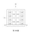
第3B圖示出第3A圖中的半導體裝置200的俯視圖。須注意的是,為簡單起見,未示出半導體裝置200的所有特徵。例如,基板209和被動構件211未被示出。在第3B圖中,晶粒111(例如,晶粒111A和晶粒111B)以虛線顯示,且模製材料135圍繞晶粒111。在第3B圖的範例中,每一個熱介面材料薄膜141完全覆蓋下面的晶粒111(例如,晶粒111A或晶粒111B)的上表面。換句話說,在第3B圖的範例中,熱介面材料薄膜141的數量等於晶粒111的數量,且每一個熱介面材料薄膜141直接在一相應晶粒111之上(例如,直接位於其上並物理接觸)。FIG. 3B shows a top view of the
在第3B圖所示的範例中,每一個熱介面材料薄膜141具有與下面的晶粒111相同的形狀(例如,矩形或方形),且每一個熱介面材料薄膜141的尺寸(例如,寬度和高度)大於下面的晶粒111的尺寸,使得熱介面材料薄膜141延伸超出下面的晶粒111的邊界(例如,側壁)並接觸模製材料135(及/或底部填充材料133)。在其他實施例中,每一個熱介面材料薄膜141的尺寸與下面的晶粒111的尺寸相同,使得在俯視圖中,熱介面材料薄膜141的邊界(例如,側壁)與下面的晶粒111的邊界完全重疊(例如,相同)。因此,在第3B圖的範例中,每一個熱介面材料薄膜141具有與下面的晶粒111相似的幾何形狀。須注意的是,用語”幾何相似”用於包含熱介面材料薄膜141的形狀與下面的晶粒111的形狀相同且具有相同尺寸的實施例,以及熱介面材料薄膜141的形狀是下面的晶粒111的形狀的縮放(例如,放大)版本的實施例。本揭露中的各個實施例的附圖將每一個熱介面材料薄膜141顯示為具有比下面的晶粒111更大的尺寸,然而應理解的是,在一些實施例中熱介面材料薄膜141可以具有與下面的晶粒111相同的尺寸。In the example shown in FIG. 3B , each thermal
仍然參照第3B圖,熱介面材料薄膜141彼此分離(例如,間隔開)。舉例來說,第3B圖示出相鄰的熱介面材料薄膜141之間具有尺寸d2或尺寸d3的間隙,其中d2和d3大於零。第3B圖還示出模製材料135的邊界(例如,側壁)與晶粒111的相應邊界(例如,側壁)之間的距離d1,其中d1大於零。換句話說,在第3B圖的俯視圖中,熱介面材料薄膜141設置在模製材料135的邊界內並與模製材料135的邊界間隔開。在一範例實施例中,所有熱介面材料薄膜141都具有相同的厚度。第3B圖所示的熱介面材料薄膜141的形狀及數量僅為非限制性的範例,其他形狀及/或數量也是可能的且完全有意被包含在本揭露的範圍內。舉例來說,下面討論的第7圖至第10圖示出了其他實施例。Still referring to Figure 3B, the thermal
在晶粒111上使用多個預製的片型熱介面材料薄膜提供優於參考方法(其中,凝膠型(gel-type)熱介面材料沉積在晶粒111上,或單個預形成的(pre-formed)熱介面材料薄膜放置在所有晶粒111上)的優點。細節將在下面討論。The use of multiple preformed sheet-type thermal interface material films on
與凝膠型熱介面材料沉積在晶粒111的上表面上的參考方法相比,本揭露的方法提供多個優點。舉例來說,凝膠型熱介面材料通常具有低熱導率,例如低於3W/(m.K)。相比之下,熱介面材料薄膜141具有高得多的熱導率(例如,大於20W/(m.K))以改善散熱。凝膠型熱介面材料通常需要在較低溫度(例如,-40℃)下儲存,而熱介面材料薄膜141可以在室溫下儲存。為了減少固化的凝膠型熱介面材料與晶粒111之間的空隙(例如,氣泡),凝膠型熱介面材料可能必須以特殊圖案的方式沉積。即使具有特殊圖案,固化的凝膠型熱介面材料中仍可能形成空隙。相比之下,不需要為片型熱介面材料薄膜141設計特殊圖案,且使用本文揭露的實施例不會形成空隙(例如,氣泡)。Compared to the reference method in which a gel-type thermal interface material is deposited on the upper surface of
此外,沉積的凝膠型熱介面材料的形狀和尺寸難以控制,這往往導致晶粒111的低覆蓋率(例如,被熱介面材料覆蓋的晶粒111的上表面面積與未被熱介面材料覆蓋的晶粒111的上表面面積之間的比率),因為晶粒111的上表面的某些區域可能沒有沉積凝膠型熱介面材料。結果,在固化之後,使用凝膠型熱介面材料的覆蓋率較低,例如約83%。相比之下,熱介面材料薄膜141是預先形成的(例如,以片材格式),並可被切割成任何合適的形狀及/或尺寸,從而容易層壓在晶粒111的上表面上。結果,在固化之後,熱介面材料薄膜141對於所有晶粒111實現了大於90%的高覆蓋率,這進而導致晶粒111的散熱改善。由於片型熱介面材料薄膜容易層壓在晶粒111上,故製造過程的產量可遠高於凝膠型沉積在晶粒111上的製程的產量。In addition, the shape and size of the deposited gel-type thermal interface material are difficult to control, which often results in low coverage of the die 111 (e.g., the upper surface area of the die 111 covered by the thermal interface material is less than that of the die 111 that is not covered by the thermal interface material. ratio between the upper surface areas of the die 111), because the upper surface of the die 111Some areas of the surface may not have gel-type thermal interface material deposited. As a result, after curing, the coverage using gel-type thermal interface materials is low, such as about 83%. In contrast, the thermal
與單個片型熱介面材料薄膜層壓在所有晶粒111的頂部上的參考方法相比,本揭露的方法提供額外的優點。半導體裝置100(例如,晶圓上晶片(CoW)結構)在熱循環期間可能發生翹曲,因為晶圓上晶片結構的不同材料具有不同的熱膨脹係數(coefficients of thermal expansion,CTEs)。對於較大尺寸的半導體封裝,翹曲通常較嚴重,且在半導體封裝的周邊附近(例如,靠近側壁)翹曲更嚴重。已經觀察到,當在所有晶粒111上層壓單個大片型熱介面材料薄膜141時,單個熱介面材料薄膜141的周邊部分會承受大應力並可能分層(例如,與位於周邊部分下方的晶粒111的上表面分離),這降低了晶粒111的覆蓋率且導致散熱效率降低。相比之下,本揭露的方法使用多個較小的片型熱介面材料薄膜141來層壓在晶粒111上。由於每一個熱介面材料薄膜141的尺寸較小,在每一個熱介面材料薄膜141上所經歷的翹曲量變化更小,因此,較小的熱介面材料薄膜141較不容易與下面的晶粒111分層,從而提高晶粒111的覆蓋率和散熱效率。測試顯示,通過使用多個較小的熱介面材料薄膜141,在熱介面材料薄膜141固化後可以達到對所有晶粒111的93%或更高的覆蓋率。另外,較小的熱介面材料薄膜141不會增加半導體裝置100中的應力水平,也不會增加半導體裝置100的翹曲。The disclosed method provides additional advantages compared to the reference method in which a single sheet-type thermal interface material film is laminated on top of all dies 111 . Semiconductor devices 100 (eg, wafer-on-wafer (CoW) structures) may warp during thermal cycling because different materials of the wafer-on-wafer structure have different coefficients of thermal expansion (CTEs). Warpage is generally more severe for larger sized semiconductor packages, and is more severe near the perimeter of the semiconductor package (eg, near the sidewalls). It has been observed that when a single large sheet of thermal
接著,在第4圖中,一散熱蓋151(也稱為蓋子)附接到基板209的上表面,以在散熱蓋151與基板209之間形成一封閉空間。蓋子151可以由適合散熱的材料形成,例如銅、鋁、鋼等。在第4圖中,蓋子151具有一頂部151T和數個側壁部分151S。側壁部分151S通過例如膠153附接到基板209的上表面。在一實施例中,蓋子151由金屬材料形成且是電隔離的。在另一實施例中,蓋子151由金屬材料形成且電耦接到導電墊203(例如,通過焊料區域),導電墊203配置為連接到電性接地,在此情況下,蓋子151還用作半導體裝置100的電磁干擾(electro-magnetic interference,EMI)屏蔽。Next, in FIG. 4 , a heat dissipation cover 151 (also called a cover) is attached to the upper surface of the
如第4圖所示,半導體裝置100、熱介面材料薄膜141、以及被動構件211設置在蓋子151與基板209之間的封閉空間中。熱介面材料薄膜141設置在蓋子151的頂部151T與晶粒111的上表面之間。特別地,每一個熱介面材料薄膜141的上表面接觸(例如,物理接觸)頂部151T,且每一個熱介面材料薄膜141的下表面接觸(例如,物理接觸)半導體裝置100的上表面(例如,晶粒111的上表面、模製材料135的上表面及/或底部填充材料133的上表面)。As shown in FIG. 4 , the
接著,在第5圖中,將半導體裝置200夾持在一夾具的頂部治具157和底部治具159之間。可以在頂部治具157與蓋子151之間放置橡膠墊155以防止損壞半導體裝置200。接著,在被夾持在頂部治具157和底部治具159之間的情況下,將半導體裝置200加熱到一預定溫度(例如,介於25℃和150℃之間)並持續一段預定時間(例如,小於1000小時)。加熱製程使熱介面材料薄膜141固化。Next, in FIG. 5 , the
接著,在第6圖中,將半導體裝置200從夾具上取下,並在基板209的下表面的導電墊205上形成導電凸塊207。導電凸塊207可以是焊球、銅柱、其組合等。因此,半導體裝置100、被動構件211、以及導電凸塊207通過基板209的導電特徵(例如,導電線或通孔)電性互連。Next, in FIG. 6 , the
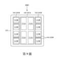
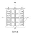
第7圖示出根據一些實施例的半導體裝置200A的俯視圖。半導體裝置200A類似於半導體裝置200,但是熱介面材料薄膜141的數量和形狀不同。舉例來說,與第3B圖的俯視圖相比,第7圖中的半導體裝置200A的晶粒111的一子集(例如,中心區域中的數個晶粒111A)被一較大的熱介面材料薄膜141(標記為141A)覆蓋,而半導體裝置200A的晶粒111的其他多個子集(例如,外圍區域中每兩個相鄰的晶粒111B)被較小的多個熱介面材料薄膜141(標記為141B)覆蓋。Figure 7 illustrates a top view of a
須注意的是,在第7圖中,晶粒111(例如,晶粒111A和晶粒111B)被分組為不同的晶粒子集(subsets),且每一個晶粒111子集被一相應熱介面材料薄膜141(例如,熱介面材料薄膜141A或熱介面材料薄膜141B)覆蓋。每一個熱介面材料薄膜141(例如,熱介面材料薄膜141A或熱介面材料薄膜141B)的形狀依循晶粒111的相應子集的輪廓。在此用語”輪廓(contour)”用於描述由晶粒111的子集的外部邊界定義的形狀。舉例來說,晶粒111A的子集的輪廓是矩形形狀,其中矩形形狀的四個邊由晶粒111A的遠離晶粒111A的子集的中心的外部側壁定義。在第7圖的範例中,每一個熱介面材料薄膜141的尺寸大於下面的晶粒111子集的輪廓,因此,每一個熱介面材料薄膜141的形狀是下面的晶粒111子集的輪廓的縮放(例如,放大)版本。在其他實施例中,每一個熱介面材料薄膜141的尺寸與下面的晶粒111子集的輪廓相同,使得在俯視圖中,熱介面材料薄膜141與下面的晶粒111子集的輪廓完全重疊。因此,每一個熱介面材料薄膜141的形狀是下面的晶粒111子集的輪廓的幾何相似形狀。It should be noted that in FIG. 7 , the die 111 (for example, the
第7圖中的熱介面材料薄膜141A及熱介面材料薄膜141B是片型熱介面材料薄膜,且由與半導體裝置200的熱介面材料薄膜141相同的材料形成。第7圖中的熱介面材料薄膜141A及熱介面材料薄膜141B的尺寸大於第3B圖中的熱介面材料薄膜141的尺寸,但仍小於覆蓋所有晶粒111的單個大熱介面材料薄膜的尺寸。因此,仍可維持上述較小的應力、較少的分層以及提高晶粒111的覆蓋率等優點。另外,由於第7圖中使用的熱介面材料薄膜141的數量減少,用於將熱介面材料薄膜141層壓在晶粒111上的製造時間可以減少。The thermal
在第7圖中,熱介面材料薄膜141A和熱介面材料薄膜141B具有不同的形狀,但由相同的材料形成。在一些實施例中,熱介面材料薄膜141A和熱介面材料薄膜141B具有相同的厚度,例如,因為熱介面材料薄膜141A和熱介面材料薄膜141B是通過將一相同的大片型熱介面材料薄膜切割成具有熱介面材料薄膜141A和熱介面材料薄膜141B的形狀/尺寸的片而形成的。在其他實施例中,熱介面材料薄膜141A和熱介面材料薄膜141B具有不同的厚度。特別地,沿著半導體裝置200A的外圍區域定位的熱介面材料薄膜141B的厚度大於位於半導體裝置200A的中心區域中的熱介面材料薄膜141A的厚度。舉例來說,熱介面材料薄膜141B可以比熱介面材料薄膜141A厚10%到20%。由於半導體裝置200A的外圍區域的翹曲量通常較大,且由於熱介面材料薄膜141B位於外圍區域,因此與熱介面材料薄膜141A相比,熱介面材料薄膜141B的厚度增加,以補償裝置外圍區域增加的翹曲量。較厚的熱介面材料薄膜141B可以有利地減少外圍區域處的熱介面材料薄膜的分層並降低封裝的應力,從而提高散熱效率和形成的裝置的結構完整性。In FIG. 7 , the thermal
第8圖示出根據一些實施例的半導體裝置200B的俯視圖。半導體裝置200B類似於半導體裝置200A,但是晶粒111B的每一個子集包括四個晶粒而不是如第7圖中的兩個晶粒。須注意的是,類似於第7圖,在半導體裝置200B的中心區域之上的熱介面材料薄膜141A可以比在半導體裝置200B的外圍區域之上的熱介面材料薄膜141B更薄。在一些實施例中,熱介面材料薄膜141A和熱介面材料薄膜141B具有相同的厚度。Figure 8 illustrates a top view of a
第9圖示出根據一些實施例的半導體裝置200C的俯視圖。半導體裝置200C類似於半導體裝置200A,但是晶粒111B的一些子集包括兩個晶粒,而晶粒111B的其他子集可以僅包括一個晶粒。須注意的是,類似於第7圖,在半導體裝置200C的中心區域之上的熱介面材料薄膜141A可以比在半導體裝置200C的外圍區域之上的熱介面材料薄膜141B更薄。在一些實施例中,熱介面材料薄膜141A和熱介面材料薄膜141B具有相同的厚度。Figure 9 illustrates a top view of a
第10圖示出根據一些實施例的半導體裝置200D的俯視圖。半導體裝置200D類似於半導體裝置200,但是可僅具有兩個晶粒子集,其中每一個晶粒子集包括位於半導體裝置200D的上表面面積的一半的晶粒111(例如,晶粒111A及晶粒111B)。在一些實施例中,第10圖的熱介面材料薄膜141具有相同的厚度。Figure 10 illustrates a top view of a
第11圖示出根據一些實施例的半導體裝置200E的俯視圖。半導體裝置200E類似於半導體裝置200(參見第3B圖),但是每一個晶粒111B被一熱介面材料薄膜143覆蓋,其中熱介面材料薄膜143由與設置在晶粒111A之上的熱介面材料薄膜141不同的材料形成。換句話說,位於半導體裝置200E的中心區域中的晶粒111A被熱介面材料薄膜141覆蓋,而位於半導體裝置200E的外圍區域中的晶粒111B被熱介面材料薄膜143覆蓋。Figure 11 illustrates a top view of a
在一些實施例中,熱介面材料薄膜141與第3B圖中的熱介面材料薄膜141相同,例如為預形成的片型熱介面材料薄膜,然後被層壓在晶粒111A上。然而,熱介面材料薄膜143則是通過在晶粒111B上施加凝膠型熱介面材料然後固化凝膠型熱介面材料而形成的。凝膠型熱介面材料可以是例如具有金屬填料的黏著劑,例如具有鋁或鋅作為填料的矽凝膠。在一些實施例中,熱介面材料薄膜143比熱介面材料薄膜141厚,以補償半導體封裝的外圍區域增加的翹曲量。半導體裝置200E可以被稱為具有混合式(hybrid)熱介面材料薄膜的半導體封裝。在半導體封裝的外圍區域使用凝膠型熱介面材料可能適用於翹曲較大而無法通過使用厚片型熱介面材料薄膜得到良好補償的封裝。In some embodiments, the thermal
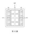
第12圖示出根據一些實施例的半導體裝置200F的俯視圖。半導體裝置200F類似於第11圖的半導體裝置200E,但是具有不同的晶粒111子集。特別地,在半導體裝置200F的中心區域中的四個晶粒111A被一片型熱介面材料薄膜141覆蓋。每一個晶粒111B的子集包括在外圍區域中的兩個晶粒111B,且每一個子集中的晶粒111B被一相應熱介面材料薄膜143覆蓋。Figure 12 illustrates a top view of a
第13圖示出根據一些實施例的半導體裝置200G的俯視圖。半導體裝置200G類似於第12圖的半導體裝置200F,但是具有不同數量的晶粒111子集。特別地,在半導體裝置200G的中心區域中的四個晶粒111A被一片型熱介面材料薄膜141覆蓋。每一個晶粒111B的子集包括在外圍區域中的四個晶粒111B,且每一個子集中的晶粒111B被一相應熱介面材料薄膜143覆蓋。Figure 13 illustrates a top view of a
第14圖示出根據一些實施例的半導體裝置200H的俯視圖。半導體裝置200H類似於第12圖的半導體裝置200F,但是具有不同數量的晶粒111子集。特別地,在半導體裝置200H的中心區域中的四個晶粒111A被一片型熱介面材料薄膜141覆蓋。在外圍區域中的晶粒111B被分組為不同的子集,其中一些子集包括兩個晶粒111B,而其他子集可能僅包括一個晶粒111B。每一個子集中的晶粒111B被一相應熱介面材料薄膜143覆蓋。Figure 14 illustrates a top view of a
本揭露實施例可以實現許多優點。與凝膠型熱介面材料相比,使用片型熱介面材料薄膜141可以實現更高的導熱性以更有效的散熱。熱介面材料薄膜141的形狀和厚度可以容易地控制,以在熱介面材料薄膜141固化後實現對晶粒111的超過93%的優異覆蓋率。由於熱介面材料薄膜141是預製的,因此它很容易在製造過程中使用,以實現比凝膠型熱介面材料更高的產量。與覆蓋所有晶粒111的單個熱介面材料薄膜相比,本揭露的方法使用多個熱介面材料薄膜,每個熱介面材料薄膜覆蓋一個晶粒子集,這允許減小封裝中的應力。觀察到很少或沒有發生熱介面材料薄膜分層,從而增加了晶粒的覆蓋率並提高散熱效率。另外,通過在位於半導體封裝的外圍區域中的晶粒之上使用更厚的熱介面材料薄膜及/或不同材料的熱介面材料薄膜,進一步減少了熱介面材料薄膜的分層並提高裝置完整性。Embodiments of the present disclosure may achieve many advantages. Compared with the gel-type thermal interface material, the use of the sheet-type thermal
第15圖示出根據一些實施例的形成一半導體結構的方法1000的流程圖。應當理解的是,第15圖所示的實施例方法僅是多種可能的實施例方法中的一個範例。本領域中普通技術者可以意識到許多變化、替代和修改。舉例來說,可以添加、去除、取代、重新排序和重複第15圖中所示的各個步驟。Figure 15 illustrates a flowchart of a
參照第15圖,在方塊1010,附接一第一晶粒、一第二晶粒和一第三晶粒到一基板的一第一表面,其中第二晶粒和第三晶粒在第一晶粒的兩相對側。在方塊1020,在第一晶粒、第二晶粒和第三晶粒的周圍形成一模製材料。在方塊1030,在第一晶粒、第二晶粒和第三晶粒上分別形成一第一熱介面材料薄膜、一第二熱介面材料薄膜和一第三熱介面材料薄膜,其中第一熱介面材料薄膜、第二熱介面材料薄膜和第三熱介面材料薄膜彼此間隔開。在方塊1040,附接一散熱蓋到基板的第一表面,以在散熱蓋與基板之間形成一封閉空間,其中第一晶粒、第二晶粒、第三晶粒、第一熱介面材料薄膜、第二熱介面材料薄膜和第三熱介面材料薄膜設置在封閉空間中,其中第一熱介面材料薄膜、第二熱介面材料薄膜和第三熱介面材料薄膜接觸散熱蓋。Referring to Figure 15, at
根據本揭露一些實施例,提供一種半導體結構。所述半導體結構包括一基板、一封裝、複數個熱介面材料薄膜、以及一散熱蓋。封裝附接到基板的一第一表面,其中封裝包括一中介層、複數個晶粒、以及一模製材料,其中中介層的一第一側通過多個第一導電凸塊接合到基板的第一表面,所述晶粒附接到中介層的相對於第一側的一第二側,模製材料在所述晶粒的周圍的中介層的第二側上。所述熱介面材料薄膜在遠離基板的封裝的一第一表面上,其中所述熱介面材料薄膜中的每一者直接設置在所述晶粒中的至少一相應晶粒之上。散熱蓋附接到基板的第一表面,其中封裝和所述熱介面材料薄膜設置在散熱蓋與基板之間的一封閉空間中,其中散熱蓋接觸所述熱介面材料薄膜。在一些實施例中,所述熱介面材料薄膜彼此橫向間隔開。在一些實施例中,在平面圖中,模製材料圍繞所述晶粒,且所述熱介面材料薄膜設置在模製材料的複數個邊界內並與模製材料的所述邊界間隔開。在一些實施例中,所述熱介面材料薄膜係石墨烯薄膜。在一些實施例中,所述熱介面材料薄膜中的每一者設置在所述晶粒中的一相應晶粒之上,並具有與該相應晶粒相似的幾何形狀。在一些實施例中,所述晶粒包括一第一晶粒子集和一第二晶粒子集,其中所述熱介面材料薄膜包括:一第一熱介面材料薄膜,直接設置在第一晶粒子集之上,其中第一熱介面材料薄膜具有與第一晶粒子集的輪廓相似的幾何形狀;以及一第二熱介面材料薄膜,直接設置在第二晶粒子集之上,其中第二熱介面材料薄膜具有與第二晶粒子集的輪廓相似的幾何形狀。在一些實施例中,在俯視圖中,所述晶粒包括:一第一晶粒,在封裝的第一表面的一中心區域中;以及一第二晶粒,在封裝的第一表面的一第一外圍區域中,其中所述熱介面材料薄膜包括直接位於第一晶粒之上的一第一熱介面材料薄膜且包括直接位於第二晶粒之上的一第二熱介面材料薄膜,其中第一熱介面材料薄膜的一第一厚度小於第二熱介面材料薄膜的一第二厚度。在一些實施例中,第一熱介面材料薄膜和第二熱介面材料薄膜包含不同的材料。在一些實施例中,第一熱介面材料薄膜係石墨烯薄膜,第二熱介面材料薄膜係具有金屬填料的黏著劑。在一些實施例中,所述晶粒更包括一第三晶粒,在封裝的第一表面的一第二外圍區域中,第二晶粒和第三晶粒橫向設置在第一晶粒的兩側,其中所述熱介面材料薄膜更包括一第三熱介面材料薄膜,直接位於第三晶粒之上,其中第三熱介面材料薄膜的一第三厚度大於第一熱介面材料薄膜的第一厚度。在一些實施例中,第一熱介面材料薄膜和第二熱介面材料薄膜係不同的材料,其中第二熱介面材料薄膜和第三熱介面材料薄膜係相同的材料。According to some embodiments of the present disclosure, a semiconductor structure is provided. The semiconductor structure includes a substrate, a package, a plurality of thermal interface material films, and a heat dissipation cover. The package is attached to a first surface of the substrate, wherein the package includes an interposer, a plurality of dies, and a molding material, wherein a first side of the interposer is bonded to a first side of the substrate through a plurality of first conductive bumps. A surface with the die attached to a second side of the interposer opposite the first side and molding material on the second side of the interposer around the die. The thermal interface material film is on a first surface of the package remote from the substrate, wherein each of the thermal interface material films is disposed directly on at least a corresponding one of the dies. The heat dissipation cover is attached to the first surface of the substrate, wherein the package and the thermal interface material film are disposed in an enclosed space between the heat dissipation cover and the substrate, and wherein the heat dissipation cover contacts the thermal interface material film. In some embodiments, the thermal interface material films are laterally spaced apart from each other. In some embodiments, mold material surrounds the die in plan view, and the film of thermal interface material is disposed within and spaced from boundaries of the mold material. In some embodiments, the thermal interface material film is a graphene film. In some embodiments, each of the thermal interface material films is disposed over a corresponding one of the dies and has a similar geometry to the corresponding die. In some embodiments, the die includes a first set of die and a second set of die, wherein the thermal interfaceThe material film includes: a first thermal interface material film directly disposed on the first crystal particle set, wherein the first thermal interface material film has a geometric shape similar to the outline of the first crystal particle set; and a second thermal interface material film. The thermal interface material film is directly disposed on the second set of crystal particles, wherein the second thermal interface material film has a geometric shape similar to the outline of the second set of crystal particles. In some embodiments, in a top view, the die includes: a first die in a central region of the first surface of the package; and a second die in a first surface of the package. In a peripheral region, wherein the thermal interface material film includes a first thermal interface material film directly on the first die and includes a second thermal interface material film directly on the second die, wherein the A first thickness of a thermal interface material film is smaller than a second thickness of a second thermal interface material film. In some embodiments, the first thermal interface material film and the second thermal interface material film include different materials. In some embodiments, the first thermal interface material film is a graphene film, and the second thermal interface material film is an adhesive with metal fillers. In some embodiments, the die further includes a third die, and in a second peripheral area of the first surface of the package, the second die and the third die are laterally disposed on both sides of the first die. side, wherein the thermal interface material film further includes a third thermal interface material film directly located on the third die, wherein a third thickness of the third thermal interface material film is greater than the first thickness of the first thermal interface material film. thickness. In some embodiments, the first thermal interface material film and the second thermal interface material film are different materials, wherein the second thermal interface material film and the third thermal interface material film are the same material.
根據本揭露一些實施例,提供一種半導體結構。所述半導體結構包括一基板、一第一晶粒、一第二晶粒、一第三晶粒、一模製材料、一散熱蓋、以及複數個熱介面材料薄膜。第一晶粒、第二晶粒和第三晶粒附接到基板的一第一側,其中第二晶粒和第三晶粒橫向設置在第一晶粒的兩側。模製材料在基板的第一側之上,其中第一晶粒、第二晶粒和第三晶粒內埋在模製材料中。散熱蓋附接到基板的第一側,其中第一晶粒、第二晶粒和第三晶粒在散熱蓋與基板之間的一封閉空間中。所述熱介面材料薄膜在散熱蓋與第一晶粒、第二晶粒和第三晶粒之間,其中所述熱介面材料薄膜包括分別設置在第一晶粒、第二晶粒和第三晶粒之上的一第一熱介面材料薄膜、一第二熱介面材料薄膜和一第三熱介面材料薄膜,其中所述熱介面材料薄膜彼此橫向間隔開。在一些實施例中,所述熱介面材料薄膜中的每一者具有與下面的晶粒相似的幾何形狀。在一些實施例中,所述半導體結構更包括一第四晶粒,附接到基板的第一側,其中第二晶粒和第四晶粒在第一晶粒的同一側,其中第一熱介面材料薄膜覆蓋第一晶粒並具有與第一晶粒相似的一第一幾何形狀,其中第二熱介面材料薄膜覆蓋第二晶粒和第四晶粒並具有與第二晶粒和第四晶粒的輪廓相似的一第二幾何形狀。在一些實施例中,第一熱介面材料薄膜的一第一厚度小於第二熱介面材料薄膜的一第二厚度且小於第三熱介面材料薄膜的一第三厚度。在一些實施例中,第二厚度與第三厚度相同。在一些實施例中,第一熱介面材料薄膜由一第一材料形成,其中第二熱介面材料薄膜和第三熱介面材料薄膜由不同於第一材料的一第二材料形成。According to some embodiments of the present disclosure, a semiconductor structure is provided. The semiconductor structure includes a substrate, a first die, a second die, a third die, a molding material, a heat dissipation cover, and a plurality of thermal interface material films. The first die, the second die and the third die are attached to a first side of the substrate, wherein the second die and the third die are laterally disposed on both sides of the first die. A molding material is over the first side of the substrate, wherein the first die, the second die and the third die are embedded in the molding materialmiddle. The heat dissipation cover is attached to the first side of the substrate, with the first die, the second die and the third die in an enclosed space between the heat dissipation cover and the substrate. The thermal interface material film is between the heat dissipation cover and the first die, the second die and the third die, wherein the thermal interface material film includes components respectively provided on the first die, the second die and the third die. A first thermal interface material film, a second thermal interface material film and a third thermal interface material film on the die, wherein the thermal interface material films are laterally spaced apart from each other. In some embodiments, each of the thermal interface material films has a similar geometry to the underlying die. In some embodiments, the semiconductor structure further includes a fourth die attached to the first side of the substrate, wherein the second die and the fourth die are on the same side of the first die, wherein the first thermal die The interface material film covers the first die and has a first geometric shape similar to the first die, wherein the second thermal interface material film covers the second die and the fourth die and has a similar shape to the second die and the fourth die. The grain profile is similar to a second geometric shape. In some embodiments, a first thickness of the first thermal interface material film is less than a second thickness of the second thermal interface material film and less than a third thickness of the third thermal interface material film. In some embodiments, the second thickness and the third thickness are the same. In some embodiments, the first thermal interface material film is formed of a first material, and the second thermal interface material film and the third thermal interface material film are formed of a second material different from the first material.
根據本揭露一些實施例,提供一種形成半導體結構的方法。所述方法包括附接一第一晶粒、一第二晶粒和一第三晶粒到一基板的一第一表面,其中第二晶粒和第三晶粒在第一晶粒的兩側。所述方法還包括形成圍繞第一晶粒、第二晶粒和第三晶粒的一模製材料。所述方法還包括在第一晶粒、第二晶粒和第三晶粒上分別形成一第一熱介面材料薄膜、一第二熱介面材料薄膜和一第三熱介面材料薄膜,其中第一熱介面材料薄膜、第二熱介面材料薄膜和第三熱介面材料薄膜彼此間隔開。此外,所述方法包括附接一散熱蓋到基板的第一表面,以在散熱蓋與基板之間形成一封閉空間,其中第一晶粒、第二晶粒、第三晶粒、第一熱介面材料薄膜、第二熱介面材料薄膜和第三熱介面材料薄膜設置在封閉空間中,其中第一熱介面材料薄膜、第二熱介面材料薄膜和第三熱介面材料薄膜接觸散熱蓋。在一些實施例中,形成第一熱介面材料薄膜、第二熱介面材料薄膜和第三熱介面材料薄膜包括將一第一預形成熱介面材料片(pre-formed TIM sheet)、一第二預形成熱介面材料片和一第三預形成熱介面材料片分別放置在第一晶粒、第二晶粒和第三晶粒上,其中第二預形成熱介面材料片和第三預形成熱介面材料片比第一預形成熱介面材料片厚。在一些實施例中,形成第一熱介面材料薄膜、第二熱介面材料薄膜和第三熱介面材料薄膜包括:將一預形成片型熱介面材料放置在第一晶粒上;以及將一凝膠型熱介面材料分配在第二晶粒和第三晶粒上,其中預形成片型熱介面材料和凝膠型熱介面材料包含不同的材料。According to some embodiments of the present disclosure, a method of forming a semiconductor structure is provided. The method includes attaching a first die, a second die and a third die to a first surface of a substrate, wherein the second die and the third die are on both sides of the first die . The method also includes forming a molding material surrounding the first die, the second die, and the third die. The method further includes forming a first thermal interface material film, a second thermal interface material film and a third thermal interface material film on the first die, the second die and the third die respectively, wherein the first The thermal interface material film, the second thermal interface material film and the third thermal interface material film are spaced apart from each other. Additionally, the method includes attaching a thermal cover to the substrateThe first surface is to form a closed space between the heat dissipation cover and the substrate, wherein the first die, the second die, the third die, the first thermal interface material film, the second thermal interface material film and the third thermal interface material are The interface material film is disposed in a closed space, wherein the first thermal interface material film, the second thermal interface material film and the third thermal interface material film contact the heat dissipation cover. In some embodiments, forming the first thermal interface material film, the second thermal interface material film and the third thermal interface material film includes combining a first pre-formed thermal interface material sheet (pre-formed TIM sheet), a second pre-formed TIM sheet Forming a thermal interface material sheet and a third pre-formed thermal interface material sheet are respectively placed on the first die, the second die and the third die, wherein the second pre-formed thermal interface material sheet and the third pre-formed thermal interface material sheet are placed on the first die, the second die and the third die respectively. The sheet of material is thicker than the first preformed thermal interface material sheet. In some embodiments, forming the first thermal interface material film, the second thermal interface material film and the third thermal interface material film includes: placing a preformed sheet thermal interface material on the first die; and placing a solid The gel-type thermal interface material is distributed on the second die and the third die, wherein the preformed sheet-type thermal interface material and the gel-type thermal interface material include different materials.
前述內文概述了許多實施例的特徵,使本技術領域中具有通常知識者可以從各個方面更佳地了解本揭露。本技術領域中具有通常知識者應可理解,且可輕易地以本揭露為基礎來設計或修飾其他製程及結構,並以此達到相同的目的及/或達到與在此介紹的實施例等相同之優點。本技術領域中具有通常知識者也應了解這些相等的結構並未背離本揭露的發明精神與範圍。在不背離本揭露的發明精神與範圍之前提下,可對本揭露進行各種改變、置換或修改。The foregoing text summarizes the features of many embodiments so that those skilled in the art can better understand the present disclosure from various aspects. It should be understood by those with ordinary skill in the art that other processes and structures can be easily designed or modified based on this disclosure to achieve the same purpose and/or achieve the same results as the embodiments introduced here. The advantages. Those of ordinary skill in the art should also understand that these equivalent structures do not depart from the spirit and scope of the present disclosure. Various changes, substitutions, or modifications may be made to the disclosure without departing from the spirit and scope of the disclosure.
111A,111B:晶粒111A, 111B: grain
135:模製材料135: Molding materials
141:(片型)熱介面材料薄膜141: (sheet type) thermal interface material film
200:半導體裝置200:Semiconductor devices
d1:距離d1: distance
d2,d3:尺寸d2,d3: size
Claims (9)
Translated fromChineseApplications Claiming Priority (4)
| Application Number | Priority Date | Filing Date | Title |
|---|---|---|---|
| US202163193855P | 2021-05-27 | 2021-05-27 | |
| US63/193,855 | 2021-05-27 | ||
| US17/370,591US12300568B2 (en) | 2021-05-27 | 2021-07-08 | High efficiency heat dissipation using discrete thermal interface material films |
| US17/370,591 | 2021-07-08 |
Publications (2)
| Publication Number | Publication Date |
|---|---|
| TW202247366A TW202247366A (en) | 2022-12-01 |
| TWI811990Btrue TWI811990B (en) | 2023-08-11 |
Family
ID=83325035
Family Applications (1)
| Application Number | Title | Priority Date | Filing Date |
|---|---|---|---|
| TW111104263ATWI811990B (en) | 2021-05-27 | 2022-02-07 | Semiconductor structure and method for forming the same |
Country Status (5)
| Country | Link |
|---|---|
| US (3) | US12300568B2 (en) |
| KR (1) | KR102734792B1 (en) |
| CN (1) | CN115116987A (en) |
| DE (1) | DE102021117989A1 (en) |
| TW (1) | TWI811990B (en) |
Families Citing this family (5)
| Publication number | Priority date | Publication date | Assignee | Title |
|---|---|---|---|---|
| US11784061B2 (en)* | 2021-02-25 | 2023-10-10 | Taiwan Semiconductor Manufacturing Company, Ltd. | Chip package structure and method for forming the same |
| US20240347413A1 (en)* | 2023-04-11 | 2024-10-17 | Micron Technology, Inc. | Thermally regulated semiconductor device |
| TWI845267B (en)* | 2023-04-20 | 2024-06-11 | 宜鼎國際股份有限公司 | High capacitance module |
| US20240371774A1 (en)* | 2023-05-01 | 2024-11-07 | Taiwan Semiconductor Manufacturing Company Limited | Package module including a recessed upper surface and methods of forming the package module |
| US12332001B1 (en) | 2024-05-08 | 2025-06-17 | Jentech Precision Industrial Co., Ltd. | Method of manufacturing heat dissipation module |
Citations (3)
| Publication number | Priority date | Publication date | Assignee | Title |
|---|---|---|---|---|
| US20140264820A1 (en)* | 2013-03-13 | 2014-09-18 | Wei Hu | Paste thermal interface materials |
| US20200219786A1 (en)* | 2019-01-08 | 2020-07-09 | Taiwan Semiconductor Manufacturing Company, Ltd. | Package Structure and Method and Equipment for Forming the Same |
| US20200286809A1 (en)* | 2019-03-05 | 2020-09-10 | Intel Corporation | Carbon-pad thermal-interface materials in multi-die packages |
Family Cites Families (22)
| Publication number | Priority date | Publication date | Assignee | Title |
|---|---|---|---|---|
| US7312261B2 (en)* | 2004-05-11 | 2007-12-25 | International Business Machines Corporation | Thermal interface adhesive and rework |
| US7939368B2 (en) | 2006-03-07 | 2011-05-10 | Stats Chippac Ltd. | Wafer level chip scale package system with a thermal dissipation structure |
| US20070219312A1 (en) | 2006-03-17 | 2007-09-20 | Jennifer Lynn David | Silicone adhesive composition and method for preparing the same |
| US20090068441A1 (en) | 2007-08-31 | 2009-03-12 | Swaroop Srinivas H | Thermal interface materials |
| US8202765B2 (en)* | 2009-01-22 | 2012-06-19 | International Business Machines Corporation | Achieving mechanical and thermal stability in a multi-chip package |
| US8797057B2 (en) | 2011-02-11 | 2014-08-05 | Taiwan Semiconductor Manufacturing Company, Ltd. | Testing of semiconductor chips with microbumps |
| US9443783B2 (en) | 2012-06-27 | 2016-09-13 | Taiwan Semiconductor Manufacturing Company, Ltd. | 3DIC stacking device and method of manufacture |
| US20140138854A1 (en)* | 2012-11-21 | 2014-05-22 | Hitesh Arora | Thermal interface material for integrated circuit package assembly and associated techniques and configurations |
| US9299649B2 (en) | 2013-02-08 | 2016-03-29 | Taiwan Semiconductor Manufacturing Company, Ltd. | 3D packages and methods for forming the same |
| US8993380B2 (en) | 2013-03-08 | 2015-03-31 | Taiwan Semiconductor Manufacturing Company, Ltd. | Structure and method for 3D IC package |
| JP2015088683A (en) | 2013-11-01 | 2015-05-07 | 富士通株式会社 | Thermal bonding sheet and processor |
| US9281254B2 (en) | 2014-02-13 | 2016-03-08 | Taiwan Semiconductor Manufacturing Company, Ltd. | Methods of forming integrated circuit package |
| US9425126B2 (en) | 2014-05-29 | 2016-08-23 | Taiwan Semiconductor Manufacturing Company, Ltd. | Dummy structure for chip-on-wafer-on-substrate |
| US9496189B2 (en) | 2014-06-13 | 2016-11-15 | Taiwan Semiconductor Manufacturing Company, Ltd. | Stacked semiconductor devices and methods of forming same |
| US9666502B2 (en) | 2015-04-17 | 2017-05-30 | Taiwan Semiconductor Manufacturing Company, Ltd. | Discrete polymer in fan-out packages |
| US9461018B1 (en) | 2015-04-17 | 2016-10-04 | Taiwan Semiconductor Manufacturing Company, Ltd. | Fan-out PoP structure with inconsecutive polymer layer |
| US9735131B2 (en) | 2015-11-10 | 2017-08-15 | Taiwan Semiconductor Manufacturing Company, Ltd. | Multi-stack package-on-package structures |
| WO2017123188A1 (en)* | 2016-01-11 | 2017-07-20 | Intel Corporation | Multiple-chip package with multiple thermal interface materials |
| WO2019161282A1 (en)* | 2018-02-17 | 2019-08-22 | Laird Technologies, Inc. | Thermal interface materials having high dielectric losses and low dielectric constants |
| US10978373B2 (en) | 2018-06-19 | 2021-04-13 | Taiwan Semiconductor Manufacturing Company, Ltd. | Semiconductor device methods of manufacture |
| US10971461B2 (en) | 2018-08-16 | 2021-04-06 | Taiwan Semiconductor Manufacturing Company, Ltd. | Semiconductor device and method of manufacture |
| US11728238B2 (en) | 2019-07-29 | 2023-08-15 | Taiwan Semiconductor Manufacturing Company, Ltd. | Semiconductor package with heat dissipation films and manufacturing method thereof |
- 2021
- 2021-07-08USUS17/370,591patent/US12300568B2/enactiveActive
- 2021-07-13DEDE102021117989.0Apatent/DE102021117989A1/enactivePending
- 2022
- 2022-01-29CNCN202210110675.6Apatent/CN115116987A/enactivePending
- 2022-02-07TWTW111104263Apatent/TWI811990B/enactive
- 2022-02-22KRKR1020220023043Apatent/KR102734792B1/enactiveActive
- 2023
- 2023-07-27USUS18/360,484patent/US12424511B2/enactiveActive
- 2024
- 2024-07-25USUS18/784,233patent/US20240379494A1/enactivePending
Patent Citations (3)
| Publication number | Priority date | Publication date | Assignee | Title |
|---|---|---|---|---|
| US20140264820A1 (en)* | 2013-03-13 | 2014-09-18 | Wei Hu | Paste thermal interface materials |
| US20200219786A1 (en)* | 2019-01-08 | 2020-07-09 | Taiwan Semiconductor Manufacturing Company, Ltd. | Package Structure and Method and Equipment for Forming the Same |
| US20200286809A1 (en)* | 2019-03-05 | 2020-09-10 | Intel Corporation | Carbon-pad thermal-interface materials in multi-die packages |
Also Published As
| Publication number | Publication date |
|---|---|
| DE102021117989A1 (en) | 2022-12-01 |
| US20220384304A1 (en) | 2022-12-01 |
| US12300568B2 (en) | 2025-05-13 |
| KR20220160466A (en) | 2022-12-06 |
| KR102734792B1 (en) | 2024-11-26 |
| US12424511B2 (en) | 2025-09-23 |
| TW202247366A (en) | 2022-12-01 |
| CN115116987A (en) | 2022-09-27 |
| US20230369164A1 (en) | 2023-11-16 |
| US20240379494A1 (en) | 2024-11-14 |
Similar Documents
| Publication | Publication Date | Title |
|---|---|---|
| TWI811990B (en) | Semiconductor structure and method for forming the same | |
| US20240153842A1 (en) | Integrated Fan-Out Packages with Embedded Heat Dissipation Structure | |
| TWI710072B (en) | Semiconductor device package and method of forming the same | |
| KR20250057757A (en) | Integrated circuit package and method | |
| CN113363244B (en) | Semiconductor structure and method for forming the same | |
| CN108695175B (en) | Manufacturing method of semiconductor structure | |
| CN112687665B (en) | Semiconductor device and method for forming the same | |
| TWI732278B (en) | Semiconductor device and method of forming the same | |
| TW202117869A (en) | Package structure and method for forming the same | |
| US20240371725A1 (en) | High efficiency heat dissipation using thermal interface material film | |
| CN110660752A (en) | Semiconductor device package and method of manufacturing the same | |
| TW202234608A (en) | Package structure | |
| TWI886497B (en) | Semiconductor device and method for manufacturing the same | |
| TW202401712A (en) | Semiconductor package |