TWI811151B - Method for managing memory write request in cache device - Google Patents
Method for managing memory write request in cache deviceDownload PDFInfo
- Publication number
- TWI811151B TWI811151BTW111142793ATW111142793ATWI811151BTW I811151 BTWI811151 BTW I811151BTW 111142793 ATW111142793 ATW 111142793ATW 111142793 ATW111142793 ATW 111142793ATW I811151 BTWI811151 BTW I811151B
- Authority
- TW
- Taiwan
- Prior art keywords
- memory
- request
- write
- data
- write request
- Prior art date
Links
Images


Classifications
- G—PHYSICS
- G06—COMPUTING OR CALCULATING; COUNTING
- G06F—ELECTRIC DIGITAL DATA PROCESSING
- G06F12/00—Accessing, addressing or allocating within memory systems or architectures
- G06F12/02—Addressing or allocation; Relocation
- G06F12/08—Addressing or allocation; Relocation in hierarchically structured memory systems, e.g. virtual memory systems
- G06F12/0802—Addressing of a memory level in which the access to the desired data or data block requires associative addressing means, e.g. caches
- G06F12/0806—Multiuser, multiprocessor or multiprocessing cache systems
- G06F12/0815—Cache consistency protocols
- G06F12/0831—Cache consistency protocols using a bus scheme, e.g. with bus monitoring or watching means
- G06F12/0833—Cache consistency protocols using a bus scheme, e.g. with bus monitoring or watching means in combination with broadcast means (e.g. for invalidation or updating)
- G—PHYSICS
- G06—COMPUTING OR CALCULATING; COUNTING
- G06F—ELECTRIC DIGITAL DATA PROCESSING
- G06F12/00—Accessing, addressing or allocating within memory systems or architectures
- G06F12/02—Addressing or allocation; Relocation
- G06F12/08—Addressing or allocation; Relocation in hierarchically structured memory systems, e.g. virtual memory systems
- G06F12/0802—Addressing of a memory level in which the access to the desired data or data block requires associative addressing means, e.g. caches
- G06F12/0893—Caches characterised by their organisation or structure
- G06F12/0897—Caches characterised by their organisation or structure with two or more cache hierarchy levels
- G—PHYSICS
- G06—COMPUTING OR CALCULATING; COUNTING
- G06F—ELECTRIC DIGITAL DATA PROCESSING
- G06F13/00—Interconnection of, or transfer of information or other signals between, memories, input/output devices or central processing units
- G06F13/14—Handling requests for interconnection or transfer
- G06F13/16—Handling requests for interconnection or transfer for access to memory bus
- G06F13/1668—Details of memory controller
- G06F13/1673—Details of memory controller using buffers
Landscapes
- Engineering & Computer Science (AREA)
- Theoretical Computer Science (AREA)
- Physics & Mathematics (AREA)
- General Engineering & Computer Science (AREA)
- General Physics & Mathematics (AREA)
- Memory System Of A Hierarchy Structure (AREA)
Abstract
Description
Translated fromChinese本發明是有關於一種電腦系統中快取裝置的管理方法,且特別是有關於一種電腦系統的快取裝置中管理記憶體寫入要求的方法。The present invention relates to a management method of a cache device in a computer system, and in particular to a method for managing memory writing requirements in a cache device of a computer system.
在電腦系統中,中央處理器(CPU)以及系統記憶體(system memory)的運作速度差異很大。中央處理器存取(access)系統記憶體時通常會耗費時間等待系統記憶體進行存取動作。因此,在電腦系統中,中央處理器與系統記憶體之間加入了存取速度快於系統記憶體的快取裝置(cache device)。當然,快取裝置也可以直接設計於中央處理器內部。In a computer system, the operating speeds of the central processing unit (CPU) and system memory (system memory) vary widely. When the CPU accesses the system memory, it usually spends time waiting for the system memory to perform the access action. Therefore, in the computer system, a cache device (cache device) whose access speed is faster than the system memory is added between the central processing unit and the system memory. Of course, the cache device can also be directly designed inside the central processing unit.
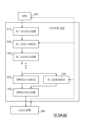
請參照第1圖,其所繪示為習知電腦系統中的快取裝置示意圖。快取裝置170耦接(couple to)至中央處理器150,且快取裝置170經由匯流排(bus) 耦接至系統記憶體160。中央處理器150可連續發出多筆要求(request)來存取(access)系統記憶體160。當該筆要求為記憶體寫入要求(memory write request)時,該筆要求會包括位址資訊(address information)與寫入資料(write data)。當要求為記憶體讀取要求(memory read request)時,該筆要求中會包括位址資訊(address information)。Please refer to FIG. 1, which shows a schematic diagram of a cache device in a conventional computer system. The
在快取裝置中,每一個快取記憶體112、122、132內皆包括多條快取線(cache line)。舉例來說,第二級快取記憶體122中有M條快取線,每一條快取線至少可記錄位址資訊與儲存資料。M為大於1的整數。當然,每一個快取記憶體112、122、132中可以有不同數目的快取線。In the cache device, each
當中央處理器150發出一筆要求至系統記憶體160時,快取裝置170會接收並判斷快取記憶體112、122、132的所有快取線內是否記錄相同的位址資訊。如果快取記憶體112、122、132的其中一條快取線記錄的位址資訊相同於該筆要求中的位址資訊時,則視為命中(hit)。反之,如果快取記憶體112、122、132中所有快取線記錄的位址資訊皆異於該筆要求中的位址資訊時,則為未命中(miss)。以下簡單地區分為各種狀況。When the
於命中(hit)的情況下,如果該筆要求為記憶體讀取要求,快取裝置170將快取記憶體112、122、132中對應快取線的儲存資料作為讀取資料(read data),並回傳至中央處理器150。In the case of a hit (hit), if the request is a memory read request, the
於命中(hit)的情況下,如果該筆要求為記憶體寫入要求,則快取裝置170將寫入資料更新(update)於快取記憶體112、122、132中對應快取線內。亦即,對應快取線中的儲存資料會被更新。In the case of a hit, if the request is a memory write request, the
於未命中(miss)的情況,如果該筆要求為記憶體讀取要求,則快取裝置170會將該筆要求傳遞至系統記憶體160。當系統記憶體160回傳讀取資料時,讀取資料會傳遞至中央處理器150與快取裝置170。而快取裝置170會在快取記憶體112、122、132尋找一條可用快取線(available cache line),例如空白快取線(empty cache line),來儲存位址資訊以及讀取資料。In case of a miss, if the request is a memory read request, the
另外,於未命中(miss)的情況,如果該筆要求為記憶體寫入要求,則快取裝置170會將該筆要求傳遞至系統記憶體160,並將寫入資料更新(update)至系統記憶體160。以下更詳細地說明快取裝置170的運作。In addition, in the case of a miss, if the request is a memory write request, the
如第1圖所示,快取裝置170中區分為很多級(level),例如N級。因此,快取裝置170包括:第一級快取記憶體(L1cache memory)112、第二級指令緩衝器(L2command buffer)120、第二級快取記憶體(L2cache memory)122、第N級指令緩衝器(LNcommand buffer)130以及第N級快取記憶體(LNcache memory)132。其中,N為大於1的整數,第N級指令緩衝器130與第N級快取記憶體132為快取裝置170中最後一級指令緩衝器以及最後一級快取記憶體。As shown in FIG. 1 , the
當中央處理器150發出要求(request)至快取裝置170時,快取裝置170會先判斷是否命中(hit)第一級快取記憶體112。When the
於命中的情況下,如果該筆要求為記憶體讀取要求,則第一級快取記憶體112中對應快取線的儲存資料即為讀取資料,並回傳讀取資料至中央處理器150,且該筆記憶體讀取要求被退休(retired),代表該筆記憶體讀取要求已經完成。In the case of a hit, if the request is a memory read request, then the storage data corresponding to the cache line in the first-
於命中的情況下,如果該筆要求為記憶體寫入要求,則將寫入資料更新(update)於第一級快取記憶體112的對應快取線內,亦即對應快取線中的儲存資料會被更新。接著,該筆記憶體寫入要求被退休(retired),代表該筆記憶體寫入要求已經完成。In the case of a hit, if the request is a memory write request, the write data is updated (update) in the corresponding cache line of the first-
於未命中的情況下,該筆要求會被傳送至第二級指令緩衝器120。第二級指令緩衝器120中包括多個入口(entry),每一個入口可暫存一筆要求。也就是說,當該筆要求會被傳送至第二級指令緩衝器120時,該筆要求會被暫存於第二級指令緩衝器120中的一個自由入口(free entry)。基本上,當一個入口已經暫存一筆要求時,該入口被視為一個使用入口(used entry)。當一個入口尚未儲存要求時,該入口被視為一自由入口(free entry)。再者,第二級指令緩衝器120與第二級快取記憶體122相互搭配。In case of a miss, the request is sent to the second-
快取裝置170可選擇第二級指令緩衝器120中多個使用入口(used entry)的其中一筆要求,並判斷是否命中第二級快取記憶體122。The
舉例來說,快取裝置170選擇第二級指令緩衝器120中的一筆要求並判斷是否命中第二級快取記憶體122。於命中的情況下,如果該筆要求為記憶體讀取要求,則第二級快取記憶體122中對應快取線的儲存資料即為讀取資料,並回傳讀取資料至中央處理器150,且該筆記憶體讀取要求被退休(retired),代表該筆記憶體讀取要求已經完成。For example, the
於命中的情況下,如果該筆要求為記憶體寫入要求,則將寫入資料更新於第二級快取記憶體122的對應快取線內,亦即對應快取線中的儲存資料會被更新。接著,該筆記憶體寫入要求被退休(retired),代表該筆記憶體寫入要求已經完成。基本上,當要求被退休時,對應使用入口(used entry)的內容會被清空(clear)或者被設定為無效(invalid),並成為自由入口(free entry)可在未來暫存新的要求。In the case of a hit, if the request is a memory write request, the write data will be updated in the corresponding cache line of the second-
另外,於未命中的情況下,該筆要求會被傳送至下一級指令緩衝器。類似地,下一級指令緩衝器包括多個入口(entry)可暫存多個要求,每一個入口可暫存一筆要求。也就是說,當該筆要求會被傳送至下一級指令緩衝器時,該筆要求會被暫存於下一級指令緩衝器中的一個自由入口。再者,下一級指令緩衝器與下一級快取記憶體相互搭配。其運作模式類似於第二級指令緩衝器120與第二級快取記憶體122。此處不再贅述。In addition, in case of a miss, the request will be sent to the next level instruction buffer. Similarly, the next-level instruction buffer includes multiple entries to temporarily store multiple requests, and each entry can temporarily store one request. That is to say, when the request is sent to the next-level instruction buffer, the request is temporarily stored in a free entry in the next-level instruction buffer. Furthermore, the next-level instruction buffer and the next-level cache memory are matched with each other. Its operation mode is similar to the second-
在一直未命中的情況下,該筆要求最後會被傳送至第N級指令緩衝器130。第N級指令緩衝器130包括多個入口(entry)可暫存多個要求,每一個入口可暫存一筆要求。也就是說,當該筆要求會被傳送至第N級指令緩衝器130時,該筆要求會被暫存於第N級指令緩衝器130中的一個自由入口(free entry)。再者,第N級指令緩衝器130與第N級快取記憶體132相互搭配。In the case of a miss all the time, the request will be sent to the Nth-
類似地,快取裝置170可選擇第N級指令緩衝器130中多個使用入口(used entry)內的其中一筆要求,並判斷 該筆要求是否命中第N級快取記憶體132。Similarly, the
舉例來說,快取裝置170選擇第N級指令緩衝器130中的一筆要求並判斷命中是否第N級快取記憶體132。於命中的情況下,如果該筆要求為記憶體讀取要求,則第N級快取記憶體132中對應快取線的儲存資料即為讀取資料,並回傳讀取資料至中央處理器150,且該筆記憶體讀取要求被退休(retired),代表該筆記憶體讀取要求已經完成。For example, the
於命中的情況下,如果該筆要求為記憶體寫入要求,則將寫入資料更新於第N級快取記憶體132的對應快取線內,亦即對應快取線中的儲存資料會被更新。接著,該筆記憶體寫入要求被退休(retired),代表該筆記憶體寫入要求已經完成。In the case of a hit, if the request is a memory write request, the written data will be updated in the corresponding cache line of the Nth
另外,於未命中的情況下,該筆要求會被傳送並系統記憶體160。舉例來說,於未命中的情況下,快取裝置170將記憶體讀取要求傳送至統記憶體160後,系統記憶體160根據記憶體讀取要求產生讀取資料並回傳至中央處理器150與快取裝置170。此時,快取裝置170即結合該筆記憶體讀取要求中的位址資訊以及回傳的讀取資料,並選擇快取記憶體112、122、132的至少一條可用快取線(available cacheline)來儲存位址資訊以及讀取資要。之後,該筆記憶體讀取要求被退休(retired),代表該筆記憶體讀取要求已經完成。In addition, in case of a miss, the request will be sent to the
或者,快取裝置170將記憶體寫入要求傳送至統記憶體160後,該筆記憶體寫入要求被退休(retired),代表該筆記憶體寫入要求已經完成。另外,系統記憶體160即根據記憶體寫入要求中的位址資訊,將寫入資料更新於系統記憶體160。Alternatively, after the
眾所周知,電腦系統在運作的過程中,中央處理器150會持續地發出要求。因此,快取裝置170中的所有指令緩衝器120、130會持續地接收並暫存要求、執行要求、退休要求或者將要求傳送至下一級。As we all know, during the operation of the computer system, the
本發明的目的在於修改上述電腦系統的快取裝置及提供管理記憶體寫入要求的方法。The object of the present invention is to modify the cache device of the above computer system and provide a method for managing memory write requests.
本發明係有關於一種運用於快取裝置中管理一記憶體寫入要求的方法,該快取裝置耦接於一中央處理器與一系統記憶體之間,該快取裝置包括複數級,且一第N級包括一第N級指令緩衝器、一第N級快取記憶體與一寫入配置緩衝器,N為大於1的整數,該方法包括下列步驟:接收一前一級傳送的一要求;當該要求為一記憶體寫入要求時,將該記憶體寫入要求暫存至該寫入配置緩衝器中的一自由入口,其中該記憶體寫入要求包括一位址資訊與一寫入資料;以及,當該要求不是該記憶體寫入要求時,將該要求暫存至該第N級指令緩衝器中的一自由入口。The present invention relates to a method for managing a memory write request applied in a cache device coupled between a central processing unit and a system memory, the cache device includes a plurality of stages, and An Nth stage includes an Nth stage instruction buffer, an Nth stage cache memory, and a write configuration buffer, N is an integer greater than 1, and the method includes the following steps: receiving a request from a previous stage ; When the request is a memory write request, temporarily store the memory write request to a free entry in the write configuration buffer, wherein the memory write request includes an address information and a write and, when the request is not the memory write request, temporarily storing the request to a free entry in the Nth-level instruction buffer.
本發明係有關於一種運用於快取裝置中管理一記憶體寫入要求的方法,該快取裝置耦接於一中央處理器與一系統記憶體之間,該快取裝置包括複數級,且一第N級包括一第N級指令緩衝器、一第N級快取記憶體與一寫入配置緩衝器,N為大於1的整數,該方法包括下列步驟:(a)接收一前一級傳送的一要求;(b)當該要求不是一記憶體寫入要求時,將該要求暫存至該第N級指令緩衝器中的一自由入口;(c)當該要求為該記憶體寫入要求時,將該記憶體寫入要求傳送至該寫入配置緩衝器,其中該記憶體寫入要求包括一位址資訊與一寫入資料;(d)當該寫入配置緩衝器中所有使用入口皆未記錄相同的該位址資訊時,將該記憶體寫入要求暫存至該寫入配置緩衝器中的一自由入口;(e)當該寫入配置緩衝器中僅有一特定使用入口記錄相同的該位址資訊,且該寫入資料可以合併時,將該記憶體寫入要求的該寫入資料合併至該特定使用入口的一儲存資料,並退休該記憶體寫入要求;(f)當該寫入配置緩衝器中僅有該特定使用入口記錄相同的該位址資訊,且該寫入資料不可以合併時,將該記憶體寫入要求暫存至該寫入配置緩衝器中的該自由入口;以及,(g)當該寫入配置緩衝器中有多於一個使用入口記錄相同的該位址資訊時,將該記憶體寫入要求的該寫入資料合併至一較新的該使用入口的該儲存資料,並退休該記憶體寫入要求。The present invention relates to a method for managing a memory write request applied in a cache device coupled between a central processing unit and a system memory, the cache device includes a plurality of stages, and An Nth stage includes an Nth stage instruction buffer, an Nth stage cache memory and a write configuration buffer, N is an integer greater than 1, and the method includes the following steps: (a) receiving a previous stage transmission (b) when the request is not a memory write request, temporarily store the request to a free entry in the Nth-level instruction buffer; (c) when the request is the memory write When required, the memory write request is sent to the write configuration buffer, wherein the memory write request includes an address information and a write data; (d) when all used in the write configuration buffer When none of the entries records the same address information, the memory write request is temporarily stored in a free entry in the write configuration buffer; (e) when there is only one specific use entry in the write configuration buffer record the same address information, and when the writing data can be merged, merge the writing data of the memory writing request into a storage data of the specific usage entry, and retire the memory writing request; ( f) When only the specific use entry records the same address information in the write configuration buffer, and the write data cannot be merged, temporarily store the memory write request into the write configuration buffer and, (g) when more than one usage entry records the same address information in the write configuration buffer, merge the write data of the memory write request into one Newly use the stored data of the entry and retire the memory write request.
為了對本發明之上述及其他方面有更佳的瞭解,下文特舉較佳實施例,並配合所附圖式,作詳細說明如下:In order to have a better understanding of the above-mentioned and other aspects of the present invention, the preferred embodiments are specifically cited below, together with the accompanying drawings, and are described in detail as follows:
在第1圖的快取裝置170中,當中央處理器150發出記憶體寫入要求至快取裝置170後。在未命中快取記憶體112、122、132的情況下,則該筆記憶體寫入要求會依序暫存於各級的指令暫存器120、130。最後,第N級指令暫存器132輸出該筆記憶體寫入要求至系統記憶體160,並且退休(retire)該筆記憶體寫入要求,代表該筆記憶體寫入要求已經完成。In the
利用習知快取裝置170的管理方法,如果中央處理器150連續發出位址資訊相同的多筆記憶體寫入要求時,在未命中的情況下,這些記憶體寫入要求皆會被快取裝置170輸出至系統記憶體160。此時,快取裝置170無法發揮其效能。Using the conventional management method of the
因此,本發明針對記憶體寫入要求,提出一種具有寫入配置模式(write allocate mode)的快取裝置管理方法。本發明的快取裝置管理方法適用於第1圖的快取裝置。再者,本發明快取裝置170管理記憶體讀取要求(memory read request)的方法皆相同,所以以下僅介紹 快取裝置170管理記憶體寫入要求的方法。Therefore, the present invention proposes a cache device management method with a write allocate mode for memory write requirements. The cache device management method of the present invention is applicable to the cache device in FIG. 1 . Furthermore, the method of the
請參照第2圖,其所繪示為電腦系統中快取裝置管理記憶體寫入要求的方法第一實施例。本發明的方法可運用於第1圖的快取裝置170。以下以第N級指令緩衝器130與第 N級快取記憶體132為例來說明,當然本發明也可以運用於其他級的指令緩衝器與快取記憶體。Please refer to FIG. 2 , which shows a first embodiment of a method for managing memory write requests by a cache device in a computer system. The method of the present invention can be applied to the
首先,當快取裝置170選擇第N級指令緩衝器130中的一筆記憶體寫入要求(步驟S272)時,快取裝置170判斷是否命中第N級快取記憶體132(步驟S274)。也就是說,快取裝置170判斷第N級快取記憶體132的所有快取線內是否記錄相同的位址資訊。如果第N級快取記憶體132的其中一條快取線記錄的位址資訊相同於該筆要求中的位址資訊時,則為命中(hit)。反之,如果第N級快取記憶體132中所有快取線記錄的位址資訊皆異於該筆要求中的位址資訊時,則為未命中(miss)。First, when the
於命中(hit)的情況下,快取裝置170執行該筆記憶體寫入要求(步驟S276)。也就是說,快取裝置170將寫入資料更新於第N級快取記憶體132中的對應快取線內,亦即對應快取線中的儲存資料會被更新。接著,該筆記憶體寫入要求被退休(步驟S288),代表該筆記憶體寫入要求已經完成。In case of a hit, the
於未命中(miss)的情況下,快取裝置170將該筆記憶體寫入要求修改為記憶體讀取要求,並輸出記憶體讀取要求至系統記憶體160(步驟S282)。In the case of a miss, the
根據本發明的實施例,於未命中第N級快取記憶體132的情況下,快取裝置170先將記憶體寫入要求修改為記憶體讀取要求,並輸出記憶體讀取要求至系統記憶體160。之後,系統記憶體160根據記憶體讀取要求產生讀取資料,並回傳至快取裝置170。基本上,對應於此筆讀取資料的記憶體讀取要求並不是由中央處理器150所發出,所以該筆讀取資料不會傳回中央處理器150,僅回傳至快取裝置170。According to an embodiment of the present invention, in the case of a miss in the Nth
再者,於收到系統記憶體160產生的讀取資料時,快取裝置170會將該筆記憶體寫入要求的寫入資料合併(merge)至讀取資料,成為合併資料(merged data)(步驟S284)。接著,將位址資訊與合併資料儲存至快取線(步驟S286)。最後,退休記憶體寫入要求(步驟S288)。Furthermore, when receiving the read data generated by the
根據本發明的實施例,於收到系統記憶體160產生的讀取資料後,快取裝置170會將第N級指令緩衝器130中記憶體寫入要求所對應的寫入資料與讀取資料合併(merge),成為合併資料(merged data)。接著,將記憶體寫入要求中的位址資訊以及合併資料儲存至第N級快取記憶體132中的一條快取線。最後,退休第N級指令緩衝器130中的該筆記憶體寫入要求,代表該筆記憶體寫入要求已完成。According to an embodiment of the present invention, after receiving the read data generated by the
明顯地,當中央處理器150連續發出多筆相同位址資訊的記憶體寫入要求時,本發明第一實施例的方法可以更有效率地運作快取裝置170。舉例來說,當中央處理器150連續發出5筆相同位址資訊的記憶體寫入要求時,第一筆記憶體寫入要求會進行步驟S272、步驟S274、步驟S282至步驟S288的管理流程。也就是說,第一筆記憶體寫入要求會被修改為記憶體讀取要求,並被輸出至系統記憶體160。當系統記憶體160輸出讀取資料至快取裝置170後,快取裝置170即合併讀取資料與寫入資料,成為合併資料。之後,將位址資訊以及合併資料儲存至第N快取記憶體132的一條快取線,並退休該第一筆記憶體寫入要求。Obviously, when the
再者,第二筆記憶體寫入要求至第五筆記憶體寫入要求則僅會進行步驟S272、步驟S274、步驟S276與步驟S288的管理流程。也就是說,第二筆記憶體寫入要求至第五筆記憶體寫入要求皆會命中快取裝置170的第N級快取記憶體132,第二筆記憶體寫入要求至第五筆記憶體寫入要求並不會被輸出至系統記憶體160,確實可以提高快取裝置170的運作效率。Furthermore, the second memory write request to the fifth memory write request will only carry out the management process of step S272 , step S274 , step S276 and step S288 . That is to say, the second memory write request to the fifth memory write request will all hit the Nth
然而,第一實施例仍有其缺點。舉例來說,由於記憶體讀取指令由快取裝置170輸出至系統記憶體160後,系統記憶體160會耗費較長的時間才能產生讀取資料並回傳至快取裝置170。也就是說,第2圖中步驟S282至步驟S284之間會有較長的等待時間,會導致快取裝置170的運作效能下降。However, the first embodiment still has its disadvantages. For example, after the memory read command is output from the
舉例來說,假設第N級指令緩衝器130為排序指令緩衝器(in-order command buffer)。在第N級指令緩衝器130中,由於快取裝置170正在等待回傳的讀取資料,代表記憶體寫入要求尚未退休(retire)。此時,快取裝置170無法選擇第N級指令緩衝器130中其他的要求來執行,必須等到該筆記憶體寫入要求退休後才可以繼續執行其他要求。For example, assume that the Nth-
或者,假設第N級指令緩衝器130為亂序指令緩衝器(out-of-order command buffer)。在第N級指令緩衝器130中,由於快取裝置170正在等待回傳的讀取資料,代表記憶體寫入要求尚未退休(retire)。此時,快取裝置170可以執行第N級指令緩衝器130中的其他要求。然而,由於等待時間較長,當第N級指令緩衝器130內其他要求皆執行完畢時,該筆記憶體寫入要求成為第N級指令緩衝器130中最舊的要求(oldest request),且該筆最舊的要求尚未退休。此時,第N級指令緩衝器130無法接收新的要求,必須等到最舊(oldest)的記憶體寫入要求退休後,第N級指令緩衝器130才可以繼續接收其他的要求。Alternatively, assume that the Nth-
為了解決第一實施例的缺陷。本發明修改快取裝置,並提出管理記憶體寫入要求的第二實施例。如第3A圖所示,其為本發明電腦系統中的快取裝置示意圖。第3B圖為管理記憶體寫入要求暫存至寫入配置緩衝器的方法。第3C圖為本發明快取裝置中執行記憶體寫入要求的方法。In order to solve the defect of the first embodiment. The present invention modifies the cache device and proposes a second embodiment for managing memory write requests. As shown in FIG. 3A, it is a schematic diagram of the cache device in the computer system of the present invention. FIG. 3B shows a method for managing memory write requests buffered into a write configuration buffer. FIG. 3C is a method for executing a memory write request in the cache device of the present invention.
如第3A圖所示,快取裝置370耦接至中央處理器350,且快取裝置370經由匯流排(bus)耦接至系統記憶體360。中央處理器350可連續發出多筆要求(request)來存取(access)系統記憶體360。當該筆要求為記憶體寫入要求(memory write request)時,該筆要求會包括位址資訊(address information)與寫入資料(write data)。當要求為記憶體讀取要求(memory read request)時,該筆要求中會包括位址資訊(address information)。As shown in FIG. 3A, the cache device 370 is coupled to the
在快取裝置中,每一個快取記憶體312、322、332內皆包括多條快取線(cache line)。舉例來說,第二級快取記憶體322中有M條快取線,每一條快取線至少可儲存位址資訊與資料。M為大於1的整數。當然,每一個快取記憶體312、322、332中可以有不同數目的快取線。In the cache device, each
如第3A圖所示,快取裝置370中區分為很多級(level),例如N級。快取裝置370包括:第一級快取記憶體(L1cache memory)312、第二級指令緩衝器(L2command buffer)320、第二級快取記憶體(L2cache memory)322、第N級指令緩衝器(LNcommand buffer)330、寫入配置緩衝器(write allocate buffer)331以及第N級快取記憶體(LNcache memory)132。其中,N為大於1的整數,第N級指令緩衝器130與第N級快取記憶體132為快取裝置170中最後一級指令緩衝器以及最後一級快取記憶體。As shown in FIG. 3A , the cache device 370 is divided into many levels, such as N levels. The cache device 370 includes: a first-level cache memory (L1 cache memory) 312, a second-level instruction buffer (L2 command buffer) 320, a second-level cache memory (L2 cache memory) 322, Nth level command buffer (LN command buffer) 330 , write allocation buffer (write allocate buffer) 331 and Nth level cache memory (LN cache memory) 132 . Wherein, N is an integer greater than 1, and the Nth-
相較於第1圖的快取裝置170,本發明於快取裝置370的第N級中更增加一寫入配置緩衝器331。寫入配置緩衝器331僅用來暫存記憶體寫入要求。以下詳細說明本發明快取裝置370的運作。Compared with the
當中央處理器350發出要求(request)至快取裝置370時,快取裝置370會先判斷是否命中(hit)第一級快取記憶體312。When the
於命中的情況下,如果該筆要求為記憶體讀取要求,則第一級快取記憶體312中對應快取線的儲存資料即為讀取資料,並回傳讀取資料至中央處理器350,且該筆記憶體讀取要求被退休(retired),代表該筆記憶體讀取要求已經完成。In the case of a hit, if the request is a memory read request, then the storage data corresponding to the cache line in the first-
於命中的情況下,如果該筆要求為記憶體寫入要求,則將寫入資料更新(update)於第一級快取記憶體312的對應快取線內,亦即對應快取線中的儲存資料會被更新。接著,該筆記憶體寫入要求被退休(retired),代表該筆記憶體寫入要求已經完成。In the case of a hit, if the request is a memory write request, the write data is updated (update) in the corresponding cache line of the first-
於未命中的情況下,該筆要求會被傳送至第二級指令緩衝器320。第二級指令緩衝器320中包括多個入口(entry),每一個入口可暫存一筆要求。也就是說,當該筆要求會被傳送至第二級指令緩衝器320時,該筆要求會被暫存於第二級指令緩衝器320中的一個自由入口(free entry)。再者,第二級指令緩衝器320與第二級快取記憶體322相互搭配。In case of a miss, the request is sent to the second-
快取裝置370可選擇第二級指令緩衝器320中多個使用入口(used entry)的其中一筆要求,並判斷是否命中第二級快取記憶體322。The cache device 370 can select one of the multiple used entries in the second-
舉例來說,快取裝置370選擇第二級指令緩衝器320中的一筆要求並判斷是否命中第二級快取記憶體322。於命中的請況下,如果該筆要求為記憶體讀取要求,則第二級快取記憶體322中對應快取線的儲存資料即為讀取資料,並回傳讀取資料至中央處理器350,且該筆記憶體讀取要求被退休(retired),代表該筆記憶體讀取要求已經完成。For example, the cache device 370 selects a request in the second-
於命中的情況下,如果該筆要求為記憶體寫入要求,則將寫入資料更新於第二級快取記憶體322的對應快取線內,亦即對應快取線中的儲存資料會被更新。接著,該筆記憶體寫入要求被退休(retired),代表該筆記憶體寫入要求已經完成。In the case of a hit, if the request is a memory write request, the write data will be updated in the corresponding cache line of the second-
另外,於未命中的情況下,該筆要求會被傳送至下一級指令緩衝器。類似地,下一級指令緩衝器包括多個入口(entry)可暫存多個要求,每一個入口可暫存一筆要求。也就是說,當該筆要求會被傳送至下一級指令緩衝器時,該筆要求會被暫存於下一級指令緩衝器中的一個自由入口。再者,下一級指令緩衝器與下一級快取記憶體相互搭配。其運作模式類似於第二級指令緩衝器320與第二級快取記憶體322。此處不再贅述。In addition, in case of a miss, the request will be sent to the next level instruction buffer. Similarly, the next-level instruction buffer includes multiple entries to temporarily store multiple requests, and each entry can temporarily store one request. That is to say, when the request is sent to the next-level instruction buffer, the request is temporarily stored in a free entry in the next-level instruction buffer. Furthermore, the next-level instruction buffer and the next-level cache memory are matched with each other. Its operation mode is similar to the second-
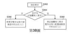
根據本發明的實施例,在一直未命中的情況下,該筆要求最後會被傳送至第N級指令緩衝器330或者寫入配置緩衝器331。第N級指令緩衝器330與寫入配置緩衝器331包括多個入口(entry)可暫存多個要求。寫入配置緩衝器331的入口用來暫存記憶體寫入要求,第N級指令緩衝器330的入口用來暫存其他的要求。也就是說,如第3B圖所示的管理流程圖,第N級接收到該筆要求時(步驟S362),會先判斷該筆要求是否為記憶體寫入要求(步驟S364)。當該筆要求為記憶體寫入要求時,記憶體寫入要求被暫存於寫入配置緩衝器331中的自由入口(步驟S368),而其他要求則被暫存於第N級指令緩衝器330中的自由入口(步驟S366)。According to the embodiment of the present invention, in the case of a miss all the time, the request will be sent to the Nth-
再者,快取裝置370可以任意選擇第N級指令緩衝器330或者寫入配置緩衝器331中多個使用入口(used entry)內的其中一筆要求,並判斷是否命中第N級快取記憶體132。也就是說,第N級指令緩衝器330與寫入配置緩衝器331可各自獨立運作,彼此之間不會互相影響。Moreover, the caching device 370 can arbitrarily select one of the Nth-level instruction buffers 330 or write into the
舉例來說,快取裝置370選擇第N級指令緩衝器330中的一筆要求並判斷命中第N級快取記憶體332時,如果該筆要求為記憶體讀取要求,則第N級快取記憶體332中對應快取線的儲存資料即為讀取資料,並回傳讀取資料至中央處理器350,且該筆記憶體讀取要求被退休(retired),代表該筆記憶體讀取要求已經完成。基本上,快取裝置370對於記憶體讀取要求(memory read request)的管理方式相同於習知管理方式以及第一實施例,所以以下僅介紹 快取裝置370管理記憶體寫入要求的方法。For example, when the cache device 370 selects a request in the Nth-
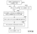
如第3C圖所示的管理流程圖,當快取裝置370選擇寫入配置緩衝器331中的一筆記憶體寫入要求(步驟S372)時,快取裝置370判斷是否命中第N級快取記憶體332(步驟S374)。也就是說,快取裝置370會判斷第N級快取記憶體332的所有快取線內是否記錄相同的位址資訊。如果第N級快取記憶體332的其中一條快取線記錄的位址資訊相同於該筆要求中的位址資訊時,則為命中(hit)。反之,如果第N級快取記憶體332中所有快取線記錄的位址資訊皆異於該筆要求中的位址資訊時,則為未命中(miss)。As shown in the management flowchart of FIG. 3C, when the caching device 370 selects a memory write request written in the configuration buffer 331 (step S372), the caching device 370 judges whether it hits the Nth level cache memory body 332 (step S374). That is to say, the cache device 370 will determine whether the same address information is recorded in all the cache lines of the Nth
於命中(hit)的情況下,快取裝置370執行該筆記憶體寫入要求(步驟S376)。也就是說,快取裝置370將寫入資料更新於第N級快取記憶體332中的對應快取線內,亦即對應快取線中的儲存資料會被更新。接著,該筆記憶體寫入要求被退休(步驟S388),代表該筆記憶體寫入要求已經完成。In case of a hit, the cache device 370 executes the memory write request (step S376). That is to say, the cache device 370 updates the written data in the corresponding cache line in the N-th
於未命中(miss)的情況下,快取裝置370將該筆記憶體寫入要求修改為記憶體讀取要求,並輸出記憶體讀取要求至系統記憶體360(步驟S382)。In the case of a miss, the cache device 370 modifies the memory write request into a memory read request, and outputs the memory read request to the system memory 360 (step S382 ).
根據本發明的實施例,於未命中第N級快取記憶體332的情況下,快取裝置370先將記憶體寫入要求修改為記憶體讀取要求,並輸出記憶體讀取要求至系統記憶體360。之後,系統記憶體360根據記憶體讀取要求產生讀取資料,並回傳至快取裝置370。基本上,對應於此筆讀取資料的記憶體讀取要求並不是由中央處理器350所發出,所以該筆讀取資料不會傳回中央處理器350,僅回傳至快取裝置370。According to an embodiment of the present invention, in the case of a miss in the Nth
再者,於收到系統記憶體360產生的讀取資料時,快取裝置370會將該筆記憶體寫入要求的寫入資料合併(merge)至讀取資料,成為合併資料(merged data)(步驟S384)。接著,將位址資訊與合併資料儲存至快取線(步驟S386)。最後,退休記憶體寫入要求(步驟S388)。Furthermore, when receiving the read data generated by the
根據本發明的實施例,於收到系統記憶體360產生的讀取資料後,快取裝置370會將第N級指令緩衝器330中記憶體寫入要求所對應的寫入資料與讀取資料合併(merge),成為合併資料(merged data)。接著,將記憶體寫入要求中的位址資訊以及合併資料儲存至第N級快取記憶體332中的一條快取線。最後,退休第N級指令緩衝器330中的記憶體寫入要求,代表該筆記憶體寫入要求已完成。According to an embodiment of the present invention, after receiving the read data generated by the
根據本發明的第二實施例,在第3C圖中步驟S382至步驟S384之間會有較長的等待時間。由於本發明快取裝置370的第N級中包括第N級指令緩衝器330與寫入配置緩衝器331。第N級指令緩衝器330與寫入配置緩衝器331可各自獨立運作,彼此之間不會互相影響。因此,在等待時間的過程,快取裝置370仍可以選擇第N級指令緩衝器330內的要求來執行,所以可以維持快取裝置170的運作效能。According to the second embodiment of the present invention, there is a longer waiting time between step S382 and step S384 in FIG. 3C. Since the Nth stage of the cache device 370 of the present invention includes an Nth
另外,由第3B圖的管理流程可知,當記憶體寫入要求被傳送至第N級時,皆會被暫存至寫入配置緩衝器331。也就是說,如果第N級連續接收5筆相同位址資訊的記憶體寫入要求時,該5筆記憶體寫入要求都會被暫存於寫入配置緩衝器331的自由入口。之後,快取裝置370則根據第3C圖的流程來依序執行這5筆記憶體寫入要求。In addition, it can be seen from the management flow in FIG. 3B that when the memory write request is sent to the Nth stage, it will be temporarily stored in the
針對多個相同位址資訊的記憶體寫入要求,本發明更改善第3B圖中記憶體寫入要求暫存至寫入配置緩衝器的方法。使得寫入配置緩衝器可以利用最少的自由入口來暫存多個相同位址資訊的記憶體寫入要求。For multiple memory write requests with the same address information, the present invention further improves the method of temporarily storing the memory write requests to the write configuration buffer in FIG. 3B. The write configuration buffer can use the minimum number of free entries to temporarily store multiple memory write requests with the same address information.
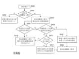
請參照第4圖,其所繪示為記憶體寫入要求暫存至寫入配置緩衝器的另一方法。首先,當第N級接收到一筆要求時(步驟S362),會先判斷該筆要求是否為記憶體寫入要求(步驟S364)。當該筆要求為記憶體寫入要求時,記憶體寫入要求被傳送至寫入配置緩衝器331(步驟S402),而其他要求則被暫存於第N級指令緩衝器330中的自由入口(步驟S366)。Please refer to FIG. 4 , which shows another method for buffering memory write requests to the write configuration buffer. First, when the Nth stage receives a request (step S362), it will first judge whether the request is a memory writing request (step S364). When the request is a memory write request, the memory write request is sent to the write configuration buffer 331 (step S402), while other requests are temporarily stored in the free entry in the Nth-level instruction buffer 330 (step S366).
當一筆記憶體寫入要求傳送至寫入配置緩衝器331時,快取裝置370會先判斷寫入配置緩衝器331中是否有使用入口也記錄相同位址資訊。於確認所有使用入口記錄的位址資訊皆異於該筆記憶體寫入要求的位址資訊,則將該筆記憶體寫入要求暫存至寫入配置緩衝器331中的自由入口(步驟410)。When a memory write request is sent to the
再者,於確認有使用入口記錄的位址資訊相同於該筆記憶體寫入要求的位址資訊時,則進一步判斷是否有多個使用入口記錄的位址資訊相同於該筆記憶體寫入要求的位址資訊(步驟S408)。Furthermore, when it is confirmed that the address information of the use entry record is the same as the address information of the memory write request, it is further judged whether there are multiple use entry records with the same address information as the memory write request. The requested address information (step S408).
於確認有多個使用入口記錄的位址資訊相同於該筆記憶體寫入要求的位址資訊時,將該筆記憶體寫入要求的寫入資料合併至寫入配置緩衝器331內最新(newest)使用者入口的儲存資料(步驟S420)。接著,退休該筆記憶體寫入要求(步驟S422)。在步驟S420中,快取裝置370會在相同位址資訊的多個使用入口之中,決定一個最新使用者入口。然後,將此筆記憶體寫入要求的寫入資料合併至最新使用者入口的儲存資料。When it is confirmed that the address information of multiple usage entry records is the same as the address information of the memory write request, the write data of the memory write request is merged into the
於確認僅有單一使用入口記錄的位址資訊相同於該筆記憶體寫入要求的位址資訊時,再判斷可否將寫入資料合併至寫入配置緩衝器331內對應的使用入口(步驟S412)。When it is confirmed that only the address information of the single use entry record is the same as the address information of the memory write request, then it is judged whether the write data can be merged into the corresponding use entry in the write configuration buffer 331 (step S412 ).
於確認可以合併至對應的使用入口時,將該筆記憶體寫入要求的寫入資料合併至寫入配置緩衝器331中對應的使用者入口的儲存資料(步驟S416)。接著,退休該筆記憶體寫入要求(步驟S422)。When it is confirmed that it can be merged into the corresponding user entry, the write data of the memory write request is merged into the storage data written into the corresponding user entry in the configuration buffer 331 (step S416 ). Next, retire the memory write request (step S422).
於確認不可以合併至對應使用入口時,將該筆記憶體寫入要求暫存至寫入配置緩衝器331中的自由入口(步驟410)。When it is confirmed that it cannot be merged into the corresponding use entry, temporarily store the memory write request to a free entry in the write configuration buffer 331 (step 410 ).
由以上的說明可知,當第N級連續接收多筆相同位址資訊的記憶體寫入要求時,可以適當地將寫入資料合併至使用入口的儲存資料,並退休該筆記憶體寫入要求。因此,第4圖搭配第3C圖的管理方式確實可以減少寫入配置緩衝器331中自由入口的使用數目,更可以提高快取裝置170的運作效能。From the above description, it can be known that when the Nth level continuously receives multiple memory write requests with the same address information, it can properly merge the write data into the storage data of the usage entry, and retire the memory write request . Therefore, the management method in FIG. 4 combined with FIG. 3C can indeed reduce the number of free entries in the
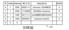
請參照第5A圖至第5F圖,其所繪示為寫入配置緩衝器的管理流程各種範例。如第5A圖所示,寫入配置緩衝器331包括五個入口(entries)。每個入口皆有對應的代碼欄位(ID)、有效欄位(Valid)、位址資訊欄位(Address)、位元組致能欄位(BE[7:0])、資料欄位(Data[63:0])以及忙碌欄位(BUSY)。除此之外,每個入口也可以根據實際需求而增加其他功能的欄位。再者,第5A圖中僅以寫入配置緩衝器331具有五個入口為例來說明,寫入配置緩衝器331也可以有其他數目的入口。Please refer to FIG. 5A to FIG. 5F , which illustrate various examples of management processes for writing configuration buffers. As shown in FIG. 5A, the
在一個入口中,代碼欄位(ID)的數值越小,代表中的記憶體寫入要求暫存於寫入配置緩衝器331的暫存時間越長。也就是說,代碼欄位(ID)的數值0所對應的入口為最舊(oldest)入口,暫存的記憶體寫入要求為最舊的(oldest)的記憶體寫入要求。In an entry, the smaller the value of the code field (ID), the longer the temporary storage time of the memory write request in the representation in the
在一個入口中,有效欄位(Valid)的數值代表對應的入口為自由入口或者是使用入口。如第5A圖所示,代碼欄位(ID)為“0”與“1”入口所對應的有效欄位(Valid)為“1”,代表代碼欄位(ID)為“0”與“1”的入口為使用入口。而其他的入口的有效欄位(Valid)為“0”,代表其他入口為自由入口。In an entry, the value of the valid field (Valid) indicates that the corresponding entry is a free entry or a use entry. As shown in Figure 5A, the code field (ID) is "0" and the valid field (Valid) corresponding to the entry "1" is "1", which means that the code field (ID) is "0" and "1" "The entry is the use entry. The valid field (Valid) of other entries is "0", which means that other entries are free entries.
在一個入口中,位址資訊欄位(Address)的數值為位址資訊,代表記憶體寫入要求欲更新的系統記憶體位址。In an entry, the value of the address information field (Address) is address information, representing the system memory address to be updated by the memory write request.
在一個入口中,位元組致能欄位(BE[7:0])與資料欄位(Data[63:0])互相搭配。其中,位元組致能欄位(BE[7:0])之數值為2進位的數值,資料欄位(Data[63:0])的數值為16進位的數值,而“x”為不理踩數值(don’t care value)。舉例來說,快取記憶體中一條快取線可記錄8位元組(8 bytes)的儲存資料,亦即64位元(64 bits)的儲存資料。因此,寫入配置緩衝器331中每個入口的資料欄位(Data[63:0])內的資料長度(data legth)為64位元(64 bits)。再者,位元組致能欄位(BE[7:0])代表欲更新寫入資料位置。In an entry, the byte enable field (BE[7:0]) is paired with the data field (Data[63:0]). Among them, the value of the byte enable field (BE[7:0]) is a binary value, the value of the data field (Data[63:0]) is a hexadecimal value, and "x" is not Don't care value. For example, a cache line in the cache memory can record 8 bytes (8 bytes) of storage data, that is, 64 bits (64 bits) of storage data. Therefore, the data length (data leg) written into the data field (Data[63:0]) of each entry in the
以代碼欄位(ID)為“0”的使用入口為例來說明,該使用入口暫存一第一記憶體寫入要求,其位元組致能欄位(BE[7:0])為“00001111”,代表第一記憶體寫入要求僅更新8個位元組中的後4個位元組。亦即,寫入資料為四位元組,依序為“12”、“34”、“AB”、“CD”。Take the use entry whose code field (ID) is "0" as an example to illustrate. This use entry temporarily stores a first memory write request, and its byte enabling field (BE[7:0]) is "00001111" means that the first memory write request only updates the last 4 bytes among the 8 bytes. That is, the written data is four bytes, which are "12", "34", "AB", and "CD" in sequence.
同理,代碼欄位(ID)為“1”的使用入口暫存一第二記憶體寫入要求,其位元組致能欄位(BE[7:0])為“11100000”,代表第二記憶體寫入要求僅更新8個位元組中的前3個位元組。亦即,寫入資料為三位元組,依序為“56”、“78”、“90”。Similarly, the use entry whose code field (ID) is "1" temporarily stores a second memory write request, and its byte enable field (BE[7:0]) is "11100000", representing the second memory write request. Two memory writes require only the first 3 bytes of the 8 bytes to be updated. That is, the written data is three bytes, which are "56", "78", and "90" in sequence.
在一個入口中,忙碌欄位(BUSY),代表該使用入口是否正在執行中。舉例來說,當忙碌欄位(BUSY)設定為“0”代表該使用入口的記憶體寫入要求尚未被選擇。此時,對應的該使用入口內的儲存資料可以被合併。反之,當快取裝置370選擇並判斷第一記憶體寫入要求是否命中第N級快取記憶體332時,該使用入口的忙碌欄位(BUSY)會被設定為“1”。此時,對應的該使用入口內的儲存資料不可以被合併。。In an entry, the busy field (BUSY) indicates whether the use entry is being executed. For example, when the busy field (BUSY) is set to "0", it means that the memory write request of the usage entry has not been selected yet. At this time, the stored data in the corresponding usage entry can be merged. On the contrary, when the cache device 370 selects and determines whether the first memory write request hits the Nth
在第5A圖的情況下。當快取裝置370的第N級接收到一第三記憶體寫入要求,且第三記憶體寫入要求的位址資訊(Address)為 “1000”,位元組致能欄位(BE[7:0])數值為“00001111”, 資料欄位(Data[63:0])的數值為 “xxxxxxxx AAAAAAAA”。In the case of Figure 5A. When the Nth stage of the cache device 370 receives a third memory write request, and the address information (Address) of the third memory write request is "1000", the byte enable field (BE[ 7:0]) is "00001111", and the data field (Data[63:0]) is "xxxxxxxx AAAAAAA".
此時,快取裝置370判斷寫入配置緩衝器331中沒有使用入口也記錄“1000”的位址資訊(Addrss)。由於所有使用入口記錄的位址資訊(Addrsss)皆異於第三記憶體寫入要求的位址資訊(Address)“1000”。因此,如第5B圖所示,快取裝置370將第三記憶體寫入要求暫存至寫入配置緩衝器331中的編號( ID)2的自由入口。也就是說,經由步驟(S362)、步驟(S364)、步驟(S402)、步驟(S406)、步驟(S410)後,第三記憶體寫入要求被暫存至編號( ID)2的自由入口。At this time, the cache device 370 judges that the address information (Addrss) of “1000” is also recorded in the
在第5B圖的情況下。當快取裝置370的第N級接收到一第四記憶體寫入要求,且第四記憶體寫入要求的位址資訊(Address)為 “1000”,位元組致能欄位(BE[7:0])數值為“00111000”, 資料欄位(Data[63:0])的數值為 “xxxxBBBB BBxxxxxx”。In the case of Figure 5B. When the Nth stage of the cache device 370 receives a fourth memory write request, and the address information (Address) of the fourth memory write request is "1000", the byte enable field (BE[ 7:0]) is "00111000", and the data field (Data[63:0]) is "xxxxBBBB BBxxxxxx".
此時,快取裝置370判斷寫入配置緩衝器331中有使用入口也記錄“1000”的位址資訊(Addrss)。由於使用入口代碼欄位(ID)“2”內記錄的位址資訊(Addrsss)為“1000”,且忙碌欄位(BUSY)為“0”。因此,如第5C圖所示,快取裝置370將第四記憶體寫入要求的寫入資料合併至使用入口代碼欄位(ID)“2”內的儲存資料。在第5C圖中,位元組致能欄位(BE[7:0])數值修改為“00111111”, 資料欄位(Data[63:0])的數值合併為 “xxxxBBBB BBAAAAAA”。之後,該第四記憶體寫入要求被退休。也就是說,經由步驟(S362)、步驟(S364)、步驟(S402)、步驟(S406)、步驟(S408) 、步驟(S412)、步驟(S416)後,第四記憶體寫入要求的寫入資料與第三寫入要求的寫入資料合併,第四記憶體寫入要求不會被暫存至自由入口,且第四記憶體寫入要求會被退休。At this time, the cache device 370 determines that there is an address information (Addrss) of “1000” recorded in the
在第5C圖的情況下,當快取裝置370選擇使用入口代碼欄位(ID)“2”內的記憶體寫入要求並判斷是否命中第N級快取記憶體332時,如第 5D圖所示,對應使用入口的忙碌欄位(BUSY)為“1”。In the case of Figure 5C, when the cache device 370 chooses to use the memory write request in the entry code column (ID) "2" and judges whether it hits the Nth
在第5D圖的情況下。當快取裝置370的第N級接收到一第五記憶體寫入要求,且第五記憶體寫入要求的位址資訊(Address)為 “1000”,位元組致能欄位(BE[7:0])數值為“00000011”, 資料欄位(Data[63:0])的數值為 “xxxxxxxx xxxxCCCC”。In the case of Fig. 5D. When the Nth stage of the cache device 370 receives a fifth memory write request, and the address information (Address) of the fifth memory write request is "1000", the byte enable field (BE[ 7:0]) is "00000011", and the data field (Data[63:0]) is "xxxxxxxx xxxxCCCC".
此時,快取裝置370判斷寫入配置緩衝器331中雖然有使用入口也記錄“1000”的位址資訊(Addrss)。但是,由於使用入口代碼欄位(ID)“2”內記錄的位址資訊(Addrsss)為“1000”,且忙碌欄位(BUSY)為“1”。因此,如第5E圖所示,快取裝置370無法合併寫入資料。因此,如第5E圖所示,快取裝置370將第五記憶體寫入要求暫存至寫入配置緩衝器331中的編號( ID)3的自由入口。也就是說,經由步驟(S362)、步驟(S364)、步驟(S402)、步驟(S406)、步驟(S410)後,第五記憶體寫入要求被暫存至編號( ID)3的自由入口。此時,有二個相同位址資訊的記憶體寫入要求暫存於寫入配置緩衝器331中。At this time, the cache device 370 judges that the address information (Addrss) of “1000” is recorded in the
在第5E圖的情況下。當快取裝置370的第N級接收到一第六記憶體寫入要求,且第六記憶體寫入要求的位址資訊(Address)為 “1000”,位元組致能欄位(BE[7:0])數值為“11111111”, 資料欄位(Data[63:0])的數值為 “08090A0B0C0D0E0F”。In the case of Fig. 5E. When the Nth stage of the cache device 370 receives a sixth memory write request, and the address information (Address) of the sixth memory write request is "1000", the byte enable field (BE[ 7:0]) is "11111111", and the data field (Data[63:0]) is "08090A0B0C0D0E0F".
此時,快取裝置370判斷寫入配置緩衝器331有使用入口也記錄“1000”的位址資訊(Addrss)。由於使用入口代碼欄位(ID)“2”與“3”內記錄的位址資訊(Addrsss)皆為“1000”。因此,如第5F圖所示,快取裝置370將第六記憶體寫入要求的寫入資料合併至最新(newest)使用入口代碼欄位(ID)“3”內的儲存資料。在第5F圖中,位元組致能欄位(BE[7:0])數值修改為“11111111”, 資料欄位(Data[63:0])的數值合併為 “08090A0B0C0D0E0F”。之後,該第六記憶體寫入要求被退休。也就是說,經由步驟(S362)、步驟(S364)、步驟(S402)、步驟(S406)、步驟(S408) 、步驟(S420)、步驟(S422)後,第六記憶體寫入要求的寫入資料與第五寫入要求的寫入資料合併,第六記憶體寫入要求不會被暫存至自由入口,且第六記憶體寫入要求會被退休。At this time, the cache device 370 determines that there is an address information (Addrss) of “1000” recorded in the use entry in the
另外,在第5D圖的情況下,對應使用入口的忙碌欄位(BUSY)為“1”。代表快取裝置370正選擇使用入口代碼欄位(ID)“2”內的記憶體寫入要求並判斷是否命中第N級快取記憶體332。當快取裝置370判斷記憶體寫入要求並未命中第N級快取記憶體332時,該筆記憶體寫入要求會被修改為記憶體讀取要求並被傳送至系統記憶體360。此時,將會有一段等待時間,等待系統記憶體360回傳讀取資料。而在等待時間的過程,入口代碼欄位(ID)“2”的忙碌欄位(BUSY)會被改為“0”。因此,如果在等待時間內,快取裝置370的第N級接收到一第七記憶體寫入要求,且第七記憶體寫入要求的位址資訊(Address)為 “1000”,則第七記憶體寫入要求中的寫入資料也可以合併至入口代碼欄位(ID)“2”使用入口的儲存資料。In addition, in the case of FIG. 5D, the busy field (BUSY) of the corresponding usage entry is "1". It means that the cache device 370 is selecting to use the memory write request in the entry code field (ID) “2” and judging whether it hits the Nth
由以上的說明可知,本發明提出一種快取裝置中管理記憶體寫入要求的方法。在快取裝置370的第N級中更增加了一寫入配置緩衝器331,寫入配置緩衝器331僅能暫存記憶體寫入要求。由於第N級指令緩衝器330與寫入配置緩衝器331可各自獨立運作,彼此之間不會互相影響,所以可以維持快取裝置170的運作效能。另外,本發明更提出另一種寫入配置緩衝器331的管理方式,可以適當地將寫入資料合併至使用入口的儲存資料,降低寫入配置緩衝器331使用自由入口的數目。As can be seen from the above description, the present invention provides a method for managing memory write requests in a cache device. A
另外,在上述的說明中,皆假設第N級為快取裝置370的最後一級,且寫入配置緩衝器331則增加在第N級。然而,本發明並不限定於此,本發明的寫入配置緩衝器331也可以不用增加在最後一級(level)。舉例來說,快取裝置370中有P級(level),且P為大於2的整數。再者,且N為大於1小於P的整數,且寫入配置緩衝器331增加在第N級。如此,在寫入配置緩衝器331不是增加在最後一級的情況下,也能夠達成本發明的目的。In addition, in the above description, it is assumed that the Nth stage is the last stage of the cache device 370, and the
綜上所述,雖然本發明已以較佳實施例揭露如上,然其並非用以限定本發明。本發明所屬技術領域中具有通常知識者,在不脫離本發明之精神和範圍內,當可作各種之更動與潤飾。因此,本發明之保護範圍當視後附之申請專利範圍所界定者為準。To sum up, although the present invention has been disclosed as above with preferred embodiments, it is not intended to limit the present invention. Those skilled in the art of the present invention can make various changes and modifications without departing from the spirit and scope of the present invention. Therefore, the scope of protection of the present invention should be defined by the scope of the appended patent application.
112,312:第一級快取記憶體 129,320:第二級指令緩衝器 122,322:第二級快取記憶體 130,330:第N級指令緩衝器 132,332:第N級快取記憶體 150,350:中央處理器 160,360:系統記憶體 170,370:快取裝置 331:寫入配置緩衝器 S272~S422:步驟流程112,312:
第1圖為習知電腦系統中的快取裝置示意圖; 第2圖為電腦系統中快取裝置管理記憶體寫入要求的方法第一實施例; 第3A圖為本明電腦系統中的快取裝置示意圖; 第3B圖為管理記憶體寫入要求暫存至寫入配置緩衝器的方法; 第3C圖為本發明快取裝置中執行記憶體寫入要求的方法; 第4圖為記憶體寫入要求暫存至寫入配置緩衝器的另一方法;以及 第5A圖至第5F圖為寫入配置緩衝器的管理流程各種範例。Fig. 1 is a schematic diagram of a cache device in a conventional computer system; The 2nd figure is the first embodiment of the method for caching device management memory writing requirements in the computer system; Figure 3A is a schematic diagram of the cache device in the computer system of the present invention; FIG. 3B is a method for managing memory write requests temporarily stored in a write configuration buffer; Fig. 3C is a method for executing memory writing requirements in the cache device of the present invention; FIG. 4 is another method for buffering memory write requests to write configuration buffers; and FIG. 5A to FIG. 5F illustrate various examples of management processes for writing configuration buffers.
312:第一級快取記憶體312:
320:第二級指令緩衝器320: Second level instruction buffer
322:第二級快取記憶體322:Second level cache memory
330:第N級指令緩衝器330: Nth-level instruction buffer
331:寫入配置緩衝器331: Write configuration buffer
332:第N級快取記憶體332: Level N cache memory
350:中央處理器350: CPU
360:系統記憶體360: System memory
370:快取裝置370: cache device
Claims (13)
Translated fromChinesePriority Applications (2)
| Application Number | Priority Date | Filing Date | Title |
|---|---|---|---|
| TW111142793ATWI811151B (en) | 2022-11-09 | 2022-11-09 | Method for managing memory write request in cache device |
| US18/113,307US20240152459A1 (en) | 2022-11-09 | 2023-02-23 | Method for managing memory write request in cache device |
Applications Claiming Priority (1)
| Application Number | Priority Date | Filing Date | Title |
|---|---|---|---|
| TW111142793ATWI811151B (en) | 2022-11-09 | 2022-11-09 | Method for managing memory write request in cache device |
Publications (2)
| Publication Number | Publication Date |
|---|---|
| TWI811151Btrue TWI811151B (en) | 2023-08-01 |
| TW202420101A TW202420101A (en) | 2024-05-16 |
Family
ID=88585473
Family Applications (1)
| Application Number | Title | Priority Date | Filing Date |
|---|---|---|---|
| TW111142793ATWI811151B (en) | 2022-11-09 | 2022-11-09 | Method for managing memory write request in cache device |
Country Status (2)
| Country | Link |
|---|---|
| US (1) | US20240152459A1 (en) |
| TW (1) | TWI811151B (en) |
Citations (5)
| Publication number | Priority date | Publication date | Assignee | Title |
|---|---|---|---|---|
| TW378293B (en)* | 1995-12-27 | 2000-01-01 | Intel Corporaiton | Method and apparatus for combining multiple writes to a memory |
| CN113853652A (en)* | 2019-05-24 | 2021-12-28 | 德州仪器公司 | Pipelined read-modify-write operations in a cache |
| TW202211021A (en)* | 2020-09-02 | 2022-03-16 | 美商賽發馥股份有限公司 | Method for executing atomic memory operations when contested |
| US20220164217A1 (en)* | 2019-05-24 | 2022-05-26 | Texas Instruments Incorporated | Merging data for write allocate |
| US20220327055A1 (en)* | 2019-05-24 | 2022-10-13 | Texas Instruments Incorporated | Aliased mode for cache controller |
Family Cites Families (9)
| Publication number | Priority date | Publication date | Assignee | Title |
|---|---|---|---|---|
| US6430654B1 (en)* | 1998-01-21 | 2002-08-06 | Sun Microsystems, Inc. | Apparatus and method for distributed non-blocking multi-level cache |
| US6519682B2 (en)* | 1998-12-04 | 2003-02-11 | Stmicroelectronics, Inc. | Pipelined non-blocking level two cache system with inherent transaction collision-avoidance |
| US8219379B2 (en)* | 2004-11-29 | 2012-07-10 | Arm Limited | System, method and computer program product for testing software |
| US20110213998A1 (en)* | 2008-06-11 | 2011-09-01 | John George Mathieson | System and Method for Power Optimization |
| CN101876944B (en)* | 2009-11-26 | 2012-02-15 | 威盛电子股份有限公司 | Dynamic random access memory controller and control method |
| JPWO2013014841A1 (en)* | 2011-07-22 | 2015-02-23 | パナソニック株式会社 | Data processing apparatus and data processing method |
| US8788788B2 (en)* | 2011-08-11 | 2014-07-22 | Pure Storage, Inc. | Logical sector mapping in a flash storage array |
| US9235521B2 (en)* | 2013-07-22 | 2016-01-12 | Avago Technologies General Ip (Singapore) Pte Ltd | Cache system for managing various cache line conditions |
| US11513962B2 (en)* | 2020-10-13 | 2022-11-29 | Arm Limited | Draining operation to cause store data to be written to persistent memory |
- 2022
- 2022-11-09TWTW111142793Apatent/TWI811151B/enactive
- 2023
- 2023-02-23USUS18/113,307patent/US20240152459A1/ennot_activeAbandoned
Patent Citations (5)
| Publication number | Priority date | Publication date | Assignee | Title |
|---|---|---|---|---|
| TW378293B (en)* | 1995-12-27 | 2000-01-01 | Intel Corporaiton | Method and apparatus for combining multiple writes to a memory |
| CN113853652A (en)* | 2019-05-24 | 2021-12-28 | 德州仪器公司 | Pipelined read-modify-write operations in a cache |
| US20220164217A1 (en)* | 2019-05-24 | 2022-05-26 | Texas Instruments Incorporated | Merging data for write allocate |
| US20220327055A1 (en)* | 2019-05-24 | 2022-10-13 | Texas Instruments Incorporated | Aliased mode for cache controller |
| TW202211021A (en)* | 2020-09-02 | 2022-03-16 | 美商賽發馥股份有限公司 | Method for executing atomic memory operations when contested |
Also Published As
| Publication number | Publication date |
|---|---|
| TW202420101A (en) | 2024-05-16 |
| US20240152459A1 (en) | 2024-05-09 |
Similar Documents
| Publication | Publication Date | Title |
|---|---|---|
| JP3620473B2 (en) | Method and apparatus for controlling replacement of shared cache memory | |
| US9442846B2 (en) | High speed memory systems and methods for designing hierarchical memory systems | |
| US8799585B2 (en) | Cache memory capable of adjusting burst length of write-back data in write-back operation | |
| CN112527395B (en) | Data prefetching method and data processing apparatus | |
| US8621152B1 (en) | Transparent level 2 cache that uses independent tag and valid random access memory arrays for cache access | |
| TW200805061A (en) | Patrol snooping for higher level cache eviction candidate identification | |
| TWI588831B (en) | Non-volatile memory accelerator and method for speed up data accessing thereof | |
| CN115168248A (en) | Cache memory and corresponding processor supporting SIMT architecture | |
| CN115605849A (en) | Kernel cache hiding and target discovery | |
| CN107506139A (en) | A kind of write request towards phase transition storage optimizes device | |
| JP3407808B2 (en) | Computer system | |
| CN115098409B (en) | Processor and method for performing hierarchical cache system restore and invalidation | |
| JP2004199677A (en) | System for and method of operating cache | |
| US7949833B1 (en) | Transparent level 2 cache controller | |
| TWI811151B (en) | Method for managing memory write request in cache device | |
| JP2019200473A (en) | Memory control apparatus, memory control program, and memory control method | |
| WO2024198789A1 (en) | Method for gpu, and gpu | |
| CN114283048B (en) | Cache memory applied to three-dimensional graphics depth test | |
| TWI742770B (en) | Neural network computing device and cache management method thereof | |
| JP2004240616A (en) | Memory controller and memory access control method | |
| CN116830092A (en) | Techniques for tracking modifications to the contents of a memory area | |
| US7421536B2 (en) | Access control method, disk control unit and storage apparatus | |
| CN115686349A (en) | Storage system for maintaining data consistency and operation method thereof | |
| CN101419543A (en) | Method and system for predicting access position of high-speed register | |
| JP3006204B2 (en) | Information processing device |