TWI803495B - Methods for forming semiconductor device structures - Google Patents
Methods for forming semiconductor device structuresDownload PDFInfo
- Publication number
- TWI803495B TWI803495BTW107117734ATW107117734ATWI803495BTW I803495 BTWI803495 BTW I803495BTW 107117734 ATW107117734 ATW 107117734ATW 107117734 ATW107117734 ATW 107117734ATW I803495 BTWI803495 BTW I803495B
- Authority
- TW
- Taiwan
- Prior art keywords
- mask layer
- layer
- trench
- groove
- mask
- Prior art date
Links
Images


Classifications
- H—ELECTRICITY
- H01—ELECTRIC ELEMENTS
- H01L—SEMICONDUCTOR DEVICES NOT COVERED BY CLASS H10
- H01L23/00—Details of semiconductor or other solid state devices
- H01L23/52—Arrangements for conducting electric current within the device in operation from one component to another, i.e. interconnections, e.g. wires, lead frames
- H01L23/538—Arrangements for conducting electric current within the device in operation from one component to another, i.e. interconnections, e.g. wires, lead frames the interconnection structure between a plurality of semiconductor chips being formed on, or in, insulating substrates
- H01L23/5386—Geometry or layout of the interconnection structure
- H—ELECTRICITY
- H01—ELECTRIC ELEMENTS
- H01L—SEMICONDUCTOR DEVICES NOT COVERED BY CLASS H10
- H01L21/00—Processes or apparatus adapted for the manufacture or treatment of semiconductor or solid state devices or of parts thereof
- H01L21/70—Manufacture or treatment of devices consisting of a plurality of solid state components formed in or on a common substrate or of parts thereof; Manufacture of integrated circuit devices or of parts thereof
- H01L21/71—Manufacture of specific parts of devices defined in group H01L21/70
- H01L21/768—Applying interconnections to be used for carrying current between separate components within a device comprising conductors and dielectrics
- H01L21/76838—Applying interconnections to be used for carrying current between separate components within a device comprising conductors and dielectrics characterised by the formation and the after-treatment of the conductors
- H01L21/76841—Barrier, adhesion or liner layers
- H01L21/76843—Barrier, adhesion or liner layers formed in openings in a dielectric
- H—ELECTRICITY
- H01—ELECTRIC ELEMENTS
- H01L—SEMICONDUCTOR DEVICES NOT COVERED BY CLASS H10
- H01L21/00—Processes or apparatus adapted for the manufacture or treatment of semiconductor or solid state devices or of parts thereof
- H01L21/02—Manufacture or treatment of semiconductor devices or of parts thereof
- H01L21/04—Manufacture or treatment of semiconductor devices or of parts thereof the devices having potential barriers, e.g. a PN junction, depletion layer or carrier concentration layer
- H01L21/50—Assembly of semiconductor devices using processes or apparatus not provided for in a single one of the groups H01L21/18 - H01L21/326 or H10D48/04 - H10D48/07 e.g. sealing of a cap to a base of a container
- H—ELECTRICITY
- H01—ELECTRIC ELEMENTS
- H01L—SEMICONDUCTOR DEVICES NOT COVERED BY CLASS H10
- H01L21/00—Processes or apparatus adapted for the manufacture or treatment of semiconductor or solid state devices or of parts thereof
- H01L21/70—Manufacture or treatment of devices consisting of a plurality of solid state components formed in or on a common substrate or of parts thereof; Manufacture of integrated circuit devices or of parts thereof
- H01L21/71—Manufacture of specific parts of devices defined in group H01L21/70
- H01L21/76—Making of isolation regions between components
- H01L21/762—Dielectric regions, e.g. EPIC dielectric isolation, LOCOS; Trench refilling techniques, SOI technology, use of channel stoppers
- H—ELECTRICITY
- H01—ELECTRIC ELEMENTS
- H01L—SEMICONDUCTOR DEVICES NOT COVERED BY CLASS H10
- H01L21/00—Processes or apparatus adapted for the manufacture or treatment of semiconductor or solid state devices or of parts thereof
- H01L21/70—Manufacture or treatment of devices consisting of a plurality of solid state components formed in or on a common substrate or of parts thereof; Manufacture of integrated circuit devices or of parts thereof
- H01L21/71—Manufacture of specific parts of devices defined in group H01L21/70
- H01L21/768—Applying interconnections to be used for carrying current between separate components within a device comprising conductors and dielectrics
- H01L21/76801—Applying interconnections to be used for carrying current between separate components within a device comprising conductors and dielectrics characterised by the formation and the after-treatment of the dielectrics, e.g. smoothing
- H01L21/76802—Applying interconnections to be used for carrying current between separate components within a device comprising conductors and dielectrics characterised by the formation and the after-treatment of the dielectrics, e.g. smoothing by forming openings in dielectrics
- H01L21/76807—Applying interconnections to be used for carrying current between separate components within a device comprising conductors and dielectrics characterised by the formation and the after-treatment of the dielectrics, e.g. smoothing by forming openings in dielectrics for dual damascene structures
- H01L21/76811—Applying interconnections to be used for carrying current between separate components within a device comprising conductors and dielectrics characterised by the formation and the after-treatment of the dielectrics, e.g. smoothing by forming openings in dielectrics for dual damascene structures involving multiple stacked pre-patterned masks
- H—ELECTRICITY
- H01—ELECTRIC ELEMENTS
- H01L—SEMICONDUCTOR DEVICES NOT COVERED BY CLASS H10
- H01L21/00—Processes or apparatus adapted for the manufacture or treatment of semiconductor or solid state devices or of parts thereof
- H01L21/70—Manufacture or treatment of devices consisting of a plurality of solid state components formed in or on a common substrate or of parts thereof; Manufacture of integrated circuit devices or of parts thereof
- H01L21/71—Manufacture of specific parts of devices defined in group H01L21/70
- H01L21/768—Applying interconnections to be used for carrying current between separate components within a device comprising conductors and dielectrics
- H01L21/76838—Applying interconnections to be used for carrying current between separate components within a device comprising conductors and dielectrics characterised by the formation and the after-treatment of the conductors
- H01L21/76877—Filling of holes, grooves or trenches, e.g. vias, with conductive material
- H—ELECTRICITY
- H01—ELECTRIC ELEMENTS
- H01L—SEMICONDUCTOR DEVICES NOT COVERED BY CLASS H10
- H01L23/00—Details of semiconductor or other solid state devices
- H01L23/48—Arrangements for conducting electric current to or from the solid state body in operation, e.g. leads, terminal arrangements ; Selection of materials therefor
- H01L23/481—Internal lead connections, e.g. via connections, feedthrough structures
- H—ELECTRICITY
- H01—ELECTRIC ELEMENTS
- H01L—SEMICONDUCTOR DEVICES NOT COVERED BY CLASS H10
- H01L23/00—Details of semiconductor or other solid state devices
- H01L23/52—Arrangements for conducting electric current within the device in operation from one component to another, i.e. interconnections, e.g. wires, lead frames
- H01L23/522—Arrangements for conducting electric current within the device in operation from one component to another, i.e. interconnections, e.g. wires, lead frames including external interconnections consisting of a multilayer structure of conductive and insulating layers inseparably formed on the semiconductor body
- H01L23/5226—Via connections in a multilevel interconnection structure
- H—ELECTRICITY
- H01—ELECTRIC ELEMENTS
- H01L—SEMICONDUCTOR DEVICES NOT COVERED BY CLASS H10
- H01L23/00—Details of semiconductor or other solid state devices
- H01L23/52—Arrangements for conducting electric current within the device in operation from one component to another, i.e. interconnections, e.g. wires, lead frames
- H01L23/538—Arrangements for conducting electric current within the device in operation from one component to another, i.e. interconnections, e.g. wires, lead frames the interconnection structure between a plurality of semiconductor chips being formed on, or in, insulating substrates
- H01L23/5384—Conductive vias through the substrate with or without pins, e.g. buried coaxial conductors
- H—ELECTRICITY
- H01—ELECTRIC ELEMENTS
- H01L—SEMICONDUCTOR DEVICES NOT COVERED BY CLASS H10
- H01L24/00—Arrangements for connecting or disconnecting semiconductor or solid-state bodies; Methods or apparatus related thereto
- H01L24/01—Means for bonding being attached to, or being formed on, the surface to be connected, e.g. chip-to-package, die-attach, "first-level" interconnects; Manufacturing methods related thereto
- H01L24/18—High density interconnect [HDI] connectors; Manufacturing methods related thereto
- H01L24/19—Manufacturing methods of high density interconnect preforms
- H—ELECTRICITY
- H01—ELECTRIC ELEMENTS
- H01L—SEMICONDUCTOR DEVICES NOT COVERED BY CLASS H10
- H01L24/00—Arrangements for connecting or disconnecting semiconductor or solid-state bodies; Methods or apparatus related thereto
- H01L24/01—Means for bonding being attached to, or being formed on, the surface to be connected, e.g. chip-to-package, die-attach, "first-level" interconnects; Manufacturing methods related thereto
- H01L24/18—High density interconnect [HDI] connectors; Manufacturing methods related thereto
- H01L24/20—Structure, shape, material or disposition of high density interconnect preforms
Landscapes
- Engineering & Computer Science (AREA)
- Computer Hardware Design (AREA)
- Microelectronics & Electronic Packaging (AREA)
- Power Engineering (AREA)
- Physics & Mathematics (AREA)
- Condensed Matter Physics & Semiconductors (AREA)
- General Physics & Mathematics (AREA)
- Manufacturing & Machinery (AREA)
- Geometry (AREA)
- Internal Circuitry In Semiconductor Integrated Circuit Devices (AREA)
- Recrystallisation Techniques (AREA)
Abstract
Description
Translated fromChinese本發明實施例係有關於半導體技術,且特別是有關於半導體裝置結構的形成方法。Embodiments of the present invention relate to semiconductor technology, and more particularly to methods of forming semiconductor device structures.
半導體積體電路(integrated circuit,IC)工業已經歷了快速成長。在積體電路材料和設計上的技術進步產生了數代積體電路,每一代都比前一代具有更小且更複雜的電路。然而,這些進步增加了加工與製造積體電路的複雜性。The semiconductor integrated circuit (IC) industry has experienced rapid growth. Technological advances in integrated circuit materials and design have produced generations of integrated circuits, each with smaller and more complex circuits than the previous generation. However, these advances have increased the complexity of processing and manufacturing integrated circuits.
在積體電路的發展史中,功能密度(即每一晶片區互連的裝置數目)增加,同時幾何尺寸(即製造過程中所產生的最小的組件(或線路))縮小。此元件尺寸微縮化的製程一般來說具有增加生產效率與降低相關費用的益處。In the history of integrated circuits, functional density (ie, the number of devices interconnected per die area) has increased while geometry size (ie, the smallest component (or circuit) produced during fabrication) has shrunk. This process of device size miniaturization generally has the benefits of increasing production efficiency and reducing related costs.
然而,由於部件(feature)尺寸持續縮減,製造製程持續變的更加難以實施。因此,形成越來越小的尺寸的可靠的半導體裝置是個挑戰。However, as feature sizes continue to shrink, manufacturing processes continue to become more difficult to implement. Therefore, forming reliable semiconductor devices of smaller and smaller dimensions is a challenge.
在一些實施例中,提供半導體裝置結構的形成方法,此方法包含在介電層上方形成第一遮罩層,其中第一遮罩層具有第一溝槽,且第一溝槽具有內壁和底表面;在第一溝槽 中形成第二遮罩層;移除覆蓋底表面的第二遮罩層,以在第二遮罩層中形成第二溝槽,其中第二溝槽暴露出底表面且在介電層的第一部分上方,且留下的第二遮罩層覆蓋內壁;移除第一部分、第一遮罩層和第二遮罩層,以在介電層中形成第三溝槽;以及在第三溝槽中形成導電結構。In some embodiments, a method for forming a semiconductor device structure is provided. The method includes forming a first mask layer over a dielectric layer, wherein the first mask layer has a first trench, and the first trench has inner walls and bottom surface; forming a second mask layer in the first trench; removing the second mask layer covering the bottom surface to form a second trench in the second mask layer, wherein the second trench exposes the bottom surface and above the first portion of the dielectric layer, and a second mask layer is left covering the inner wall; the first portion, the first mask layer, and the second mask layer are removed to form a third mask layer in the dielectric layer a trench; and forming a conductive structure in the third trench.
在一些其他實施例中,提供半導體裝置結構的形成方法,此方法包含在介電層上方形成第一遮罩層,其中第一遮罩層具有第一溝槽和第二溝槽,且第一溝槽具有第一內壁和第一底表面;在第一內壁上方順應性形成第二遮罩層,其中第二遮罩層具有在第一溝槽中的第三溝槽並暴露出第一底表面,第三溝槽比第二溝槽窄,且第三溝槽和第二溝槽分別在介電層的第一部分和第二部分上方;移除第一部分、第二部分、第一遮罩層和第二遮罩層,以在介電層中形成第四溝槽和第五溝槽,其中第四溝槽比第五溝槽窄;以及分別在第四溝槽和第五溝槽中形成第一導電結構和第二導電結構。In some other embodiments, a method of forming a semiconductor device structure is provided, the method comprising forming a first mask layer over a dielectric layer, wherein the first mask layer has a first trench and a second trench, and the first The groove has a first inner wall and a first bottom surface; a second mask layer is conformably formed over the first inner wall, wherein the second mask layer has a third groove in the first groove and exposes the first groove. A bottom surface, the third groove is narrower than the second groove, and the third groove and the second groove are respectively above the first part and the second part of the dielectric layer; remove the first part, the second part, the first a mask layer and a second mask layer to form fourth trenches and fifth trenches in the dielectric layer, wherein the fourth trenches are narrower than the fifth trenches; A first conductive structure and a second conductive structure are formed in the groove.
在一些其他實施例中,提供半導體裝置結構的形成方法,此方法包含在介電層上方形成第一遮罩層,其中第一遮罩層具有第一溝槽和第二溝槽,且第一溝槽具有第一內壁和第一底表面;在第一遮罩層的頂表面和第一內壁上方形成第二遮罩層,其中在第一內壁上方的第二遮罩層的厚度沿遠離介電層的方向增加,第二遮罩層具有在第一溝槽中的第三溝槽並暴露出第一底表面,且第三溝槽和第二溝槽分別在介電層的第一部分和第二部分上方;移除第一部分、第二部分、第一遮罩層和第二遮罩層,以在介電層中形成第四溝槽和第五溝槽,其中 第四溝槽比第五溝槽窄;以及分別在第四溝槽和第五溝槽中形成第一導電結構和第二導電結構。In some other embodiments, a method of forming a semiconductor device structure is provided, the method comprising forming a first mask layer over a dielectric layer, wherein the first mask layer has a first trench and a second trench, and the first The trench has a first inner wall and a first bottom surface; a second mask layer is formed over the top surface of the first mask layer and the first inner wall, wherein the thickness of the second mask layer above the first inner wall is increasing along the direction away from the dielectric layer, the second mask layer has a third groove in the first groove and exposes the first bottom surface, and the third groove and the second groove are respectively in the dielectric layer Above the first part and the second part; remove the first part, the second part, the first mask layer and the second mask layer to form a fourth trench and a fifth trench in the dielectric layer, wherein the fourth trench The groove is narrower than the fifth trench; and the first conductive structure and the second conductive structure are formed in the fourth trench and the fifth trench, respectively.
110‧‧‧半導體基底110‧‧‧Semiconductor substrate
110A、110B‧‧‧區域110A, 110B‧‧‧area
120‧‧‧介電層120‧‧‧dielectric layer
122、155、S1、S2、S3、S4‧‧‧頂表面122, 155, S1, S2, S3, S4‧‧‧top surface
130、150、220、310‧‧‧遮罩層130, 150, 220, 310‧‧‧Mask layer
140‧‧‧硬遮罩層140‧‧‧hard mask layer
151、152、153、154、182、212、222、224、226、228、312、314、316、318、R1、R2、R3、R4‧‧‧溝槽151, 152, 153, 154, 182, 212, 222, 224, 226, 228, 312, 314, 316, 318, R1, R2, R3, R4‧‧‧groove
160、190‧‧‧下層160, 190‧‧‧lower floor
170、200‧‧‧中間層170, 200‧‧‧intermediate layer
180、210‧‧‧上層180, 210‧‧‧upper floor
222a、224a、226a、228a、N1、N2、N3、N4‧‧‧內壁222a, 224a, 226a, 228a, N1, N2, N3, N4‧‧‧inner wall
229‧‧‧側壁229‧‧‧side wall
230‧‧‧光阻層230‧‧‧photoresist layer
240‧‧‧阻障層240‧‧‧barrier layer
250‧‧‧導電材料層250‧‧‧conductive material layer
B1、B2、B3、B4‧‧‧底表面B1, B2, B3, B4‧‧‧bottom surface
D1、D2‧‧‧距離D1, D2‧‧‧distance
L1、L2、L3、L4‧‧‧導電結構L1, L2, L3, L4‧‧‧conductive structure
M1、M2‧‧‧圖案化的遮罩結構M1, M2‧‧‧patterned mask structure
T1、T2、T3、T4、T4’、T5、T6、T7、T8、T9、T10‧‧‧厚度T1, T2, T3, T4, T4’, T5, T6, T7, T8, T9, T10‧‧‧thickness
V1‧‧‧方向V1‧‧‧direction
W1、W2、W3、W4、W5、W6、W7、W8、W9、W10、W11、W12、W13、W14‧‧‧寬度W1, W2, W3, W4, W5, W6, W7, W8, W9, W10, W11, W12, W13, W14‧‧‧width
根據以下的詳細說明並配合所附圖式可以更加理解本發明實施例。應注意的是,根據本產業的標準慣例,圖示中的各種部件並未必按照比例繪製。事實上,可能任意的放大或縮小各種部件的尺寸,以做清楚的說明。Embodiments of the present invention can be better understood according to the following detailed description and accompanying drawings. It should be noted that, in accordance with the standard practice in the industry, the various features in the illustrations have not necessarily been drawn to scale. In fact, the dimensions of the various features may be arbitrarily expanded or reduced for clarity of illustration.
第1A-1M圖為依據一些實施例之形成半導體裝置結構的製程的各種階段的剖面示意圖。1A-1M are schematic cross-sectional views of various stages in the process of forming a semiconductor device structure in accordance with some embodiments.
第2A-2C圖為依據一些實施例之形成半導體裝置結構的製程的各種階段的剖面示意圖。2A-2C are schematic cross-sectional views of various stages in the process of forming a semiconductor device structure in accordance with some embodiments.
第3A-3H圖為依據一些實施例之形成半導體裝置結構的製程的各種階段的剖面示意圖。3A-3H are schematic cross-sectional views of various stages in the process of forming a semiconductor device structure in accordance with some embodiments.
第4A-4F圖為依據一些實施例之形成半導體裝置結構的製程的各種階段的剖面示意圖。4A-4F are schematic cross-sectional views of various stages in the process of forming a semiconductor device structure in accordance with some embodiments.
要瞭解的是以下的揭露內容提供許多不同的實施例或範例,以實施提供之主體的不同部件。以下敘述各個構件及其排列方式的特定範例,以求簡化揭露內容的說明。當然,這些僅為範例並非用以限定本發明。例如,以下的揭露內容敘述了將一第一部件形成於一第二部件之上或上方,即表示其包含了所形成的上述第一部件與上述第二部件是直接接觸的實施例,亦包含了尚可將附加的部件形成於上述第一部件與上述第二部件之間,而使上述第一部件與上述第二部件可能未直接 接觸的實施例。此外,揭露內容中不同範例可能使用重複的參考符號及/或用字。這些重複符號或用字係為了簡化與清晰的目的,並非用以限定各個實施例及/或所述外觀結構之間的關係。It is to be appreciated that the following disclosure provides many different embodiments, or examples, for implementing different elements of the presented subject matter. Specific examples of each component and its arrangement are described below to simplify the description of the disclosure. Of course, these are examples only and are not intended to limit the present invention. For example, the following disclosure describes the formation of a first component on or over a second component, which means that it includes embodiments in which the first component is formed in direct contact with the second component, and also includes In addition, an additional component may be formed between the first component and the second component, so that the first component may not be in direct contact with the second component. In addition, different examples in the disclosure may use repeated reference signs and/or words. These repeated symbols or words are used for the purpose of simplification and clarity, and are not used to limit the relationship between various embodiments and/or the appearance structures.
再者,為了方便描述圖式中一元件或部件與另一(複數)元件或(複數)部件的關係,可使用空間相關用語,例如“在...之下”、“下方”、“下部”、“上方”、“上部”及類似的用語。除了圖式所繪示的方位之外,空間相關用語也涵蓋裝置在使用或操作中的不同方位。所述裝置也可被另外定位(例如,旋轉90度或者位於其他方位),並對應地解讀所使用的空間相關用語的描述。應當理解的是,可提供額外的操作於本發明實施例的方法之前、本發明實施例的方法中和本發明實施例的方法之後,且在本發明實施例的方法的其他實施例中,可取代或消除所述的一些操作。Furthermore, in order to facilitate the description of the relationship between an element or component and another (plural) element or (plural) component in the drawings, spatial relative terms, such as "under", "beneath", "lower ”, “above”, “upper” and similar expressions. Spatially relative terms also encompass different orientations of the device in use or operation in addition to the orientation depicted in the figures. The device may be otherwise positioned (eg, rotated 90 degrees or at other orientations) and the description of the spatially relative terminology used be interpreted accordingly. It should be understood that additional operations may be provided before, during, and after the methods of the embodiments of the invention, and in other embodiments of the methods of the embodiments of the invention, may be Replace or eliminate some of the operations described.
第1A-1M圖為依據一些實施例之形成半導體裝置結構的製程的各種階段的剖面示意圖。如第1A圖所示,提供半導體基底110。在一些實施例中,半導體基底110為塊材(bulk)半導體基底,例如半導體晶圓。舉例來說,半導體基底110為矽晶圓。1A-1M are schematic cross-sectional views of various stages in the process of forming a semiconductor device structure in accordance with some embodiments. As shown in FIG. 1A, a
半導體基底110可包含矽或其他元素半導體材料(例如鍺)。在一些其他實施例中,半導體基底110包含化合物半導體。化合物半導體可包含矽鍺、砷化鎵、碳化矽、砷化銦、磷化銦、其他合適的化合物半導體或前述之組合。The
在一些實施例中,半導體基底110包含絕緣層上覆 半導體(semiconductor-on-insulator,SOI)基底。絕緣層上覆半導體基底可透過使用晶圓接合製程、矽膜轉移製程、植氧分離(separation by implantation of oxygen,SIMOS)製程、其他可應用的方法或前述之組合製造。In some embodiments, the
在一些實施例中,各種裝置元件形成於半導體基底110中及/或半導體基底110上方。為了簡單和清楚起見,這些裝置元件未顯示於圖式中。這些裝置元件的範例包含電晶體、二極體、其他合適的元件或前述之組合。In some embodiments, various device elements are formed in and/or over the
舉例來說,電晶體可為金屬氧化物半導體場效電晶體(metal oxide semiconductor field effect transistors,MOSFET)、互補式金屬氧化物半導體(complementary metal oxide semiconductor,CMOS)電晶體、雙極性接面電晶體(bipolar junction transistors,BJT)、高壓電晶體、高頻電晶體、p型通道場效電晶體及/或n型通道場效電晶體(p-channel/n-channel field effect transistors,PFETs/NFETs)等。進行各種製程(例如前段產線(front-end-of-line,FEOL)半導體製造過程)來形成各種裝置元件。前段產線半導體製造過程可包含沉積、蝕刻、佈植、光微影、退火、平坦化、一個或多個其他可應用的製程或前述之組合。For example, the transistors may be metal oxide semiconductor field effect transistors (MOSFET), complementary metal oxide semiconductor (CMOS) transistors, bipolar junction transistors (bipolar junction transistors, BJT), high voltage transistors, high frequency transistors, p-channel field effect transistors and/or n-channel field effect transistors (p-channel/n-channel field effect transistors, PFETs/NFETs )wait. Various processes, such as front-end-of-line (FEOL) semiconductor manufacturing processes, are performed to form various device elements. The front-end semiconductor manufacturing process may include deposition, etching, implantation, photolithography, annealing, planarization, one or more other applicable processes, or a combination of the foregoing.
在一些實施例中,隔離部件(未顯示)形成於半導體基底110中。使用隔離部件以定義主動區並電性隔離在主動區中形成於半導體基底110中及/或半導體基底110上方的各種裝置元件。在一些實施例中,隔離部件包含淺溝槽隔離(shallow trench isolation,STI)部件、矽局部氧化(local oxidation of silicon,LOCOS)部件、其他合適的隔離部件或前述之組合。In some embodiments, isolation features (not shown) are formed in the
在一些實施例中,互連結構(未顯示)形成於區域110A和110B中的半導體基底110上方。區域110A和110B可被視為窄的線寬區域和寬的線寬區域,但是本發明實施例不限於此。In some embodiments, interconnect structures (not shown) are formed over the
互連結構包含多個介電層,這些介電層含有層間介電(interlayer dielectric,ILD)層和一個或多個金屬層間介電(inter-metal dielectric,IMD)層。互連結構也可包含形成於層間介電層和金屬層間介電層中的多個導電部件。導電部件可包含導線、導通孔及/或導電接點。進行各種製程(例如後段產線(back-end-of-line,BEOL)半導體製造過程)以形成互連結構。The interconnect structure includes a plurality of dielectric layers including an interlayer dielectric (ILD) layer and one or more inter-metal dielectric (IMD) layers. The interconnect structure may also include a plurality of conductive features formed in the ILD and IMD layers. The conductive features may include wires, vias and/or conductive contacts. Various processes, such as back-end-of-line (BEOL) semiconductor manufacturing processes, are performed to form the interconnect structure.
各種裝置元件透過半導體基底110上方的互連結構互連,以形成積體電路裝置。積體電路裝置包含邏輯裝置、記憶體裝置(例如靜態隨機存取記憶體(static random access memories,SRAMs))、射頻(radio frequency,RF)裝置、輸入/輸出(input/output,I/O)裝置、系統單晶片(system-on-chip,SoC)裝置、影像感測裝置、其他可應用類型的裝置或前述之組合。Various device components are interconnected through the interconnection structure above the
如第1A圖所示,介電層120沉積於區域110A和110B中的半導體基底110上方。介電層120可作為互連結構的層間介電層或金屬層間介電層。介電層120覆蓋形成於半導體基底110中及/或半導體基底110上方的裝置元件。雖然第1A圖顯示介電層120為單一層,但是本發明實施例不限於此。在一些其他實施例中,介電層120為包含介電子層(未顯示)的多層結構。As shown in FIG. 1A, a
在一些實施例中,介電層120由絕緣材料製成或包含絕緣材料,絕緣材料例如氧化矽、氮氧化矽、低介電常數(low-k)材料、極低介電常數(extreme low-k,ELK)材料、硼矽玻璃(borosilicate glass,BSG)、磷矽玻璃(phosphoric silicate glass,PSG)、硼磷矽玻璃(borophosphosilicate glass,BPSG)、氟矽玻璃(fluorinated silicate glass,FSG)、一個或多個其他合適的材料或前述之組合。在一些實施例中,介電層120透過使用化學氣相沉積(chemical vapor deposition,CVD)製程、原子層沉積(atomic layer deposition,ALD)製程、旋塗製程、噴塗製程、一個或多個其他可應用的製程或前述之組合沉積。In some embodiments, the
低介電常數材料或極低介電常數材料可具有比二氧化矽更小的介電常數。舉例來說,低介電常數材料可具有介電常數在約1.5至約3.5之間的範圍中。極低介電常數材料可具有介電常數小於約2.5或在約1.5至約2.5之間的範圍中。隨著半導體裝置的密度增加以及電路元件的尺寸變小,阻容(resistance capacitance,RC)延遲時間越來越主宰電路效能。因此,使用低介電常數材料或極低介電常數材料作為介電層120有助於降低阻容延遲。Low-k or very-low-k materials may have a lower dielectric constant than silicon dioxide. For example, a low dielectric constant material may have a dielectric constant in a range between about 1.5 to about 3.5. Very low dielectric constant materials may have a dielectric constant less than about 2.5 or in a range between about 1.5 and about 2.5. As the density of semiconductor devices increases and the size of circuit components decreases, resistance capacitance (RC) delay times increasingly dominate circuit performance. Therefore, using a low dielectric constant material or an extremely low dielectric constant material as the
可使用各式各樣的低介電常數材料或極低介電常數材料形成介電層120。在一些實施例中,介電層120由多孔介電材料、有機聚合物、有機矽玻璃、SiOF系列材料、氫化矽倍半氧烷(hydrogen silsesquioxane,HSQ)材料、甲基矽倍半氧烷(methyl silsesquioxane,MSQ)系列材料、摻雜碳的氧化矽、非晶氟化碳、聚對二甲苯、苯環丁烯(benzocyclobutenes,BCB)、 聚四氟乙烯(polytetrafluoroethylene,PTFE)(鐵氟龍)、碳氧化矽聚合物(SiOC)、多孔有機系列材料、旋塗無機介電質、旋塗有機介電材料、一個或多個其他合適的材料或前述之組合製成,或包含前述材料。
多個導電部件(未顯示)形成於區域110A和110B中的介電層120中。導電部件可電性連接至形成於半導體基底110上的閘極結構或功率元件或形成於半導體基底110中的摻雜區。在區域110A中的導電部件可電性連接至閘極結構和摻雜區,而區域110B中的導電部件可電性連接至功率元件。A plurality of conductive features (not shown) are formed in
導電部件可包含導線、導通孔、導電接點或前述之組合。在一些實施例中,導電部件由導電材料製成,或包含導電材料,導電材料例如金屬材料(例如銅、鋁、鎢、鈦、鈷、鎳、金、鉑或前述之組合)。可使用包含沉積、蝕刻、平坦化或類似製程的各種製程以在介電層120中形成導電部件。The conductive components may include wires, via holes, conductive contacts, or combinations thereof. In some embodiments, the conductive member is made of or includes a conductive material, such as a metallic material (eg, copper, aluminum, tungsten, titanium, cobalt, nickel, gold, platinum, or combinations thereof). Various processes including deposition, etching, planarization, or similar processes may be used to form conductive features in
依據一些實施例,如第1A圖所示,遮罩層130沉積於介電層120上方。依據一些實施例,遮罩層130也被稱為抗反射塗佈(anti-reflective coating,ARC)層。遮罩層130可吸收光,進而在後續光微影製程期間將反射量最小化,因此改善光微影製程的解析度。在一些實施例中,遮罩層130由SiON、SiCN、SiN、HfO、Al2O3、Ta2O5、ZrO、一個或多個其他合適的材料或前述之組合製成,或包含前述材料。According to some embodiments, a
在一些實施例中,遮罩層130為無氮抗反射塗佈(nitrogen-free anti-reflective coating,NFARC)層。透過保持介電層120與遮罩層130之間的界面不含氮,很少或沒有氮擴散進 入介電層120中,以防止汙染。遮罩層130透過使用噴塗製程、旋塗製程、化學氣相沉積製程、原子層沉積製程、一個或多個其他可應用的製程或前述之組合沉積。In some embodiments, the
如第1A圖所示,硬遮罩層140沉積於遮罩層130上方。硬遮罩層140由氮化鈦(TiN)、SiON、一個或多個其他合適的材料或前述之組合製成,或包含前述材料。在一些其他實施例中,硬遮罩層140為多層結構,例如氧化物-氮化物-氧化物(oxide-nitride-oxide,ONO)層。硬遮罩層140透過使用物理氣相沉積(physical vapor deposition,PVD)製程(例如射頻物理氣相沉積(radio-frequency PVD,RFPVD)製程)、化學氣相沉積製程、原子層沉積製程、一個或多個其他可應用的製程或前述之組合沉積。As shown in FIG. 1A ,
依據一些實施例,如第1A圖所示,遮罩層150沉積於硬遮罩層140上方。依據一些實施例,遮罩層150也被稱為抗反射塗佈(ARC)層。遮罩層150由抗反射材料(例如SiON、SiCN、SiN、HfO、Al2O3、Ta2O5、ZrO)、一個或多個其他合適的材料或前述之組合製成,或包含前述材料。According to some embodiments, a
在一些實施例中,遮罩層150和遮罩層130由相同材料製成或包含相同材料。在一些實施例中,介電層120和遮罩層150由不同材料製成。在一些實施例中,硬遮罩層140和遮罩層150由不同材料製成。In some embodiments,
在一些實施例中,遮罩層150為無氮抗反射塗佈(NFARC)層。遮罩層150透過使用噴塗製程、旋塗製程、化學氣相沉積製程、原子層沉積製程、一個或多個其他可應用的製 程或前述之組合沉積。In some embodiments, the
之後,依據一些實施例,如第1B圖所示,圖案化的遮罩結構M1形成於遮罩層150上方。依據一些實施例,圖案化的遮罩結構M1為多層遮罩結構。依據一些實施例,圖案化的遮罩結構M1包含下層160、中間層170和上層180。After that, according to some embodiments, as shown in FIG. 1B , a patterned mask structure M1 is formed on the
依據一些實施例,如第1B圖所示,下層160、中間層170和上層180依序地沉積於遮罩層150上方。在一些實施例中,下層160由聚合物材料製成或包含聚合物材料。在一些實施例中,中間層170由含矽材料製成或包含含矽材料,例如含矽聚合物材料。在一些實施例中,上層180由光阻材料製成或包含光阻材料。在一些實施例中,下層160、中間層170和上層180透過使用物理氣相沉積製程、化學氣相沉積製程、旋塗製程、其他可應用的製程或前述之組合沉積。According to some embodiments, as shown in FIG. 1B , the
依據一些實施例,將上層180圖案化以在上層180中形成溝槽182。溝槽182部分地暴露出中間層170。上層180透過光微影製程圖案化。之後,中間層170透過使用圖案化的上層180作為蝕刻遮罩圖案化或蝕刻。因此,溝槽182轉移至中間層170(未顯示)。According to some embodiments, the
圖案化的上層180可在中間層170的圖案化期間移除。相似地,下層160接著透過使用圖案化的中間層170作為蝕刻遮罩圖案化或蝕刻。因此,溝槽182轉移至下層160(未顯示)。圖案化的中間層170可在下層160的圖案化期間移除。The patterned
圖案化的下層160後續用作蝕刻遮罩來將遮罩層150圖案化。依據一些實施例,如第1C圖所示,遮罩層150透過 使用圖案化的下層160作為蝕刻遮罩圖案化或蝕刻。因此,依據一些實施例,溝槽151和153形成於遮罩層150中。依據一些實施例,溝槽151和153穿透遮罩層150。依據一些實施例,溝槽151和153部分地暴露出其下的硬遮罩層140。圖案化的下層160可在遮罩層150的圖案化期間移除。The patterned
在一些實施例中,中間層170、下層160和遮罩層150透過使用一個或多個蝕刻製程依序地圖案化。蝕刻製程可為乾蝕刻製程、一個或多個其他可應用的製程或前述之組合。In some embodiments, the
之後,依據一些實施例,如第1D圖所示,圖案化的遮罩結構M2形成於遮罩層150上方。依據一些實施例,圖案化的遮罩結構M2為多層遮罩結構。依據一些實施例,圖案化的遮罩結構M2包含下層190、中間層200和上層210。After that, according to some embodiments, as shown in FIG. 1D , a patterned mask structure M2 is formed on the
依據一些實施例,如第1D圖所示,下層190、中間層200和上層210依序地沉積於遮罩層150上方。在一些實施例中,下層190由聚合物材料製成或包含聚合物材料。在一些實施例中,中間層200由含矽材料製成或包含含矽材料,例如含矽聚合物材料。在一些實施例中,上層210由光阻材料製成或包含光阻材料。在一些實施例中,下層190、中間層200和上層210透過使用物理氣相沉積製程、化學氣相沉積製程、旋塗製程、其他可應用的製程或前述之組合沉積。According to some embodiments, as shown in FIG. 1D , the
依據一些實施例,將上層210圖案化以在上層210中形成溝槽212。溝槽212部分地暴露出中間層200。上層210透過光微影製程圖案化。According to some embodiments, the
之後,中間層200透過使用圖案化的上層210作為 蝕刻遮罩圖案化或蝕刻。因此,溝槽212轉移至中間層200(未顯示)。圖案化的上層210可在中間層200的圖案化期間移除。相似地,下層190接著透過使用圖案化的中間層200作為蝕刻遮罩圖案化或蝕刻。因此,溝槽212轉移至下層190(未顯示)。圖案化的中間層200可在下層190的圖案化期間移除。Afterwards, the
圖案化的下層190後續用作蝕刻遮罩來將遮罩層150圖案化。依據一些實施例,如第1E圖所示,遮罩層150透過使用圖案化的下層190作為蝕刻遮罩圖案化或蝕刻。因此,溝槽152和154形成於遮罩層150中。溝槽152和154穿透遮罩層150。依據一些實施例,溝槽152和154部分地暴露出其下的硬遮罩層140。圖案化的下層190可在遮罩層150的圖案化期間移除。The patterned
在一些實施例中,中間層200、下層190和遮罩層150透過使用一個或多個蝕刻製程依序地圖案化。蝕刻製程可為乾蝕刻製程、一個或多個其他可應用的製程或前述之組合。In some embodiments, the
之後,依據一些實施例,如第1E圖所示,溝槽151、152、153和154分別具有寬度W1、W2、W3和W4。依據一些實施例,寬度W1、W2、W3和W4彼此大致相等。依據一些實施例,術語“大致相等”意味著“在10%內”。Then, according to some embodiments, as shown in FIG. 1E ,
舉例來說,依據一些實施例,術語“大致相等”意味著寬度W1、W2、W3和W4之間的差異在溝槽151、152、153和154的平均寬度的10%內。依據一些實施例,溝槽151、152、153和154具有內壁N1、N2、N3和N4以及底表面B1、B2、B3和B4。For example, the term "substantially equal" means that the difference between widths W1 , W2 , W3 , and W4 is within 10% of the average width of
之後,依據一些實施例,如第1F圖所示,遮罩層 220沉積於遮罩層150上方以及溝槽151、152、153和154中。依據一些實施例,遮罩層220順應性地覆蓋遮罩層150的頂表面155、內壁N1、N2、N3和N4以及底表面B1、B2、B3和B4。依據一些實施例,遮罩層220直接接觸硬遮罩層140和遮罩層150。Thereafter,
在一些實施例中,在頂表面155上方之遮罩層220的第一厚度T1大於在內壁N1、N2、N3和N4上方之遮罩層220的第二厚度T2。依據一些實施例,第二厚度T2大於在底表面B1、B2、B3和B4上方之遮罩層220的第三厚度T3。In some embodiments, the first thickness T1 of the
依據一些實施例,遮罩層220也被稱為抗反射塗佈(ARC)層。遮罩層220由抗反射材料(例如SiON、SiCN、SiN、HfO、Al2O3、Ta2O5、ZrO)、一個或多個其他合適的材料或前述之組合製成,或包含前述材料。According to some embodiments,
在一些實施例中,遮罩層220和遮罩層150由相同材料製成或包含相同材料。在一些實施例中,遮罩層220為無氮抗反射塗佈(NFARC)層。遮罩層220透過使用化學氣相沉積製程、原子層沉積製程、一個或多個其他可應用的製程或前述之組合沉積。In some embodiments,
依據一些實施例,如第1G圖所示,移除覆蓋底表面B1、B2、B3和B4的遮罩層220,以在遮罩層220中形成溝槽222、224、226和228。依據一些實施例,溝槽222、224、226和228分別暴露出底表面B1、B2、B3和B4。According to some embodiments, as shown in FIG. 1G ,
依據一些實施例,溝槽222和224分別具有寬度W5和W6。依據一些實施例,寬度W5和W6小於寬度W1、W2、W3和W4。依據一些實施例,在移除製程之後,留下的遮罩層220 覆蓋內壁N1、N2、N3和N4以及頂表面155。依據一些實施例,移除製程包含乾蝕刻製程(例如非等向性蝕刻製程)或濕蝕刻製程。依據一些實施例,乾蝕刻製程包含電漿蝕刻製程。According to some embodiments,
依據一些實施例,如第1H圖所示,光阻層230形成於區域110A中的遮罩層220上方。依據一些實施例,光阻層230填充溝槽151和152。依據一些實施例,如第1I圖所示,移除區域110B中的遮罩層220。依據一些實施例,移除製程包含蝕刻製程,例如乾蝕刻製程。According to some embodiments, as shown in FIG. 1H , the
依據一些實施例,如第1J圖所示,移除光阻層230。依據一些實施例,遮罩層220具有與區域110A與區域110B之間的邊界對齊的側壁229。在一些實施例中,在內壁N1上方之遮罩層220的厚度T2與溝槽151的寬度W1的比值在約0.16至約0.4之間。在一些實施例中,溝槽222的寬度W5與溝槽151的寬度W1的比值在約0.16至約0.66之間。在一些實施例中,溝槽222與溝槽224之間的距離D1小於溝槽153與溝槽154之間的距離D2。According to some embodiments, as shown in FIG. 1J, the
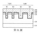
依據一些實施例,遮罩層150和220用作後續製程中形成導線的蝕刻遮罩。雖然溝槽151、152、153和154的寬度W1、W2、W3和W4彼此大致相等,形成於溝槽151和152的內壁N1和N2上方的遮罩層220具有比溝槽151、152、153和154更窄的溝槽222和224。因此,遮罩層220的形成可透過使用遮罩層220作為蝕刻遮罩而使後續形成的導線變窄。According to some embodiments, the mask layers 150 and 220 are used as etching masks for forming wires in subsequent processes. Although the widths W1, W2, W3, and W4 of the
依據一些實施例,如第1K圖所示,移除在溝槽222、224、153和154下方的硬遮罩層140、遮罩層130和介電層 120的部分,以形成在硬遮罩層140、遮罩層130和介電層120中的溝槽R1、R2、R3和R4。According to some embodiments, as shown in FIG. 1K, portions of
依據一些實施例,溝槽R1、R2、R3和R4通過硬遮罩層140和遮罩層130並穿透進入介電層120。依據一些實施例,溝槽R1、R2、R3和R4分別具有寬度W7、W8、W9和W10。依據一些實施例,寬度W7或W8小於寬度W9或W10。According to some embodiments, trenches R1 , R2 , R3 , and R4 pass through
依據一些實施例,移除製程包含使用遮罩層150和220作為蝕刻遮罩的蝕刻製程。遮罩層150和220可在移除製程期間被消耗。在一些實施例中,硬遮罩層140的上部在移除製程期間被消耗。According to some embodiments, the removal process includes an etch process using
由於在移除製程期間遮罩層220覆蓋區域110A中的硬遮罩層140,因此留在區域110A中的硬遮罩層140比留在區域110B中的硬遮罩層140更厚。也就是說,區域110A中的硬遮罩層140的厚度T9比區域110B中的硬遮罩層140的厚度T10更大。在一些實施例中,留在區域110A中的硬遮罩層140也被稱為厚的部分,而留在區域110B中的硬遮罩層140也被稱為薄的部分。在一些實施例中,厚的部分與薄的部分之間的邊界與遮罩層220的側壁229(如第1J圖所示)大致對齊。Since the
依據一些實施例,如第1L圖所示,阻障層240沉積於硬遮罩層140、遮罩層130和介電層120上方。阻障層240可在熱製程或熱循環期間防止後續沉積的導電材料(其將在後面更詳細地描述)的金屬離子擴散進入介電層120。阻障層240也可被稱為擴散阻障層。According to some embodiments,
在一些實施例中,阻障層240由耐火金屬材料(例如 鉭(Ta)、鈦(Ti)、氮化鉭、氮化鈦、一個或多個其他合適的材料或前述之組合)製成,或包含前述材料。在一些實施例中,阻障層240透過使用物理氣相沉積製程、原子層沉積製程、一個或多個其他可應用的製程或前述之組合沉積。在一些實施例中,順應性地沉積阻障層240。In some embodiments, the
依據一些實施例,如第1L圖所示,導電材料層250形成於阻障層240上方。依據一些實施例,溝槽R1、R2、R3和R4填充導電材料層250和阻障層240。在一些實施例中,導電材料層250由金屬材料(例如銅、鋁、鎢、鈦、鎳、金、鉑、銀、一個或多個其他合適的材料或前述之組合)製成,或包含前述材料。According to some embodiments, as shown in FIG. 1L , a
導電材料層250可為單一層或具有多個堆疊層。導電材料層250透過使用電鍍製程、物理氣相沉積製程、化學氣相沉積製程、無電電鍍製程、其他可應用的製程或前述之組合沉積。The
依據一些實施例,如第1M圖所示,移除在溝槽R1、R2、R3和R4、硬遮罩層140和遮罩層130之外的導電材料層250和阻障層240。依據一些實施例,留在溝槽R1、R2、R3和R4中的導電材料層250和阻障層240分別在溝槽R1、R2、R3和R4中形成導電結構L1、L2、L3和L4。According to some embodiments, as shown in FIG. 1M , the
依據一些實施例,導電結構L1、L2、L3和L4包含導線。依據一些實施例,導電結構L1、L2、L3和L4分別具有寬度(或線寬)W11、W12、W13和W14。由於寬度W7或W8小於寬度W9或W10(如第1K圖所示),因此寬度W11或W12小於寬度 W13或W14。依據一些實施例,寬度W11和W12彼此大致相等。依據一些實施例,寬度W13和W14彼此大致相等。According to some embodiments, the conductive structures L1, L2, L3 and L4 comprise wires. According to some embodiments, the conductive structures L1 , L2 , L3 and L4 have widths (or line widths) W11 , W12 , W13 and W14 , respectively. Since width W7 or W8 is smaller than width W9 or W10 (as shown in Fig. 1K), width W11 or W12 is smaller than width W13 or W14. According to some embodiments, widths W11 and W12 are approximately equal to each other. According to some embodiments, widths W13 and W14 are approximately equal to each other.
依據一些實施例,導電結構L1和L2位於區域110A中,而導電結構L3和L4位於區域110B中。依據一些實施例,導電結構L1與導電結構L2之間的距離D1小於導電結構L3與導電結構L4之間的距離D2。According to some embodiments, the conductive structures L1 and L2 are located in the
區域110A和110B可分別被稱為小間距區和大間距區。一個區域的間距(pitch)等於導電結構的其中一者的寬度與此區域中兩相鄰導電結構之間的間隔的總和。依據一些實施例,區域110A的間距等於寬度W11(或W12)與距離D1的總和。依據一些實施例,區域110B的間距等於寬度W13(或W14)與距離D2的總和。由於寬度W11(或W12)小於寬度W13(或W14)且距離D1小於距離D2,區域110A的間距小於區域110B的間距。
依據一些實施例,移除製程包含平坦化製程。因此,依據一些實施例,導電結構L1、L2、L3和L4的頂表面S1、S2、S3、S4和介電層120的頂表面122共平面。According to some embodiments, the removal process includes a planarization process. Therefore, according to some embodiments, the top surfaces S1 , S2 , S3 , S4 of the conductive structures L1 , L2 , L3 , and L4 are coplanar with the
第2A-2C圖為依據一些實施例之形成半導體裝置結構的製程的各種階段的剖面示意圖。依據一些實施例,第2A-2C圖的實施例相似於第1A-1M圖的實施例,除了第2A-2C圖的實施例先移除區域110B中的遮罩層220(如第2B圖所示),接著移除覆蓋底表面B1和B2的遮罩層220(如第2C圖所示)。2A-2C are schematic cross-sectional views of various stages in the process of forming a semiconductor device structure in accordance with some embodiments. According to some embodiments, the embodiment of FIGS. 2A-2C is similar to the embodiment of FIGS. 1A-1M , except that the embodiment of FIGS. 2A-2C first removes masking
在第1F圖的步驟之後,依據一些實施例,如第2A圖所示,光阻層230形成於區域110A中的遮罩層220上方。之後,依據一些實施例,如第2B圖所示,移除區域110B中的遮罩 層220。依據一些實施例,移除製程包含使用光阻層230作為蝕刻遮罩的蝕刻製程。After the steps of FIG. 1F , according to some embodiments, a
依據一些實施例,如第2C圖所示,移除光阻層230。依據一些實施例,如第2C圖所示,移除覆蓋底表面B1和B2的遮罩層220,以形成遮罩層220中的溝槽222和224。依據一些實施例,溝槽222和224分別暴露出底表面B1和B2。之後,依據一些實施例,進行第1K-1M圖的步驟以形成導電結構L1、L2、L3和L4(如第1M圖所示)。According to some embodiments, as shown in FIG. 2C, the
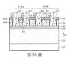
第3A-3H圖為依據一些實施例之形成半導體裝置結構的製程的各種階段的剖面示意圖。在第1E圖的步驟之後,依據一些實施例,如第3A圖所示,遮罩層310形成於遮罩層150的頂表面155以及溝槽151、152、153和154的內壁N1、N2、N3和N4上方。3A-3H are schematic cross-sectional views of various stages in the process of forming a semiconductor device structure in accordance with some embodiments. After the step in FIG. 1E, according to some embodiments, as shown in FIG. 3A, a
在一些實施例中,在內壁N1、N2、N3和N4上方的遮罩層310的厚度T4沿著遠離介電層120的方向V1增加。依據一些實施例,遮罩層310分別在溝槽151、152、153和154中具有溝槽312、314、316和318。依據一些實施例,溝槽312、314、316和318分別暴露出溝槽151、152、153和154的底表面B1、B2、B3和B4。In some embodiments, the thickness T4 of the
依據一些實施例,覆蓋頂表面155的遮罩層310比覆蓋溝槽151、152、153和154的內壁N1、N2、N3和N4的遮罩層310更厚。也就是說,依據一些實施例,覆蓋頂表面155的遮罩層310的最大厚度T5大於在內壁N1、N2、N3和N4上方的遮罩層310的最大厚度T4’。According to some embodiments, the
依據一些實施例,遮罩層310也被稱為抗轟擊(anti-bombardment layer)層。依據一些實施例,遮罩層310用於在後續用來形成在介電層120中的溝槽的蝕刻製程(例如乾蝕刻製程)期間維持其下方的遮罩層150的高度較長時間。According to some embodiments, the
依據一些實施例,遮罩層310由抗轟擊材料(例如氮化鈦或氮化鉭)製成。依據一些實施例,遮罩層310透過使用化學氣相沉積製程或原子層沉積製程形成。依據一些實施例,遮罩層310在第一沉積壓力下沉積。依據一些實施例,遮罩層310以第一沉積功率沉積。According to some embodiments, the
依據一些實施例,如第3B圖所示,遮罩層220形成於遮罩層310和透過溝槽151、152、153和154暴露的硬遮罩層140上方。依據一些實施例,遮罩層220覆蓋溝槽151、152、153和154的內壁N1、N2、N3和N4以及底表面B1、B2、B3和B4。According to some embodiments,
依據一些實施例,遮罩層220也被稱為抗化學蝕刻保護層。依據一些實施例,遮罩層220用以在後續用來形成在介電層120中的溝槽的蝕刻製程(例如乾蝕刻製程)期間保護內壁N1、N2、N3和N4。依據一些實施例,遮罩層220直接接觸遮罩層150和310以及硬遮罩層140。According to some embodiments, the
在一些實施例中,在頂表面155上方的遮罩層220的第一厚度T6大於在內壁N1、N2、N3和N4上方的遮罩層220的第二厚度T7。依據一些實施例,第二厚度T7大於在底表面B1、B2、B3和B4上方的遮罩層220的第三厚度T8。In some embodiments, the first thickness T6 of the
依據一些實施例,遮罩層220和310由不同材料製成。依據一些實施例,遮罩層220由抗化學蝕刻材料(例如氮化 物材料(例如SiON、SiCN、SiN)或低溫氧化物材料(例如二氧化矽))製成,或包含前述材料。遮罩層220透過使用化學氣相沉積製程、原子層沉積製程、一個或多個其他可應用的製程或前述之組合沉積。According to some embodiments, mask layers 220 and 310 are made of different materials. According to some embodiments, the
依據一些實施例,遮罩層220在第二沉積壓力下沉積。依據一些實施例,遮罩層220以第二沉積功率沉積。假如沉積壓力高且沉積功率低,沉積層傾向沉積於溝槽之外。假如沉積壓力低且沉積功率大,沉積層傾向沉積於溝槽中。因此,依據一些實施例,第一沉積壓力大於第二沉積壓力。依據一些實施例,第一沉積功率小於第二沉積功率。According to some embodiments,
依據一些實施例,如第3C圖所示,移除底表面B1、B2、B3和B4上方的遮罩層220。依據一些實施例,移除製程形成遮罩層220中的溝槽222、224、226和228。依據一些實施例,溝槽222、224、226和228分別位於溝槽312、314、316和318中。依據一些實施例,溝槽222、224、226和228分別暴露出底表面B1、B2、B3和B4。依據一些實施例,移除製程包含蝕刻製程(例如乾蝕刻製程或濕蝕刻製程)。According to some embodiments, as shown in FIG. 3C , the
依據一些實施例,如第3D圖所示,光阻層230形成於區域110A中的遮罩層220上方。依據一些實施例,光阻層230填充溝槽151和152。依據一些實施例,如第3E圖所示,移除區域110B中的遮罩層220和310。依據一些實施例,移除製程包含蝕刻製程(例如乾蝕刻製程)。According to some embodiments, as shown in FIG. 3D , the
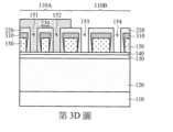
依據一些實施例,如第3F圖所示,移除光阻層230。在一些實施例中,溝槽222與溝槽224之間的距離D1小於 溝槽153與溝槽154之間的距離D2。依據一些實施例,遮罩層150、220和310用作在後續用來形成導線的製程中的蝕刻遮罩。According to some embodiments, as shown in FIG. 3F, the
依據一些實施例,如第3G圖所示,移除在溝槽222、224、153和154下方的硬遮罩層140、遮罩層130和介電層120的部分,以形成在硬遮罩層140、遮罩層130和介電層120中的溝槽R1、R2、R3和R4。According to some embodiments, as shown in FIG. 3G , portions of
依據一些實施例,溝槽R1、R2、R3和R4通過硬遮罩層140和遮罩層130並穿透進入介電層120。依據一些實施例,溝槽R1、R2、R3和R4分別具有寬度W7、W8、W9和W10。依據一些實施例,寬度W7或W8小於寬度W9或W10。According to some embodiments, trenches R1 , R2 , R3 , and R4 pass through
依據一些實施例,移除製程包含使用遮罩層150、220和310作為蝕刻遮罩的蝕刻製程。遮罩層150、220和310可在移除製程期間被消耗。在一些實施例中,硬遮罩層140的上部在移除製程期間被消耗。According to some embodiments, the removal process includes an etching process using
依據一些實施例,如第3F和3G圖所示,由於遮罩層(或抗轟擊層)310覆蓋遮罩層150的頂表面155,因此遮罩層150的高度在移除製程期間維持較長時間。依據一些實施例,如第3F和3G圖所示,由於遮罩層220由抗化學蝕刻材料製成,因此遮罩層220的溝槽222和224的寬度W5和W6在移除製程期間維持較長時間。因此,如第3F和3G圖所示,遮罩層220和310的形成可改善溝槽R1和R2的良率。According to some embodiments, as shown in Figures 3F and 3G, since the mask layer (or anti-bombardment layer) 310 covers the
依據一些實施例,如第3G圖所示,阻障層240沉積於硬遮罩層140、遮罩層130和介電層120上方。阻障層240可在熱製程或熱循環期間防止後續沉積的導電材料(其將在後面更 詳細地描述)的金屬離子擴散進入介電層120。阻障層240也可被稱為擴散阻障層。According to some embodiments,
在一些實施例中,阻障層240由耐火金屬材料(例如鉭(Ta)、鈦(Ti)、氮化鉭、氮化鈦、一個或多個其他合適的材料或前述之組合)製成,或包含前述材料。在一些實施例中,阻障層240透過使用物理氣相沉積製程、原子層沉積製程、一個或多個其他可應用的製程或前述之組合沉積。在一些實施例中,順應性地沉積阻障層240。In some embodiments, the
依據一些實施例,如第3G圖所示,導電材料層250形成於阻障層240上方。依據一些實施例,溝槽R1、R2、R3和R4填充導電材料層250和阻障層240。According to some embodiments, as shown in FIG. 3G , a
依據一些實施例,如第3H圖所示,移除在溝槽R1、R2、R3和R4、硬遮罩層140和遮罩層130之外的導電材料層250和阻障層240。依據一些實施例,留在溝槽R1、R2、R3和R4中的導電材料層250和阻障層240分別在溝槽R1、R2、R3和R4中形成導電結構L1、L2、L3和L4。According to some embodiments, as shown in FIG. 3H , the
依據一些實施例,導電結構L1、L2、L3和L4包含導線。依據一些實施例,導電結構L1、L2、L3和L4分別具有寬度(或線寬)W11、W12、W13和W14。由於寬度W7或W8小於寬度W9或W10(如第3G圖所示),因此寬度W11或W12小於寬度W13或W14。According to some embodiments, the conductive structures L1, L2, L3 and L4 comprise wires. According to some embodiments, the conductive structures L1 , L2 , L3 and L4 have widths (or line widths) W11 , W12 , W13 and W14 , respectively. Since width W7 or W8 is smaller than width W9 or W10 (as shown in FIG. 3G), width W11 or W12 is smaller than width W13 or W14.
依據一些實施例,導電結構L1和L2位於區域110A中,而導電結構L3和L4位於區域110B中。依據一些實施例,導電結構L1與導電結構L2之間的距離D1小於導電結構L3與導 電結構L4之間的距離D2。According to some embodiments, the conductive structures L1 and L2 are located in the
依據一些實施例,移除製程包含平坦化製程。因此,依據一些實施例,導電結構L1、L2、L3和L4的頂表面S1、S2、S3、S4和介電層120的頂表面122共平面。According to some embodiments, the removal process includes a planarization process. Therefore, according to some embodiments, the top surfaces S1 , S2 , S3 , S4 of the conductive structures L1 , L2 , L3 , and L4 are coplanar with the
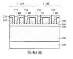
第4A-4F圖為依據一些實施例之形成半導體裝置結構的製程的各種階段的剖面示意圖。在第1E圖的步驟之後,依據一些實施例,如第4A圖所示,遮罩層220順應性地形成於遮罩層150的頂表面155、溝槽151、152、153和154的內壁N1、N2、N3和N4以及底表面B1、B2、B3和B4上方。依據一些實施例,遮罩層220由抗化學蝕刻材料(例如氮化物材料(例如SiON、SiCN或SiN)或低溫氧化物材料(例如二氧化矽))製成,或包含前述材料。4A-4F are schematic cross-sectional views of various stages in the process of forming a semiconductor device structure in accordance with some embodiments. After the step in FIG. 1E , according to some embodiments, as shown in FIG. 4A , masking
依據一些實施例,如第4B圖所示,移除在底表面B1、B2、B3和B4上方的遮罩層220。依據一些實施例,遮罩層220具有溝槽222、224、226和228。依據一些實施例,如第4C圖所示,遮罩層310形成於遮罩層220上方。According to some embodiments, as shown in FIG. 4B , the
依據一些實施例,遮罩層310覆蓋遮罩層220的頂表面221和溝槽222、224、226和228的內壁222a、224a、226a和228a。在一些實施例中,在內壁222a、224a、226a和228a上方的遮罩層310的厚度T4沿著遠離介電層120的方向V1增加。依據一些實施例,遮罩層310由抗轟擊材料(例如氮化物材料(例如氮化鈦或氮化鉭))製成。依據一些實施例,遮罩層220和310由不同材料製成。According to some embodiments, the
依據一些實施例,如第4D圖所示,移除在區域110B 中的遮罩層220和310。依據一些實施例,如第4E圖所示,移除移除在溝槽222、224、153和154下方的硬遮罩層140、遮罩層130和介電層120的部分,以形成在硬遮罩層140、遮罩層130和介電層120中的溝槽R1、R2、R3和R4。According to some embodiments, mask layers 220 and 310 are removed in
依據一些實施例,溝槽R1、R2、R3和R4通過硬遮罩層140和遮罩層130並穿透進入介電層120。依據一些實施例,移除製程包含使用遮罩層150、220和310作為蝕刻遮罩的蝕刻製程。遮罩層150、220和310可在移除製程期間被消耗。在一些實施例中,硬遮罩層140的上部在移除製程期間被消耗。According to some embodiments, trenches R1 , R2 , R3 , and R4 pass through
依據一些實施例,如第4D和4E圖所示,由於遮罩層(或抗轟擊層)310覆蓋遮罩層150的頂表面155,因此遮罩層150的高度在移除製程期間維持較長時間。依據一些實施例,如第4D和4E圖所示,由於遮罩層220由抗化學蝕刻材料製成,因此遮罩層220的溝槽222和224的寬度W5和W6在移除製程期間維持較長時間。因此,如第4D和4E圖所示,遮罩層220和310的形成可改善溝槽R1和R2的良率。According to some embodiments, as shown in Figures 4D and 4E, since the mask layer (or anti-bombardment layer) 310 covers the
依據一些實施例,如第4E圖所示,阻障層240沉積於硬遮罩層140、遮罩層130和介電層120上方。依據一些實施例,如第4E圖所示,導電材料層250形成於阻障層240上方。According to some embodiments,
依據一些實施例,如第4F圖所示,移除在溝槽R1、R2、R3和R4、硬遮罩層140和遮罩層130之外的導電材料層250和阻障層240。依據一些實施例,留在溝槽R1、R2、R3和R4中的導電材料層250和阻障層240分別在溝槽R1、R2、R3和R4中形成導電結構L1、L2、L3和L4。According to some embodiments, as shown in FIG. 4F , the
依據一些實施例,導電結構L1、L2、L3和L4包含導線。依據一些實施例,導電結構L1、L2、L3和L4分別具有寬度(或線寬)W11、W12、W13和W14。依據一些實施例,寬度W11或W12小於寬度W13或W14。依據一些實施例,導電結構L1與導電結構L2之間的距離D1小於導電結構L3與導電結構L4之間的距離D2。According to some embodiments, the conductive structures L1, L2, L3 and L4 comprise wires. According to some embodiments, the conductive structures L1 , L2 , L3 and L4 have widths (or line widths) W11 , W12 , W13 and W14 , respectively. According to some embodiments, the width W11 or W12 is smaller than the width W13 or W14. According to some embodiments, the distance D1 between the conductive structure L1 and the conductive structure L2 is smaller than the distance D2 between the conductive structure L3 and the conductive structure L4.
依據一些實施例,移除製程包含平坦化製程。因此,依據一些實施例,導電結構L1、L2、L3和L4的頂表面S1、S2、S3、S4和介電層120的頂表面122共平面。According to some embodiments, the removal process includes a planarization process. Therefore, according to some embodiments, the top surfaces S1 , S2 , S3 , S4 of the conductive structures L1 , L2 , L3 , and L4 are coplanar with the
依據一些實施例,提供半導體裝置結構的形成方法。這些(用於形成半導體裝置結構的)方法包含:在介電層上方形成第一遮罩層;在第一遮罩層的第一溝槽的內壁上方順應性地形成第二遮罩層;以及通過第一溝槽移除介電層,以在介電層中形成第二溝槽。在內壁上方形成第二遮罩層能使第二溝槽變窄。According to some embodiments, methods of forming semiconductor device structures are provided. These methods (for forming semiconductor device structures) include: forming a first mask layer over the dielectric layer; conformally forming a second mask layer over inner walls of the first trench of the first mask layer; and removing the dielectric layer through the first trench to form a second trench in the dielectric layer. Forming the second mask layer over the inner wall can narrow the second trench.
依據一些實施例,提供半導體裝置結構的形成方法,此方法包含在介電層上方形成第一遮罩層。第一遮罩層具有第一溝槽,第一溝槽具有內壁和底表面。此方法包含在第一溝槽中形成第二遮罩層。此方法包含移除覆蓋底表面的第二遮罩層,以在第二遮罩層中形成第二溝槽。第二溝槽暴露出底表面且在介電層的第一部分上方。留下的第二遮罩層覆蓋內壁。此方法包含移除第一部分、第一遮罩層和第二遮罩層,以在介電層中形成第三溝槽。此方法包含在第三溝槽中形成導電結構。According to some embodiments, a method of forming a semiconductor device structure is provided, the method including forming a first mask layer over a dielectric layer. The first mask layer has a first groove, and the first groove has an inner wall and a bottom surface. The method includes forming a second mask layer in the first trench. The method includes removing a second mask layer covering the bottom surface to form a second trench in the second mask layer. The second trench exposes the bottom surface and is above the first portion of the dielectric layer. A second masking layer is left covering the inner wall. The method includes removing the first portion, the first mask layer and the second mask layer to form a third trench in the dielectric layer. The method includes forming a conductive structure in the third trench.
在一些其他實施例中,其中在第一溝槽中形成第二遮罩層的步驟包括在內壁和底表面上方順應性地沉積第二遮罩層。In some other embodiments, the step of forming the second mask layer in the first trench includes conformally depositing the second mask layer over the inner wall and bottom surface.
在一些其他實施例中,其中第二遮罩層更順應性地沉積於第一遮罩層的頂表面上方。In some other embodiments, the second mask layer is more conformally deposited over the top surface of the first mask layer.
在一些其他實施例中,其中在頂表面上方的第二遮罩層的第一厚度大於在內壁上方的第二遮罩層的第二厚度,且第二厚度大於在底表面上方的第二遮罩層的第三厚度。In some other embodiments, wherein the first thickness of the second mask layer above the top surface is greater than the second thickness of the second mask layer above the inner wall, and the second thickness is greater than the second thickness of the second mask layer above the bottom surface. The third thickness of the mask layer.
在一些其他實施例中,其中在形成導電結構之後,導電結構的第一頂表面與介電層的第二頂表面共平面。In some other embodiments, wherein after the conductive structure is formed, the first top surface of the conductive structure is coplanar with the second top surface of the dielectric layer.
在一些其他實施例中,其中第一遮罩層和第二遮罩層由相同材料製成。In some other embodiments, the first mask layer and the second mask layer are made of the same material.
在一些其他實施例中,其中介電層和第一遮罩層由不同材料製成。In some other embodiments, the dielectric layer and the first mask layer are made of different materials.
依據一些實施例,提供半導體裝置結構的形成方法,此方法包含在介電層上方形成第一遮罩層。第一遮罩層具有第一溝槽和第二溝槽,且第一溝槽具有第一內壁和第一底表面。此方法包含在第一內壁上方順應性形成第二遮罩層。第二遮罩層具有在第一溝槽中的第三溝槽並暴露出第一底表面,第三溝槽比第二溝槽窄,且第三溝槽和第二溝槽分別在介電層的第一部分和第二部分上方。此方法包含移除第一部分、第二部分、第一遮罩層和第二遮罩層,以在介電層中形成第四溝槽和第五溝槽。第四溝槽比第五溝槽窄。此方法包含分別在第四溝槽和第五溝槽中形成第一導電結構和第二導電結構。According to some embodiments, a method of forming a semiconductor device structure is provided, the method including forming a first mask layer over a dielectric layer. The first mask layer has a first groove and a second groove, and the first groove has a first inner wall and a first bottom surface. The method includes conformally forming a second mask layer over the first inner wall. The second mask layer has a third groove in the first groove and exposes the first bottom surface, the third groove is narrower than the second groove, and the third groove and the second groove are respectively separated in the dielectric layer above the first part and the second part. The method includes removing the first portion, the second portion, the first mask layer, and the second mask layer to form fourth and fifth trenches in the dielectric layer. The fourth groove is narrower than the fifth groove. The method includes forming a first conductive structure and a second conductive structure in the fourth trench and the fifth trench, respectively.
在一些其他實施例中,上述方法更包含在形成第一遮罩層之前,在介電層上方形成第三遮罩層,其中第一遮罩層形成於第三遮罩層上,第二溝槽和第三溝槽分別暴露出第三遮罩層的第三部分和第四部分;以及移除第一部分、第二部分、第一遮罩層和第二遮罩層的步驟更包含移除第三部分和第四部份。In some other embodiments, the above method further includes forming a third mask layer on the dielectric layer before forming the first mask layer, wherein the first mask layer is formed on the third mask layer, and the second trench The groove and the third groove respectively expose the third part and the fourth part of the third mask layer; and the step of removing the first part, the second part, the first mask layer and the second mask layer further includes removing Part Three and Part Four.
在一些其他實施例中,其中形成第一導電結構和第二導電結構的步驟包含在移除第一部分、第二部分、第三部分、第四部份、第一遮罩層和第二遮罩層之後,在第三遮罩層和介電層上方形成導電材料層,其中第四溝槽和第五溝槽填充導電材料層;以及移除在第四溝槽和第五溝槽以及第三遮罩層之外的導電材料層。In some other embodiments, the step of forming the first conductive structure and the second conductive structure includes removing the first part, the second part, the third part, the fourth part, the first mask layer and the second mask layer, a conductive material layer is formed over the third mask layer and the dielectric layer, wherein the fourth trench and the fifth trench are filled with the conductive material layer; and the fourth trench and the fifth trench and the third trench are removed A layer of conductive material other than the mask layer.
在一些其他實施例中,其中移除在第四溝槽和第五溝槽以及第三遮罩層之外的導電材料層的步驟包含進行平坦化製程。In some other embodiments, the step of removing the conductive material layer outside the fourth and fifth trenches and the third mask layer includes performing a planarization process.
在一些其他實施例中,其中第三遮罩層和第一遮罩層由不同材料製成。In some other embodiments, the third mask layer and the first mask layer are made of different materials.
在一些其他實施例中,其中第三遮罩層具有第五部分和第六部分,第五部分被第二遮罩層覆蓋,第六部分被第一遮罩層覆蓋且不被第二遮罩層覆蓋,且在移除第一部分、第二部分、第一遮罩層和第二遮罩層之後,第六部分比第五部分薄。In some other embodiments, wherein the third mask layer has a fifth part and a sixth part, the fifth part is covered by the second mask layer, and the sixth part is covered by the first mask layer and not covered by the second mask layer covering, and after removing the first part, the second part, the first mask layer and the second mask layer, the sixth part is thinner than the fifth part.
在一些其他實施例中,其中第一溝槽的第一寬度與第二溝槽的第二寬度大致相等。In some other embodiments, the first width of the first trench is substantially equal to the second width of the second trench.
依據一些實施例,提供半導體裝置結構的形成方法,此方法包含在介電層上方形成第一遮罩層。第一遮罩層具有第一溝槽和第二溝槽,且第一溝槽具有第一內壁和第一底表面。此方法包含在第一遮罩層的頂表面和第一內壁上方形成第二遮罩層。在第一內壁上方的第二遮罩層的厚度沿遠離介電層的方向增加,第二遮罩層具有在第一溝槽中的第三溝槽並暴露出第一底表面,且第三溝槽和第二溝槽分別在介電層的第一部分和第二部分上方。此方法包含移除第一部分、第二部分、第一遮罩層和第二遮罩層,以在介電層中形成第四溝槽和第五溝槽,第四溝槽比第五溝槽窄。此方法包含分別在第四溝槽和第五溝槽中形成第一導電結構和第二導電結構。According to some embodiments, a method of forming a semiconductor device structure is provided, the method including forming a first mask layer over a dielectric layer. The first mask layer has a first groove and a second groove, and the first groove has a first inner wall and a first bottom surface. The method includes forming a second mask layer over a top surface of the first mask layer and the first inner wall. The thickness of the second mask layer above the first inner wall increases in a direction away from the dielectric layer, the second mask layer has a third groove in the first groove and exposes the first bottom surface, and the second mask layer The third trench and the second trench are over the first and second portions of the dielectric layer, respectively. The method includes removing the first portion, the second portion, the first mask layer, and the second mask layer to form fourth trenches and fifth trenches in the dielectric layer, the fourth trenches being larger than the fifth trenches narrow. The method includes forming a first conductive structure and a second conductive structure in the fourth trench and the fifth trench, respectively.
在一些其他實施例中,其中覆蓋頂表面的第二遮罩層比覆蓋第一內壁的第二遮罩層更厚。In some other embodiments, the second mask layer covering the top surface is thicker than the second mask layer covering the first inner wall.
在一些其他實施例中,上述方法更包含在第一遮罩層的頂表面和第一內壁上方形成第二遮罩層之後以及在移除第一部分、第二部分、第一遮罩層和第二遮罩層之前,在第二遮罩層上方形成第三遮罩層並覆蓋第一內壁,以及移除第一部分、第二部分、第一遮罩層和第二遮罩層的步驟更包含移除第三遮罩層。In some other embodiments, the above method further includes after forming the second mask layer over the top surface and the first inner wall of the first mask layer and after removing the first portion, the second portion, the first mask layer, and Before the second mask layer, forming a third mask layer over the second mask layer and covering the first inner wall, and removing the first part, the second part, the first mask layer and the second mask layer It further includes removing the third mask layer.
在一些其他實施例中,其中第二遮罩層和第三遮罩層由不同材料製成。In some other embodiments, the second mask layer and the third mask layer are made of different materials.
在一些其他實施例中,上述方法更包含在第一遮罩層的頂表面和第一內壁上方形成第二遮罩層之前,在頂表面和第一內壁上方形成第三遮罩層,第二遮罩層形成於第三遮罩 層上方,以及移除第一部分、第二部分、第一遮罩層和第二遮罩層的步驟更包含移除第三遮罩層。In some other embodiments, the above method further includes forming a third mask layer over the top surface and the first inner wall before forming the second mask layer over the top surface and the first inner wall of the first mask layer, The second mask layer is formed on the third mask layer, and the step of removing the first portion, the second portion, the first mask layer and the second mask layer further includes removing the third mask layer.
在一些其他實施例中,其中第二遮罩層和第三遮罩層由不同材料製成。In some other embodiments, the second mask layer and the third mask layer are made of different materials.
前述內文概述了許多實施例的特徵,使本技術領域中具有通常知識者可以從各個方面更佳地了解本發明實施例。本技術領域中具有通常知識者應可理解,且可輕易地以本發明實施例為基礎來設計或修飾其他製程及結構,並以此達到相同的目的及/或達到與在此介紹的實施例等相同之優點。本技術領域中具有通常知識者也應了解這些相等的結構並未背離本發明的發明精神與範圍。在不背離本發明的發明精神與範圍之前提下,可對本發明進行各種改變、置換或修改。The foregoing text summarizes the features of many embodiments, so that those skilled in the art can better understand the embodiments of the present invention from various aspects. Those skilled in the art should understand and can easily design or modify other processes and structures based on the embodiments of the present invention, so as to achieve the same purpose and/or achieve the same as the embodiments introduced here and so on. Those skilled in the art should also realize that such equivalent structures do not depart from the spirit and scope of the invention. Various changes, substitutions or modifications can be made in the present invention without departing from the spirit and scope of the present invention.
110‧‧‧半導體基底110‧‧‧Semiconductor substrate
110A、110B‧‧‧區域110A, 110B‧‧‧area
120‧‧‧介電層120‧‧‧dielectric layer
122、S1、S2、S3、S4‧‧‧頂表面122, S1, S2, S3, S4‧‧‧top surface
R1、R2、R3、R4‧‧‧溝槽R1, R2, R3, R4‧‧‧groove
240‧‧‧阻障層240‧‧‧barrier layer
250‧‧‧導電材料層250‧‧‧conductive material layer
D1、D2‧‧‧距離D1, D2‧‧‧distance
L1、L2、L3、L4‧‧‧導電結構L1, L2, L3, L4‧‧‧conductive structure
W11、W12、W13、W14‧‧‧寬度W11, W12, W13, W14‧‧‧width
Claims (10)
Translated fromChineseApplications Claiming Priority (4)
| Application Number | Priority Date | Filing Date | Title |
|---|---|---|---|
| US201762583121P | 2017-11-08 | 2017-11-08 | |
| US62/583,121 | 2017-11-08 | ||
| US15/884,760 | 2018-01-31 | ||
| US15/884,760US10510671B2 (en) | 2017-11-08 | 2018-01-31 | Method for forming semiconductor device structure with conductive line |
Publications (2)
| Publication Number | Publication Date |
|---|---|
| TW201919100A TW201919100A (en) | 2019-05-16 |
| TWI803495Btrue TWI803495B (en) | 2023-06-01 |
Family
ID=66328896
Family Applications (1)
| Application Number | Title | Priority Date | Filing Date |
|---|---|---|---|
| TW107117734ATWI803495B (en) | 2017-11-08 | 2018-05-24 | Methods for forming semiconductor device structures |
Country Status (3)
| Country | Link |
|---|---|
| US (3) | US10510671B2 (en) |
| CN (1) | CN109755176B (en) |
| TW (1) | TWI803495B (en) |
Families Citing this family (2)
| Publication number | Priority date | Publication date | Assignee | Title |
|---|---|---|---|---|
| US10699943B2 (en)* | 2018-04-30 | 2020-06-30 | Taiwan Semiconductor Manufacturing Company, Ltd. | Method of forming contacts in a semiconductor device |
| US12219709B2 (en)* | 2022-07-29 | 2025-02-04 | Taiwan Semiconductor Manufacturing Company, Ltd. | Forming trench in IC chip through multiple trench formation and deposition processes |
Citations (10)
| Publication number | Priority date | Publication date | Assignee | Title |
|---|---|---|---|---|
| US20030044725A1 (en)* | 2001-07-24 | 2003-03-06 | Chen-Chiu Hsue | Dual damascene process using metal hard mask |
| US20040219707A1 (en)* | 2003-04-29 | 2004-11-04 | Won-Ho Lee | Method for fabricating complementary metal oxide semiconductor image sensor having redundancy module |
| US20090001341A1 (en)* | 2007-06-29 | 2009-01-01 | Matthew Breitwisch | Phase Change Memory with Tapered Heater |
| TW201532143A (en)* | 2014-01-24 | 2015-08-16 | Applied Materials Inc | Methods for etching a dielectric barrier layer in a dual damascene structure |
| TW201537678A (en)* | 2014-03-21 | 2015-10-01 | Taiwan Semiconductor Mfg | Interconnect structure and manufacturing method thereof |
| TW201635379A (en)* | 2014-12-26 | 2016-10-01 | 台灣積體電路製造股份有限公司 | Fin field effect transistor structure and manufacturing method thereof |
| TW201709465A (en)* | 2015-08-27 | 2017-03-01 | Globalfoundries Us Inc | Integrated circuit structure with metal crack stop and forming method thereof |
| TW201732975A (en)* | 2016-03-02 | 2017-09-16 | 台灣積體電路製造股份有限公司 | Wire structure and manufacturing method |
| TW201735244A (en)* | 2016-03-24 | 2017-10-01 | 台灣積體電路製造股份有限公司 | Deep trench isolation structure and method of forming same |
| TW201738931A (en)* | 2016-04-28 | 2017-11-01 | 台灣積體電路製造股份有限公司 | Method of forming a semiconductor device |
Family Cites Families (6)
| Publication number | Priority date | Publication date | Assignee | Title |
|---|---|---|---|---|
| JP4377040B2 (en)* | 2000-07-24 | 2009-12-02 | Necエレクトロニクス株式会社 | Semiconductor manufacturing method |
| KR100393968B1 (en)* | 2000-12-29 | 2003-08-06 | 주식회사 하이닉스반도체 | method for forming dual damascene of semiconductor device |
| KR20080006713A (en)* | 2006-07-13 | 2008-01-17 | 삼성전자주식회사 | Apparatus and method for allocating data block size to portable media in portable terminal |
| KR20080067131A (en)* | 2007-01-15 | 2008-07-18 | 삼성전자주식회사 | Pattern formation method of semiconductor device |
| CN101308809A (en)* | 2007-05-17 | 2008-11-19 | 力晶半导体股份有限公司 | Method for manufacturing aluminum conductor |
| US9698100B2 (en)* | 2015-08-19 | 2017-07-04 | Taiwan Semiconductor Manufacturing Company, Ltd. | Structure and method for interconnection |
- 2018
- 2018-01-31USUS15/884,760patent/US10510671B2/enactiveActive
- 2018-03-29CNCN201810272577.6Apatent/CN109755176B/enactiveActive
- 2018-05-24TWTW107117734Apatent/TWI803495B/enactive
- 2019
- 2019-12-16USUS16/715,215patent/US10770401B2/enactiveActive
- 2020
- 2020-09-02USUS17/010,530patent/US10879186B1/enactiveActive
Patent Citations (10)
| Publication number | Priority date | Publication date | Assignee | Title |
|---|---|---|---|---|
| US20030044725A1 (en)* | 2001-07-24 | 2003-03-06 | Chen-Chiu Hsue | Dual damascene process using metal hard mask |
| US20040219707A1 (en)* | 2003-04-29 | 2004-11-04 | Won-Ho Lee | Method for fabricating complementary metal oxide semiconductor image sensor having redundancy module |
| US20090001341A1 (en)* | 2007-06-29 | 2009-01-01 | Matthew Breitwisch | Phase Change Memory with Tapered Heater |
| TW201532143A (en)* | 2014-01-24 | 2015-08-16 | Applied Materials Inc | Methods for etching a dielectric barrier layer in a dual damascene structure |
| TW201537678A (en)* | 2014-03-21 | 2015-10-01 | Taiwan Semiconductor Mfg | Interconnect structure and manufacturing method thereof |
| TW201635379A (en)* | 2014-12-26 | 2016-10-01 | 台灣積體電路製造股份有限公司 | Fin field effect transistor structure and manufacturing method thereof |
| TW201709465A (en)* | 2015-08-27 | 2017-03-01 | Globalfoundries Us Inc | Integrated circuit structure with metal crack stop and forming method thereof |
| TW201732975A (en)* | 2016-03-02 | 2017-09-16 | 台灣積體電路製造股份有限公司 | Wire structure and manufacturing method |
| TW201735244A (en)* | 2016-03-24 | 2017-10-01 | 台灣積體電路製造股份有限公司 | Deep trench isolation structure and method of forming same |
| TW201738931A (en)* | 2016-04-28 | 2017-11-01 | 台灣積體電路製造股份有限公司 | Method of forming a semiconductor device |
Also Published As
| Publication number | Publication date |
|---|---|
| CN109755176A (en) | 2019-05-14 |
| US20200402914A1 (en) | 2020-12-24 |
| TW201919100A (en) | 2019-05-16 |
| CN109755176B (en) | 2024-12-27 |
| US10770401B2 (en) | 2020-09-08 |
| US20200118932A1 (en) | 2020-04-16 |
| US10879186B1 (en) | 2020-12-29 |
| US10510671B2 (en) | 2019-12-17 |
| US20190139895A1 (en) | 2019-05-09 |
Similar Documents
| Publication | Publication Date | Title |
|---|---|---|
| US20230116545A1 (en) | Fin Field Effect Transistor (FinFET) Device Structure with Interconnect Structure | |
| US10332787B2 (en) | Formation method of interconnection structure of semiconductor device | |
| US11088020B2 (en) | Structure and formation method of interconnection structure of semiconductor device | |
| US10134669B2 (en) | Method for forming fin field effect transistor (FinFET) device structure with interconnect structure | |
| US9761488B2 (en) | Method for cleaning via of interconnect structure of semiconductor device structure | |
| KR101714162B1 (en) | Method for preventing extreme low-k (elk) dielectric layer from being damaged during plasma process | |
| US12300600B2 (en) | Semiconductor device with self-aligned conductive features | |
| KR102489216B1 (en) | Interconnection structure and method of forming the same | |
| US10535560B2 (en) | Interconnection structure of semiconductor device | |
| US20250201562A1 (en) | Method for forming patterned mask layer | |
| US10879186B1 (en) | Method for forming semiconductor device structure with conductive line | |
| US10964636B2 (en) | Interconnect structure with low resistivity and method for forming the same | |
| CN107180785A (en) | Method for forming semiconductor device structure | |
| US20230377956A1 (en) | Method of forming an interconect structure of a semiconductor device | |
| US10522396B1 (en) | Methods of fabricating integrated circuit devices having reduced line end spaces | |
| US10276396B2 (en) | Method for forming semiconductor device with damascene structure |