TWI803217B - Memory device having word lines with reduced leakage - Google Patents
Memory device having word lines with reduced leakageDownload PDFInfo
- Publication number
- TWI803217B TWI803217BTW111107763ATW111107763ATWI803217BTW I803217 BTWI803217 BTW I803217BTW 111107763 ATW111107763 ATW 111107763ATW 111107763 ATW111107763 ATW 111107763ATW I803217 BTWI803217 BTW I803217B
- Authority
- TW
- Taiwan
- Prior art keywords
- conductive
- conductive layer
- layer
- work function
- protruding portion
- Prior art date
Links
- 239000004065semiconductorSubstances0.000claimsabstractdescription71
- 239000000758substrateSubstances0.000claimsabstractdescription68
- 238000004519manufacturing processMethods0.000claimsabstractdescription37
- 230000006870functionEffects0.000claimsdescription81
- 239000004020conductorSubstances0.000claimsdescription71
- 238000002955isolationMethods0.000claimsdescription43
- 239000000463materialSubstances0.000claimsdescription43
- 238000000034methodMethods0.000claimsdescription34
- 239000011810insulating materialSubstances0.000claimsdescription20
- NRTOMJZYCJJWKI-UHFFFAOYSA-NTitanium nitrideChemical compound[Ti]#NNRTOMJZYCJJWKI-UHFFFAOYSA-N0.000claimsdescription10
- 229910021420polycrystalline siliconInorganic materials0.000claimsdescription10
- 238000005530etchingMethods0.000claimsdescription9
- 229920005591polysiliconPolymers0.000claimsdescription9
- WFKWXMTUELFFGS-UHFFFAOYSA-NtungstenChemical compound[W]WFKWXMTUELFFGS-UHFFFAOYSA-N0.000claimsdescription9
- 229910052721tungstenInorganic materials0.000claimsdescription9
- 239000010937tungstenSubstances0.000claimsdescription9
- 238000000231atomic layer depositionMethods0.000claimsdescription6
- 238000002360preparation methodMethods0.000claimsdescription6
- 150000004767nitridesChemical class0.000claimsdescription5
- 230000015572biosynthetic processEffects0.000description16
- 238000000151depositionMethods0.000description9
- 230000008021depositionEffects0.000description9
- XUIMIQQOPSSXEZ-UHFFFAOYSA-NSiliconChemical compound[Si]XUIMIQQOPSSXEZ-UHFFFAOYSA-N0.000description5
- 239000003989dielectric materialSubstances0.000description5
- 229910052710siliconInorganic materials0.000description5
- 239000010703siliconSubstances0.000description5
- 239000002019doping agentSubstances0.000description4
- 238000005516engineering processMethods0.000description4
- 229910052581Si3N4Inorganic materials0.000description2
- VYPSYNLAJGMNEJ-UHFFFAOYSA-NSilicium dioxideChemical compoundO=[Si]=OVYPSYNLAJGMNEJ-UHFFFAOYSA-N0.000description2
- 238000004140cleaningMethods0.000description2
- 230000009977dual effectEffects0.000description2
- 238000009413insulationMethods0.000description2
- 239000012212insulatorSubstances0.000description2
- 229910052751metalInorganic materials0.000description2
- 239000002184metalSubstances0.000description2
- HQVNEWCFYHHQES-UHFFFAOYSA-Nsilicon nitrideChemical compoundN12[Si]34N5[Si]62N3[Si]51N64HQVNEWCFYHHQES-UHFFFAOYSA-N0.000description2
- 229910052814silicon oxideInorganic materials0.000description2
- 238000006467substitution reactionMethods0.000description2
- GYHNNYVSQQEPJS-UHFFFAOYSA-NGalliumChemical compound[Ga]GYHNNYVSQQEPJS-UHFFFAOYSA-N0.000description1
- 229910052785arsenicInorganic materials0.000description1
- RQNWIZPPADIBDY-UHFFFAOYSA-Narsenic atomChemical compound[As]RQNWIZPPADIBDY-UHFFFAOYSA-N0.000description1
- 239000003990capacitorSubstances0.000description1
- 238000010276constructionMethods0.000description1
- 229910052733galliumInorganic materials0.000description1
- 229910052732germaniumInorganic materials0.000description1
- GNPVGFCGXDBREM-UHFFFAOYSA-Ngermanium atomChemical compound[Ge]GNPVGFCGXDBREM-UHFFFAOYSA-N0.000description1
- 229910021421monocrystalline siliconInorganic materials0.000description1
- 230000003647oxidationEffects0.000description1
- 238000007254oxidation reactionMethods0.000description1
- 125000006850spacer groupChemical group0.000description1
Images


Classifications
- H—ELECTRICITY
- H01—ELECTRIC ELEMENTS
- H01L—SEMICONDUCTOR DEVICES NOT COVERED BY CLASS H10
- H01L23/00—Details of semiconductor or other solid state devices
- H01L23/52—Arrangements for conducting electric current within the device in operation from one component to another, i.e. interconnections, e.g. wires, lead frames
- H01L23/538—Arrangements for conducting electric current within the device in operation from one component to another, i.e. interconnections, e.g. wires, lead frames the interconnection structure between a plurality of semiconductor chips being formed on, or in, insulating substrates
- H01L23/5386—Geometry or layout of the interconnection structure
- H—ELECTRICITY
- H01—ELECTRIC ELEMENTS
- H01L—SEMICONDUCTOR DEVICES NOT COVERED BY CLASS H10
- H01L21/00—Processes or apparatus adapted for the manufacture or treatment of semiconductor or solid state devices or of parts thereof
- H01L21/70—Manufacture or treatment of devices consisting of a plurality of solid state components formed in or on a common substrate or of parts thereof; Manufacture of integrated circuit devices or of parts thereof
- H01L21/71—Manufacture of specific parts of devices defined in group H01L21/70
- H01L21/768—Applying interconnections to be used for carrying current between separate components within a device comprising conductors and dielectrics
- H01L21/76838—Applying interconnections to be used for carrying current between separate components within a device comprising conductors and dielectrics characterised by the formation and the after-treatment of the conductors
- H01L21/76895—Local interconnects; Local pads, as exemplified by patent document EP0896365
Landscapes
- Physics & Mathematics (AREA)
- Engineering & Computer Science (AREA)
- Condensed Matter Physics & Semiconductors (AREA)
- General Physics & Mathematics (AREA)
- Computer Hardware Design (AREA)
- Microelectronics & Electronic Packaging (AREA)
- Power Engineering (AREA)
- Geometry (AREA)
- Manufacturing & Machinery (AREA)
- Semiconductor Memories (AREA)
- Internal Circuitry In Semiconductor Integrated Circuit Devices (AREA)
Abstract
Description
Translated fromChinese本申請案主張美國第17/552,882號及第17/552,736號專利申請案之優先權(即優先權日為「2021年12月16日」),其內容以全文引用之方式併入本文中。This application claims priority to US Patent Application Nos. 17/552,882 and 17/552,736 (ie, the priority date is "December 16, 2021"), the contents of which are incorporated herein by reference in their entirety.
本揭露關於一種記憶體元件及其製備造方法,特別是關於一種具有減少洩漏的字元線的記憶體元件及其製備方法。The disclosure relates to a memory device and a manufacturing method thereof, in particular to a memory device having word lines with reduced leakage and a manufacturing method thereof.
動態隨機存取記憶體(DRAM)是一種半導體配置,用於將資料位元儲存在積體電路(IC)內的獨立電容中。DRAM通常被形成為溝槽式電容DRAM單元。一種製備埋入式閘極電極的先進方法涉及在包括淺溝隔離(STI)結構的主動區(AA)的溝槽中構建電晶體的閘極和字元線。Dynamic Random Access Memory (DRAM) is a semiconductor configuration used to store data bits in individual capacitors within an integrated circuit (IC). DRAMs are typically formed as trench capacitive DRAM cells. An advanced approach to fabricating buried gate electrodes involves building the gates of transistors and wordlines in trenches that include active areas (AA) of shallow trench isolation (STI) structures.
在過去的幾十年裏,隨著半導體製造技術的不斷提升,電子元件的尺寸也相應地縮小。當單元電晶體的尺寸減少到幾奈米的長度時,可能會發生電流洩漏。而漏電流可能導致單元電晶體的性能大幅下降。因此,期望開發出能解決相關製造難題的改進措施。Over the past few decades, as semiconductor manufacturing technology has continued to improve, the size of electronic components has shrunk accordingly. When the size of a unit transistor is reduced to a length of several nanometers, current leakage may occur. And the leakage current may cause the performance of the unit transistor to be greatly degraded. Accordingly, it is desirable to develop improvements that address related manufacturing challenges.
上文之「先前技術」說明僅係提供背景技術,並未承認上文之「先前技術」說明揭示本揭露之標的,不構成本揭露之先前技術,且上文之「先前技術」之任何說明均不應作為本案之任一部分。The above "prior art" description is only to provide background technology, and does not admit that the above "prior art" description discloses the subject of this disclosure, and does not constitute the prior art of this disclosure, andAny description of the "prior art" above should not be taken as part of this case.
本揭露的一個實施例提供一種記憶體元件。該記憶體元件包括一半導體基底,其定義有一主動區並包括延伸至該半導體基底中的一凹槽;以及設置在該凹槽內的一字元線,其中該字元線包括設置在該凹槽內的一絕緣層、由該絕緣層包圍的一導電層,以及由該導電層包圍的一導電構件,並且該絕緣層包括與該凹槽共形的一襯層部分和設置在該導電層之上的一突出部分。An embodiment of the disclosure provides a memory device. The memory element includes a semiconductor substrate, which defines an active area and includes a groove extending into the semiconductor substrate; and a word line arranged in the groove, wherein the word line includes an An insulating layer in the groove, a conductive layer surrounded by the insulating layer, and a conductive member surrounded by the conductive layer, and the insulating layer includes a liner portion conformal to the groove and disposed on the conductive layer a protruding part above.
在一些實施例中,該襯層部分的一頂面和該突出部分的一頂面透過該半導體基底曝露。In some embodiments, a top surface of the liner portion and a top surface of the protruding portion are exposed through the semiconductor substrate.
在一些實施例中,該突出部分與該導電層的一頂面接觸。In some embodiments, the protrusion contacts a top surface of the conductive layer.
在一些實施例中,該突出部分設置在該導電構件之上。In some embodiments, the protruding portion is disposed over the conductive member.
在一些實施例中,該襯層部分和該突出部分包括一相同材料。In some embodiments, the liner portion and the protruding portion comprise a same material.
在一些實施例中,該襯層部分和該突出部分是整體形成。In some embodiments, the liner portion and the protruding portion are integrally formed.
在一些實施例中,該絕緣層包括氧化物。In some embodiments, the insulating layer includes oxide.
在一些實施例中,該導電層包括氮化鈦(TiN)。In some embodiments, the conductive layer includes titanium nitride (TiN).
在一些實施例中,該導電構件包括鎢(W)。In some embodiments, the conductive member includes tungsten (W).
在一些實施例中,該字元線包括設置在該導電層和該導電構件上方的一功函數構件,以及設置在該功函數構件上方的一閘極絕緣構件。In some embodiments, the word line includes a work function member disposed over the conductive layer and the conduction member, and a gate insulation member disposed over the work function member.
在一些實施例中,該功函數構件和該閘極絕緣構件由該絕緣層包圍。In some embodiments, the work function member and the gate insulating member are surrounded by the insulating layer.
在一些實施例中,該功函數構件和該閘極絕緣構件與該突出部分接觸。In some embodiments, the work function member and the gate insulation member are in contact with the protruding portion.
在一些實施例中,該導電層和該導電構件的一總寬度實質上等於該突出部分和該功函數構件的一總寬度。In some embodiments, a total width of the conductive layer and the conductive member is substantially equal to a total width of the protruding portion and the work function member.
在一些實施例中,該導電層和該導電構件的一總寬度實質上等於該突出部分和該閘極絕緣構件的一總寬度。In some embodiments, a total width of the conductive layer and the conductive member is substantially equal to a total width of the protruding portion and the gate insulating member.
在一些實施例中,該功函數構件包括多晶矽。In some embodiments, the work function component includes polysilicon.
在一些實施例中,該閘極絕緣構件包括氮化物。In some embodiments, the gate insulating member includes nitride.
本揭露的另一個實施例提供一種記憶體元件。該記憶體元件包括一半導體基底,其定義有一主動區並包括延伸至該半導體基底中的一第一凹槽;以及設置在該第一凹槽內的一字元線,其中該字元線包括設置在該第一凹槽內的一第一絕緣層,由該第一絕緣層包圍的一第一導電層,以及由該第一導電層包圍的一第一導電構件,並且該第一絕緣層至少部分地設置在該第一導電層之上。Another embodiment of the disclosure provides a memory device. The memory element includes a semiconductor substrate defining an active area and including a first groove extending into the semiconductor substrate; and a word line disposed in the first groove, wherein the word line includes a first insulating layer disposed in the first groove, a first conductive layer surrounded by the first insulating layer, and a first conductive member surrounded by the first conductive layer, and the first insulating layer at least partially disposed on the first conductive layer.
在一些實施例中,該第一絕緣層與該第一導電層的一頂面接觸。In some embodiments, the first insulating layer is in contact with a top surface of the first conductive layer.
在一些實施例中,該第一導電層之上的該第一絕緣層的一寬度實質上大於該第一導電層和該第一導電構件周圍的該第一絕緣層的一寬度。In some embodiments, a width of the first insulating layer above the first conductive layer is substantially greater than a width of the first conductive layer and the first insulating layer around the first conductive member.
在一些實施例中,該記憶體元件更包括與該字元線相鄰並延伸至半導體基底中的一隔離結構、由該隔離結構包圍的一第二導電層,以及由該第二導電層包圍的一第二導電構件。In some embodiments, the memory device further includes an isolation structure adjacent to the word line and extending into the semiconductor substrate, a second conductive layer surrounded by the isolation structure, and surrounded by the second conductive layer A second conductive member.
在一些實施例中,該第二導電層之上的該隔離結構的一寬度實質上大於圍繞該第二導電層和該第二導電構件的該隔離結構的一寬度。In some embodiments, a width of the isolation structure above the second conductive layerThe width is substantially greater than a width of the isolation structure surrounding the second conductive layer and the second conductive member.
在一些實施例中,該第二導電層包括氮化鈦(TiN)。In some embodiments, the second conductive layer includes titanium nitride (TiN).
在一些實施例中,該第二導電構件包括鎢(W)。In some embodiments, the second conductive member includes tungsten (W).
在一些實施例中,該第一導電層和該第二導電層包括一相同材料。In some embodiments, the first conductive layer and the second conductive layer include a same material.
在一些實施例中,該第一導電構件和該第二導電構件包括一相同材料。In some embodiments, the first conductive member and the second conductive member comprise a same material.
本揭露的另一個實施例提供一種記憶體元件的製備方法。該製備方法包括以下步驟:提供一半導體基底,其定義有一主動區並包括圍繞該主動區的一隔離層;形成延伸至半導體基底中並穿過該主動區的一第一凹槽;形成與該第一凹槽共形的一第一絕緣層的一第一襯墊部分;將一第一導電材料共形設置到該第一襯墊部分;形成由該第一導電材料包圍的一第一導電構件;在該第一導電構件上方設置一第二導電材料,以形成包圍該第一導電構件的一第一導電層;以及在該第一導電層和該第一導電構件之上形成該第一絕緣層的一第一突出部分。Another embodiment of the disclosure provides a method for manufacturing a memory device. The preparation method includes the following steps: providing a semiconductor substrate, which defines an active region and includes an isolation layer surrounding the active region; forming a first groove extending into the semiconductor substrate and passing through the active region; A first liner portion of a first insulating layer conformal to the first recess; conformally disposing a first conductive material to the first liner portion; forming a first conductive layer surrounded by the first conductive material member; a second conductive material is disposed over the first conductive member to form a first conductive layer surrounding the first conductive member; and the first conductive layer is formed on the first conductive layer and the first conductive member A first protruding portion of the insulating layer.
在一些實施例中,該第一襯層部分的形成是在該第一突出部分的形成之前執行。In some embodiments, the formation of the first liner portion is performed before the formation of the first protruding portion.
在一些實施例中,該製備方法更包括在設置該第二導電材料後,去除設置在該第一導電構件之上的該第一導電材料的一部分。In some embodiments, the manufacturing method further includes removing a portion of the first conductive material disposed on the first conductive member after the second conductive material is disposed.
在一些實施例中,該第一突出部分的形成包括在該半導體基底、該第一襯層部分、該第一導電層和該第一導電構件上方設置一絕緣材料。In some embodiments, forming the first protruding portion includes disposing an insulating material over the semiconductor substrate, the first liner portion, the first conductive layer, and the first conductive member.
在一些實施例中,該絕緣材料是藉由原子層沉積(ALD)來設置。In some embodiments, the insulating material is deposited by atomic layer deposition (ALD).
在一些實施例中,該第一突出部分的形成包括去除設置在該半導體基底和該第一襯層部分上方的該絕緣材料的一部分。In some embodiments, forming the first protruding portion includes removing a portion of the insulating material disposed over the semiconductor substrate and the first liner portion.
在一些實施例中,該絕緣材料的該部分是藉由非等向性蝕刻而去除的。In some embodiments, the portion of the insulating material is removed by anisotropic etching.
在一些實施例中,該製備方法更包括形成延伸至該隔離物的一第二凹槽,以形成一隔離結構的一第二襯層部分;形成由該第二襯層部分包圍的一第二導電層;形成由該第二導電層包圍的一第二導電構件;以及在該第二導電層和該第二導電構件之上形成該隔離結構的一第二突出部分。In some embodiments, the manufacturing method further includes forming a second groove extending to the spacer to form a second liner portion of an isolation structure; forming a second liner portion surrounded by the second liner portion. a conductive layer; forming a second conductive member surrounded by the second conductive layer; and forming a second protruding portion of the isolation structure on the second conductive layer and the second conductive member.
在一些實施例中,該第一突出部分和該第二突出部分是同時形成。In some embodiments, the first protruding portion and the second protruding portion are formed simultaneously.
在一些實施例中,該製備方法更包括在該第一導電層上方形成一第一功函數構件並由該第一突出部分包圍;以及在該第一功函數構件上方形成一第一閘極絕緣構件並由該第一突出部分包圍。In some embodiments, the manufacturing method further includes forming a first work function member over the first conductive layer and surrounded by the first protruding portion; and forming a first gate insulating member over the first work function member. member and is surrounded by the first protruding portion.
總之,由於圍繞功函數構件的字元線的絕緣層與圍繞功函數構件下的導電構件的絕緣層相比具有更大的厚度,因此可以抑制閘極引發汲極漏電流(GIDL)。此外,圍繞導電構件的絕緣層具有較小的厚度,因此可以改善對字元線的操作控制。因此,記憶體元件的性能和記憶體元件的製造過程獲得了改善。In conclusion, since the insulating layer surrounding the word line of the work function member has a greater thickness than the insulating layer surrounding the conductive member under the work function member, gate induced drain leakage (GIDL) can be suppressed. In addition, the insulating layer surrounding the conductive member has a smaller thickness, so that the operation control of the word line can be improved. Therefore, the performance of the memory device and the manufacturing process of the memory device are improved.
上文已相當廣泛地概述本揭露之技術特徵及優點,俾使下文之本揭露詳細描述得以獲得較佳瞭解。構成本揭露之申請專利範圍標的之其它技術特徵及優點將描述於下文。本揭露所屬技術領域中具有通常知識者應瞭解,可相當容易地利用下文揭示之概念與特定實施例可作為修改或設計其它結構或製程而實現與本揭露相同之目的。本揭露所屬技術領域中具有通常知識者亦應瞭解,這類等效建構無法脫離後附之申請專利範圍所界定之本揭露的精神和範圍。The technical features and advantages of the present disclosure have been broadly summarized above, so that the following detailed description of the present disclosure can be better understood. The subject matter of the scope of patent application constituting this disclosureOther technical features and advantages will be described below. Those skilled in the art of the present disclosure should understand that the concepts and specific embodiments disclosed below can be easily used to modify or design other structures or processes to achieve the same purpose as the present disclosure. Those with ordinary knowledge in the technical field to which the disclosure belongs should also understand that such equivalent constructions cannot depart from the spirit and scope of the disclosure defined by the appended claims.
100:記憶體元件100: memory components
101:半導體基底101:Semiconductor substrate
101a:主動區101a: Active area
101b:第一表面101b: first surface
101c:第二表面101c: Second Surface
102:隔離結構102: Isolation structure
102a:第二襯層部分102a: second liner part
102b:第二突出部分102b: Second protrusion
102c:頂面102c: top surface
102d:頂面102d: top surface
102e:隔離層102e: isolation layer
103:溝槽103: Groove
103a:凹槽(第一凹槽)103a: groove (first groove)
103b:第二凹槽103b: second groove
104:第一絕緣層104: The first insulating layer
104a:第一襯層部分104a: first lining part
104b:第一突出部分104b: first protrusion
104c:頂面104c: top surface
104d:頂面104d: top surface
105:第一導電層105: the first conductive layer
105a:頂面105a: top surface
105b:第一導電材料105b: first conductive material
105c:第五導電材料105c: fifth conductive material
106:第二導電層106: the second conductive layer
106a:頂面106a: top surface
106b:第二導電材料106b: second conductive material
106c:第六導電材料106c: The sixth conductive material
107:第一導電構件107: first conductive member
107a:第三導電材料107a: third conductive material
108:第二導電構件108: second conductive member
108a:第四導電材料108a: fourth conductive material
111:第一功函數構件111: The first work function component
111a:第一功函數材料111a: First work function material
112:第二功函數構件112: Second work function component
112a:第一功函數材料112a: First work function material
113:第一閘極絕緣構件113: the first gate insulating member
114:第二閘極絕緣構件114: second gate insulating member
120:字元線120: character line
124:絕緣材料124: insulating material
125:導電材料125: Conductive material
200:記憶體元件200: memory components
A-A':線A-A': line
B-B':線B-B': line
S300:製備方法S300: Preparation method
S301:步驟S301: step
S302:步驟S302: step
S303:步驟S303: step
S304:步驟S304: step
S305:步驟S305: step
S306:步驟S306: step
S307:步驟S307: step
W1:總寬度W1: total width
W2:總寬度W2: total width
W3:寬度W3: width
W4:寬度W4: width
W5:寬度W5: width
W6:寬度W6: width
參閱實施方式與申請專利範圍合併考量圖式時,可得以更全面了解本申請案之揭示內容,圖式中相同的元件符號係指相同的元件。The disclosure content of the present application can be understood more comprehensively when referring to the embodiments and the patent scope of the application for combined consideration of the drawings, and the same reference numerals in the drawings refer to the same components.
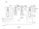
圖1是剖面側視圖,例示本揭露一些實施例之記憶體元件。FIG. 1 is a cross-sectional side view illustrating a memory device according to some embodiments of the present disclosure.
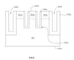
圖2是剖面側視圖,例示本揭露其他實施例之記憶體元件。FIG. 2 is a cross-sectional side view illustrating a memory device according to another embodiment of the present disclosure.
圖3是流程圖,例示本揭露一些實施例之記憶體元件的製備方法。FIG. 3 is a flowchart illustrating a method for fabricating a memory device according to some embodiments of the present disclosure.
圖4至圖20是剖視圖,例示本揭露一些實施例之記憶體元件的形成中間階段。4-20 are cross-sectional views illustrating intermediate stages in the formation of memory devices according to some embodiments of the present disclosure.
以下揭露內容提供許多不同的實施例,或實例,用於實現所提供主題的不同特徵。為了簡化本揭露內容,下面描述了元件和安排的具體例子。當然,這些只是例子,並不意旨是限制性的。例如,在接下來的描述中,第一特徵在第二特徵上的形成可以包括第一和第二特徵直接接觸的實施例,也可以包括在第一和第二特徵之間形成附加特徵的實施例,這樣第一和第二特徵可以不直接接觸。The following disclosure provides many different embodiments, or examples, for implementing different features of the presented subject matter. To simplify the present disclosure, specific examples of components and arrangements are described below. Of course, these are examples only and are not meant to be limiting. For example, in the description that follows, the formation of a first feature on a second feature may include an embodiment where the first and second features are in direct contact, or may include an embodiment where an additional feature is formed between the first and second features For example, such that the first and second features may not be in direct contact.
此外,本揭露內容可能會在各實施例中重複參考數字和/或字母。這種重複是為了簡單明瞭,其本身並不決定所討論的各種實施例和/或設置之間的關係。In addition, the present disclosure may repeat reference numerals and/or letters in various embodiments. This repetition is for clarity and does not in itself determine the relationship between the various embodiments and/or arrangements discussed.
此外,空間相對用語,如"下"、"下方"、"之下"、"上"、"上方"、"之上"等,為了便於描述,在此可用於描述一個元素或特徵與圖中所示的另一個(些)元素或特徵的關係。空間上的相對用語旨在包括元件在使用或操作中的不同方向,以及圖中描述的方向。該元件可以有其他方向(旋轉90度或其他方向),這裡使用的空間相對描述詞也同樣可以相應地解釋。In addition, spatially relative terms, such as "below", "under", "under", "upper", "above", "above", etc., may be used herein to describe an element or feature as compared to that in the drawings for ease of description. relationship to another element or feature shown. Spatially relative terms are intended to encompass different orientations of elements in use or operation, as well as the orientation depicted in the figures. The element may be otherwise oriented (rotated 90 degrees or otherwise) and the spatially relative descriptors used herein interpreted accordingly.
圖1是剖面側視圖,例示本揭露一些實施例之記憶體元件100。在一些實施例中,記憶體元件100包括以列(row)和行(column)排列的一些單元胞(unit cell)。FIG. 1 is a cross-sectional side view illustrating a
在一些實施例中,記憶體元件100包括半導體基底101。在一些實施例中,半導體基底101包括半導體材料,如矽、鍺、鎵、砷,或其組合。在一些實施例中,半導體基底101包括塊狀(bulk)半導體材料。在一些實施例中,半導體基底101是一半導體晶圓(例如,一矽晶圓)或一絕緣體上的半導體(semiconductor-on-insulator,SOI)晶圓(例如,一絕緣體上的矽晶圓)。在一些實施例中,半導體基底101是一矽基底。在一些實施例中,半導體基底101包括輕度摻雜的單晶矽。在一些實施例中,半導體基底101是一p型基底。In some embodiments, the
在一些實施例中,半導體基底101包括多個主動區(active area,AA)101a。主動區101a是半導體基底101中的一摻雜區域。在一些實施例中,主動區101a在半導體基底101的一頂面上方或下方水平延伸。在一些實施例中,每個主動區101a包括一相同類型的摻雜物。在一些實施例中,每個主動區101a包括的摻雜物類型與包括在其他主動區101a中的摻雜物類型不同。在一些實施例中,每個主動區101a具有一相同的導電類型。在一些實施例中,主動區101a包括一N型摻雜物。In some embodiments, the
在一些實施例中,半導體基底101包括第一表面101b和與第一表面101b相對的第二表面101c。在一些實施例中,第一表面101b是半導體基底101的一正(front)面,其中電子元件或組件(component)隨後在第一表面101b上方形成並經設置以與外部電路電連接。在一些實施例中,第二表面101c是半導體基底101的一背(back)面,其中沒有電子元件或組件。In some embodiments, the
在一些實施例中,半導體基底101包括延伸至半導體基底101的凹槽103a。在一些實施例中,凹槽103a從第一表面101b向半導體基底101的第二表面101c延伸。在一些實施例中,凹槽103a從第一表面101b向半導體基底101的第二表面101c逐漸變細。在一些實施例中,凹槽103a的一深度實質上大於主動區101a的一深度。In some embodiments, the
在一些實施例中,記憶體元件100包括設置在凹槽103a內的字元線120。在一些實施例中,字元線120包括第一絕緣層104、第一導電層105和第一導電構件107。在一些實施例中,第一絕緣層104與凹槽103a共形並設置於其中。在一些實施例中,第一導電層105由第一絕緣層104包圍。在一些實施例中,第一導電構件107由第一導電層105包圍。In some embodiments, the
在一些實施例中,第一絕緣層104沿著凹槽103a的整個側壁設置。在一些實施例中,第一絕緣層104包括一介電質材料,如氧化物。在一些實施例中,第一絕緣層104的製作技術是一絕緣材料,如氧化矽、氮化矽、氮氧化矽(silicon oxynitride)等,或其組合。在一些實施例中,第一絕緣層104包括具有一低介電常數(低k)的絕緣材料。In some embodiments, the first insulating
在一些實施例中,第一絕緣層104包括與凹槽103a共形的第一襯層部分104a和設置在第一導電層105之上的第一突出部分104b。在一些實施例中,第一襯層部分104a沿凹槽103a的整個側壁設置。在一些實施例中,第一襯層部分104a與第一突出部分104b耦合。在一些實施例中,第一突出部分104b從第一襯層部分104a中突出。In some embodiments, the first insulating
在一些實施例中,第一突出部分104b的厚度在大約2微米至大約3微米的範圍內。在一些實施例中,第一突出部分104b包括一低K介電質材料。在一些實施例中,第一襯層部分104a在大約4微米至6微米的範圍內。在一些實施例中,第一襯層部分104a的一厚度實質上大於第一突出部分104b的一厚度。In some embodiments, the thickness of the first protruding
在一些實施例中,第一襯層部分104a的一頂面104c和第一突出部分104b的一頂面104d透過半導體基底101曝露。在一些實施例中,第一襯層部分104a和第一突出部分104b包括一相同材料或一不同材料。在一些實施例中,第一襯層部分104a和第一突出部分104b是整體(integrally)形成。In some embodiments, a
在一些實施例中,第一導電層105設置在凹槽103a內並由第一絕緣層104包圍。在一些實施例中,第一導電層105由第一襯層部分104a包圍,並設置在第一突出部分104b下方。在一些實施例中,第一導電層105的頂面105a與第一突出部分104b接觸。在一些實施例中,第一導電層105的頂面105a實質上低於第一襯層部分104a的頂面104c和第一突出部分104b的頂面104d。在一些實施例中,第一導電層105包括一導電材料,如氮化鈦(TiN)。In some embodiments, the first
在一些實施例中,第一導電構件107經設置在第一導電層105內。第一導電構件107由第一襯層部分104a包圍。在一些實施例中,第一導電構件107經設置在半導體基底101的主動區101a下方。在一些實施例中,第一突出部分104b設置在第一導電構件107之上。在一些實施例中,第一導電構件107包括一導電材料,如鎢(W)。In some embodiments, the first
在一些實施例中,字元線120更包括設置在第一導電層105和第一導電構件107上方的第一功函數構件111,以及設置在第一功函數構件111上方的第一閘極絕緣構件113。在一些實施例中,第一功函數構件111和第一閘極絕緣構件113由第一絕緣層104包圍。在一些實施例中,第一功函數構件111和第一閘極絕緣構件113由第一突出部分104b包圍並與之接觸。在一些實施例中,第一功函數構件111與第一導電層105的頂面105a接觸。In some embodiments, the
在一些實施例中,第一導電層105和第一導電構件107的總寬度W1實質上等於第一突出部分104b和第一功函數構件111的總寬度W2。在一些實施例中,總寬度W1實質上等於第一突出部分104b和第一閘極絕緣構件113的總寬度W2。在一些實施例中,第一功函數構件111包括多晶矽(polysilicon)或多晶體矽(polycrystalline silicon)。在一些實施例中,第一功函數構件111具有一低功函數。在一些實施例中,第一功函數構件111具有雙重功函數,包括金屬和多晶矽。在一些實施例中,第一功函數構件111做為一閘極電極。In some embodiments, the total width W1 of the first
在一些實施例中,第一閘極絕緣構件113包括介電質材料,如氮化物。在一些實施例中,第一閘極絕緣構件113做為一閘極介電質。在一些實施例中,第一閘極絕緣構件113的一頂面與第一襯層部分104a的頂面104c和第一突出部分104b的頂面104d實質上共面。In some embodiments, the first
在一些實施例中,記憶體元件100更包括鄰近字元線120的隔離結構102。在一些實施例中,隔離結構102從第一表面101b向第二表面101c延伸至半導體基底101中。在一些實施例中,隔離結構102是一淺溝隔離(shallow trench isolation,STI)。在一些實施例中,隔離結構102定義主動區101a的一邊界。In some embodiments, the
在一些實施例中,隔離結構102包括第二襯層部分102a和從第二襯層部分102a橫向突出的第二突出部分102b。在一些實施例中,第二突出部分102b的厚度在大約2微米至大約3微米的範圍內。在一些實施例中,第二襯層部分102a和第二突出部分102b包括一相同材料或一不同材料。在一些實施例中,第二襯層部分102a和第二突出部分102b是整體形成。In some embodiments, the
在一些實施例中,隔離結構102的製作技術是一絕緣材料,如氧化矽、氮化矽、氮氧化矽等,或其組合。在一些實施例中,隔離結構102和第一絕緣層104包括一相同材料或一不同材料。在一些實施例中,隔離結構102的一寬度實質上大於字元線120的一寬度。在一些實施例中,隔離結構102的一深度實質上大於字元線120的一深度。In some embodiments, the fabrication technology of the
在一些實施例中,第二導電層106和第二導電構件108由隔離結構102的第二襯層部分102a包圍。在一些實施例中,第二導電構件108由第二導電層106包圍。在一些實施例中,第二導電層106和第二導電構件108經設置在第二突出部分102b下方。在一些實施例中,第二突出部分102b與第二導電層106接觸。In some embodiments, the second
在一些實施例中,第二導電層106包括一導電材料,如氮化鈦(TiN)。在一些實施例中,第二導電構件108包括一導電材料,如鎢(W)。在一些實施例中,第一導電層105和第二導電層106包括一相同材料或一不同材料。在一些實施例中,第一導電構件107和第二導電構件108包括一相同材料或一不同材料。In some embodiments, the second
在一些實施例中,在第二導電層106和第二導電構件108上方設置第二功函數構件112,在第二功函數構件112上方設置第二閘極絕緣構件114。在一些實施例中,第二功函數構件112和第二閘極絕緣構件114由隔離結構102包圍。在一些實施例中,第二功函數構件112和第二閘極絕緣構件114由第二突出部分102b包圍並與之接觸。在一些實施例中,第二功函數構件112與第二導電層106的頂面106a接觸。In some embodiments, a second
在一些實施例中,第二功函數構件112包括多晶矽或多晶體矽。在一些實施例中,第二功函數構件112具有一低功函數。在一些實施例中,第二功函數構件112具有雙重功函數,包括金屬和多晶矽。在一些實施例中,第二閘極絕緣構件114包括一介電質材料,如氮化物。In some embodiments, the second
在一些實施例中,第一功函數構件111和第二功函數構件112包括一相同材料或一不同材料。在一些實施例中,第一閘極絕緣構件113和第二閘極絕緣構件114包括一相同材料或一不同材料。在一些實施例中,第二閘極絕緣構件114的一頂面與第二襯層部分102a的頂面102c和第二突出部分102b的頂面102d實質上共面。In some embodiments, the first
由於第一絕緣層104的上部(圍繞第一功函數構件111的字元線120)與第一絕緣層104的下部(圍繞第一導電層105和第一功函數構件111下方的第一導電構件107)相比具有更大的厚度,因此可以抑制閘極引發汲極漏電流(gate-induced drain leakage,GIDL)。此外,圍繞第一導電層105和第一導電構件107的第一絕緣層104具有較小的厚度,因此可以改善對字元線120的操作控制。因此,記憶體元件100的性能可以獲得改善。Since the upper part of the first insulating layer 104 (surrounding the
圖2是剖面側視圖,例示本揭露一些實施例之記憶體元件200。記憶體元件200與記憶體元件100相似,只是在圖2中第一絕緣層104和隔離結構102內沒有介面。換句話說,如圖1所示的第一襯層部分104a和第一突出部分104b被整體形成,分別成為圖2所示的第一絕緣層104和隔離結構102。在一些實施例中,第一絕緣層104至少部分地設置在第一導電層105之上。FIG. 2 is a cross-sectional side view illustrating a
在一些實施例中,第一導電層105之上的第一絕緣層104的寬度W3實質上大於第一導電層105和第一導電構件107周圍的第一絕緣層104的寬度W4。在一些實施例中,第二導電層106之上的隔離結構102的寬度W5實質上大於第二導電層106和第二導電構件108周圍的隔離結構102的寬度W6。In some embodiments, the width W3 of the first insulating
圖3是流程圖,例示本揭露一些實施例之記憶體元件100或200的製備方法S300,圖4至圖20是剖視圖,例示本揭露一些實施例之記憶體元件100或200的形成中間階段。3 is a flow chart illustrating the method S300 for manufacturing the
在圖4至圖20例示的階段也可在圖3的流程圖中得到說明。在下面的討論中,圖4至圖20例示的製備階段為參照圖3之製程步驟進行討論。製備方法S300包括一些操作,描述和說明不旨為對操作順序的限制。製備方法S300包括一些步驟(S301、S302、S303、S304、S305、S306和S307)。The stages illustrated in FIGS. 4 to 20 are also illustrated in the flowchart of FIG. 3 . In the following discussion, the fabrication stages illustrated in FIGS. 4-20 are discussed with reference to the process steps of FIG. 3 . The preparation method S300 includes some operations, and the description and illustration are not intended to limit the sequence of operations. The preparation method S300 includes some steps (S301, S302, S303, S304, S305, S306 and S307).
參照圖4和圖5,根據圖3中的步驟S301提供半導體基底101。圖4是例示半導體基底101的剖視俯視圖,圖5是例示沿圖4中A-A'線拍攝的半導體基底101的剖視圖。在一些實施例中,半導體基底101經定義以具有主動區101a,並包括圍繞主動區101a的隔離層102e。在一些實施例中,隔離層102e從半導體基底101的第一表面101b向第二表面101c延伸。在一些實施例中,隔離層102e包括一介電質材料,如氧化物或類似物。Referring to FIGS. 4 and 5 , a
參照圖6和圖7,根據圖3中的步驟S302,形成延伸至半導體基底101的第一凹槽103a。圖6是例示半導體基底101的剖視俯視圖,圖7是例示沿圖6中B-B'線拍攝的半導體基底101的剖視圖。在一些實施例中,在半導體基底101的第一表面101b上形成一些溝槽103。溝槽103穿過主動區101a或隔離層102e(如圖4和圖5所示)延伸。Referring to FIGS. 6 and 7 , according to step S302 in FIG. 3 , a
在一些實施例中,溝槽103的形成包括第一凹槽103a的形成和第二凹槽103b的形成。在一些實施例中,第一凹槽103a的形成和第二凹槽103b的形成分別或同時進行。在一些實施例中,第一凹槽103a的形成包括去除半導體基底101的一些部分。在一些實施例中,第二凹槽103b的形成包括去除隔離層102e的一些部分。In some embodiments, the formation of the
在一些實施例中,第一凹槽103a穿過主動區101a延伸,而第二凹槽103b穿過隔離層102e延伸。在一些實施例中,第一凹槽103a和第二凹槽103b從第一表面101b向半導體基底101的第二表面101c延伸。在一些實施例中,在形成第二凹槽103b之後形成第二襯層部分102a。In some embodiments, the
參照圖8,根據圖3中的步驟S303,形成與第一凹槽103a共形的第一絕緣層104的第一襯層部分104a。在一些實施例中,第一襯層部分104a經設置在第一凹槽103a內。在一些實施例中,第一襯層部分104a是藉由沉積、氧化或任何其他合適的製程形成。在一些實施例中,第一襯層部分104a包括氧化物。Referring to FIG. 8, according to step S303 in FIG. 3, the
參照圖9和圖10,根據圖3中的步驟S304,設置與第一襯層部分104a共形的第一導電材料105b。在一些實施例中,如圖9所示,在半導體基底101上方設置導電材料125,並由第一襯層部分104a和第二襯層部分102a包圍,然後去除導電材料125的一些部分,以形成第一導電材料105b和第二導電材料106b,如圖10所示。Referring to FIGS. 9 and 10 , according to step S304 in FIG. 3 , a first
在一些實施例中,第一導電材料105b和第二導電材料106b是藉由沉積或任何其他合適的製程分別或同時設置。在一些實施例中,第一導電材料105b和第二導電材料106b包括氮化鈦(TiN)。在一些實施例中,第一導電材料105b和第二導電材料106b分別與第一襯層部分104a和第二襯層部分102a共形。In some embodiments, the first
參照圖11和圖12,根據圖3中的步驟S305,形成由第一導電材料105b包圍的第一導電構件107。第一導電構件107設置在第一凹槽103a內,並由第一襯層部分104a和第一導電材料105b包圍。在一些實施例中,第一導電構件107是藉由設置被第一導電材料105b包圍的第三導電材料107a而形成,如圖11所示,然後去除第三導電材料107a的一部分,成為第一導電構件107,如圖12所示。11 and 12, according to step S305 in FIG. 3, the first
在一些實施例中,第三導電材料107a是藉由沉積或任何其他合適的製程來設置。在一些實施例中,第三導電材料107a的該部分是藉由蝕刻或任何其他合適的製程而去除。在一些實施例中,第三導電材料107a包括鎢(W)。In some embodiments, the third
在一些實施例中,還形成由第二導電材料106b包圍的第二導電構件108。第二導電構件108設置在第二凹槽103b內,並由第二襯層部分102a和第二導電材料106b包圍。在一些實施例中,第二導電構件108是藉由設置被第二導電材料106b包圍的第四導電材料108a而形成,如圖11所示,然後去除第四導電材料108a的一部分,成為第二導電構件108,如圖12所示。In some embodiments, a second
在一些實施例中,第四導電材料108a是藉由沉積或任何其他合適的製程來設置。在一些實施例中,第四導電材料108a的該部分是藉由蝕刻或任何其他合適的製程而去除。在一些實施例中,第四導電材料108a包括鎢(W)。在一些實施例中,第一導電構件107的形成和第二導電構件108的形成分別或同時進行。In some embodiments, the fourth
參照圖13和圖14,根據圖3中的步驟S306,第五導電材料105c經設置在第一導電構件107上方,以形成包圍第一導電構件107的第一導電層105。在一些實施例中,第五導電材料105c藉由沉積或任何其他合適的製程來設置在第一導電構件107上。在一些實施例中,第五導電材料105c和第一導電材料105b是一相同材料。在一些實施例中,第五導電材料105c包括氮化鈦(TiN)。13 and 14, according to step S306 in FIG. In some embodiments, the fifth
在一些實施例中,在設置如圖13所示的第五導電材料105c後,第一導電材料105b的一部分被移除,以形成如圖14所示的第一導電層105。在一些實施例中,第一導電材料105b的該部分是藉由蝕刻、清洗或任何其他合適的製程而去除。In some embodiments, after disposing the fifth
在一些實施例中,第六導電材料106c藉由沉積或任何其他合適的製程來設置在第二導電構件108上。在一些實施例中,第六導電材料106c和第二導電材料106b是一相同材料。在一些實施例中,第六導電材料106c包括氮化鈦(TiN)。在一些實施例中,第一導電材料105b、第五導電材料105c、第二導電材料106b和第六導電材料106c是相同的材料。在一些實施例中,第五導電材料105c的設置和第六導電材料106c的設置分別或同時執行。In some embodiments, the sixth
在一些實施例中,在設置如圖13所示的第六導電材料106c後,第二導電材料106b的一部分被移除,以形成如圖14所示的第二導電層106。在一些實施例中,第二導電材料106b的該部分是藉由蝕刻、清洗或任何其他合適的製程而去除。在一些實施例中,第一導電材料105b的該部分的去除和第二導電材料106b的該部分的去除是分別或同時執行。In some embodiments, after disposing the sixth
參照圖15和圖16,根據圖3中的步驟S307,在第一導電層105和第一導電構件107之上的第一絕緣層104的第一突出部分104b被形成。在一些實施例中,第一突出部分104b的形成包括在半導體基底101、第一襯層部分104a、第一導電層105和第一導電構件107上方設置絕緣材料124。在一些實施例中,絕緣材料124是藉由原子層沉積(ALD)或任何其他合適的製程來設置。15 and 16, according to step S307 in FIG. 3, the first protruding
在一些實施例中,在如圖15所示的設置絕緣材料124之後,設置在半導體基底101和第一襯層部分104a上方的絕緣材料124的一部分被移除,以形成第一突出部分104b。在一些實施例中,絕緣材料124的該部分是藉由非等向性蝕刻、平坦化或任何其他合適的製程而去除。第一突出部分104b設置在第一導電層105上和第一導電構件107之上。In some embodiments, after disposing the insulating
在一些實施例中,還形成隔離結構102在第二導電層106和第二導電構件108之上的第二突出部分102b。在一些實施例中,第二突出部分102b的形成包括將絕緣材料124設置在半導體基底101、第二襯層部分102a、第二導電層106和第二導電構件108上方,如圖15所示,然後去除設置在半導體基底101和第二襯層部分102a上方的絕緣材料124的一部分,以形成第二突出部分102b,如圖16所示。第二突出部分102b設置在第二導電層106上並在第二導電構件108之上。在一些實施例中,第一突出部分104b的形成和第二突出部分102b的形成分別或同時執行。In some embodiments, a second protruding
參照圖17和圖18,在第一導電層105上方並由第一突出部分104b包圍的第一功函數構件111被形成。在一些實施例中,如圖17所示,第一功函數構件111是藉由設置被第一突出部分104b包圍的第一功函數材料111a,然後去除第一功函數材料111a的一部分以形成如圖18所示的第一功函數構件111。在一些實施例中,第一功函數材料111a是藉由沉積、CVD或任何其他合適的製程來設置。在一些實施例中,第一功函數材料111a的該部分是藉由蝕刻或任何其他合適的製程而去除。Referring to FIGS. 17 and 18 , a first
在一些實施例中,第二功函數構件112是藉由設置被第二突出部分102b包圍的第二功函數材料112a而形成,如圖17所示,然後去除第二功函數材料112a的一部分以形成第二功函數構件112,如圖18所示。在一些實施例中,第二功函數材料112a是藉由沉積、CVD或任何其他合適的製程來設置。在一些實施例中,第二功函數材料112a的該部分是藉由蝕刻或任何其他合適的製程而去除。In some embodiments, the second
在一些實施例中,第一功函數材料111a的設置和第二功函數材料112a的設置分別或同時執行。在一些實施例中,第一功函數材料111a和第二功函數材料112a是相同的材料。在一些實施例中,第一功函數材料111a和第二功函數材料112a包括多晶矽。In some embodiments, the disposition of the first
參照圖19,在第一功函數構件111上方形成第一閘極絕緣構件113,並由第一突出部分104b包圍。在一些實施例中,第一閘極絕緣構件113的形成包括藉由沉積或任何其他合適的製程來設置一閘極絕緣材料。在一些實施例中,在第二功函數構件112上方形成第二閘極絕緣構件114,並由第二突出部分102b包圍。在一些實施例中,第一閘極絕緣構件113的形成和第二閘極絕緣構件114的形成分別或同時執行。在一些實施例中,圖1的記憶體元件100如圖19所示形成。在一些實施例中,圖2的記憶體元件200如圖20所示形成。Referring to FIG. 19 , a first
在本揭露的一個實施例提供一種記憶體元件。該記憶體元件包括一半導體基底,其定義有一主動區並包括延伸至該半導體基底中的一凹槽;以及設置在該凹槽內的一字元線,其中該字元線包括設置在該凹槽內的一絕緣層、由該絕緣層包圍的一導電層,以及由該導電層包圍的一導電構件,並且該絕緣層包括與該凹槽共形的一襯層部分和設置在該導電層之上的一突出部分。An embodiment of the present disclosure provides a memory device. The memory element includes a semiconductor substrate, which defines an active area and includes a groove extending into the semiconductor substrate; and a word line arranged in the groove, wherein the word line includes an An insulating layer in the groove, a conductive layer surrounded by the insulating layer, and a conductive member surrounded by the conductive layer, and the insulating layer includes a liner portion conformal to the groove and disposed on the conductive layer a protruding part above.
在本揭露的另一個實施例提供一種記憶體元件。該記憶體元件包括一半導體基底,其定義有一主動區並包括延伸至該半導體基底中的一第一凹槽;以及設置在該第一凹槽內的一字元線,其中該字元線包括設置在該第一凹槽內的一第一絕緣層,由該第一絕緣層包圍的一第一導電層,以及由該第一導電層包圍的一第一導電構件,並且該第一絕緣層至少部分地設置在該第一導電層之上。Another embodiment of the present disclosure provides a memory device. The memory element includes a semiconductor substrate defining an active area and including a first groove extending into the semiconductor substrate; and a word line disposed in the first groove, wherein the word line includes a first insulating layer disposed in the first groove, a first conductive layer surrounded by the first insulating layer, and a first conductive member surrounded by the first conductive layer, and the first insulating layer at least partially disposed on the first conductive layer.
在本揭露的另一個實施例提供一種記憶體元件的製備方法。該製備方法包括以下步驟:提供一半導體基底,其定義有一主動區並包括圍繞該主動區的一隔離層;形成延伸至半導體基底中並穿過該主動區的一第一凹槽;形成與該第一凹槽共形的一第一絕緣層的一第一襯墊部分;將一第一導電材料共形設置到該第一襯墊部分;形成由該第一導電材料包圍的一第一導電構件;在該第一導電構件上方設置一第二導電材料,以形成包圍該第一導電構件的一第一導電層;以及在該第一導電層和該第一導電構件之上形成該第一絕緣層的一第一突出部分。Another embodiment of the present disclosure provides a method for manufacturing a memory device. The preparation method includes the following steps: providing a semiconductor substrate, which defines an active region and includes an isolation layer surrounding the active region; forming a first groove extending into the semiconductor substrate and passing through the active region; A first liner portion of a first insulating layer conformal to the first recess; conformally disposing a first conductive material to the first liner portion; forming a first conductive layer surrounded by the first conductive material member; a second conductive material is disposed above the first conductive member,forming a first conductive layer surrounding the first conductive member; and forming a first protruding portion of the first insulating layer on the first conductive layer and the first conductive member.
總之,由於圍繞功函數構件的字元線的絕緣層與圍繞功函數構件下的導電構件的絕緣層相比具有更大的厚度,因此可以抑制閘極引發汲極漏電流(GIDL)。此外,圍繞導電構件的絕緣層具有較小的厚度,因此可以改善對字元線的操作控制。因此,記憶體元件的性能和記憶體元件的製造過程獲得了改善。雖然已詳述本揭露及其優點,然而應理解可以進行其他變化、取代與替代而不脫離揭露專利範圍所定義之本揭露的精神與範圍。例如,可用不同的方法實施上述的許多製程,並且以其他製程或其組合替代上述的許多製程。In conclusion, since the insulating layer surrounding the word line of the work function member has a greater thickness than the insulating layer surrounding the conductive member under the work function member, gate induced drain leakage (GIDL) can be suppressed. In addition, the insulating layer surrounding the conductive member has a smaller thickness, so that the operation control of the word line can be improved. Therefore, the performance of the memory device and the manufacturing process of the memory device are improved. Although the present disclosure and its advantages have been described in detail, it should be understood that other changes, substitutions and substitutions can be made hereto without departing from the spirit and scope of the present disclosure as defined by the patent claims disclosed. For example, many of the processes described above can be performed in different ways and replaced by other processes or combinations thereof.
再者,本揭露案的範圍並不受限於說明書中所述之製程、機械、製造、物質組成物、手段、方法與步驟之特定實施例。該技藝之技術人士可自本揭露的揭示內容理解以根據本揭露而使用與本文所述之對應實施例具有相同功能或是達到實質上相同結果之現存或是未來發展之製程、機械、製造、物質組成物、手段、方法、或步驟。據此,此等製程、機械、製造、物質組成物、手段、方法、或步驟係包括於本揭露案之揭露專利範圍內。Furthermore, the scope of the disclosure is not limited to the particular embodiments of the process, machine, manufacture, composition of matter, means, methods and steps described in the specification. Those skilled in the art can understand from the disclosure content of this disclosure that they can use existing or future developed processes, machinery, manufacturing, A composition of matter, means, method, or step. Accordingly, such processes, machinery, manufacture, material composition, means, methods, or steps are included in the scope of the patent disclosure of this disclosure.
100:記憶體元件100: memory components
101:半導體基底101:Semiconductor substrate
101a:主動區101a: Active area
101b:第一表面101b: first surface
101c:第二表面101c: Second Surface
102:隔離結構102: Isolation structure
102a:第二襯層部分102a: second liner part
102b:第二突出部分102b: Second protrusion
102c:頂面102c: top surface
102d:頂面102d: top surface
103a:凹槽(第一凹槽)103a: groove (first groove)
104:第一絕緣層104: The first insulating layer
104a:第一襯層部分104a: first lining part
104b:第一突出部分104b: first protrusion
104c:頂面104c: top surface
104d:頂面104d: top surface
105:第一導電層105: the first conductive layer
105a:頂面105a: top surface
106:第二導電層106: the second conductive layer
106a:頂面106a: top surface
107:第一導電構件107: first conductive member
108:第二導電構件108: second conductive member
111:第一功函數構件111: The first work function component
112:第二功函數構件112: Second work function component
113:第一閘極絕緣構件113: the first gate insulating member
114:第二閘極絕緣構件114: second gate insulating member
120:字元線120: character line
W1:總寬度W1: total width
W2:總寬度W2: total width
Claims (39)
Translated fromChineseApplications Claiming Priority (4)
| Application Number | Priority Date | Filing Date | Title |
|---|---|---|---|
| US17/552,736US11832432B2 (en) | 2021-12-16 | 2021-12-16 | Method of manufacturing memory device having word lines with reduced leakage |
| US17/552,736 | 2021-12-16 | ||
| US17/552,882 | 2021-12-16 | ||
| US17/552,882US20230197771A1 (en) | 2021-12-16 | 2021-12-16 | Memory device having word lines with reduced leakage |
Publications (2)
| Publication Number | Publication Date |
|---|---|
| TWI803217Btrue TWI803217B (en) | 2023-05-21 |
| TW202327032A TW202327032A (en) | 2023-07-01 |
Family
ID=86744126
Family Applications (1)
| Application Number | Title | Priority Date | Filing Date |
|---|---|---|---|
| TW111107763ATWI803217B (en) | 2021-12-16 | 2022-03-03 | Memory device having word lines with reduced leakage |
Country Status (2)
| Country | Link |
|---|---|
| CN (1) | CN116266575A (en) |
| TW (1) | TWI803217B (en) |
Citations (4)
| Publication number | Priority date | Publication date | Assignee | Title |
|---|---|---|---|---|
| TW201715702A (en)* | 2015-10-29 | 2017-05-01 | 華邦電子股份有限公司 | Memory device and method of manufacturing the same |
| TW201906089A (en)* | 2017-06-22 | 2019-02-01 | 華邦電子股份有限公司 | Dynamic random access memory and method of fabricating the same |
| US20190067278A1 (en)* | 2017-08-28 | 2019-02-28 | Samsung Electronics Co., Ltd. | Semiconductor device including a gate insulation pattern and a gate electrode pattern |
| TW202141759A (en)* | 2020-04-16 | 2021-11-01 | 南亞科技股份有限公司 | Semiconductor memory device with air gaps between conductive features and method for preparing the same |
Family Cites Families (5)
| Publication number | Priority date | Publication date | Assignee | Title |
|---|---|---|---|---|
| GB0010041D0 (en)* | 2000-04-26 | 2000-06-14 | Koninkl Philips Electronics Nv | Trench semiconductor device manufacture |
| KR101110437B1 (en)* | 2010-01-25 | 2012-02-24 | 주식회사 하이닉스반도체 | Semiconductor Device and Method for Manufacturing the same |
| KR20150090669A (en)* | 2014-01-29 | 2015-08-06 | 에스케이하이닉스 주식회사 | Dual work function bruied gate type transistor, method for manufacturing the same and electronic device having the same |
| KR102511942B1 (en)* | 2016-12-16 | 2023-03-23 | 에스케이하이닉스 주식회사 | Semiconductor device having buried gate structure and method for manufacturing the same |
| KR102471277B1 (en)* | 2018-09-19 | 2022-11-28 | 삼성전자주식회사 | Semiconductor device having gate insulating layer |
- 2022
- 2022-03-03TWTW111107763Apatent/TWI803217B/enactive
- 2022-07-11CNCN202210811607.2Apatent/CN116266575A/enactivePending
Patent Citations (4)
| Publication number | Priority date | Publication date | Assignee | Title |
|---|---|---|---|---|
| TW201715702A (en)* | 2015-10-29 | 2017-05-01 | 華邦電子股份有限公司 | Memory device and method of manufacturing the same |
| TW201906089A (en)* | 2017-06-22 | 2019-02-01 | 華邦電子股份有限公司 | Dynamic random access memory and method of fabricating the same |
| US20190067278A1 (en)* | 2017-08-28 | 2019-02-28 | Samsung Electronics Co., Ltd. | Semiconductor device including a gate insulation pattern and a gate electrode pattern |
| TW202141759A (en)* | 2020-04-16 | 2021-11-01 | 南亞科技股份有限公司 | Semiconductor memory device with air gaps between conductive features and method for preparing the same |
Also Published As
| Publication number | Publication date |
|---|---|
| TW202327032A (en) | 2023-07-01 |
| CN116266575A (en) | 2023-06-20 |
Similar Documents
| Publication | Publication Date | Title |
|---|---|---|
| US6297090B1 (en) | Method for fabricating a high-density semiconductor memory device | |
| CN113644072B (en) | Semiconductor element structure and preparation method thereof | |
| US9859432B2 (en) | Semiconductor devices having spacer protection pattern | |
| US11139306B2 (en) | Memory device and method for fabricating the same | |
| KR20150090666A (en) | Dual work function bruied gate type transistor, method for manufacturing the same and electronic device having the same | |
| US8841716B2 (en) | Retrograde substrate for deep trench capacitors | |
| US6380589B1 (en) | Semiconductor-on-insulator (SOI) tunneling junction transistor SRAM cell | |
| US11832432B2 (en) | Method of manufacturing memory device having word lines with reduced leakage | |
| US20120286357A1 (en) | Sense-amp transistor of semiconductor device and method for manufacturing the same | |
| US20230197771A1 (en) | Memory device having word lines with reduced leakage | |
| JP2000174225A (en) | Semiconductor integrated circuit device and method of manufacturing the same | |
| TWI803217B (en) | Memory device having word lines with reduced leakage | |
| TWI794055B (en) | Memory device having word lines with improved resistance and manufacturing method thereof | |
| US11895820B2 (en) | Method of manufacturing memory device having word line with improved adhesion between work function member and conductive layer | |
| CN116782634A (en) | memory element | |
| US10204914B2 (en) | Method for fabricating semiconductor device | |
| TWI833234B (en) | Memory device having word line | |
| JP2008016636A (en) | Semiconductor device and manufacturing method thereof | |
| CN101136364A (en) | Semiconductor device and method for manufacturing dynamic random access memory | |
| US20230232613A1 (en) | Memory device having word line with improved adhesion between work function member and conductive layer | |
| US20230009397A1 (en) | Dynamic random access memory and method of manufacturing the same | |
| TWI825736B (en) | Method for preparing memory device | |
| CN110707086B (en) | Semiconductor device with a plurality of semiconductor chips | |
| TW202425755A (en) | Memory device having ultra-lightly doped region | |
| TW202301638A (en) | Dynamic random access memory and method of manufacturing the same |