TWI801631B - Semiconductor device manufacturing method and semiconductor device - Google Patents
Semiconductor device manufacturing method and semiconductor deviceDownload PDFInfo
- Publication number
- TWI801631B TWI801631BTW108125489ATW108125489ATWI801631BTW I801631 BTWI801631 BTW I801631BTW 108125489 ATW108125489 ATW 108125489ATW 108125489 ATW108125489 ATW 108125489ATW I801631 BTWI801631 BTW I801631B
- Authority
- TW
- Taiwan
- Prior art keywords
- conductive
- dielectric layer
- layer
- dielectric
- opening
- Prior art date
Links
- 239000004065semiconductorSubstances0.000titleclaimsabstractdescription62
- 238000004519manufacturing processMethods0.000titleclaimsdescription6
- 239000000758substrateSubstances0.000claimsabstractdescription47
- 239000000463materialSubstances0.000claimsdescription102
- 238000000151depositionMethods0.000claimsdescription84
- 239000004020conductorSubstances0.000claimsdescription82
- 150000004820halidesChemical class0.000claimsdescription57
- XKRFYHLGVUSROY-UHFFFAOYSA-NArgonChemical group[Ar]XKRFYHLGVUSROY-UHFFFAOYSA-N0.000claimsdescription42
- 238000005530etchingMethods0.000claimsdescription34
- 239000000126substanceSubstances0.000claimsdescription22
- XUIMIQQOPSSXEZ-UHFFFAOYSA-NSiliconChemical compound[Si]XUIMIQQOPSSXEZ-UHFFFAOYSA-N0.000claimsdescription21
- 229910052786argonInorganic materials0.000claimsdescription21
- 229910052710siliconInorganic materials0.000claimsdescription21
- 239000010703siliconSubstances0.000claimsdescription21
- 230000004888barrier functionEffects0.000claimsdescription20
- 238000002791soakingMethods0.000claimsdescription19
- OKTJSMMVPCPJKN-UHFFFAOYSA-NCarbonChemical compound[C]OKTJSMMVPCPJKN-UHFFFAOYSA-N0.000claimsdescription10
- 229910052799carbonInorganic materials0.000claimsdescription10
- IJGRMHOSHXDMSA-UHFFFAOYSA-NAtomic nitrogenChemical compoundN#NIJGRMHOSHXDMSA-UHFFFAOYSA-N0.000claimsdescription7
- 238000009792diffusion processMethods0.000claimsdescription7
- 229910052732germaniumInorganic materials0.000claimsdescription4
- GNPVGFCGXDBREM-UHFFFAOYSA-Ngermanium atomChemical compound[Ge]GNPVGFCGXDBREM-UHFFFAOYSA-N0.000claimsdescription4
- 229910052757nitrogenInorganic materials0.000claimsdescription3
- 238000000034methodMethods0.000abstractdescription132
- 230000006911nucleationEffects0.000abstractdescription49
- 238000010899nucleationMethods0.000abstractdescription49
- 238000011282treatmentMethods0.000abstractdescription47
- 230000009977dual effectEffects0.000abstractdescription5
- 239000010410layerSubstances0.000description279
- 230000008569processEffects0.000description83
- 230000008021depositionEffects0.000description41
- 241000894007speciesSpecies0.000description40
- 229910052751metalInorganic materials0.000description35
- 239000002184metalSubstances0.000description35
- 238000009832plasma treatmentMethods0.000description35
- 238000004140cleaningMethods0.000description30
- 239000007789gasSubstances0.000description29
- 238000005229chemical vapour depositionMethods0.000description20
- 239000002243precursorSubstances0.000description17
- 229910052721tungstenInorganic materials0.000description16
- WFKWXMTUELFFGS-UHFFFAOYSA-NtungstenChemical compound[W]WFKWXMTUELFFGS-UHFFFAOYSA-N0.000description15
- 239000010937tungstenSubstances0.000description15
- UFHFLCQGNIYNRP-UHFFFAOYSA-NHydrogenChemical compound[H][H]UFHFLCQGNIYNRP-UHFFFAOYSA-N0.000description13
- 239000001257hydrogenSubstances0.000description13
- 229910052739hydrogenInorganic materials0.000description13
- 239000012159carrier gasSubstances0.000description12
- 238000004544sputter depositionMethods0.000description11
- 150000001875compoundsChemical class0.000description10
- 229920002120photoresistant polymerPolymers0.000description10
- 229910017052cobaltInorganic materials0.000description9
- 239000010941cobaltSubstances0.000description9
- GUTLYIVDDKVIGB-UHFFFAOYSA-Ncobalt atomChemical compound[Co]GUTLYIVDDKVIGB-UHFFFAOYSA-N0.000description9
- FAQYAMRNWDIXMY-UHFFFAOYSA-NtrichloroboraneChemical compoundClB(Cl)ClFAQYAMRNWDIXMY-UHFFFAOYSA-N0.000description9
- HMDDXIMCDZRSNE-UHFFFAOYSA-N[C].[Si]Chemical compound[C].[Si]HMDDXIMCDZRSNE-UHFFFAOYSA-N0.000description8
- 230000004048modificationEffects0.000description8
- 238000012986modificationMethods0.000description8
- 239000003638chemical reducing agentSubstances0.000description7
- 239000003795chemical substances by applicationSubstances0.000description7
- 150000002431hydrogenChemical class0.000description7
- 238000005468ion implantationMethods0.000description7
- 239000004215Carbon black (E152)Substances0.000description6
- KJTLSVCANCCWHF-UHFFFAOYSA-NRutheniumChemical compound[Ru]KJTLSVCANCCWHF-UHFFFAOYSA-N0.000description6
- 238000000231atomic layer depositionMethods0.000description6
- 230000015572biosynthetic processEffects0.000description6
- 229930195733hydrocarbonNatural products0.000description6
- 150000002430hydrocarbonsChemical class0.000description6
- 239000011229interlayerSubstances0.000description6
- 238000000623plasma-assisted chemical vapour depositionMethods0.000description6
- 229910052707rutheniumInorganic materials0.000description6
- PXHVJJICTQNCMI-UHFFFAOYSA-NNickelChemical compound[Ni]PXHVJJICTQNCMI-UHFFFAOYSA-N0.000description5
- 229910052581Si3N4Inorganic materials0.000description5
- 125000004429atomChemical group0.000description5
- 230000008901benefitEffects0.000description5
- 239000005380borophosphosilicate glassSubstances0.000description5
- IJOOHPMOJXWVHK-UHFFFAOYSA-NchlorotrimethylsilaneChemical compoundC[Si](C)(C)ClIJOOHPMOJXWVHK-UHFFFAOYSA-N0.000description5
- 150000001247metal acetylidesChemical class0.000description5
- 239000005360phosphosilicate glassSubstances0.000description5
- 238000001020plasma etchingMethods0.000description5
- 230000009467reductionEffects0.000description5
- 229910021332silicideInorganic materials0.000description5
- HQVNEWCFYHHQES-UHFFFAOYSA-Nsilicon nitrideChemical compoundN12[Si]34N5[Si]62N3[Si]51N64HQVNEWCFYHHQES-UHFFFAOYSA-N0.000description5
- 238000004528spin coatingMethods0.000description5
- ZOKXTWBITQBERF-UHFFFAOYSA-NMolybdenumChemical compound[Mo]ZOKXTWBITQBERF-UHFFFAOYSA-N0.000description4
- VYPSYNLAJGMNEJ-UHFFFAOYSA-NSilicium dioxideChemical compoundO=[Si]=OVYPSYNLAJGMNEJ-UHFFFAOYSA-N0.000description4
- 239000003575carbonaceous materialSubstances0.000description4
- 239000002131composite materialSubstances0.000description4
- 238000005137deposition processMethods0.000description4
- -1dimethylsiloxaneChemical class0.000description4
- 238000005516engineering processMethods0.000description4
- 229940104869fluorosilicateDrugs0.000description4
- 239000011521glassSubstances0.000description4
- FFUAGWLWBBFQJT-UHFFFAOYSA-NhexamethyldisilazaneChemical compoundC[Si](C)(C)N[Si](C)(C)CFFUAGWLWBBFQJT-UHFFFAOYSA-N0.000description4
- 239000007943implantSubstances0.000description4
- 238000002513implantationMethods0.000description4
- 229910052750molybdenumInorganic materials0.000description4
- 239000011733molybdenumSubstances0.000description4
- 229910052814silicon oxideInorganic materials0.000description4
- 229910052724xenonInorganic materials0.000description4
- FHNFHKCVQCLJFQ-UHFFFAOYSA-Nxenon atomChemical compound[Xe]FHNFHKCVQCLJFQ-UHFFFAOYSA-N0.000description4
- GJWAPAVRQYYSTK-UHFFFAOYSA-N[(dimethyl-$l^{3}-silanyl)amino]-dimethylsiliconChemical compoundC[Si](C)N[Si](C)CGJWAPAVRQYYSTK-UHFFFAOYSA-N0.000description3
- YGTSMYMNDOTCEI-UHFFFAOYSA-N[W].FOFChemical compound[W].FOFYGTSMYMNDOTCEI-UHFFFAOYSA-N0.000description3
- 239000003989dielectric materialSubstances0.000description3
- 230000005669field effectEffects0.000description3
- 238000011049fillingMethods0.000description3
- 238000009616inductively coupled plasmaMethods0.000description3
- KAHVZNKZQFSBFW-UHFFFAOYSA-Nn-methyl-n-trimethylsilylmethanamineChemical compoundCN(C)[Si](C)(C)CKAHVZNKZQFSBFW-UHFFFAOYSA-N0.000description3
- 229910052754neonInorganic materials0.000description3
- GKAOGPIIYCISHV-UHFFFAOYSA-Nneon atomChemical compound[Ne]GKAOGPIIYCISHV-UHFFFAOYSA-N0.000description3
- 230000007935neutral effectEffects0.000description3
- 238000007747platingMethods0.000description3
- FVBUAEGBCNSCDD-UHFFFAOYSA-Nsilicide(4-)Chemical compound[Si-4]FVBUAEGBCNSCDD-UHFFFAOYSA-N0.000description3
- LIVNPJMFVYWSIS-UHFFFAOYSA-Nsilicon monoxideChemical compound[Si-]#[O+]LIVNPJMFVYWSIS-UHFFFAOYSA-N0.000description3
- 238000001179sorption measurementMethods0.000description3
- NXHILIPIEUBEPD-UHFFFAOYSA-Htungsten hexafluorideChemical compoundF[W](F)(F)(F)(F)FNXHILIPIEUBEPD-UHFFFAOYSA-H0.000description3
- 229910015844BCl3Inorganic materials0.000description2
- KRHYYFGTRYWZRS-UHFFFAOYSA-NFluoraneChemical compoundFKRHYYFGTRYWZRS-UHFFFAOYSA-N0.000description2
- 238000003302UV-light treatmentMethods0.000description2
- 239000012790adhesive layerSubstances0.000description2
- 238000004380ashingMethods0.000description2
- YGHUUVGIRWMJGE-UHFFFAOYSA-NchlorodimethylsilaneChemical compoundC[SiH](C)ClYGHUUVGIRWMJGE-UHFFFAOYSA-N0.000description2
- 238000004581coalescenceMethods0.000description2
- 239000010949copperSubstances0.000description2
- 230000003247decreasing effectEffects0.000description2
- 238000007772electroless platingMethods0.000description2
- 230000006870functionEffects0.000description2
- 230000002209hydrophobic effectEffects0.000description2
- 238000007654immersionMethods0.000description2
- 230000005499meniscusEffects0.000description2
- 229910052759nickelInorganic materials0.000description2
- 150000004767nitridesChemical class0.000description2
- QGLKJKCYBOYXKC-UHFFFAOYSA-NnonaoxidotritungstenChemical compoundO=[W]1(=O)O[W](=O)(=O)O[W](=O)(=O)O1QGLKJKCYBOYXKC-UHFFFAOYSA-N0.000description2
- 239000002245particleSubstances0.000description2
- 239000012071phaseSubstances0.000description2
- 239000002356single layerSubstances0.000description2
- SIOVKLKJSOKLIF-HJWRWDBZSA-Ntrimethylsilyl (1z)-n-trimethylsilylethanimidateChemical compoundC[Si](C)(C)OC(/C)=N\[Si](C)(C)CSIOVKLKJSOKLIF-HJWRWDBZSA-N0.000description2
- 229910001930tungsten oxideInorganic materials0.000description2
- PPWNCLVNXGCGAF-UHFFFAOYSA-N3,3-dimethylbut-1-yneChemical groupCC(C)(C)C#CPPWNCLVNXGCGAF-UHFFFAOYSA-N0.000description1
- ZOXJGFHDIHLPTG-UHFFFAOYSA-NBoronChemical compound[B]ZOXJGFHDIHLPTG-UHFFFAOYSA-N0.000description1
- 241001342895ChorusSpecies0.000description1
- RYGMFSIKBFXOCR-UHFFFAOYSA-NCopperChemical compound[Cu]RYGMFSIKBFXOCR-UHFFFAOYSA-N0.000description1
- KRHYYFGTRYWZRS-UHFFFAOYSA-MFluoride anionChemical compound[F-]KRHYYFGTRYWZRS-UHFFFAOYSA-M0.000description1
- MHAJPDPJQMAIIY-UHFFFAOYSA-NHydrogen peroxideChemical compoundOOMHAJPDPJQMAIIY-UHFFFAOYSA-N0.000description1
- 229910008484TiSiInorganic materials0.000description1
- RTAQQCXQSZGOHL-UHFFFAOYSA-NTitaniumChemical compound[Ti]RTAQQCXQSZGOHL-UHFFFAOYSA-N0.000description1
- NRTOMJZYCJJWKI-UHFFFAOYSA-NTitanium nitrideChemical compound[Ti]#NNRTOMJZYCJJWKI-UHFFFAOYSA-N0.000description1
- ADKPKEZZYOUGBZ-UHFFFAOYSA-N[C].[O].[Si]Chemical compound[C].[O].[Si]ADKPKEZZYOUGBZ-UHFFFAOYSA-N0.000description1
- 239000002253acidSubstances0.000description1
- 229910045601alloyInorganic materials0.000description1
- 239000000956alloySubstances0.000description1
- 230000004075alterationEffects0.000description1
- 238000000137annealingMethods0.000description1
- 229910052796boronInorganic materials0.000description1
- 239000006227byproductSubstances0.000description1
- 239000003990capacitorSubstances0.000description1
- 150000001721carbonChemical class0.000description1
- NQZFAUXPNWSLBI-UHFFFAOYSA-Ncarbon monoxide;rutheniumChemical group[Ru].[Ru].[Ru].[O+]#[C-].[O+]#[C-].[O+]#[C-].[O+]#[C-].[O+]#[C-].[O+]#[C-].[O+]#[C-].[O+]#[C-].[O+]#[C-].[O+]#[C-].[O+]#[C-].[O+]#[C-]NQZFAUXPNWSLBI-UHFFFAOYSA-N0.000description1
- 150000001805chlorine compoundsChemical group0.000description1
- QABCGOSYZHCPGN-UHFFFAOYSA-Nchloro(dimethyl)siliconChemical compoundC[Si](C)ClQABCGOSYZHCPGN-UHFFFAOYSA-N0.000description1
- KYKAJFCTULSVSH-UHFFFAOYSA-Nchloro(fluoro)methaneChemical compoundF[C]ClKYKAJFCTULSVSH-UHFFFAOYSA-N0.000description1
- 238000011278co-treatmentMethods0.000description1
- 239000011231conductive fillerSubstances0.000description1
- 238000010276constructionMethods0.000description1
- 229910052802copperInorganic materials0.000description1
- HAORKNGNJCEJBX-UHFFFAOYSA-NcyprodinilChemical compoundN=1C(C)=CC(C2CC2)=NC=1NC1=CC=CC=C1HAORKNGNJCEJBX-UHFFFAOYSA-N0.000description1
- NBVXSUQYWXRMNV-UHFFFAOYSA-NfluoromethaneChemical compoundFCNBVXSUQYWXRMNV-UHFFFAOYSA-N0.000description1
- SCCCLDWUZODEKG-UHFFFAOYSA-NgermanideChemical compound[GeH3-]SCCCLDWUZODEKG-UHFFFAOYSA-N0.000description1
- IXCSERBJSXMMFS-UHFFFAOYSA-Nhcl hclChemical compoundCl.ClIXCSERBJSXMMFS-UHFFFAOYSA-N0.000description1
- 239000001307heliumSubstances0.000description1
- 229910052734heliumInorganic materials0.000description1
- SWQJXJOGLNCZEY-UHFFFAOYSA-Nhelium atomChemical compound[He]SWQJXJOGLNCZEY-UHFFFAOYSA-N0.000description1
- XEMZLVDIUVCKGL-UHFFFAOYSA-Nhydrogen peroxide;sulfuric acidChemical compoundOO.OS(O)(=O)=OXEMZLVDIUVCKGL-UHFFFAOYSA-N0.000description1
- RAXXELZNTBOGNW-UHFFFAOYSA-NimidazoleSubstancesC1=CNC=N1RAXXELZNTBOGNW-UHFFFAOYSA-N0.000description1
- 239000011261inert gasSubstances0.000description1
- 239000012212insulatorSubstances0.000description1
- 230000007246mechanismEffects0.000description1
- 150000002736metal compoundsChemical class0.000description1
- 229910001092metal group alloyInorganic materials0.000description1
- 238000001465metallisationMethods0.000description1
- 150000002739metalsChemical class0.000description1
- 239000000203mixtureSubstances0.000description1
- GICWIDZXWJGTCI-UHFFFAOYSA-Imolybdenum pentachlorideChemical compoundCl[Mo](Cl)(Cl)(Cl)ClGICWIDZXWJGTCI-UHFFFAOYSA-I0.000description1
- 239000011368organic materialSubstances0.000description1
- JMANVNJQNLATNU-UHFFFAOYSA-NoxalonitrileChemical compoundN#CC#NJMANVNJQNLATNU-UHFFFAOYSA-N0.000description1
- VVRQVWSVLMGPRN-UHFFFAOYSA-NoxotungstenChemical class[W]=OVVRQVWSVLMGPRN-UHFFFAOYSA-N0.000description1
- 238000000059patterningMethods0.000description1
- 238000000206photolithographyMethods0.000description1
- 210000004508polar bodyAnatomy0.000description1
- 238000005086pumpingMethods0.000description1
- 238000010926purgeMethods0.000description1
- 239000000376reactantSubstances0.000description1
- 238000011946reduction processMethods0.000description1
- 238000006884silylation reactionMethods0.000description1
- 238000005549size reductionMethods0.000description1
- 239000007790solid phaseSubstances0.000description1
- 238000006467substitution reactionMethods0.000description1
- 239000010936titaniumSubstances0.000description1
- 229910052719titaniumInorganic materials0.000description1
- XJDNKRIXUMDJCW-UHFFFAOYSA-Jtitanium tetrachlorideChemical compoundCl[Ti](Cl)(Cl)ClXJDNKRIXUMDJCW-UHFFFAOYSA-J0.000description1
- XROWMBWRMNHXMF-UHFFFAOYSA-Jtitanium tetrafluorideChemical compound[F-].[F-].[F-].[F-].[Ti+4]XROWMBWRMNHXMF-UHFFFAOYSA-J0.000description1
- 239000005051trimethylchlorosilaneSubstances0.000description1
- WIDQNNDDTXUPAN-UHFFFAOYSA-Itungsten(v) chlorideChemical compoundCl[W](Cl)(Cl)(Cl)ClWIDQNNDDTXUPAN-UHFFFAOYSA-I0.000description1
- 238000007740vapor depositionMethods0.000description1
- 239000011800void materialSubstances0.000description1
- 238000001039wet etchingMethods0.000description1
Images


Classifications
- H—ELECTRICITY
- H01—ELECTRIC ELEMENTS
- H01L—SEMICONDUCTOR DEVICES NOT COVERED BY CLASS H10
- H01L21/00—Processes or apparatus adapted for the manufacture or treatment of semiconductor or solid state devices or of parts thereof
- H01L21/70—Manufacture or treatment of devices consisting of a plurality of solid state components formed in or on a common substrate or of parts thereof; Manufacture of integrated circuit devices or of parts thereof
- H01L21/71—Manufacture of specific parts of devices defined in group H01L21/70
- H01L21/768—Applying interconnections to be used for carrying current between separate components within a device comprising conductors and dielectrics
- H01L21/76838—Applying interconnections to be used for carrying current between separate components within a device comprising conductors and dielectrics characterised by the formation and the after-treatment of the conductors
- H01L21/76895—Local interconnects; Local pads, as exemplified by patent document EP0896365
- H—ELECTRICITY
- H01—ELECTRIC ELEMENTS
- H01L—SEMICONDUCTOR DEVICES NOT COVERED BY CLASS H10
- H01L21/00—Processes or apparatus adapted for the manufacture or treatment of semiconductor or solid state devices or of parts thereof
- H01L21/70—Manufacture or treatment of devices consisting of a plurality of solid state components formed in or on a common substrate or of parts thereof; Manufacture of integrated circuit devices or of parts thereof
- H01L21/71—Manufacture of specific parts of devices defined in group H01L21/70
- H01L21/768—Applying interconnections to be used for carrying current between separate components within a device comprising conductors and dielectrics
- H01L21/76801—Applying interconnections to be used for carrying current between separate components within a device comprising conductors and dielectrics characterised by the formation and the after-treatment of the dielectrics, e.g. smoothing
- H01L21/76802—Applying interconnections to be used for carrying current between separate components within a device comprising conductors and dielectrics characterised by the formation and the after-treatment of the dielectrics, e.g. smoothing by forming openings in dielectrics
- H01L21/76807—Applying interconnections to be used for carrying current between separate components within a device comprising conductors and dielectrics characterised by the formation and the after-treatment of the dielectrics, e.g. smoothing by forming openings in dielectrics for dual damascene structures
- H—ELECTRICITY
- H01—ELECTRIC ELEMENTS
- H01L—SEMICONDUCTOR DEVICES NOT COVERED BY CLASS H10
- H01L21/00—Processes or apparatus adapted for the manufacture or treatment of semiconductor or solid state devices or of parts thereof
- H01L21/70—Manufacture or treatment of devices consisting of a plurality of solid state components formed in or on a common substrate or of parts thereof; Manufacture of integrated circuit devices or of parts thereof
- H01L21/71—Manufacture of specific parts of devices defined in group H01L21/70
- H01L21/768—Applying interconnections to be used for carrying current between separate components within a device comprising conductors and dielectrics
- H01L21/76838—Applying interconnections to be used for carrying current between separate components within a device comprising conductors and dielectrics characterised by the formation and the after-treatment of the conductors
- H01L21/76877—Filling of holes, grooves or trenches, e.g. vias, with conductive material
- H—ELECTRICITY
- H01—ELECTRIC ELEMENTS
- H01L—SEMICONDUCTOR DEVICES NOT COVERED BY CLASS H10
- H01L23/00—Details of semiconductor or other solid state devices
- H01L23/52—Arrangements for conducting electric current within the device in operation from one component to another, i.e. interconnections, e.g. wires, lead frames
- H01L23/538—Arrangements for conducting electric current within the device in operation from one component to another, i.e. interconnections, e.g. wires, lead frames the interconnection structure between a plurality of semiconductor chips being formed on, or in, insulating substrates
- H01L23/5386—Geometry or layout of the interconnection structure
Landscapes
- Engineering & Computer Science (AREA)
- Physics & Mathematics (AREA)
- Condensed Matter Physics & Semiconductors (AREA)
- General Physics & Mathematics (AREA)
- Computer Hardware Design (AREA)
- Microelectronics & Electronic Packaging (AREA)
- Power Engineering (AREA)
- Manufacturing & Machinery (AREA)
- Geometry (AREA)
- Internal Circuitry In Semiconductor Integrated Circuit Devices (AREA)
- Encapsulation Of And Coatings For Semiconductor Or Solid State Devices (AREA)
- Bipolar Transistors (AREA)
Abstract
Description
Translated fromChinese本揭示內容大致上涉及在半導體製程中用於形成互連結構的方法。The present disclosure generally relates to methods for forming interconnect structures in semiconductor processing.
半導體積體電路(IC)產業經歷了指數級的成長。在積體電路材料和設計上的技術進展已產生了數個世代的積體電路,其中每個世代具有比先前的世代更小和更複雜的電路。在積體電路的演進過程中,功能密度(例如:每晶片面積的互連的裝置的數目)一般上已增加,而幾何尺寸(例如:可以使用製造技術生產的最小組件(或線))已减小。這種尺寸縮小過程通常經由增加生產效率和降低相關成本來提供益處。然而,尺寸縮小也導致了在先前世代的較大幾何尺寸下所未曾面臨的挑戰。The semiconductor integrated circuit (IC) industry has experienced exponential growth. Technological advances in integrated circuit materials and design have produced generations of integrated circuits, each generation having smaller and more complex circuits than the previous generation. During the evolution of integrated circuits, functional density (e.g., the number of interconnected devices per die area) has generally increased, while geometry size (e.g., the smallest component (or line) that can be produced using fabrication techniques) has increased. decrease. This downsizing process typically provides benefits through increased production efficiency and reduced associated costs. However, the size reduction also leads to challenges not faced at the larger geometries of previous generations.
本揭示內容之一態樣提供了一種半導體裝置的製造方法,包含:蝕刻互連開口,其穿過在半導體基板上方的一或多個介電層,互連開口具有導孔開口和在導孔開口上方的溝槽,導孔開口暴露在半導體基板上方的導電特徵,導電特徵包含第一導電材料的第一層;用電漿處理導孔開口,以從導孔開口的側壁和底部物理性地移除蝕刻殘留物;以第一導電材料的鹵化物浸泡導電特徵,在浸泡之後,第一導電材料的殘留鹵化物餘留在導孔開口內;減少第一導電材料的殘留鹵化物,以在第一層上形成第一導電材料的第二層;在第一導電材料的第二層上的導孔開口內沉積導電導孔;以及在溝槽的一或多個暴露的介電質表面上和在導電導孔上在溝槽內形成導電線。An aspect of the present disclosure provides a method of manufacturing a semiconductor device, including: etching an interconnection opening through a semiconductor substrateone or more dielectric layers, the interconnect opening having a via opening and a trench over the via opening, the via opening exposing a conductive feature above the semiconductor substrate, the conductive feature comprising a first layer of a first conductive material; Treating the via opening with a plasma to physically remove etch residue from the sidewalls and bottom of the via opening; soaking the conductive feature with a halide of the first conductive material, after soaking, the residual halide of the first conductive material remaining in via opening; reducing residual halide of first conductive material to form second layer of first conductive material on first layer; deposited in via opening on second layer of first conductive material a conductive via; and forming a conductive line within the trench on the one or more exposed dielectric surfaces of the trench and on the conductive via.
本揭示內容之一態樣提供了一種半導體裝置,包含:半導體基板、一或多個介電層、以及互連結構。一或多個介電層在半導體基板上方。互連結構設置在所述一或多個介電層上方,互連結構包含:導電導孔和導電線。導電線在導電導孔上方,導電線設置在所述一或多個介電層的一水平表面上方,一相同的物質種類設置在所述一或多個介電層的水平表面處、和導電導孔的上表面其在介於導電導孔和導電線的導電填充材料之間的介面處,其中在介於導電導孔和導電線之間沒有設置晶種層或阻障層。An aspect of the present disclosure provides a semiconductor device including: a semiconductor substrate, one or more dielectric layers, and an interconnect structure. One or more dielectric layers are over the semiconductor substrate. An interconnection structure is disposed on the one or more dielectric layers, and the interconnection structure includes: conductive vias and conductive lines. The conductive line is above the conductive via hole, the conductive line is disposed above a horizontal surface of the one or more dielectric layers, a same species of substance is disposed at the horizontal surface of the one or more dielectric layers, and the conductive The upper surface of the via is at the interface between the conductive fill material of the conductive via and the conductive line, wherein no seed layer or barrier layer is disposed between the conductive via and the conductive line.
本揭示內容之一態樣提供了一種半導體裝置,包含:半導體基板、第一介電層、導電導孔、第二介電層、以及導電線。第一介電層在半導體基板上方。導電導孔延伸穿過第一介電層,導電導孔包含第一導電材料。第二介電層在第一介電層上方。導電線延伸穿過第二介電層,導電線包含第二導電材料,導電線與導電導孔共用第一介面,導電線與第一介電層的水平表面共享第二介面,導電線與第二介電層的一垂直表面共用第三介面,一相同的物質種類設置在第一介面、第二介面、和第三介面處,第一介面和第二介面具有比第三介面更多的物質種類,這些物質種類不同於第一導電材料和第二導電材料。An aspect of the present disclosure provides a semiconductor device, including: a semiconductor substrate, a first dielectric layer, a conductive via, a second dielectric layer, and a conductive wire. The first dielectric layer is over the semiconductor substrate. A conductive via extends through the first dielectric layer, the conductive via comprising a first conductive material. second dielectric layerover the first dielectric layer. The conductive line extends through the second dielectric layer, the conductive line includes a second conductive material, the conductive line shares a first interface with the conductive via hole, the conductive line shares a second interface with the horizontal surface of the first dielectric layer, and the conductive line shares a second interface with the first conductive line. A vertical surface of the two dielectric layers shares the third interface, a same kind of substance is arranged at the first interface, the second interface, and the third interface, and the first interface and the second interface have more substances than the third interface species, which are different from the first conductive material and the second conductive material.
本揭示內容之一態樣提供了一種半導體裝置,包含:複數條第一導電線、導電導孔、以及第二導電線。這些第一導電線包含第一導電材料。導電導孔在這些導電線中的一者上,導電導孔包含第二導電材料,導電導孔具有凸出的上表面。第二導電線在導電導孔的凸出的上表面上,第二導電線包含第三導電材料,第三導電材料和第一導電材料各者不同於第二導電材料。An aspect of the present disclosure provides a semiconductor device, including: a plurality of first conductive lines, conductive vias, and second conductive lines. These first conductive lines comprise a first conductive material. A conductive via is on one of the conductive lines, the conductive via includes a second conductive material, the conductive via has a raised upper surface. A second conductive line is on the raised upper surface of the conductive via, the second conductive line includes a third conductive material, each of the third conductive material and the first conductive material is different from the second conductive material.
20:半導體基板20: Semiconductor substrate
22:介電層22: Dielectric layer
24:導電特徵24: Conductive features
24A:主體24A: Subject
24B:蓋層24B: Cover layer
26:蝕刻停止層26: etch stop layer
28:介電層28: Dielectric layer
30:蝕刻停止層30: etch stop layer
32:介電層32: Dielectric layer
40:溝槽40: Groove
42:導孔開口42: Pilot hole opening
50:襯層50: lining
52:襯裡52: Lining
60:導電導孔60: Conductive hole
62:沉積位點62: Deposition site
70:處理過的表面70: Treated surface
80:導電填充材料80: Conductive filler material
82:接縫82: seam
84:導電線84: conductive thread
86:角度86: Angle
90:蝕刻停止層90: etch stop layer
92:介電層92: Dielectric layer
94:導電特徵94: Conductive features
100:凸形上表面100: convex upper surface
102:凹形上表面102: Concave upper surface
104:凸形上表面104: convex upper surface
106:凹形上表面106: Concave upper surface
108:凸形上表面108: convex upper surface
110:凹形上表面110: concave upper surface
112:殘留物112: Residue
200:方法200: method
202、204、206、208、210、212、214、216、218、220、222、224、226、228、230、232、234、250、252、254、256、260、262、264:操作202,204,206,208,210,212,214,216,218,220,222,224,226,228,230,232,234,250,252,254,256,260,262,264: operation
D1、D2、D3、D4、D5、D6、D7、D8、D9、D10、D11、D12、D13、D14:尺寸D1, D2, D3, D4, D5, D6, D7, D8, D9, D10, D11, D12, D13, D14: Dimensions
T1、T2、T3、TL:厚度T1, T2, T3, TL : Thickness
W1、W2:寬度W1, W2: Width
由以下的詳細描述,並與所附圖式一起閱讀,會最佳地理解本揭示內容的各方面。值得注意的是,根據產業界的標準慣例,各個特徵並未按比例繪製。事實上,為了討論上的清楚起見,各個特徵的尺寸可能任意地增加或減小。Aspects of this disclosure are best understood from the following detailed description, when read in conjunction with the accompanying drawings. It is worth noting that, in accordance with the standard practice in the industry, various features are not drawn to scale. In fact, the dimensions of the various features may be arbitrarily increased or decreased for clarity of discussion.
第1圖至第10圖為根據一些實施方式,在形成互連結構的示例性方法期間的各個中間結構的截面圖。1-10 are cross-sectional views of various intermediate structures during an exemplary method of forming an interconnect structure, according to some embodiments.
第11圖為根據一些實施方式,形成互連結構的示例性方法的流程圖。Figure 11 is a flowchart of an exemplary method of forming an interconnect structure, according to some embodiments.
第12圖為根據一些實施方式,示例性的原子層蝕刻(Atomic Layer Etch,ALE)製程的流程圖。FIG. 12 is a flowchart of an exemplary Atomic Layer Etch (ALE) process according to some embodiments.
第13圖至18圖為根據一些實施方式,對於第6圖的中間結構的一部分的各種細節和/或修改的截面圖。Figures 13-18 are cross-sectional views of various details and/or modifications to a portion of the intermediate structure of Figure 6, according to some embodiments.
第19圖至第20圖為根據一些其他實施方式,在形成互連結構的示例性方法期間的各個中間結構的截面圖。19-20 are cross-sectional views of various intermediate structures during exemplary methods of forming interconnect structures according to some other embodiments.
第21圖為根據一些實施方式,示例性清潔製程的流程圖。Figure 21 is a flowchart of an exemplary cleaning process, according to some embodiments.
第22圖為根據一些實施方式所產生的互連結構的截面圖。Figure 22 is a cross-sectional view of an interconnect structure produced according to some embodiments.
之後的揭示內容提供了許多不同的實施方式或實施例,以實現所提供標的的不同特徵。以下描述組件和配置的具體實施例,以簡化本揭示內容。這些當然僅是實施例,並不意圖限定。例如,在隨後的描述中,形成第一特徵在第二特徵上方或之上,可能包括第一和第二特徵以直接接觸形成的實施方式,且也可能包括附加的特徵形成於第一和第二特徵之間,因此第一和第二特徵可能不是直接接觸的實施方式。此外,本揭示內容可能在各個實施例中重複標示數字和/或字母。這樣的重複,是為了是簡化和清楚起見,並不是意指所討論的各個實施方式之間和/或配置之間的關係。The ensuing disclosure provides many different implementations or examples for achieving different features of the presented subject matter. Specific embodiments of components and arrangements are described below to simplify the present disclosure. These are of course only examples and are not intended to be limiting. For example, in the ensuing description, a first feature is formed on or over a second feature, may include embodiments where the first and second features are formed in direct contact, and may also include additional features formed on the first and second features. Between two features, therefore the first and second features may not be in direct contact with each other. In addition, the present disclosure may repeat numbers and/or letters in various embodiments. Such repetition is for simplicity and clarity and does not imply any relationship between the various embodiments and/or configurations discussed.Tie.
此外,為了便於描述一個元件或特徵與另一個元件或特徵之間,如圖式中所繪示的關係,在此可能使用空間上的相對用語,諸如「之下」、「低於」、「較低」、「高於」、和「較高」等。空間上的相對用語旨在除了圖式中所繪的方向之外也涵蓋裝置在使用中或操作中的不同方向。設備可能有其他方向(旋轉90度或其他方向),並且此處所使用的空間上的相對用語也可能相應地解釋。In addition, in order to facilitate the description of the relationship between one element or feature and another element or feature, as shown in the drawings, relative terms in space may be used herein, such as "under", "below", " lower, higher, and higher. Spatially relative terms are intended to encompass different orientations of the device in use or operation in addition to the orientation depicted in the figures. The device may be otherwise oriented (rotated 90 degrees or otherwise) and the spatially relative terms used herein interpreted accordingly.
本文中所描述的實施方式大致上涉及在半導體製程中用於形成互連結構的一種或多種方法,互連結構諸如:包含導電線(conductive line)和導電導孔(conductive via)的雙鑲嵌互連結構。一般而言,導電導孔可能選擇性地沉積在用於互連結構的導孔開口內,然後可能執行成核輔助處理,並且隨後可能將導電填充材料沉積在用於互連結構的溝槽內。成核輔助處理可以導致導電填充材料的沉積為自底向上和/或共形的,諸如經由成核作用將導電填充材料沉積在介電質表面之上。一些實施方式可以排除使用晶種層以沉積導電填充材料,並且可以進一步排除在互連結構中使用高電阻含金屬阻障層。因此,可以增加用於形成互連結構的一些製程窗口,並且可以減小互連結構的電阻。在一些實施方式中,在成核輔助處理之前執行清潔製程,以清潔用於互連結構的導孔開口的暴露的表面。清潔製程可以包括多重製程,諸如物理性和化學性移除製程。一些實施方式也可以幫助移除在導孔開口內可能形成的原生氧化物(native oxides),並且可能減少在導電導孔的沉積期間形成空隙的機會。因此,可以進一步降低互連結構的電阻。也可能達到其他的優點或益處。Embodiments described herein generally relate to one or more methods for forming interconnect structures, such as dual damascene interconnects including conductive lines and conductive vias, in semiconductor processing. even structure. In general, conductive vias may be selectively deposited within via openings for interconnect structures, then a nucleation assist process may be performed, and conductive fill material may subsequently be deposited within trenches for interconnect structures . The nucleation-assisted process may result in bottom-up and/or conformal deposition of the conductive fill material, such as via nucleation of the conductive fill material over the dielectric surface. Some embodiments may preclude the use of a seed layer to deposit conductive fill material, and may further preclude the use of high resistance metal-containing barrier layers in interconnect structures. Therefore, some process windows for forming interconnect structures can be increased and the resistance of the interconnect structures can be reduced. In some embodiments, a cleaning process is performed prior to the nucleation assist process to clean exposed surfaces of via openings for interconnect structures. The cleaning process may include multiple processes, such as physical and chemical removal processes. Some embodiments can also help remove native oxide that may form inside the via opening.oxides), and may reduce the chance of void formation during deposition of conductive vias. Therefore, the resistance of the interconnect structure can be further reduced. Other advantages or benefits may also be achieved.
本文描述的一些實施方式是在後段(Back End Of the Line,BEOL)製程的情況。在其他實施方式的範圍內的其他製程和結構可能在其他情況中執行,諸如在中段(Middle End Of the Line,MEOL)製程和其他情況中。關於所揭示的實施方式,討論了各種修改;然而,也可能對所揭示的實施方式進行其他修改,且同時仍在標的的範圍內。本領域普通技術人員將容易地理解,可能在其他實施方式的範圍之內構思其他修改。雖然方法實施方式可能以特定的順序描述,但是可能以任何邏輯順序執行各種其他方法實施方式,並且可能包括比本文所述的更少或更多的步驟。Some embodiments described herein are in the case of Back End Of the Line (BEOL) process. Other processes and structures within the scope of other embodiments may be implemented in other contexts, such as in Middle End Of the Line (MEOL) processes and others. Various modifications are discussed with respect to the disclosed embodiments; however, other modifications to the disclosed embodiments are also possible while remaining within the scope of the subject matter. A person of ordinary skill in the art will readily appreciate that other modifications may be conceived within the scope of other embodiments. Although method embodiments may be described in a particular order, various other method embodiments may be performed in any logical order, and may include fewer or more steps than described herein.
第1圖至第10圖為根據一些實施方式,繪示在形成互連結構的示例性方法期間的各個中間結構的截面圖。第11圖為根據一些實施方式,用於形成互連結構的示例性方法200的流程圖。1-10 are cross-sectional views illustrating various intermediate structures during an exemplary method of forming an interconnect structure, according to some embodiments. FIG. 11 is a flowchart of an
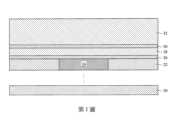
第1圖和方法200的操作202繪示了在半導體基板20上方形成介電層。第1圖繪示第一介電層22在半導體基板20上方。半導體基板20可能是或包括體半導體(bulk semiconductor)、絕緣體上矽(semiconductor-on-insulator,SOI)基板、或類似的基板,基板可能是摻雜的(例如,以p型或n型摻雜劑摻雜)或未摻雜的。在一些實施方式中,半導體基板20的半導體材料可能包括像矽(Si)和鍺(Ge)的元素半導體;化合物半導體;合金半導體;或其組合。FIG. 1 and
各個不同的裝置可能在半導體基板20之上。例如,半導體基板20可能包括場效電晶體(FETs),諸如鰭式場效電晶體(FinFETs)、平面場效電晶體、垂直閘極全環電晶體(VGAA FETs),或類似的電晶體;二極體;電容;和其他裝置。裝置可能例如:完全地形成在半導體基板20之內,形成在半導體基板20的一部分之內和在一或多個上覆層的一部分之內,和/或完全地形成在一或多個上覆層之內。本文描述的製程可能用於形成裝置和/或將裝置互相連接,以形成積體電路。積體電路可以是任何電路,諸如用於特定用途積體電路(Application Specific Integrated Circuit,ASIC)、處理器、記憶體、或其他電路。Various devices may be on the
第一介電層22高於半導體基板20。第一介電層22可能直接在半導體基板20之上,或是可能在介於第一介電層22和半導體基板20之間設置任何數目的其他層。例如,第一介電層22可能是或包括金屬間介電質(Inter-Metal Dielectric,IMD)或層間介電質(Inter-Layer Dielectric,ILD)。例如,第一介電層22可能是或包含低介電常數介電質,其具有小於約4.0的介電常數值(k-value),諸如約2.0或更小。在一些實施例中,第一介電層22包含矽氧化物、磷矽酸鹽玻璃(PSG)、硼磷矽酸鹽玻璃(BPSG)、氟矽酸鹽玻璃(FSG)、SiOxCy、矽碳材料、其化合物,其複合物、或其組合。The
導電特徵24在第一介電層22之內和/或穿過第一介電層22。導電特徵24可能是或包括導電線和/或導電導孔、電晶體的閘極結構、或接觸插塞(其連至電晶體的閘極結構和/或連至電晶體的源極/汲極區域)。在一些實施例中,第一介電層22為金屬間介電質,且導電特徵24可能包括導電線和/或導電導孔(共同或個別「互連結構」)。形成互連結構可能經由穿過金屬間介電質和/或在金屬間介電質內形成開口和/或凹陷,例如:使用鑲嵌製程。以下進一步描述形成互連結構的一些實施例,儘管可能實施其他製程和互連結構。在其他實施例中,第一介電層22可能包括層間介電質,且導電特徵24可能包括例如使用閘極置換製程在層間介電質內形成的閘極電極(例如:鎢、鈷等)。在另一個的實施例中,第一介電層22可能是層間介電質,且導電特徵24可能包括接觸插塞。形成接觸插塞可能經由形成穿過層間介電質的開口至例如在半導體基板20之上形成的電晶體的閘極電極和/或源極/汲極區域。接觸插塞可以包括黏著層(例如:鈦等)、在黏著層之上的阻障層(例如:氮化鈦(TiN)等)、和在阻障層之上的導電填充材料(例如:鎢、鈷等)。接觸插塞也可以由較少擴散性的金屬如鎢、鉬或釕來製造,而沒有阻障層。Conductive features 24 are within and/or through first
第一蝕刻停止層(ESL)26在第一介電層22和導電特徵24上方。一般而言,在形成例如接觸或導電導孔時,蝕刻停止層可以提供終止蝕刻製程的機制。蝕刻停止層可能由介電材料形成,此介電材料具有與相鄰的層或組件不同的蝕刻選擇性。第一蝕刻停止層26沉積在第一介電層22和導電特徵24二者的頂表面之上。第一蝕刻停止層26可能包含或者是矽氮化物、矽碳氮化物、矽碳氧化物、碳氮化物等,或其組合,而且可能經由化學氣相沉積(CVD)、電漿輔助化學氣相沉積(PECVD)、原子層沉積(ALD)、或其他沉積技術而沉積。在一些實施例中,第一蝕刻停止層26的厚度在從約3奈米至約10奈米的範圍內。A first etch stop layer (ESL) 26 is over the
第二介電層28在第一蝕刻停止層26上方。例如,第二介電層28可能是或包括金屬間介電質。第二介電層28沉積在第一蝕刻停止層26的頂表面之上。例如:第二介電層28可能是或包含低介電常數介電質,其具有小於約4的介電常數值,諸如約2或更小。在一些實施例中,第二介電層28包含矽氧化物、磷矽酸鹽玻璃、硼磷矽酸鹽玻璃、氟矽酸鹽玻璃、SiOxCy、矽碳材料、其化合物,其複合物、或其組合。沉積第二介電層28可能利用化學氣相沉積,諸如電漿輔助化學氣相沉積、或流動式化學氣相沉積(FCVD);旋轉塗佈;或其他沉積技術。在一些實施例中,可能執行化學機械平坦化(CMP)或其他平坦化製程,以將第二介電層28的頂表面平坦化。在一些實施例中,第二介電層28的厚度在從約4奈米至約30奈米的範圍內。The
第二蝕刻停止層30在第二介電層28上方。第二蝕刻停止層30沉積在第二介電層28的頂表面之上。第二蝕刻停止層30可能包含或者是矽氮化物、矽碳氮化物、矽碳氧化物、碳氮化物等,或其組合,並且可能經由化學氣相沉積、電漿輔助化助氣相沉積、原子層沉積、或其他沉積技術而沉積。在一些實施例中,第二蝕刻停止層30的厚度在從約3奈米至約10奈米的範圍內。A second
第三介電層32在第二蝕刻停止層30上方。例如,第三介電層32可能是或者包括金屬間介電質。第三介電層32沉積在第二蝕刻停止層30的頂表面之上。第三介電層32,例如可能是或者包含低介電常數介電質,其具有小於約4的介電常數值,諸如約2.0或更小。在一些實施例中,第三介電層32包含矽氧化物、磷矽酸鹽玻璃、硼磷矽酸鹽玻璃、氟矽酸鹽玻璃、SiOxCy、矽碳材料、其化合物,其複合物、或其組合。沉積第三介電層32可能使用化學氣相沉積,諸如電漿輔助化學氣相沉積、或流動式化學氣相沉積;旋轉塗佈;或其他沉積技術。在一些實施例中,可能執行化學機械平坦化或其他平坦化製程,以將第三介電層32的頂表面平坦化。在一些實施例中,第三介電層32的厚度在從約20奈米至約50奈米的範圍內,諸如約45奈米。The
第1圖的第二介電層28、第二蝕刻停止層30、和第三介電層32的配置是一個實施例。在其他實施例中,介於第二介電層28和第三介電層32之間的第二蝕刻停止層30可能省略。此外,在一些實施例中,可能在第二介電層28、第二蝕刻停止層30、和第三介電層32的位置形成單個介電層。本領域的普通技術技術人員會很容易地理解這些和其他可能進行的修改。The configuration of the
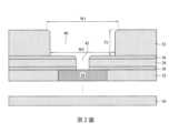
第2圖和方法200的操作204繪示導孔開口42和溝槽40形成在和/或穿過第一蝕刻停止層26、第二介電層28、第二蝕刻停止層30、和第三介電層32。形成導孔開口42和溝槽40可以使用光學微影和蝕刻製程,諸如使用於雙鑲嵌製程中。例如,光阻可以形成在第三介電層32之上,諸如經由使用旋轉塗佈,並且經由使用適當的光罩將光阻曝光,利用與溝槽40相對應的圖案進行圖案化。然後,根據使用的是正光阻或負光阻,可能移除光阻的曝光或未曝光的部分。光阻的圖案之後可能轉移到第三介電層32,諸如經由合適的蝕刻製程,其在第三介電層32內形成溝槽40。蝕刻製程可能包括反應性離子蝕刻(RIE)、中性粒子束蝕刻(NBE)、感應耦合電漿(ICP)蝕刻等,或其組合。蝕刻製程可能是各向異性的。第二蝕刻停止層30可能用來作為蝕刻製程的蝕刻終止。隨後,在例如灰化或濕式剝離製程中移除光阻。之後,可以在第三介電層32之上和在溝槽40之內形成另一個光阻,諸如經由旋轉塗佈,並且經由使用合適的光罩將光阻曝光,利用與導孔開口42相對應的圖案進行圖案化。光阻的圖案之後可能通過第二蝕刻停止層30、第二介電層28、和第一蝕刻停止層26而轉移,諸如經由一或多個合適的蝕刻製程,蝕刻製程形成導孔開口42,開口42穿過第二蝕刻停止層30、第二介電層28、和第一蝕刻停止層26。蝕刻製程可能包括反應性離子蝕刻、中性粒子束蝕刻、感應耦合電漿蝕刻等、或其組合。蝕刻製程可能是各向異性的。隨後,在例如灰化或濕式剝離製程中移除光阻。FIG. 2 and
溝槽40的側壁和導孔開口42的側壁被繪示為基本上垂直的和在拐角處為圓狀的。例如,側壁的線狀部分形成一角度,其是由內測量相應的第二介電層28或第三介電層32的角度,此角度在從約85度至約90度的範圍內,諸如約85度至約89度,更特定為約87度。在其他實施例中,溝槽40和導孔開口42的其一或二者的側壁可能是垂直的,或者可能在朝向或遠離導孔開口42的底部的方向漸縮。例如,導孔開口42可能具有正錐形輪廓(positive taper profile)或凹角型輪廓(reentrant profile)。關於導孔開口42的配置的各種實施例及其細節在第13圖至第18圖中繪示和描述。The sidewalls of
在第2圖的示例性配置中,溝槽40具有在第三介電層32的頂表面的平面的第一寬度W1,並且溝槽40具有沿著溝槽40的底表面的第二寬度W2。在一些實施例中,第一寬度W1在從約20奈米至約40奈米的範圍內,並且在一些實施例中,第二寬度W2在從約18奈米至約36奈米的範圍內。溝槽具有深度,在本實施例中,溝槽的深度等於第三介電層32的第一厚度T1。在一些實施例中,如前所述,第一厚度T1在從約20奈米至約50奈米的範圍內。第一厚度T1相對於第一寬度W1的第一縱橫比(aspect ratio)可以在從約0.5至約2.5的範圍內,並且第一厚度T1相對於第二寬度W2的第二縱橫比可以在從約0.56至約2.78的範圍內。In the exemplary configuration of FIG. 2,
在溝槽的側壁是垂直的示例性配置中,對應於第2圖中的第一寬度W1和第二寬度W2的寬度是相等的,並且每一個寬度可以在從約20奈米至約40奈米的範圍內。在此實施例中,第一厚度T1相對於溝槽40的寬度的縱橫比可以在從約0.5至約2.5的範圍內。在溝槽的側壁是漸縮的示例性配置中(例如:正錐形輪廓),對應於第2圖中的第一寬度W1的寬度,可能是對應於第2圖中的第二寬度W2的寬度(Wlower)和第三介電層32由內所測量的側壁的角度(θ)的函數(例如:Wupper=Wlower+[2T1(tanθ)-1])。對應於第2圖中的第二寬度W2的寬度可以在從約18奈米至約36奈米的範圍內,並且角度可以在從約85度至約89度的範圍內,或是可能小於85度。第一厚度T1相對於對應於第2圖的第二寬度W2的寬度的縱橫比可以在從約0.56至約2.78的範圍內。In an exemplary configuration in which the sidewalls of the trenches are vertical, the widths corresponding to the first width W1 and the second width W2 in FIG. within the range of meters. In this embodiment, the aspect ratio of the first thickness T1 relative to the width of the
本領域普通技術人員會容易地理解這裡所描述的尺寸、比率、和角度僅僅是實施例。尺寸、比率、和角度可以基於技術世代節點其中實施的各個方面而變化,和/或基於所使用的各種製程而變化。這樣的變化在本揭示內容的範圍之內。Those of ordinary skill in the art will readily understand that the dimensions, ratios, and angles described herein are examples only. Dimensions, ratios, and angles may vary based on various aspects implemented therein by technology generation node, and/or based on various processes used. Such variations are within the scope of this disclosure.
第3圖和方法200的操作206繪示形成襯層50,襯層50共形地沿著導孔開口42和溝槽40二者的側壁、沿著導孔開口42和溝槽40的各自的底表面、以及沿著第三介電層32的頂表面。襯層50可以經由共形的沉積而形成。襯層50可能是或者包含矽氮化物(SiN)、碳氧化矽(SiOC)、矽碳氮化物(SiCN)、矽氧碳氮化物(SiOCN)、含矽低介電常數介電質、含碳低介電常數介電質等,或其組合,而且可能經由化學氣相沉積、原子層沉積、或其他沉積技術而沉積。在一些實施例中,襯層50的厚度在從約1奈米至約4奈米的範圍內,更特定為從約2奈米至約3奈米。
第4圖和方法200的操作208繪示從襯層50形成各個襯裡52,各個襯裡52沿著導孔開口42的側壁和沿著溝槽40的側壁。襯裡52可以經由各向異性地蝕刻襯層50而形成。各向異性蝕刻襯層50的蝕刻製程可能包括反應性離子蝕刻、中性粒子束蝕刻、感應耦合電漿蝕刻等,或其組合。襯裡52和第二蝕刻停止層30,如果有實施的話,可能是擴散阻障,其可以減少或預防隨後沉積在溝槽40內和導孔開口42內的導電填充材料的向外擴散,例如擴散至第二介電層28和第三介電層32。襯裡52和第二蝕刻停止層30可以形成介電的擴散阻障。FIG. 4 and
除其他外,襯裡52的輪廓可以根據溝槽40和導孔開口42二者的側壁的輪廓而變化。在第4圖的實施例中,在拐角的斜率為大約45°的側壁上的圓角處,第二厚度T2可以基本上等於襯層50的第一厚度TL減去通過異向性蝕刻在垂直方向上去除的厚度(tetched)的乘上2的除以2的平方根(例如:TL-[tetched x 2-(1/2)])。此外,第三厚度T3其沿著溝槽40的底部或導孔開口42的底部的各側壁的基本上垂直的部分,可以等於襯層50的第一厚度TL。在一些實施例中,第二厚度T2在從約0.3奈米至約1.2奈米的範圍內,且第三厚度在從約1奈米至約4奈米的範圍內。本領域普通技術人員將很容易理解襯裡52的厚度與側壁的下斜角度之間可以具有關聯性。The profile of
在溝槽的側壁為垂直的例性的配置中,對應於第4圖中的第二厚度T2的厚度,相同於對應於第4圖中的第三厚度T3的厚度(其可以進一步基本上等於襯層50的第一厚度TL),而且每個厚度可以在從約1奈米至約4奈米的範圍內。在溝槽的側壁為漸縮性的配置中(例如:正錐形輪廓),在一樣的傾斜角度處,對應於第4圖中的第二厚度T2的厚度,相同於對應於第4圖中的第三厚度T3的厚度。類似於上文所述的本領域普通技術人員所理解的,厚度可以是襯層50的第一厚度TL和側壁的角度的函數。與第2圖中的第二寬度W2相對應的寬度可以在從約1奈米至約4奈米的範圍內。In an exemplary configuration in which the sidewalls of the trench are vertical, the thickness corresponding to the second thickness T2 in FIG. 4 is the same as the thickness corresponding to the third thickness T3 in FIG. 4 (which may further be substantially equal to The first thicknessTL of the liner 50 ), and each thickness may be in a range from about 1 nm to about 4 nm. In configurations in which the sidewalls of the trench are tapered (for example: forward tapered profile), at the same angle of inclination, the thickness corresponding to the second thickness T2 in Figure 4 is the same as that corresponding to the second thickness T2 in Figure 4 The thickness of the third thickness T3. The thickness may be a function of the first thicknessTL of the
襯裡52的輪廓可以根據用於沉積襯層50的沉積製程的階梯覆蓋而進一步變化。例如,由於階梯覆蓋變化,沿著導孔開口42的側壁的襯裡52的厚度可以不同於沿著溝槽40的側壁的襯裡52的厚度。The profile of
在方法200的操作210中,在形成襯裡52之後,選擇性地,可能執行清潔製程,以清潔例如溝槽40和導孔開口42的暴露的表面。清潔製程可以包括電漿處理、蝕刻製程、其他清潔製程、或其組合。在一實施例中,清潔製程包括電漿處理(操作212),接著是原子層蝕刻(ALE)(操作214)。操作212中的電漿處理可以包括使用氫氣(H2)與例如氬氣(Ar)的載體氣體。在某些情況下,電漿處理可以減少氧化物,氧化物可能形成在穿過導孔開口42暴露的導電特徵24的表面上,且電漿處理可以移除在各個表面上可能形成的有機材料。電漿處理中的氫氣流速可以在從約5sccm至約1,000sccm的範圍內,並且電漿處理中的載體氣體的流速可以在從約0sccm至約1,000sccm的範圍內。電漿處理的壓力可以在從約10毫托(mTorr)至約200毫托的範圍內。電漿處理的溫度可以在從約-20℃至約100℃的範圍內。電漿處理的電漿發生器的功率可以在從約20W至約400W的範圍內,並且電漿發生器的頻率可以是約13.56MHz或更高。電漿處理期間的基板可以加偏壓(be biased),在從約20V至約100V的範圍內。電漿處理的持續時間可以在從約5秒至約120秒的範圍內。In
操作214中的原子層蝕刻在第12圖中進一步詳細繪示。操作214中的原子層蝕刻可以包括執行多個循環,諸如在從2個循環至25個循環的範圍內。原子層蝕刻的一個循環可以包括依序地將反應氣體,諸如三氯化硼(BCl3)氣體,與載體氣體(例如氬氣(Ar))一起流動(操作250);吹除(purging)(操作252)反應氣體;將蝕刻劑氣體(諸如氫氣(H2))與載體氣體(例如氬氣(Ar))一起流動(操作254),並且可能加上電漿輔助(plasma enhancement);以及吹除(操作256)蝕刻劑氣體。在一些實施例中,反應氣體,例如:三氯化硼(BCl3)氣體,被吸附在介電質表面上以形成單層,且沒有顯著地被吸附在金屬表面上,並且經由蝕刻劑氣體(例如:氫氣(H2))的流動來蝕刻單層。在此提供的實施例實施了以三氯化硼(BCl3)氣體作為反應氣體,和以氫氣(H2)作為蝕刻劑氣體;也可能使用其他氣體。在三氯化硼(BCl3)氣體的流動期間,三氯化硼(BCl3)氣體的流速可以在從約20sccm至約180sccm的範圍內,並且載體氣體的流速可以在從約200sccm至約800sccm的範圍內。此外,在三氯化硼(BCl3)氣體的流動期間,原子層蝕刻的壓力可以在從約15毫托至約100毫托的範圍內,並且原子層蝕刻的溫度可以在從約-20℃至約60℃的範圍內。在三氯化硼被吹除之後,氫氣(H2)開始流動並且點燃電漿。在氫氣(H2)的流動期間,氫氣(H2)的流速可以在從約5sccm至約1,000sccm的範圍內,且載體氣體的流速可以在從約50sccm至約400sccm的範圍內。此外,在氫氣(H2)的流動期間,原子層蝕刻的壓力可以在從約10毫托至約200毫托的範圍內,並且原子層蝕刻的溫度可以在從約-20℃至約20℃的範圍內。原子層蝕刻的電漿發生器的功率可以在從約10W至約800W的範圍內,並且電漿發生器的頻率可以是約13.56MHz或更高。在原子層沉積的電漿處理期間,基板可以加偏壓,在從約50V至約300V的範圍內。The atomic layer etch in
以上描述的製程是清潔製程(操作210)的一個實施例(操作210)。在一些實施方式中(以下參考第19圖至第22圖進一步描述),清潔製程包括電漿製程,接著是鹵化物浸泡,接著是還原處理。The process described above is one embodiment (operation 210) of the cleaning process (operation 210). In some embodiments (further described below with reference to FIGS. 19-22 ), the cleaning process includes a plasma process followed by a halide soak followed by a reduction treatment.
在方法200的操作216中,在可選地執行操作210中的清潔製程之後,可以可選地在暴露的介電質表面(例如:溝槽40和導孔開口42的暴露的介電質表面)上執行選擇性輔助處理。選擇性輔助處理可以例如處理和/或鈍化介電質表面,比起沒有經過這樣處理的介電質表面,隨後的金屬的沉積具有更高的選擇性,以在金屬表面上用較快的速率沉積金屬。例如,選擇性輔助處理可以使介電質表面成為疏水性的,這可以改善隨後的金屬的沉積期間的選擇性。選擇性輔助處理可以包括使含矽的烴氣體流過介電質表面。選擇性輔助處理可以是三甲基矽氧烷(TMS)處理、二甲基矽氧烷(DMS)處理等、或其組合。示例性含矽的烴氣體包括1,1,1,3,3,3-六甲基二矽氮烷(1,1,1,3,3,3-hexamethyldisilazane,HDMS)、三甲基氯矽烷(chlorotrimethylsilane,TMCS)、N,O-雙(三甲基甲矽烷基)乙酰胺(N,O-bis(trimethylsilyl)acetamide,BSA),N-(三甲基甲矽烷基)二甲胺(N-(trimethylsilyl)dimethylamine,TMS-DMA)、TMS-咪唑(SIM,N-三甲基矽咪唑(N-trimethylsilylimidazole))、1,1,3,3-四甲基二矽氮烷(1,1,3,3-tetramethyldisilazane,TMDS)、氯二甲基矽烷(chlorodimethylsilane,DMCS)等、或其組合。選擇性輔助處理可以導致矽烷化過程,其中在介電質表面終端處的原子或原子團可以被含矽的烴的物質種類取代,這可以導致介電質表面呈現疏水性。含矽的烴的流速可以在從約5sccm至約100sccm的範圍內,並且與含矽的烴流動的載體氣體的流速可以在從約0sccm至約400sccm的範圍內。在含矽的烴的流動期間的壓力可以在從約1毫托至約100毫托的範圍內,並且溫度可以在從約20℃至約300℃的範圍內。選擇性輔助處理可以處理或鈍化襯裡52、第二蝕刻停止層30、和第三介電層32這些層的暴露的介電質表面,以改善在導電特徵24上隨後的選擇性沉積的選擇性。In
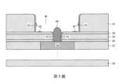
第5圖和方法200的操作218繪示在導孔開口42內形成導電導孔60。導電導孔60的形成可以包括選擇性沉積。例如,選擇性沉積可以使用穿過導孔開口42所暴露的導電特徵24作為晶種。選擇性沉積可以包括無電沉積或鍍、選擇性化學氣相沉積、或其他技術。導電導孔60可以是或者包括金屬,例如鈷(Co)、釕(Ru)等、或其組合。在一實施例中,導電導孔60是鈷,使用無電沉積或鍍將鈷沉積。鈷(Co)的無電沉積或鍍可能處於等於或小於約200℃的範圍內的溫度,例如在從室溫(例如,約23℃)至約200℃的範圍內。選擇性化學氣相沉積可以包括使用前趨物氣體,包含Ru3(CO)12、C10H10Ru、C7H9RuC7H9、Ru(C5(CH3)5)2等、或其組合,以及載體氣體,諸如氬(Ar)。前趨物氣體的流速可以在從約5sccm至約100sccm的範圍內,並且載體氣體的流速可以在從約10sccm至約400sccm的範圍內。選擇性化學氣相沉積的壓力可以在從約0.2毫托至約20毫托的範圍內。選擇性化學氣相沉積的溫度可以小於或等於約200℃,例如在從室溫(例如約23℃)至約200℃的範圍內。FIG. 5 and
如第5圖所示,導電導孔60的上表面是凸形的。在其他實施例中,導電導孔60的上表面可以是凹形的或平面的。在導孔開口42內所形成的用於導電導孔60的配置的各種實施例、以及其細節在第13圖至第18圖繪示和描述。As shown in FIG. 5, the upper surface of the conductive via 60 is convex. In other embodiments, the upper surface of the conductive via 60 may be concave or planar. Various embodiments of configurations for
如第5圖所示,在用於形成導電導孔60的選擇性沉積期間,可能形成一些殘留的沉積位點62。殘留的沉積位點62可能形成在各個表面上,諸如在溝槽40內的第二蝕刻停止層30的表面和襯裡52的表面。As shown in FIG. 5, during the selective deposition used to form the
第6圖和方法200的操作220繪示了選擇性回蝕刻的執行,選擇性回蝕刻移除了殘留的沉積位點62。回蝕刻可以是乾式(例如:電漿)蝕刻製程、濕式蝕刻製程、或是其組合。電漿蝕刻可以包括使用氟碳(CxFy)氣體、氯氟碳(CxClyFz)氣體、氯化碳(CxCly)氣體等、或其組合。濕式蝕刻可以包括使用一種或多種如下的溶液:標準清潔-1(SC1)、標準清潔-2(SC2)、硫酸-過氧化氫混合物(SPM)、稀釋氫氟酸(dHF)、過氧化氫(H2O2)、緩衝氧化物蝕刻(BOE)溶液、鹽酸(HCl)酸等、或其組合。溶液的溫度可以在從約20℃至約90℃的範圍內,基板在溶液中的浸置的持續時間可以在從約10秒至約120秒的範圍內。FIG. 6 and
第7圖和方法200的操作222繪示了成核輔助處理的執行,成核輔助處理沿著例如包括導電導孔60的上表面的溝槽40內的暴露的表面,以形成處理過的表面70。一般而言,成核輔助處理使沿著例如溝槽40內的暴露的表面的鍵斷裂,以增强後續沉積製程中材料的吸附能力。在一些實施例中,成核輔助處理包括濺射(操作224)、離子佈植(操作226)、電漿處理(操作228)、紫外線(UV)處理(操作230)、電漿摻雜(操作232)等、或其組合。成核輔助處理可以是方向性的(例如:各向異性的),或共形的(例如:等向性的)。在一些實施例中,成核輔助處理可以處理例如垂直的表面,儘管在處理的程度上小於例如水平的表面。成核輔助處理的執行程度(例如:沿著表面鍵被斷裂的程度)可以影響許多成核位點,並且因此至少影響稍後沉積的導電填充材料80的初始沉積速率,這將在隨後描述。一般而言,被斷裂的鍵越多,產生的懸鍵越多,因此,至少在沉積剛開始時,可能有越多的成核位點可用於導電填充材料80的吸附和成核作用,以增加沉積速率。在一些實施例中,成核輔助處理可以是方向性的,以基本上僅處理水平的表面(例如:經由溝槽40暴露的第二蝕刻停止層30的頂表面和導電導孔60的上表面),這可以使得在溝槽40內導電填充材料自底部向上沉積,並且減少在溝槽40內的導電填充材料內形成的接縫和空洞。FIG. 7 and
在一實施例中,成核輔助處理是使用氬(Ar)氣的濺射(操作224)。氬氣的流速可以在從約10sccm至約2,000sccm的範圍內。濺射的壓力可以在從約0.5毫托至約50毫托的範圍內,且濺射溫度可以在從約-20℃至約120℃的範圍內。濺射的電漿發生器的功率可以在從約100W至大約2,000W的範圍內,並且電漿發生器的頻率可以是約13.56MHz或更高。在濺射期間,基板可以加偏壓,在從約50V至約300V的範圍內。雖然在一些實施例中,濺射可以是共形的,但是濺射可以是方向性的(例如:處理水平的表面)。濺射可以使氬被沉積在處理過的表面70上和/或嵌入至處理過的表面70的下方的深度中相應的材料內。例如,可以將用於濺射的物質種類(例如,氬)嵌入到形成處理過的表面70(例如:導電導孔60、第二蝕刻停止層30、溝槽40內的襯裡52、和第三介電層32)的材料內,嵌入至一深度處的相應的材料內,此深度為從處理過的表面70的等於或小於約2奈米的深度,並且濃度在從約1×1018cm-3至約1×1019cm-3的範圍內。物質種類的濃度可以從靠近相應的處理過的表面70的峰值降低到材料中的一深度處。濺射可以經由物質種類與暴露的(例如,處理過的表面70)材料的原子碰撞來破壞鍵。In one embodiment, the nucleation assisting process is sputtering using argon (Ar) gas (operation 224 ). The flow rate of argon may range from about 10 seem to about 2,000 seem. The sputtering pressure may range from about 0.5 mTorr to about 50 mTorr, and the sputtering temperature may range from about -20°C to about 120°C. The power of the plasma generator for sputtering can range from about 100 W to about 2,000 W, and the frequency of the plasma generator can be about 13.56 MHz or higher. During sputtering, the substrate may be biased in a range from about 50V to about 300V. The sputtering can be directional (eg, to treat a horizontal surface), although in some embodiments the sputtering can be conformal. Sputtering may cause argon to be deposited on the treated
在另一個實施例中,成核輔助處理是束線式離子佈植(beam line implantation)(操作226)。用於束線式離子佈植的物質種類可以包括矽(Si)、鍺(Ge)、碳(C)、氮(N)、氬(Ar)等、或其組合。佈植能量可以在從約2keV至約10keV的範圍內。佈植的劑量可以在從約1013cm-2至約2x1015cm-2的範圍內。佈植可以至一深度,其是相應的暴露的表面的從約1奈米至約4奈米範圍內的深度,並且佈值至植入的物質種類的濃度在從約5x1018cm-3至約5x1021cm-3的範圍內。物質種類的濃度可以從靠近相應的處理過的表面70的峰值降低到材料中的一深度處。束線式離子佈植可以是方向性的,雖然在一些實施例中,可能執行多重佈植,以達到更為共形的處理。束線式離子佈植可以經由植入的物質種類與被植入的材料(例如,處理過的表面70)的原子碰撞,而使鍵斷裂。In another embodiment, the nucleation-assisted treatment is beam line implantation (operation 226). The species used for beamline ion implantation may include silicon (Si), germanium (Ge), carbon (C), nitrogen (N), argon (Ar), etc., or combinations thereof. The implant energy can range from about 2 keV to about 10 keV. The dose for implantation may range from about 1013 cm−2 to about 2×1015 cm−2 . The implantation may be to a depth that is a depth ranging from about 1 nanometer to about 4 nanometers of the corresponding exposed surface, and the concentration of the implanted species is from about 5×1018 cm−3 to within the range of about 5x1021 cm-3 . The concentration of species may decrease from a peak near the corresponding treated
在更進一步的實施例中,成核輔助處理為電漿處理(操作228)。電漿處理可以包括使用氣體,氣體包含氙(Xe)、氬氣(Ar)、氫(H2)、氮(N2)等、或其組合。氣體的流速可以在從約10sccm至約2,000sccm的範圍內。電漿處理的壓力可以在從約10毫托至約100毫托的範圍內,並且電漿處理的溫度可以在從約-20℃至約60℃的範圍內。電漿處理的電漿發生器的功率可以在從約20W至約200W的範圍內,並且電漿發生器的頻率可以是約13.56MHz或更高。在電漿處理期間,基板可以加偏壓,在從約50V至約300V的範圍內。電漿的物質種類可以破壞暴露的表面並且可以擴散進暴露的表面之內。電漿處理可以是共形的或是方向性的。電漿處理可以導致電漿的物質種類嵌入在處理過的表面70上和/或擴散至處理過的表面70下方的一深度處的相應的材料內。例如,用於電漿的物質種類(例如:氙、氬、氫等)可以擴散進形成處理過的表面70(例如:導電導孔60、第二蝕刻停止層30、溝槽40內的襯裡52、以及第三介電層32)的材料內,至一深度處的相應的材料內,此深度為從處理過的表面70的等於或小於約5奈米的深度,並在物質種類的濃度從約1x1018cm-3至1x1020cm-3的範圍內。物質種類的濃度可以從靠近相應的處理過的表面70的峰值降低到材料中的一深度處。In still further embodiments, the nucleation assisting treatment is plasma treatment (operation 228). Plasma treatment may include using a gas including xenon (Xe), argon (Ar), hydrogen (H2 ), nitrogen (N2 ), etc., or combinations thereof. The flow rate of the gas may range from about 10 seem to about 2,000 seem. The pressure of the plasma treatment may range from about 10 mTorr to about 100 mTorr, and the temperature of the plasma treatment may range from about -20°C to about 60°C. The power of the plasma generator for plasma treatment may range from about 20 W to about 200 W, and the frequency of the plasma generator may be about 13.56 MHz or higher. During plasma processing, the substrate may be biased in a range from about 50V to about 300V. Plasma species can damage exposed surfaces and can diffuse into exposed surfaces. Plasma treatments can be conformal or directional. Plasma treatment may cause plasma species to become embedded on and/or diffuse into corresponding materials at a depth below treated
在又進一步的實施例中,成核輔助處理為紫外光(UV)處理(操作230)。紫外光處理可以包括將基板暴露於所在環境中的紫外光。所在環境可以包括氣體,氣體包含氬(Ar)、氖(Ne)、氙(Xe)等、或其組合。紫外光暴露的能量可以在從約3.4eV至約10eV的範圍內。紫外光暴露的持續時間可以等於或小於約300秒,諸如在從約15秒至約300秒的範圍內。紫外光處理可以使暴露的表面上的鍵斷裂,從而破壞暴露的表面。紫外光處理過程中,所在環境的物質種類可以擴散進暴露的表面內。例如,所在環境的物質種類(例如:氙、氬、氖等)可以擴散進所形成的處理過的表面70(例如:導電導孔60、第二蝕刻停止層30、溝槽40內的襯裡52、以及第三介電層32)的材料內,至一深度處的相應的材料內,此深度為從處理過的表面70的等於或小於約5奈米的深度。物質種類的濃度可以從靠近相應的處理過的表面70的峰值降低到材料內的一深度處。紫外光處理可以是方向性的,雖然在一些實施例中,可能執行多重的紫外光處理以實現更為共形的處理。In yet a further embodiment, the nucleation assisting treatment is an ultraviolet (UV) treatment (operation 230). UV light treatment may include exposing the substrate to UV light in the environment. The environment can include gases, including argon(Ar), neon (Ne), xenon (Xe), etc., or a combination thereof. The energy of the ultraviolet light exposure can range from about 3.4 eV to about 10 eV. The duration of the ultraviolet light exposure may be equal to or less than about 300 seconds, such as in a range from about 15 seconds to about 300 seconds. Ultraviolet light treatment can damage the exposed surface by breaking bonds on the exposed surface. Species from the environment can diffuse into exposed surfaces during UV light treatment. For example, ambient species (e.g., xenon, argon, neon, etc.) can diffuse into the formed treated surface 70 (e.g., conductive via 60, second
在又進一步的實施例中,成核輔助處理為電漿摻雜(操作232)。用於電漿摻雜所實施的物質種類可以包括硼(B)、氬(Ar)等、或其組合。摻雜可以至相應的暴露的表面的一深度處,其在從約1奈米至約5奈米範圍內,摻雜至物質種類的濃度在從約1×1019cm-3至約1×1020cm-3的範圍內。物質種類的濃度可以從靠近相應的處理過的表面70的峰值降低到材料中的一深度處。電漿摻雜可以經由植入的物質種類與被植入的材料的原子(例如,處理過的表面70)碰撞而破壞鍵。In yet a further embodiment, the nucleation assisting treatment is plasma doping (operation 232). Species performed for plasma doping may include boron (B), argon (Ar), etc., or combinations thereof. The doping may be to a depth corresponding to the exposed surface in the range of from about 1 nm to about 5 nm, to a concentration of species of from about 1×1019 cm−3 to about 1× 1020 cm-3 range. The concentration of species may decrease from a peak near the corresponding treated
第8圖和方法200的操作234繪示了在處理過的表面70之上形成導電填充材料80,例如:填充溝槽40。導電填充材料80的形成可能經由沉積製程,其在介電質表面上以及金屬的表面上沉積導電填充材料80。參照第7圖所描述的成核輔助處理,在介電質表面(例如:在處理過的表面70上)上可以製造成核位點,在沉積期間,導電填充材料80可以被吸附至成核位點上。因此,諸如取決於成核輔助處理的方向性,導電填充材料80的沉積可以是自底向上的沉積和/或共形的沉積。在自底向上的沉積中,可以經由在溝槽40內垂直增長的導電填充材料80的單一生長前沿來避免接縫。Figure 8 and
由於共形的沉積的結果,接縫82可以在溝槽40內的導電填充材料80之內形成。接縫82可以由於在共形的沉積期間導電填充材料80的不同生長前沿的合併或聚結而產生。例如,源自沿著第三介電層32的側壁的襯裡52的側壁表面的生長前沿,可以與源自第二蝕刻停止層30的頂表面的生長前沿聚結或合併,以形成接縫82的至少一部分。接縫82可能各自包括,例如一或多個空洞、導電填充材料80的晶界、和/或生長前沿的聚結或合併的其他跡象。接縫82可以具有相對於垂直方向(例如:垂直於第二蝕刻停止層30的頂表面)的角度86。角度86可以在從約25°至約75°的範圍內,並且更特定為從約30°至約60°的範圍內。角度86可以受到襯裡52的側壁表面相對於導電導孔60的接近度的影響。在一些實施例中,導電填充材料80在從導電導孔60處的成長速率比從介電質表面(諸如襯裡52的側壁)處的成長速率快,例如快約2倍至約3倍。因此,在這樣的實施例中,襯裡52的側壁越靠近導電導孔60,角度86可能越小。
在一些實施例中,導電填充材料的沉積包括使用化學氣相沉積、無電鍍或沉積、或其他沉積製程。導電填充材料80可以是或包括金屬,諸如:釕(Ru)、鎳(Ni)、鉬(Mo)、鈷(Co)、鎢(W)、銅(Cu)等、或其組合。在一些實施例中,導電填充材料80是或包括經由化學氣相沉積而沉積的釕(Ru)、鉬(Mo)、鈷(Co)、或鎢(W)。釕的示例性的前趨物包括十二羰基三钌(Ru3(CO)12)、CHORUS等、或其組合。鉬的示例性前趨物包括鉬(V)氯化物(MoCl5)、Mo(CO)5等,或其組合。鈷的示例性前趨物包括二鈷六羰基叔丁基乙炔(dicobalt hexacarbonyl tert-butylacetylene,CCTBA)等、或其組合。鎢的示例性前趨物包括六氟化鎢(WF6)、鎢(V)氯化物(WCl5)等,或其組合。在化學氣相沉積期間,前趨物氣體的流速可以在從約10sccm至約200sccm的範圍內,並且載體氣體(例如:氬(Ar))的流速可以在從約100sccm至約800sccm的範圍內。化學氣相沉積的壓力可以在從約0.2毫托至約20毫托的範圍內。化學氣相沉積的溫度可以小於或等於約175℃,諸如在從120℃至170℃的範圍內(特別是對於例如釕的沉積)。在其他實施例中,沉積鎳可以使用無電鍍或沉積。在沉積導電填充材料80之後,可能執行退火或回流(reflow)。In some embodiments, the deposition of the conductive fill material includes using chemical vapor deposition, electroless plating or deposition, or other deposition processes. The
在一些實施例中,可以分別地沿著包括矽和/或碳的介電材料的處理過的表面70,形成矽化物和/或碳化物。例如,假設襯裡52和第二蝕刻停止層30包括矽,成核輔助處理可以導致在處理過的表面70處的矽具有懸鍵,且導電填充材料80的金屬可以附著到懸鍵和/或與處理過的表面70的矽反應,以形成矽化物,其在介於導電填充材料80和襯裡52或第二蝕刻停止層30之間的介面處。在導電填充材料80的沉積期間(例如:當前趨物在處理過的表面70上流動時),和/或在導電填充材料80的沉積之後,導電填充材料80的金屬可以附著在懸鍵和/或與處理過的表面70的矽反應。類似地,例如,假設襯裡52和第二蝕刻停止層30包括碳,成核輔助處理可以導致在處理過的表面70處的碳具有懸鍵,且導電填充材料80的金屬可以附著到懸鍵和/或與處理過的表面70的碳反應,以形成碳化物(例如:金屬碳化物),其在介於導電填充材料80和襯裡52或第二蝕刻停止層30之間的介面處。在導電填充材料80的沉積期間(例如:當前趨物在處理過的表面70上流動時),和/或在導電填充材料80的沉積之後,導電填充材料80的金屬可以附著在懸鍵和/或與處理過的表面70的碳反應。利用處理過的表面70的矽和/或碳的懸鍵和/或斷裂的鍵,可以在處理過的表面70處形成矽化物和/或碳化物,以增進導電填充材料80的成核作用,並且促進導電填充材料80附著至介電層,諸如襯裡52和第二蝕刻停止層30。In some embodiments, silicides and/or carbides may be formed along the treated
在一些實施例中,在導電導孔60的處理過的表面70處,導電導孔60的金屬可能與導電填充材料80的金屬形成金屬合金或化合物。成核輔助處理可能破壞導電導孔60的處理過的表面70之處的鍵,以允許導電導孔60的金屬和導電填充材料80在導電導孔60的處理過的表面70處混合和/或反應。在導電填充材料80的沉積期間(例如:當前趨物在處理過的表面70上流動時),和/或導電填充材料80沉積之後,在處理過的表面70處,導電填充材料80的金屬可以與導電導孔60的金屬混合和/或反應。導電導孔60和導電填充材料80可能電性連接,而沒有明顯的電阻(由在成核輔助處理為了形成處理過的表面70而使用的物質種類所引起的電阻)。In some embodiments, the metal of the conductive via 60 may form a metal alloy or compound with the metal of the
更進一步地,在一些實施例中,在成核輔助處理中使用的物質種類可能例如通過吸附,擴散和/或佈植而嵌入處理過的表面70之內或之上,並且物質種類可能與導電填充材料80反應。例如,佈植進處理過的表面70之內的矽或鍺,可以與導電填充材料80的金屬反應,以形成金屬-半導體化合物(例如:分別為矽化物或鍺化物)。作為另一個實施例,佈植進處理過的表面70之內的碳,可以與導電填充材料80的金屬反應,以形成金屬碳化物,或者佈植進處理過的表面70之內的氮,可以與導電填充材料80的金屬反應,以形成金屬氮化物。在其他實施例中可以形成其他化合物。Further, in some embodiments, the species used in the nucleation-assisted treatment may be embedded in or on the treated
在一些實施例中,在成核輔助處理中使用的物質種類可能嵌入處理過的表面70之內或之上,並且可能保持與其他材料不發生反應。例如,惰性物質,諸如氬氣,可以在處理過的表面70處或附近保持不反應。未反應的物質種類可以擴散進各個介電層內。取決於成核輔助處理,未反應的物質種類的最高濃度可能在處理過的表面70(例如:介電層或導電導孔60的處理過的表面)處,並且從處理過的表面70往各個介電層或導電導孔60的方向減少,或是在從處理過的表面70往各個介電層或導電導孔60的方向上,可以在沿著此方向減少之前先增加至一峰值濃度,諸如在當物質種類經由束線式離子佈植、電漿摻雜、或類似的技術佈植時。In some embodiments, the species used in the nucleation assisting treatment may be embedded in or on the treated
在成核輔助處理中,使用的物質種類可能嵌入在不同的處理過的表面70之內或之上的程度,可能取決於成核輔助處理的方向性。例如,高度方向性的成核輔助處理,諸如束線式離子佈植,可以使得一些表面比其他表面具有更多的嵌入在內或在上的佈植的物質種類。具體的,在一些實施例中,水平的表面(例如:第二蝕刻停止層30的頂表面)可以具有比垂直表面(例如:襯裡52的側壁)更多的嵌入在內或在上的佈植的物質種類。在一些實施例中,可以在不同的方向執行多重的方向性成核輔助處理,以在不同的表面之間獲得更均勻的處理,諸如以不同的植入角度的多重束線式離子佈植。The extent to which species of species used in the nucleation-assisted treatment may be embedded in or on different treated
第9圖繪示移除多餘的導電填充材料80,以在第三介電層32內形成導電線84。使用平坦化製程,諸如化學機械平坦化,可以移除多餘的導電填充材料80和第三介電層32的處理過的表面70。第三介電層32可能進一步經由平坦化製程而薄化,在一些實施例中,平坦化製程可能移除溝槽40的圓角。在一些實施例中,第三介電層32薄化至厚度為從約10奈米至約30奈米的範圍內。移除多餘的導電填充材料80和第三介電層32的處理過的表面70,可以將導電填充材料80和第三介電層32二者的頂表面形成為共平面的。如前所述的接縫82可以保持在導電線84內。在一些實施例中,接縫82可能經由製程期間的退火或其他熱製程來固化(be cured)或移除。可以形成互連結構,諸如雙鑲嵌互連結構,如第9圖所示,互連結構包含導電導孔60和導電線84。FIG. 9 shows the removal of excess conductive filling
第10圖繪示了形成第三蝕刻停止層90和第四介電層92,二者在第三介電層32、導電線84和沿著溝槽40的側壁的襯裡52的上方,以及形成導電特徵94,其穿過第三蝕刻停止層90和第四介電層92而接觸導電線84。第三蝕刻停止層90可以沉積在第三介電層32、導電線84、和襯裡52之上。第三蝕刻停止層90可能包含或是為氮化矽、矽碳氮化物、矽碳氧化物、碳氮化物等,或其組合,並且可能經由化學氣相沉積、電漿輔助化學氣相沉積、原子層沉積、或其他沉積技術而沉積。第四介電層92沉積在第三蝕刻停止層90上方。例如,第四介電層92可能是或是包括金屬間介電質(IMD)。例如,第四介電層92可能是或是包含低介電常數介電質,其具有小於約4的介電常數,諸如約2或更小。在一些實施例中,第四介電層92包含矽氧化物、磷矽酸鹽玻璃、硼磷矽酸鹽玻璃、氟矽酸鹽玻璃、SiOxCy、矽碳材料、其化合物、其複合物、或其組合。沉積第四介電層92可能使用化學氣相沉積,諸如電漿輔助化學氣相沉積或流動式化學氣相沉積;旋轉塗佈;或其他沉積技術。在一些實施例中,可能執行化學機械平坦化或其他平坦化製程,以平坦化第四介電層92的頂表面。FIG. 10 illustrates the formation of a third
與導電線84接觸的導電特徵94可能是或包括例如導電導孔或其他導電特徵。導電特徵94可能使用鑲嵌製程而形成,諸如雙鑲嵌製程。例如,形成導電特徵94可能使用前述參照繪示於第2圖至第9圖所描述的製程,或使用類似的製程。
從前述內容顯見,在所描述的用於形成導電導孔60和導電線84的實施例中,不沉積晶種層和含金屬的阻障層。在圖示和描述的實施例中,沒有沉積晶種層和含金屬的阻障層於(i)在介於導電線84和任何在其上或在其內沉積的介電層(例如:第三介電層32或第二蝕刻停止層30)之間,(ii)介於導電導孔60和任何在其內沉積的介電層之間(例如:第二蝕刻停止層30、第二介電層28、或第一蝕刻停止層26),或(iii)介於導電導孔60和導電線84之間一些實施方式可以實施晶種層和/或含金屬的阻障層。此外,雖然成核輔助處理的物質種類可能與導電線84(例如:導電填充材料80)和/或導電導孔60(諸如:導電導孔60的處理過的表面70(例如:在介於導電導孔60和導電線84之間的介面))的金屬反應,但是所產生的材料可能比沉積的阻障層更薄和/或具有更低的物質種類的濃度,並且,可能因此在一些情況下不是擴散阻障。例如,在一些實施成核輔助處理的實施例中,在導電線84中(例如:導電填充材料80)和/或在相應的處理過的表面處的導電導孔60,物質種類可以具有小於或等於約5原子的百分比(at.%)的濃度,諸如在從約0.1at.%至約5at.%的範圍內。因為其中的物質種類的濃度低,導電線84(例如:導電填充材料80)和/或導電導孔60內的物質種類的濃度可以是不連續的。此外,物質種類與導電線84和/或導電導孔60的導電材料可能不是在材料(例如金屬化合物)的相應的化合物的穩定相。As apparent from the foregoing, in the described embodiment for forming
第13圖至第18圖為根據一些實施方式,繪示了第6圖的中間結構的一部分截面圖的各種細節和/或修改。第13圖至第18圖繪示了附加的細節和/或修改,其關於在第2圖中所形成的導孔開口42,以及在第5圖和第6圖中在導孔開口42內形成的相應的導電導孔60。第13圖至第18圖中的每一圖繪示第一蝕刻停止層26在導電特徵24上方,第二介電層28在第一蝕刻停止層26上方,以及第二蝕刻停止層30在第二介電層28上方。儘管在第13圖至第18圖中沒有具體地標示導孔開口42,但是本領域普通技術人員在查看圖式時,將容易地理解,導電導孔60沉積在介於第一蝕刻停止層26、第二介電層28、和第二蝕刻停止層30的側壁之間,側壁是在第2圖中所形成的導孔開口42的側壁。在第13圖至第18圖中,導孔開口42具有第一尺寸D1(例如:深度),第一尺寸D1從經由導孔開口42暴露的導電特徵24的頂表面至第二蝕刻停止層30的頂表面。第一尺寸D1可能對應於第一蝕刻停止層26、第二介電層28、和第二蝕刻停止層30的組合厚度。第一尺寸D1可以在從約8奈米至約40奈米的範圍內,並且更特定地,從約10奈米至約30奈米,諸如約25奈米。Figures 13-18 illustrate various details and/or modifications of a partial cross-sectional view of the intermediate structure of Figure 6, according to some embodiments. Figures 13 to 18 illustrate additional details and/or modifications with respect to the via opening 42 formed in Figure 2 and within the via opening 42 in Figures 5 and 6. The corresponding
在第13圖和第14圖中,導孔開口42具有基本上垂直且上隅角為圓狀的側壁(例如:第一蝕刻停止層26的側壁、第二介電層28的側壁、和第二蝕刻停止層30的側壁,在這些側壁上形成襯裡52)。在第13圖和第14圖中,導孔開口42具有在導孔開口42的底部處(例如:在導電特徵24的頂表面處)的第二尺寸(例如:寬度),並且在第二蝕刻停止層30的頂表面的平面具有第三尺寸D3(例如:寬度)。在一些實施例中,第二尺寸D2在從約8奈米至約14奈米的範圍內,並且在一些實施例中,第三尺寸D3在從約13奈米至約19奈米的範圍內。第一尺寸D1相對於第二尺寸D2的第一縱橫比可以在從約0.7至約3.75的範圍內,並且第一尺寸D1相對於第三尺寸D3的第二縱橫比可以在從約0.53至約2.31範圍內。In FIGS. 13 and 14, the via
在第15圖和第16圖中,導孔開口42具有垂直的側壁(例如:第一蝕刻停止層26的側壁、第二介電層28的側壁、和第二蝕刻停止層30的側壁,在這些側壁上形成的襯裡52是垂直的)。因此,導孔開口42的截面是矩形的。在第15圖和第16圖中,導孔開口42在導孔開口42的底部處(例如:在導電特徵24的頂表面處)具有第6尺寸D6(例如:寬度)。由於垂直的側壁,在第二蝕刻停止層30的頂表面的平面的導孔開口42的尺寸(例如:寬度)等於第六尺寸D6。在一些實施例中,第六尺寸D6在從約8奈米至約14奈米的範圍內。第一尺寸D1相對於第六尺寸D6的縱橫比可以在從約0.7至約3.75的範圍內。In Figures 15 and 16, the via
在第17圖和第18圖中,導孔開口42具有非垂直的或傾斜的側壁(例如:第一蝕刻停止層26的側壁、第二介電層28的側壁、和第二蝕刻停止層30的側壁,在這些側壁上形成的襯裡52是非垂直的或傾斜的)。因此,如圖所示,導孔開口42的截面可以具有正錐形輪廓,並且在其他實施例中,導孔開口42的截面可以是凹角型輪廓(reentrant profile)。在第17圖和第18圖中,導孔開口42具有在導孔開口42的底部處(例如:在導電特徵24的頂表面處)的第九尺寸D9(例如:寬度),並且在第二蝕刻停止層30的頂表面的平面,具有第十尺寸D10(例如:寬度)。在一些實施例中,第九尺寸D9在從約8奈米至約14奈米的範圍內,並且在一些實施例中,第十尺寸D10在從約13奈米至約19奈米的範圍內。第一尺寸D1相對於第九尺寸D9的第一縱橫比可以在從約0.7至約3.75的範圍內,並且第一尺寸D1相對於第十尺寸D10的第二縱橫比可以在從約0.53至約2.31的範圍內。In FIGS. 17 and 18, via
在第13圖、第15圖、和第17圖中,導電導孔60具有凸形上表面100、104、和108(例如,凸彎月面),其突出高於第二蝕刻停止層30的頂表面。凸形上表面100、104、和108的截面可以是部分圓形(例如:半圓形)、部分橢圓形(例如:半橢圓形)、或其他形狀。凸形上表面100、104、和108可以具有一最高點,例如,其所在的水平面高於第二蝕刻停止層30的頂表面,並且凸形的頂表面的底部分所處的水平面可以高於、位於或低於第二蝕刻停止層30的頂表面的水平面。如圖所示,凸形上表面100、104、和108的最高點突出高於第二蝕刻停止層30的頂表面,分別地高出第四尺寸D4、第七尺寸D7、和第十一尺寸D11。第四尺寸D4、第七尺寸D7、和第十一尺寸D11可以在從約0奈米至約相應的第二尺寸D2、第六尺寸D6、和第九尺寸D9的範圍內。在其他的實施例中,凸形上表面100、104、和108的最高點所處的水平面可以位於或低於第二蝕刻停止層30的頂表面的水平面。In FIGS. 13, 15, and 17, the conductive via 60 has a convex
在第14圖、第16圖、和第18圖中,導電導孔60具有低於第二蝕刻停止層30的頂表面的凹形上表面102、106、和110(例如:凹彎月面)。凹形上表面102、106、和110的截面可以是部分圓形(例如:半圓形)、部分橢圓形(例如:半橢圓形)、或其他形狀。凹形上表面102、106、和110可以具有一最低點,其所在的水平面低於第二蝕刻停止層30的頂表面的水平面。凹形上表面102、106、和110的上部所處的水平面可以高於、等於或低於第二蝕刻停止層30的頂表面的水平面。在一些實施例中,凹形上表面102、106、和110的最低點所處的水平面高於或位於第二蝕刻停止層30的頂表面的水平面。如圖所示,凹形上表面102、106、和110的最低點,分別地比第二蝕刻停止層30的頂表面低了第五尺寸D5、第八尺寸D8、和第十二尺寸D12。第五尺寸D5、第八尺寸D8、和第十二尺寸D12可以各在從約0奈米至約第一尺寸D1的三分之二(例如:(2/3)x D1)的範圍內。在進一步的實施例中,頂表面可以具有其他形狀,諸如平面,並且可以位於相對於第二蝕刻停止層30的頂表面和/或另一介電層的任何水平面。In FIGS. 14, 16, and 18, conductive via 60 has concave
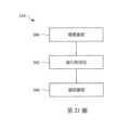
第19圖至第21圖為根據一些實施方式,繪示在形成互連結構的示例性方法期間的各個中間結構的截面圖。第19圖和第20圖繪示了在第4圖(例如,在操作202-208完成之後)的中間互連結構上清潔製程(方法200的操作210)的執行。根據此實施方式的清潔製程在第21圖中進一步詳細繪示。在此實施方式中,清潔製程包括電漿處理(操作260),接著是鹵化物浸泡(操作262),接著是還原處理(操作264)。19-21 are cross-sectional views illustrating various intermediate structures during an exemplary method of forming an interconnect structure, according to some embodiments. 19 and 20 illustrate performance of a cleaning process (
在所示的實施方式中,導電特徵24是多層的特徵,其包括由第一材料(例如,鈷)形成的主體24A,和由第二材料(例如,鎢)形成的蓋層24B。清潔製程清潔導電特徵24的蓋層24B。在一些實施方式中,諸如以上所述的那些,導電特徵24是單個連續的金屬層(例如,鎢)。In the illustrated embodiment,
第19圖繪示了電漿處理(操作260)和鹵物浸泡(操作262)的執行。使用電漿處理,以從溝槽40和或導孔開口42物理性地清除殘留物。使用鹵化物浸泡,以在處理期間移除在金屬特徵(例如,導電特徵24)上可能已形成的原生氧化物。Figure 19 depicts the performance of plasma treatment (operation 260) and halide soak (operation 262). Plasma treatment is used to physically remove residue from
電漿處理可以包括使用氫(H2)、氬(Ar)、氦(He)、氖(Ne)、O2、O3、N2、或NH3氣體,與載體氣體,諸如氬(Ar)。產生電漿鞘,並且加速氫穿過電漿鞘,以轟擊導孔開口42。在一些情況下,電漿處理可以減少殘留的氧化物、氮化物、和/或碳化物,其在用於圖案化第一蝕刻停止層26、第二介電層28、第二蝕刻停止層30、第三介電層32、和/或襯層50的蝕刻製程期間,可能形成在溝槽40和/或導孔開口42的側壁上和/或底表面上。電漿處理中的氫氣的流速可以在從約5sccm至約1,000sccm的範圍內,並且電漿處理中的載體氣體的流速可以在從約0sccm至約1,000sccm的範圍內。電漿處理的壓力可以在從約10毫托(mTorr)至約200毫托的範圍內。電漿處理的溫度可以在從約-20℃至約100℃的範圍內。電漿處理的電漿發生器的功率可以在從約20W至約400W的範圍內,並且電漿發生器的頻率可以是大約13.56MHz或更高。在電漿處理期間,基板可以加偏壓,在從約20V至約200V的範圍內。電漿處理可能執行短的持續時間。特別地,執行電漿處理可能持續至足以從溝槽40和/或導孔開口42物理性清除殘留物,但是可能執行時間不會長到足以移除在導電特徵24上可能已經形成的原生氧化物。例如,在一些實施方式中,電漿處理的持續時間可以在從約5秒至約300秒的範圍內。電漿處理執行短的持續時間減少了在電漿處理期間損壞導孔開口42的輪廓或導電特徵24的風險。Plasma treatment may include the use of hydrogen (H2 ), argon (Ar), helium (He), neon (Ne), O2 , O3 , N2 , or NH3 gases with a carrier gas such as argon (Ar) . A plasma sheath is created and hydrogen is accelerated through the plasma sheath to bombard via
鹵化物浸泡包括將導電特徵24暴露於一或多種浸泡劑。浸泡劑是導電特徵24的材料的鹵化物。在一些實施方式中,浸泡劑是導電特徵24的材料的氯化物或氟化物。例如,在導電特徵24是由鎢(W)形成的實施方式中,鹵化物六氟化鎢(WF6)。同樣地,在導電特徵24其上形成具有矽化物(例如,TiSi)的實施方式中,鹵化物可能是四氯化鈦(TiCl4)、四氟化鈦(TiF4)、或其組合。在一些實施方式中,用於形成導電特徵24的一或多種前趨物也可能用來作為浸泡劑。繼續導電特徵24由鎢形成的實施例,相同的前趨物(例如,WF6)可能用於導電特徵24的沉積也用於導電特徵24的浸泡。鹵化物浸泡在處理室中執行,在一些實施方式中,處理室是用於沉積導電特徵24的材料的相同處理室。鹵化物浸泡的壓力可以在從約1毫托至約10毫托的範圍內。鹵化物浸泡的溫度可以在從約300℃至約450℃的範圍內。鹵化物浸泡的持續時間可以在從約5秒至約120秒的範圍內。Halide soaking includes exposing
鹵化物浸泡移除在導電特徵24之上可能已形成的原生氧化物。特別地,鹵化物浸泡劑將固相原生氧化物轉化為氣相氧化物,然後將氣相氧化物從導孔開口42和溝槽40抽除。繼續導電特徵24由鎢形成的實施例,可能在製程期間在導電特徵24的暴露的表面上形成鎢氧化物,根據:W+1.5O2→WO3. (1)將鎢氧化物暴露在鹵化物浸泡劑中,將鎢氧化物轉化為鎢氧氟化物,根據:2WO3+WF6→3WO2F2. (2)然後可能從處理室中抽除所生成的鎢氧氟化物氣體。完成抽除可能經由例如使惰性氣體(例如氬)流過處理室,以帶走鎢氧氟化物。以鹵化物浸泡從導電特徵24的暴露的表面移除原生氧化物,可能減少在移除原生氧化物期間對導電特徵24造成的損壞。此外,鹵化物浸泡劑可能蝕刻導電特徵24而基本上不蝕刻第一蝕刻停止層26、第二介電層28、第二蝕刻停止層30、第三介電層32、或襯層50。因此,鹵化物浸泡可能允許清潔導電特徵24的暴露的表面而基本上不損壞導孔開口42的輪廓。清潔製程的製程窗口可能因此改善,特別是當導孔開口42的寬度小於約10奈米時。此外,避免損壞導孔開口42的輪廓可能減少在形成導電導孔60期間在導孔開口42內形成空隙的機會(參見第5圖)。The halide soak removes native oxide that may have formed over conductive features 24 . In particular, the halide soak converts the solid-phase native oxide to gas-phase oxide, which is then pumped from via opening 42 and
在鹵化物浸泡之後,一些殘留物112可能餘留在導孔開口42內。殘留物112可能是浸泡劑本身的殘留物,或者可能是浸泡的殘留副產物。繼續導電特徵24由鎢形成的實施例,殘留物112可能是WF6、W、F、或WO2F2。殘留物112可能沿著導孔開口42的側壁和/或底部。After the halide soak, some
第20圖繪示還原處理(操作264)的執行。還原處理包括將導電特徵24暴露於一或多種還原劑,諸如H2。暴露於還原劑允許導電特徵24的附加材料(例如,蓋層24B的材料)選擇性地再沉積在導孔開口42內。還原劑與殘留物112反應,諸如與殘留的鹵化物浸泡劑反應,以形成導電特徵24的附加材料。在導孔開口42內的殘留物112的量可能因此減少。繼續導電特徵24由鎢形成的實施例,鹵化物浸泡劑和殘留物112可能包括WF6,並且形成導電特徵24的附加材料可能根據:WF6+3H2→W+6HF. (3)還原處理可能在低壓和低溫下執行。還原處理的壓力可以在從約100毫托至約300毫托的範圍內。還原處理的溫度可以在從約300℃至約400℃的範圍內。還原處理的持續時間可以在從約5秒至約60秒的範圍內。Figure 20 illustrates execution of the restore process (operation 264). The reducing treatment includes exposing
導電特徵24的再沉積部分(例如,蓋層24B)至少部分向上延伸到導孔開口42內。導電特徵24的再沉積部分具有第十三尺寸,其從第一蝕刻停止層26的底表面至導電特徵24的頂表面。在一些實施例中,第十三尺寸D13,在從約2奈米至約15奈米的範圍內,例如小於約5奈米。在一些實施方式中,導電特徵24具有原始高度,原始高度具有第十四尺寸D14,在一些實施例中,第十四尺寸在從約10奈米至約50奈米的範圍內。第十三尺寸D13可能在第十四尺寸D14的約5%至約40%的範圍內。The redeposited portion of conductive feature 24 (eg,
在還原處理之後,可能執行如上所述的後續製程,以產生互連結構。這裡將不再重複進一步處理的細節。第22圖繪示了在後續製程之後(例如,在操作216-234完成之後),所得到的互連結構。第22圖的互連結構類似於第10圖的互連結構,並且包括一些浸泡劑的殘留物112在導電導孔60的周圍。此外,導電特徵24的再沉積部分接觸襯裡52的側壁的部分,並且襯裡52的底表面低於導電導孔60的底表面。導電特徵24和導電導孔60的界面可能低於、齊平、或高於第一蝕刻停止層26頂表面。雖然一些殘留物112被繪示為在導電特徵24和導電導孔60的界面處,但應當理解,在界面處的一些或全部的殘留物112可能經由還原處理(操作264)而消耗。導電導孔60的側壁可能具有比導電特徵24和導電導孔60的界面更多的殘留物112。在一些實施方式中,沒有殘留物112餘留在導電特徵24和導電導孔60的界面處。After the reduction process, subsequent processing may be performed as described above to produce the interconnect structure. Details of further processing will not be repeated here. FIG. 22 illustrates the resulting interconnect structure after subsequent processing (eg, after operations 216-234 are complete). The interconnect structure of FIG. 22 is similar to that of FIG. 10 and includes some
雖然所得到的第22圖的互連結構類似於第10圖的互連結構,應該理解的是,第21圖所繪示的清潔製程可能可適用於其他實施方式。例如,所得到的互連結構可能替代地類似於第13圖至第18圖的實施方式。Although the resulting interconnect structure of FIG. 22 is similar to that of FIG. 10, it should be understood that the cleaning process depicted in FIG. 21 may be applicable to other embodiments. For example, the resulting interconnect structure may alternatively be similar to the embodiments of FIGS. 13-18 .
一些實施方式可能實現優點。執行鹵化物浸泡以作為用於導孔開口42的清潔製程的部分,允許電漿處理的持續時間減少,這可能減少經由清潔製程對於導孔開口42的輪廓造成的損壞。在導電導孔60內形成空隙的機會可能因此減少。用鹵化物浸泡從導電特徵24移除原生氧化物,並且用還原處理再沉積導電特徵24的附加材料,可能產生乾淨的(例如,無氧化物)表面(導電導孔60可能在此表面上形成),降低了互連結構的電阻。如前所述,經由一些實施方式可能排除晶種層和/或阻障層。沒有晶種層和/或阻障層,互連結構的電阻可以減小,從而減小電阻電容(RC)延遲和增加裝置速度。此外,由於成核輔助處理的結果,在形成互連結構中導電填充材料的沉積可能是自底向上沉積和/或共形的沉積。自底向上沉積和/或共形的沉積可以減少填充溝槽所需的時間,這可以增加製程期間的處理量並降低成本。示例性的實施方式可能應用於任何技術節點,並且可能特別適用於諸如20奈米和更小的先進技術節點。Advantages may be realized by some implementations. Performing a halide soak as part of the cleaning process for the via
在一實施方式中,方法包括:蝕刻互連開口,其穿過在半導體基板上方的一或多個介電層,互連開口具有導孔開口和在導孔開口上方的溝槽,導孔開口暴露在半導體基板上方的導電特徵,導電特徵包括第一導電材料的第一層;用電漿處理導孔開口,以從導孔開口的側壁和底部物理性地移除蝕刻殘留物;用第一導電材料的鹵化物浸泡導電特徵,浸泡之後,第一導電材料的殘留鹵化物餘留在導孔開口內;減少第一導電材料的殘留鹵化物,以在第一層上形成第一導電材料的第二層;在第一導電材料的第二層上的導孔開口內沉積導電導孔;以及在溝槽的一或多個暴露的介電質表面上和導電導孔上在溝槽內形成導電線。In one embodiment, a method includes etching an interconnect opening through one or more dielectric layers above a semiconductor substrate, the interconnect opening having a via opening and a trench over the via opening, the via opening a conductive feature exposed above the semiconductor substrate, the conductive feature comprising a first layer of a first conductive material; treating the via opening with a plasma to physically remove etch residue from the sidewalls and bottom of the via opening; using a first The halide of the conductive material soaks the conductive feature, after soaking, the residual halide of the first conductive material remains in the via opening; the residual halide of the first conductive material is reduced to form the first conductive material on the first layer. second layer; depositing a conductive via within the via opening on the second layer of first conductive material; and forming within the trench on one or more exposed dielectric surfaces of the trench and on the conductive via conductive thread.
在方法的一些實施方式中,第一導電材料是鎢,第一導電材料的鹵化物是六氟化鎢。在方法的一些實施方式中,減少第一導電材料的殘留鹵化物包括將殘留的鹵化物暴露於氫。在方法的一些實施方式中,形成導電線包括在一或多個暴露的介電質表面上在溝槽內共形地沉積導電線的材料。在方法的一些實施方式中,沉積導電線的材料不包括沉積用於導電線的材料的晶種層。在方法的一些實施方式中,在沉積導電線的材料之前,在互連開口內沒有沉積含金屬的阻障層。在一些實施方式中,方法更包括:在沉積導電線的材料之前,在溝槽的一或多個暴露的介電質表面上執行成核輔助處理。在方法的一些實施方式中,成核輔助處理經由破壞在溝槽內暴露的介電層的表面的化學鍵,在溝槽內暴露的介電層的表面上增加許多成核位點。In some embodiments of the method, the first conductive material is tungsten and the halide of the first conductive material is tungsten hexafluoride. In some embodiments of the method, reducing the residual halide of the first conductive material includes exposing the residual halide to hydrogen. In some embodiments of the method, forming the conductive line includes conformally depositing a material of the conductive line within the trench on the one or more exposed dielectric surfaces. In some embodiments of the method, depositing the material of the conductive lines does not include depositing a seed layer of the material for the conductive lines. In some embodiments of the method, no metal-containing barrier layer is deposited within the interconnect openings prior to depositing the material of the conductive lines. In some embodiments, the method further includes performing a nucleation assist treatment on the one or more exposed dielectric surfaces of the trenches prior to depositing the material of the conductive lines. In some embodiments of the method, the nucleation assisting treatment increases a number of nucleation sites on the surface of the dielectric layer exposed within the trench by breaking chemical bonds on the surface of the dielectric layer exposed within the trench.
在一實施方式中,方法包括:蝕刻互連開口,其穿過在半導體基板上方的一或多個介電層,互連開口具有導孔開口和在導孔開口上方的溝槽,導孔開口暴露在半導體基板上方的導電特徵,導電特徵包括導電材料;清潔導孔開口;在清潔過的導孔開口內沉積導電導孔;在溝槽的一或多個暴露的介電質表面上執行成核輔助處理;以及在溝槽的一或多個暴露的介電質表面上和在導電導孔上在溝槽內形成導電線。In one embodiment, a method includes etching an interconnect opening through one or more dielectric layers above a semiconductor substrate, the interconnect opening having a via opening and a trench over the via opening, the via opening A conductive feature exposed over a semiconductor substrate, the conductive feature comprising a conductive material; cleaning the via opening; depositing a conductive via within the cleaned via opening; performing the forming process on one or more exposed dielectric surfaces of the trench. core assisted processing; and forming conductive lines within the trenches on the one or more exposed dielectric surfaces of the trenches and on the conductive vias.
在方法的一些實施方式中,清潔導孔開口包括:用導電材料的鹵化物清潔導孔開口。在方法的一些實施方式中,蝕刻互連開口,在導孔開口內形成蝕刻殘留物,和在導電特徵的表面上形成原生氧化物,並且清潔導孔開口包括:經由用電漿處理導孔開口,移除蝕刻殘留物;以及經由暴露導電特徵的表面於導電材料的鹵化物,移除原生氧化物。在方法的一些實施方式中,用電漿處理導孔開口包括:用氫氣轟擊導孔開口,持續約5秒至約300秒。在方法的一些實施方式中,暴露導電特徵的表面包括:用導電材料的鹵化物浸泡導電特徵的表面,在浸泡之後殘留的鹵化物餘留在導孔開口內。在一些實施方式中,方法更包括:經由將導電特徵的表面暴露於還原劑,在導電特徵上再沉積附加的導電材料。在方法的一些實施方式中,將導電特徵的表面暴露於還原劑包括:用氫還原殘留的鹵化物,還原的殘留的鹵化物形成附加的導電材料。在一些實施方式中,方法更包括:用複數個用於導電材料的前趨物在半導體基板上方沉積導電特徵,導電材料的鹵化物是用於導電材料的前趨物之一。在方法的一些實施方式中,成核輔助處理經由破壞溝槽的暴露的介電質表面的化學鍵,在溝槽的暴露的介電質表面上的增加多個成核位點。在方法的一些實施方式中,形成導電線包括在溝槽的暴露的介電質表面上在溝槽內共形地沉積導電線的材料,而不沉積用於導電線的材料的晶種層。In some embodiments of the method, cleaning the via opening includes cleaning the via opening with a halide of a conductive material. In some embodiments of the method, etching the interconnect opening, forming an etch residue within the via opening, and forming a native oxide on the surface of the conductive feature, and cleaning the via opening includes: treating the via opening with a plasma , removing etch residues; and removing native oxide by exposing the surface of the conductive feature to the halide of the conductive material. In some embodiments of the method, plasma treating the via opening includes bombarding the via opening with hydrogen gas for about 5 seconds to about 300 seconds. In some embodiments of the method, exposing the surface of the conductive feature includes soaking the surface of the conductive feature with a halide of the conductive material, residual halide remaining within the via opening after soaking. In some embodiments, the method further includes redepositing additional conductive material on the conductive feature via exposing the surface of the conductive feature to a reducing agent. In some embodiments of the method, exposing the surface of the conductive feature to the reducing agent includes reducing the residual halide with hydrogen, the reduced residual halide forming additional conductive material. In some embodiments, the method further includes depositing a conductive material over the semiconductor substrate with a plurality of precursors for the conductive material.Characteristically, halides of conductive materials are one of the precursors for conductive materials. In some embodiments of the method, the nucleation assisting treatment increases a plurality of nucleation sites on the exposed dielectric surface of the trench by breaking chemical bonds on the exposed dielectric surface of the trench. In some embodiments of the method, forming the conductive line includes conformally depositing the material of the conductive line within the trench on the exposed dielectric surface of the trench without depositing a seed layer of the material for the conductive line.
在一實施方式中,方法包括:在基板上方沉積導電特徵,沉積包括提供用於第一導電材料的複數個前趨物;在導電特徵上方沉積一或多個介電層;蝕刻互留開口,其穿過一或多個介電層蝕,互連開口具有導孔部分和在導孔部分上方的線部分;用第一導電材料的鹵化物清潔互連開口的側壁和底表面,第一導電材料的鹵化物是用於第一導電材料的前趨物之一。在清潔過的互連開口的導孔部分內沉積導電導孔,導電導孔接觸導電特徵;以及在清潔過的互連開口的線部分內沉積導電線。In one embodiment, a method includes: depositing a conductive feature over a substrate, the depositing comprising providing a plurality of precursors for a first conductive material; depositing one or more dielectric layers over the conductive feature; etching mutual openings, It is etched through one or more dielectric layers, the interconnect opening has a via portion and a line portion above the via portion; the sidewalls and bottom surface of the interconnect opening are cleaned with a halide of a first conductive material, the first conductive The halide of the material is one of the precursors for the first conductive material. Depositing a conductive via in the via portion of the cleaned interconnect opening, the conductive via contacting the conductive feature; and depositing a conductive line in the line portion of the cleaned interconnect opening.
在一些實施方式中,方法更包括:在清潔互連開口之後,在清潔過的互連開口內的導電特徵上沉積第一導電材料的層。In some embodiments, the method further includes, after cleaning the interconnect opening, depositing a layer of the first conductive material on the conductive features within the cleaned interconnect opening.
本揭示內容的一些實施方式提供了一種半導體裝置的製造方法,包含:蝕刻互連開口,其穿過在半導體基板上方的一或多個介電層,互連開口具有導孔開口和在導孔開口上方的溝槽,導孔開口暴露在半導體基板上方的導電特徵,導電特徵包含第一導電材料的第一層;用電漿處理導孔開口,以從導孔開口的側壁和底部物理性地移除蝕刻殘留物;以第一導電材料的鹵化物浸泡導電特徵,在浸泡之後,第一導電材料的殘留鹵化物餘留在導孔開口內;減少第一導電材料的殘留鹵化物,以在第一層上形成第一導電材料的第二層;在第一導電材料的第二層上的導孔開口內沉積導電導孔;以及在溝槽的一或多個暴露的介電質表面上和在導電導孔上在溝槽內形成導電線。Some embodiments of the present disclosure provide a method of fabricating a semiconductor device, comprising: etching an interconnection opening through one or more dielectric layers above a semiconductor substrate, the interconnection opening having a via opening and a via opening trench over the opening, the via opening exposing a conductive feature above the semiconductor substrate, the conductive feature comprising a first layer of a first conductive material; plasma treating the via opening to physically remove Remove etch residueThe conductive feature is soaked with the halide of the first conductive material, after soaking, the residual halide of the first conductive material remains in the via opening; the residual halide of the first conductive material is reduced to form on the first layer forming a second layer of first conductive material; depositing a conductive via within the via opening on the second layer of first conductive material; Conductive lines are formed on the holes within the trenches.
在一些實施方式中,其中第一導電材料是鎢,並且第一導電材料的鹵化物是六氟化鎢。In some embodiments, wherein the first conductive material is tungsten, and the halide of the first conductive material is tungsten hexafluoride.
在一些實施方式中,其中減少第一導電材料的殘留鹵化物包含將殘留的鹵化物暴露於氫。In some embodiments, wherein reducing the residual halide of the first conductive material comprises exposing the residual halide to hydrogen.
在一些實施方式中,其中形成導電線包含在所述一或多個暴露的表面上在溝槽內共形地沉積導電線的材料。In some embodiments, wherein forming the conductive line comprises conformally depositing a material of the conductive line within the trench on the one or more exposed surfaces.
在一些實施方式中,其中沉積導電線的材料不包括沉積用於沉積導線的材料的晶種層。In some embodiments, wherein depositing the material of the conductive lines does not include depositing a seed layer of the material used to deposit the lines.
在一些實施方式中,其中在沉積導電線的材料之前,在互連開口內沒有沉積含金屬的阻障層。In some embodiments, wherein no metal-containing barrier layer is deposited within the interconnect openings prior to depositing the material of the conductive lines.
在一些實施方式中,更包含:在沉積導電線的材料之前,在溝槽的一或多個暴露的介電質表面上執行成核輔助處理。In some embodiments, further comprising: performing a nucleation assist treatment on one or more exposed dielectric surfaces of the trenches prior to depositing the material of the conductive lines.
在一些實施方式中,其中成核輔助處理經由破壞在溝槽內暴露的介電層的表面上的化學鍵,在溝槽內暴露的介電層的表面上增加多個成核位點。In some embodiments, wherein the nucleation assisting treatment increases a plurality of nucleation sites on the surface of the dielectric layer exposed in the trench by breaking chemical bonds on the surface of the dielectric layer exposed in the trench.
本揭示內容的一些實施方式提供了一種方法,包含:蝕刻互連開口,其穿過在半導體基板上方的一或多個介電層,互連開口具有導孔開口和在導孔開口上方的溝槽,導孔開口暴露在半導體基板上方的導電特徵,導電特徵包含導電材料;清潔導孔開口;沉積導電導孔,其在清潔過的導孔開口內;在溝槽的一或多個暴露的介電質表面上執行成核輔助處理;以及在溝槽內形成導電線,其在溝槽的一或多個暴露的介電質表面上和導電導孔上。Some embodiments of the present disclosure provide a method,Comprising: etching an interconnect opening through one or more dielectric layers over a semiconductor substrate, the interconnect opening having a via opening and a trench over the via opening, the via opening exposing a conductive layer over the semiconductor substrate. feature, the conductive feature comprises a conductive material; cleaning the via opening; depositing a conductive via within the cleaned via opening; performing a nucleation assist process on one or more exposed dielectric surfaces of the trench; and Conductive lines are formed within the trench, on one or more exposed dielectric surfaces of the trench and on the conductive vias.
在一些實施方式中,其中清潔導孔開口包含:以導電材料的鹵化物清潔導孔開口。In some embodiments, cleaning the via opening includes: cleaning the via opening with a halide of a conductive material.
在一些實施方式中,其中蝕刻互連開口,在導孔開口內形成蝕刻殘留物和在導電特徵的表面上形成原生氧化物,以及清潔導孔開口包含:經由利用電漿處理導孔開口來移除蝕刻殘留物;以及經由暴露導電特徵的表面於導電材料的鹵化物,移除原生氧化物。In some embodiments, wherein the interconnect opening is etched, etch residues are formed within the via opening and native oxide is formed on the surface of the conductive feature, and cleaning the via opening comprises removing the via opening by treating the via opening with a plasma. removing etch residue; and removing native oxide by exposing the surface of the conductive feature to the halide of the conductive material.
在一些實施方式中,其中以電漿處理導孔開口包含:用氫氣轟擊導孔開口,持續從約5秒至約300秒。In some embodiments, treating the via opening with the plasma comprises: bombarding the via opening with hydrogen gas for from about 5 seconds to about 300 seconds.
在一些實施方式中,其中暴露導電特徵的表面包含:用導電材料的鹵化物浸泡導電特徵的表面,在浸泡之後殘留的鹵化物餘留在導孔開口內。In some embodiments, wherein exposing the surface of the conductive feature comprises soaking the surface of the conductive feature with a halide of the conductive material, residual halide remaining within the via opening after soaking.
在一些實施方式中,更包含:經由將導電特徵的表面暴露於還原劑,在導電特徵上再沉積附加的導電材料。In some embodiments, further comprising redepositing additional conductive material on the conductive feature by exposing the surface of the conductive feature to a reducing agent.
在一些實施方式中,其中將導電特徵的表面暴露於還原劑包含:用氫還原殘留的鹵化物,還原的殘留的鹵化物形成附加的導電材料。In some embodiments, wherein exposing the surface of the conductive feature to the reducing agent comprises: reducing the residual halide with hydrogen, the reduced residual halideThe compound forms an additional conductive material.
在一些實施方式中,更包含:用多個用於導電材料的前趨物在半導體基板上方沉積導電特徵,導電材料的鹵化物是用於導電材料的前趨物之一。In some embodiments, further comprising: depositing a conductive feature over the semiconductor substrate with a plurality of precursors for the conductive material, the halide of the conductive material being one of the precursors for the conductive material.
在一些實施方式中,其中成核輔助處理經由破壞溝槽的暴露的介電質表面的化學鍵,在溝槽的暴露的介電質表面上增加多個成核位點。In some embodiments, wherein the nucleation assisting treatment increases a plurality of nucleation sites on the exposed dielectric surface of the trench by breaking chemical bonds on the exposed dielectric surface of the trench.
在一些實施方式中,其中形成導電線包含在溝槽的暴露的介電質表面上共形地沉積導電線的材料,而不沉積用於導電線的材料的晶種層。In some embodiments, wherein forming the conductive line includes conformally depositing the material of the conductive line on the exposed dielectric surface of the trench without depositing a seed layer of the material for the conductive line.
本揭示內容的一些實施方式提供了一種方法,包含:在基板上方沉積導電特徵,沉積包含提供用於第一導電材料的複數個前趨物;在導電特徵上方沉積一或多個介電層;蝕刻互連開口,其穿過一或多個介電層,互連開口具有導孔部分和在導孔部分上方的線部分;用第一導電材料的鹵化物清潔互連開口的側壁和底表面,第一導電材料的鹵化物是用於第一導電材料的前趨物之一。在清潔過的互連開口的導孔部分內沉積導電導孔,導電導孔接觸導電特徵;以及在清潔過的互連開口的線部分內沉積導電線。Some embodiments of the present disclosure provide a method comprising: depositing a conductive feature over a substrate, the depositing comprising providing a plurality of precursors for a first conductive material; depositing one or more dielectric layers over the conductive feature; etching an interconnect opening through the one or more dielectric layers, the interconnect opening having a via portion and a line portion over the via portion; cleaning sidewalls and a bottom surface of the interconnect opening with a halide of a first conductive material , the halide of the first conductive material is one of the precursors for the first conductive material. Depositing a conductive via in the via portion of the cleaned interconnect opening, the conductive via contacting the conductive feature; and depositing a conductive line in the line portion of the cleaned interconnect opening.
在一些實施方式中,更包含:在清潔互連開口之後,在清潔過的互連開口內的導電特徵上沉積第一導電材料的層。In some embodiments, further comprising: after cleaning the interconnect opening, depositing a layer of the first conductive material on the conductive features within the cleaned interconnect opening.
以上概述了數個實施方式,以便本領域技術人員可以較佳地理解本揭示內容的各方面。本領域的技術人員應理解,他們可能容易地使用本揭示內容,作為其他製程和結構之設計和修改的基礎,以實現與在此介紹的實施方式的相同的目的,或是達到相同的優點。本領域技術人員亦應理解,與這些均等的建構不脫離本揭示內容的精神和範圍,並且他們可能在不脫離本揭示內容的精神和範圍的情況下,進行各種改變、替換、和變更。Several implementations have been outlined above so that those skilled in the art can better understand aspects of the present disclosure. those skilled in the artIt should be understood that they may readily use the present disclosure as a basis for the design and modification of other processes and structures to achieve the same purposes, or to achieve the same advantages, as the embodiments presented herein. Those skilled in the art should also understand that these equivalent constructions do not depart from the spirit and scope of the present disclosure, and that they may make various changes, substitutions and alterations herein without departing from the spirit and scope of the present disclosure.
200:方法200: method
202、204、206、208、210、212、214、216、218、220、222、224、226、228、230、232、234:操作202, 204, 206, 208, 210, 212, 214, 216, 218, 220, 222, 224, 226, 228, 230, 232, 234: operation
Claims (10)
Translated fromChineseApplications Claiming Priority (6)
| Application Number | Priority Date | Filing Date | Title |
|---|---|---|---|
| US201862757971P | 2018-11-09 | 2018-11-09 | |
| US62/757,971 | 2018-11-09 | ||
| US201862774637P | 2018-12-03 | 2018-12-03 | |
| US62/774,637 | 2018-12-03 | ||
| US16/354,362 | 2019-03-15 | ||
| US16/354,362US11011413B2 (en) | 2017-11-30 | 2019-03-15 | Interconnect structures and methods of forming the same |
Publications (2)
| Publication Number | Publication Date |
|---|---|
| TW202018808A TW202018808A (en) | 2020-05-16 |
| TWI801631Btrue TWI801631B (en) | 2023-05-11 |
Family
ID=70621514
Family Applications (1)
| Application Number | Title | Priority Date | Filing Date |
|---|---|---|---|
| TW108125489ATWI801631B (en) | 2018-11-09 | 2019-07-18 | Semiconductor device manufacturing method and semiconductor device |
Country Status (2)
| Country | Link |
|---|---|
| CN (1) | CN111180384B (en) |
| TW (1) | TWI801631B (en) |
Families Citing this family (1)
| Publication number | Priority date | Publication date | Assignee | Title |
|---|---|---|---|---|
| CN115513173B (en)* | 2021-06-23 | 2025-08-22 | 中芯国际集成电路制造(上海)有限公司 | Semiconductor structure and method for forming semiconductor structure |
Citations (1)
| Publication number | Priority date | Publication date | Assignee | Title |
|---|---|---|---|---|
| US20130200525A1 (en)* | 2012-02-02 | 2013-08-08 | Ho-Jin Lee | Via connection structures, semiconductor devices having the same, and methods of fabricating the structures and devices |
Family Cites Families (7)
| Publication number | Priority date | Publication date | Assignee | Title |
|---|---|---|---|---|
| US6731007B1 (en)* | 1997-08-29 | 2004-05-04 | Hitachi, Ltd. | Semiconductor integrated circuit device with vertically stacked conductor interconnections |
| US6087251A (en)* | 1998-10-30 | 2000-07-11 | United Microelectronics Corp. | Method of fabricating a dual damascene structure |
| US7335588B2 (en)* | 2005-04-15 | 2008-02-26 | International Business Machines Corporation | Interconnect structure and method of fabrication of same |
| US9218980B2 (en)* | 2013-09-13 | 2015-12-22 | Applied Materials, Inc. | Surface treatment to improve CCTBA based CVD co nucleation on dielectric substrate |
| US9318439B2 (en)* | 2014-03-21 | 2016-04-19 | Taiwan Semiconductor Manufacturing Company Ltd. | Interconnect structure and manufacturing method thereof |
| US9837309B2 (en)* | 2015-11-19 | 2017-12-05 | International Business Machines Corporation | Semiconductor via structure with lower electrical resistance |
| US9536780B1 (en)* | 2016-04-15 | 2017-01-03 | International Business Machines Corporation | Method and apparatus for single chamber treatment |
- 2019
- 2019-07-18TWTW108125489Apatent/TWI801631B/enactive
- 2019-11-11CNCN201911093292.7Apatent/CN111180384B/enactiveActive
Patent Citations (1)
| Publication number | Priority date | Publication date | Assignee | Title |
|---|---|---|---|---|
| US20130200525A1 (en)* | 2012-02-02 | 2013-08-08 | Ho-Jin Lee | Via connection structures, semiconductor devices having the same, and methods of fabricating the structures and devices |
Also Published As
| Publication number | Publication date |
|---|---|
| CN111180384A (en) | 2020-05-19 |
| CN111180384B (en) | 2024-02-23 |
| TW202018808A (en) | 2020-05-16 |
Similar Documents
| Publication | Publication Date | Title |
|---|---|---|
| TWI706508B (en) | Semiconductor device manufacturing method and structure | |
| US11011413B2 (en) | Interconnect structures and methods of forming the same | |
| TW201939666A (en) | Semiconductor structures and methods for semiconductor processing | |
| US8030205B2 (en) | Method for fabricating semiconductor device with metal line | |
| US7670946B2 (en) | Methods to eliminate contact plug sidewall slit | |
| CN106548974A (en) | Semiconductor device and method for manufacturing the same | |
| CN110890315B (en) | Semiconductor structure with Damascus structure and preparation method thereof | |
| TW201937654A (en) | Method for forming semiconductor structures | |
| US20080174018A1 (en) | Semiconductor device and method for fabricating the same | |
| CN110943070B (en) | Semiconductor structure, semiconductor structure preparation method and use thereof | |
| US12347724B2 (en) | Surface modification layer for conductive feature formation | |
| CN106469674A (en) | Method for forming metal interconnection | |
| CN115472556A (en) | Method for forming interconnection structure | |
| US20170148735A1 (en) | Interconnect Structure for Semiconductor Devices | |
| TWI801631B (en) | Semiconductor device manufacturing method and semiconductor device | |
| US20230154845A1 (en) | Interconnect Structures | |
| KR100598187B1 (en) | Metal wiring formation method of semiconductor device |