TWI798443B - Ground path systems for providing a shorter and symmetrical ground path - Google Patents
Ground path systems for providing a shorter and symmetrical ground pathDownload PDFInfo
- Publication number
- TWI798443B TWI798443BTW108117843ATW108117843ATWI798443BTW I798443 BTWI798443 BTW I798443BTW 108117843 ATW108117843 ATW 108117843ATW 108117843 ATW108117843 ATW 108117843ATW I798443 BTWI798443 BTW I798443B
- Authority
- TW
- Taiwan
- Prior art keywords
- cup
- chamber
- processing
- coupled
- grounded
- Prior art date
Links
- 239000004020conductorSubstances0.000claimsdescription49
- 238000001816coolingMethods0.000claimsdescription23
- 239000000758substrateSubstances0.000claimsdescription18
- 238000005229chemical vapour depositionMethods0.000claimsdescription16
- 230000001902propagating effectEffects0.000claimsdescription10
- 230000004888barrier functionEffects0.000claimsdescription9
- 238000000034methodMethods0.000claimsdescription8
- 230000008569processEffects0.000claimsdescription8
- 230000003071parasitic effectEffects0.000abstractdescription14
- 239000007789gasSubstances0.000description34
- 238000000151depositionMethods0.000description8
- 230000008021depositionEffects0.000description8
- 229910001026inconelInorganic materials0.000description7
- 239000010935stainless steelSubstances0.000description7
- 229910001220stainless steelInorganic materials0.000description7
- PXHVJJICTQNCMI-UHFFFAOYSA-NNickelChemical compound[Ni]PXHVJJICTQNCMI-UHFFFAOYSA-N0.000description6
- 229910045601alloyInorganic materials0.000description6
- 239000000956alloySubstances0.000description6
- 230000015572biosynthetic processEffects0.000description6
- 239000000463materialSubstances0.000description6
- NJPPVKZQTLUDBO-UHFFFAOYSA-NnovaluronChemical compoundC1=C(Cl)C(OC(F)(F)C(OC(F)(F)F)F)=CC=C1NC(=O)NC(=O)C1=C(F)C=CC=C1FNJPPVKZQTLUDBO-UHFFFAOYSA-N0.000description5
- 230000008878couplingEffects0.000description4
- 238000010168coupling processMethods0.000description4
- 238000005859coupling reactionMethods0.000description4
- XAGFODPZIPBFFR-UHFFFAOYSA-NaluminiumChemical compound[Al]XAGFODPZIPBFFR-UHFFFAOYSA-N0.000description3
- 229910052782aluminiumInorganic materials0.000description3
- 238000000231atomic layer depositionMethods0.000description3
- 229910052759nickelInorganic materials0.000description3
- 230000008901benefitEffects0.000description2
- 239000006227byproductSubstances0.000description2
- 238000005240physical vapour depositionMethods0.000description2
- 238000000623plasma-assisted chemical vapour depositionMethods0.000description2
- RYGMFSIKBFXOCR-UHFFFAOYSA-NCopperChemical compound[Cu]RYGMFSIKBFXOCR-UHFFFAOYSA-N0.000description1
- ZOKXTWBITQBERF-UHFFFAOYSA-NMolybdenumChemical compound[Mo]ZOKXTWBITQBERF-UHFFFAOYSA-N0.000description1
- PNEYBMLMFCGWSK-UHFFFAOYSA-Naluminium oxideInorganic materials[O-2].[O-2].[O-2].[Al+3].[Al+3]PNEYBMLMFCGWSK-UHFFFAOYSA-N0.000description1
- 229910052802copperInorganic materials0.000description1
- 239000010949copperSubstances0.000description1
- PMHQVHHXPFUNSP-UHFFFAOYSA-Mcopper(1+);methylsulfanylmethane;bromideChemical compoundBr[Cu].CSCPMHQVHHXPFUNSP-UHFFFAOYSA-M0.000description1
- 230000005684electric fieldEffects0.000description1
- 238000010438heat treatmentMethods0.000description1
- 239000000203mixtureSubstances0.000description1
- 229910052750molybdenumInorganic materials0.000description1
- 239000011733molybdenumSubstances0.000description1
- 230000008520organizationEffects0.000description1
- 230000037361pathwayEffects0.000description1
- 239000002243precursorSubstances0.000description1
- 239000010453quartzSubstances0.000description1
- 239000004065semiconductorSubstances0.000description1
- VYPSYNLAJGMNEJ-UHFFFAOYSA-Nsilicon dioxideInorganic materialsO=[Si]=OVYPSYNLAJGMNEJ-UHFFFAOYSA-N0.000description1
- WFKWXMTUELFFGS-UHFFFAOYSA-NtungstenChemical compound[W]WFKWXMTUELFFGS-UHFFFAOYSA-N0.000description1
- 229910052721tungstenInorganic materials0.000description1
- 239000010937tungstenSubstances0.000description1
- 235000012431wafersNutrition0.000description1
Images


Classifications
- C—CHEMISTRY; METALLURGY
- C23—COATING METALLIC MATERIAL; COATING MATERIAL WITH METALLIC MATERIAL; CHEMICAL SURFACE TREATMENT; DIFFUSION TREATMENT OF METALLIC MATERIAL; COATING BY VACUUM EVAPORATION, BY SPUTTERING, BY ION IMPLANTATION OR BY CHEMICAL VAPOUR DEPOSITION, IN GENERAL; INHIBITING CORROSION OF METALLIC MATERIAL OR INCRUSTATION IN GENERAL
- C23C—COATING METALLIC MATERIAL; COATING MATERIAL WITH METALLIC MATERIAL; SURFACE TREATMENT OF METALLIC MATERIAL BY DIFFUSION INTO THE SURFACE, BY CHEMICAL CONVERSION OR SUBSTITUTION; COATING BY VACUUM EVAPORATION, BY SPUTTERING, BY ION IMPLANTATION OR BY CHEMICAL VAPOUR DEPOSITION, IN GENERAL
- C23C16/00—Chemical coating by decomposition of gaseous compounds, without leaving reaction products of surface material in the coating, i.e. chemical vapour deposition [CVD] processes
- C23C16/44—Chemical coating by decomposition of gaseous compounds, without leaving reaction products of surface material in the coating, i.e. chemical vapour deposition [CVD] processes characterised by the method of coating
- C23C16/50—Chemical coating by decomposition of gaseous compounds, without leaving reaction products of surface material in the coating, i.e. chemical vapour deposition [CVD] processes characterised by the method of coating using electric discharges
- C23C16/505—Chemical coating by decomposition of gaseous compounds, without leaving reaction products of surface material in the coating, i.e. chemical vapour deposition [CVD] processes characterised by the method of coating using electric discharges using radio frequency discharges
- C23C16/509—Chemical coating by decomposition of gaseous compounds, without leaving reaction products of surface material in the coating, i.e. chemical vapour deposition [CVD] processes characterised by the method of coating using electric discharges using radio frequency discharges using internal electrodes
- C—CHEMISTRY; METALLURGY
- C23—COATING METALLIC MATERIAL; COATING MATERIAL WITH METALLIC MATERIAL; CHEMICAL SURFACE TREATMENT; DIFFUSION TREATMENT OF METALLIC MATERIAL; COATING BY VACUUM EVAPORATION, BY SPUTTERING, BY ION IMPLANTATION OR BY CHEMICAL VAPOUR DEPOSITION, IN GENERAL; INHIBITING CORROSION OF METALLIC MATERIAL OR INCRUSTATION IN GENERAL
- C23C—COATING METALLIC MATERIAL; COATING MATERIAL WITH METALLIC MATERIAL; SURFACE TREATMENT OF METALLIC MATERIAL BY DIFFUSION INTO THE SURFACE, BY CHEMICAL CONVERSION OR SUBSTITUTION; COATING BY VACUUM EVAPORATION, BY SPUTTERING, BY ION IMPLANTATION OR BY CHEMICAL VAPOUR DEPOSITION, IN GENERAL
- C23C16/00—Chemical coating by decomposition of gaseous compounds, without leaving reaction products of surface material in the coating, i.e. chemical vapour deposition [CVD] processes
- C23C16/44—Chemical coating by decomposition of gaseous compounds, without leaving reaction products of surface material in the coating, i.e. chemical vapour deposition [CVD] processes characterised by the method of coating
- C23C16/4401—Means for minimising impurities, e.g. dust, moisture or residual gas, in the reaction chamber
- C23C16/4404—Coatings or surface treatment on the inside of the reaction chamber or on parts thereof
- C—CHEMISTRY; METALLURGY
- C23—COATING METALLIC MATERIAL; COATING MATERIAL WITH METALLIC MATERIAL; CHEMICAL SURFACE TREATMENT; DIFFUSION TREATMENT OF METALLIC MATERIAL; COATING BY VACUUM EVAPORATION, BY SPUTTERING, BY ION IMPLANTATION OR BY CHEMICAL VAPOUR DEPOSITION, IN GENERAL; INHIBITING CORROSION OF METALLIC MATERIAL OR INCRUSTATION IN GENERAL
- C23C—COATING METALLIC MATERIAL; COATING MATERIAL WITH METALLIC MATERIAL; SURFACE TREATMENT OF METALLIC MATERIAL BY DIFFUSION INTO THE SURFACE, BY CHEMICAL CONVERSION OR SUBSTITUTION; COATING BY VACUUM EVAPORATION, BY SPUTTERING, BY ION IMPLANTATION OR BY CHEMICAL VAPOUR DEPOSITION, IN GENERAL
- C23C16/00—Chemical coating by decomposition of gaseous compounds, without leaving reaction products of surface material in the coating, i.e. chemical vapour deposition [CVD] processes
- C23C16/44—Chemical coating by decomposition of gaseous compounds, without leaving reaction products of surface material in the coating, i.e. chemical vapour deposition [CVD] processes characterised by the method of coating
- C23C16/455—Chemical coating by decomposition of gaseous compounds, without leaving reaction products of surface material in the coating, i.e. chemical vapour deposition [CVD] processes characterised by the method of coating characterised by the method used for introducing gases into reaction chamber or for modifying gas flows in reaction chamber
- C23C16/45523—Pulsed gas flow or change of composition over time
- C23C16/45525—Atomic layer deposition [ALD]
- C23C16/45527—Atomic layer deposition [ALD] characterized by the ALD cycle, e.g. different flows or temperatures during half-reactions, unusual pulsing sequence, use of precursor mixtures or auxiliary reactants or activations
- C23C16/45536—Use of plasma, radiation or electromagnetic fields
- C—CHEMISTRY; METALLURGY
- C23—COATING METALLIC MATERIAL; COATING MATERIAL WITH METALLIC MATERIAL; CHEMICAL SURFACE TREATMENT; DIFFUSION TREATMENT OF METALLIC MATERIAL; COATING BY VACUUM EVAPORATION, BY SPUTTERING, BY ION IMPLANTATION OR BY CHEMICAL VAPOUR DEPOSITION, IN GENERAL; INHIBITING CORROSION OF METALLIC MATERIAL OR INCRUSTATION IN GENERAL
- C23C—COATING METALLIC MATERIAL; COATING MATERIAL WITH METALLIC MATERIAL; SURFACE TREATMENT OF METALLIC MATERIAL BY DIFFUSION INTO THE SURFACE, BY CHEMICAL CONVERSION OR SUBSTITUTION; COATING BY VACUUM EVAPORATION, BY SPUTTERING, BY ION IMPLANTATION OR BY CHEMICAL VAPOUR DEPOSITION, IN GENERAL
- C23C16/00—Chemical coating by decomposition of gaseous compounds, without leaving reaction products of surface material in the coating, i.e. chemical vapour deposition [CVD] processes
- C23C16/44—Chemical coating by decomposition of gaseous compounds, without leaving reaction products of surface material in the coating, i.e. chemical vapour deposition [CVD] processes characterised by the method of coating
- C23C16/455—Chemical coating by decomposition of gaseous compounds, without leaving reaction products of surface material in the coating, i.e. chemical vapour deposition [CVD] processes characterised by the method of coating characterised by the method used for introducing gases into reaction chamber or for modifying gas flows in reaction chamber
- C23C16/45523—Pulsed gas flow or change of composition over time
- C23C16/45525—Atomic layer deposition [ALD]
- C23C16/45544—Atomic layer deposition [ALD] characterized by the apparatus
- C—CHEMISTRY; METALLURGY
- C23—COATING METALLIC MATERIAL; COATING MATERIAL WITH METALLIC MATERIAL; CHEMICAL SURFACE TREATMENT; DIFFUSION TREATMENT OF METALLIC MATERIAL; COATING BY VACUUM EVAPORATION, BY SPUTTERING, BY ION IMPLANTATION OR BY CHEMICAL VAPOUR DEPOSITION, IN GENERAL; INHIBITING CORROSION OF METALLIC MATERIAL OR INCRUSTATION IN GENERAL
- C23C—COATING METALLIC MATERIAL; COATING MATERIAL WITH METALLIC MATERIAL; SURFACE TREATMENT OF METALLIC MATERIAL BY DIFFUSION INTO THE SURFACE, BY CHEMICAL CONVERSION OR SUBSTITUTION; COATING BY VACUUM EVAPORATION, BY SPUTTERING, BY ION IMPLANTATION OR BY CHEMICAL VAPOUR DEPOSITION, IN GENERAL
- C23C16/00—Chemical coating by decomposition of gaseous compounds, without leaving reaction products of surface material in the coating, i.e. chemical vapour deposition [CVD] processes
- C23C16/44—Chemical coating by decomposition of gaseous compounds, without leaving reaction products of surface material in the coating, i.e. chemical vapour deposition [CVD] processes characterised by the method of coating
- C23C16/458—Chemical coating by decomposition of gaseous compounds, without leaving reaction products of surface material in the coating, i.e. chemical vapour deposition [CVD] processes characterised by the method of coating characterised by the method used for supporting substrates in the reaction chamber
- C23C16/4581—Chemical coating by decomposition of gaseous compounds, without leaving reaction products of surface material in the coating, i.e. chemical vapour deposition [CVD] processes characterised by the method of coating characterised by the method used for supporting substrates in the reaction chamber characterised by material of construction or surface finish of the means for supporting the substrate
- C—CHEMISTRY; METALLURGY
- C23—COATING METALLIC MATERIAL; COATING MATERIAL WITH METALLIC MATERIAL; CHEMICAL SURFACE TREATMENT; DIFFUSION TREATMENT OF METALLIC MATERIAL; COATING BY VACUUM EVAPORATION, BY SPUTTERING, BY ION IMPLANTATION OR BY CHEMICAL VAPOUR DEPOSITION, IN GENERAL; INHIBITING CORROSION OF METALLIC MATERIAL OR INCRUSTATION IN GENERAL
- C23C—COATING METALLIC MATERIAL; COATING MATERIAL WITH METALLIC MATERIAL; SURFACE TREATMENT OF METALLIC MATERIAL BY DIFFUSION INTO THE SURFACE, BY CHEMICAL CONVERSION OR SUBSTITUTION; COATING BY VACUUM EVAPORATION, BY SPUTTERING, BY ION IMPLANTATION OR BY CHEMICAL VAPOUR DEPOSITION, IN GENERAL
- C23C16/00—Chemical coating by decomposition of gaseous compounds, without leaving reaction products of surface material in the coating, i.e. chemical vapour deposition [CVD] processes
- C23C16/44—Chemical coating by decomposition of gaseous compounds, without leaving reaction products of surface material in the coating, i.e. chemical vapour deposition [CVD] processes characterised by the method of coating
- C23C16/458—Chemical coating by decomposition of gaseous compounds, without leaving reaction products of surface material in the coating, i.e. chemical vapour deposition [CVD] processes characterised by the method of coating characterised by the method used for supporting substrates in the reaction chamber
- C23C16/4582—Rigid and flat substrates, e.g. plates or discs
- C23C16/4583—Rigid and flat substrates, e.g. plates or discs the substrate being supported substantially horizontally
- C23C16/4586—Elements in the interior of the support, e.g. electrodes, heating or cooling devices
- C—CHEMISTRY; METALLURGY
- C23—COATING METALLIC MATERIAL; COATING MATERIAL WITH METALLIC MATERIAL; CHEMICAL SURFACE TREATMENT; DIFFUSION TREATMENT OF METALLIC MATERIAL; COATING BY VACUUM EVAPORATION, BY SPUTTERING, BY ION IMPLANTATION OR BY CHEMICAL VAPOUR DEPOSITION, IN GENERAL; INHIBITING CORROSION OF METALLIC MATERIAL OR INCRUSTATION IN GENERAL
- C23C—COATING METALLIC MATERIAL; COATING MATERIAL WITH METALLIC MATERIAL; SURFACE TREATMENT OF METALLIC MATERIAL BY DIFFUSION INTO THE SURFACE, BY CHEMICAL CONVERSION OR SUBSTITUTION; COATING BY VACUUM EVAPORATION, BY SPUTTERING, BY ION IMPLANTATION OR BY CHEMICAL VAPOUR DEPOSITION, IN GENERAL
- C23C16/00—Chemical coating by decomposition of gaseous compounds, without leaving reaction products of surface material in the coating, i.e. chemical vapour deposition [CVD] processes
- C23C16/44—Chemical coating by decomposition of gaseous compounds, without leaving reaction products of surface material in the coating, i.e. chemical vapour deposition [CVD] processes characterised by the method of coating
- C23C16/50—Chemical coating by decomposition of gaseous compounds, without leaving reaction products of surface material in the coating, i.e. chemical vapour deposition [CVD] processes characterised by the method of coating using electric discharges
- C23C16/505—Chemical coating by decomposition of gaseous compounds, without leaving reaction products of surface material in the coating, i.e. chemical vapour deposition [CVD] processes characterised by the method of coating using electric discharges using radio frequency discharges
- H—ELECTRICITY
- H01—ELECTRIC ELEMENTS
- H01J—ELECTRIC DISCHARGE TUBES OR DISCHARGE LAMPS
- H01J37/00—Discharge tubes with provision for introducing objects or material to be exposed to the discharge, e.g. for the purpose of examination or processing thereof
- H01J37/32—Gas-filled discharge tubes
- H01J37/32009—Arrangements for generation of plasma specially adapted for examination or treatment of objects, e.g. plasma sources
- H01J37/32082—Radio frequency generated discharge
- H01J37/32091—Radio frequency generated discharge the radio frequency energy being capacitively coupled to the plasma
- H—ELECTRICITY
- H01—ELECTRIC ELEMENTS
- H01J—ELECTRIC DISCHARGE TUBES OR DISCHARGE LAMPS
- H01J37/00—Discharge tubes with provision for introducing objects or material to be exposed to the discharge, e.g. for the purpose of examination or processing thereof
- H01J37/32—Gas-filled discharge tubes
- H01J37/32009—Arrangements for generation of plasma specially adapted for examination or treatment of objects, e.g. plasma sources
- H01J37/32082—Radio frequency generated discharge
- H01J37/32174—Circuits specially adapted for controlling the RF discharge
- H—ELECTRICITY
- H01—ELECTRIC ELEMENTS
- H01J—ELECTRIC DISCHARGE TUBES OR DISCHARGE LAMPS
- H01J37/00—Discharge tubes with provision for introducing objects or material to be exposed to the discharge, e.g. for the purpose of examination or processing thereof
- H01J37/32—Gas-filled discharge tubes
- H01J37/32431—Constructional details of the reactor
- H01J37/32532—Electrodes
- H01J37/32587—Triode systems
- H—ELECTRICITY
- H01—ELECTRIC ELEMENTS
- H01J—ELECTRIC DISCHARGE TUBES OR DISCHARGE LAMPS
- H01J37/00—Discharge tubes with provision for introducing objects or material to be exposed to the discharge, e.g. for the purpose of examination or processing thereof
- H01J37/32—Gas-filled discharge tubes
- H01J37/32431—Constructional details of the reactor
- H01J37/32715—Workpiece holder
- H01J37/32724—Temperature
- H—ELECTRICITY
- H01—ELECTRIC ELEMENTS
- H01J—ELECTRIC DISCHARGE TUBES OR DISCHARGE LAMPS
- H01J37/00—Discharge tubes with provision for introducing objects or material to be exposed to the discharge, e.g. for the purpose of examination or processing thereof
- H01J37/32—Gas-filled discharge tubes
- H01J37/32431—Constructional details of the reactor
- H01J37/32798—Further details of plasma apparatus not provided for in groups H01J37/3244 - H01J37/32788; special provisions for cleaning or maintenance of the apparatus
- H01J37/32816—Pressure
- H01J37/32834—Exhausting
- H—ELECTRICITY
- H01—ELECTRIC ELEMENTS
- H01L—SEMICONDUCTOR DEVICES NOT COVERED BY CLASS H10
- H01L21/00—Processes or apparatus adapted for the manufacture or treatment of semiconductor or solid state devices or of parts thereof
- H01L21/67—Apparatus specially adapted for handling semiconductor or electric solid state devices during manufacture or treatment thereof; Apparatus specially adapted for handling wafers during manufacture or treatment of semiconductor or electric solid state devices or components ; Apparatus not specifically provided for elsewhere
- H01L21/683—Apparatus specially adapted for handling semiconductor or electric solid state devices during manufacture or treatment thereof; Apparatus specially adapted for handling wafers during manufacture or treatment of semiconductor or electric solid state devices or components ; Apparatus not specifically provided for elsewhere for supporting or gripping
- H01L21/687—Apparatus specially adapted for handling semiconductor or electric solid state devices during manufacture or treatment thereof; Apparatus specially adapted for handling wafers during manufacture or treatment of semiconductor or electric solid state devices or components ; Apparatus not specifically provided for elsewhere for supporting or gripping using mechanical means, e.g. chucks, clamps or pinches
- H01L21/68714—Apparatus specially adapted for handling semiconductor or electric solid state devices during manufacture or treatment thereof; Apparatus specially adapted for handling wafers during manufacture or treatment of semiconductor or electric solid state devices or components ; Apparatus not specifically provided for elsewhere for supporting or gripping using mechanical means, e.g. chucks, clamps or pinches the wafers being placed on a susceptor, stage or support
- H01L21/68742—Apparatus specially adapted for handling semiconductor or electric solid state devices during manufacture or treatment thereof; Apparatus specially adapted for handling wafers during manufacture or treatment of semiconductor or electric solid state devices or components ; Apparatus not specifically provided for elsewhere for supporting or gripping using mechanical means, e.g. chucks, clamps or pinches the wafers being placed on a susceptor, stage or support characterised by a lifting arrangement, e.g. lift pins
- H—ELECTRICITY
- H01—ELECTRIC ELEMENTS
- H01L—SEMICONDUCTOR DEVICES NOT COVERED BY CLASS H10
- H01L21/00—Processes or apparatus adapted for the manufacture or treatment of semiconductor or solid state devices or of parts thereof
- H01L21/67—Apparatus specially adapted for handling semiconductor or electric solid state devices during manufacture or treatment thereof; Apparatus specially adapted for handling wafers during manufacture or treatment of semiconductor or electric solid state devices or components ; Apparatus not specifically provided for elsewhere
- H01L21/683—Apparatus specially adapted for handling semiconductor or electric solid state devices during manufacture or treatment thereof; Apparatus specially adapted for handling wafers during manufacture or treatment of semiconductor or electric solid state devices or components ; Apparatus not specifically provided for elsewhere for supporting or gripping
- H01L21/687—Apparatus specially adapted for handling semiconductor or electric solid state devices during manufacture or treatment thereof; Apparatus specially adapted for handling wafers during manufacture or treatment of semiconductor or electric solid state devices or components ; Apparatus not specifically provided for elsewhere for supporting or gripping using mechanical means, e.g. chucks, clamps or pinches
- H01L21/68714—Apparatus specially adapted for handling semiconductor or electric solid state devices during manufacture or treatment thereof; Apparatus specially adapted for handling wafers during manufacture or treatment of semiconductor or electric solid state devices or components ; Apparatus not specifically provided for elsewhere for supporting or gripping using mechanical means, e.g. chucks, clamps or pinches the wafers being placed on a susceptor, stage or support
- H01L21/68792—Apparatus specially adapted for handling semiconductor or electric solid state devices during manufacture or treatment thereof; Apparatus specially adapted for handling wafers during manufacture or treatment of semiconductor or electric solid state devices or components ; Apparatus not specifically provided for elsewhere for supporting or gripping using mechanical means, e.g. chucks, clamps or pinches the wafers being placed on a susceptor, stage or support characterised by the construction of the shaft
- H—ELECTRICITY
- H01—ELECTRIC ELEMENTS
- H01R—ELECTRICALLY-CONDUCTIVE CONNECTIONS; STRUCTURAL ASSOCIATIONS OF A PLURALITY OF MUTUALLY-INSULATED ELECTRICAL CONNECTING ELEMENTS; COUPLING DEVICES; CURRENT COLLECTORS
- H01R4/00—Electrically-conductive connections between two or more conductive members in direct contact, i.e. touching one another; Means for effecting or maintaining such contact; Electrically-conductive connections having two or more spaced connecting locations for conductors and using contact members penetrating insulation
- H01R4/58—Electrically-conductive connections between two or more conductive members in direct contact, i.e. touching one another; Means for effecting or maintaining such contact; Electrically-conductive connections having two or more spaced connecting locations for conductors and using contact members penetrating insulation characterised by the form or material of the contacting members
- H01R4/66—Connections with the terrestrial mass, e.g. earth plate, earth pin
Landscapes
- Chemical & Material Sciences (AREA)
- Engineering & Computer Science (AREA)
- Physics & Mathematics (AREA)
- Plasma & Fusion (AREA)
- General Chemical & Material Sciences (AREA)
- Chemical Kinetics & Catalysis (AREA)
- Materials Engineering (AREA)
- Mechanical Engineering (AREA)
- Metallurgy (AREA)
- Organic Chemistry (AREA)
- Analytical Chemistry (AREA)
- General Physics & Mathematics (AREA)
- Condensed Matter Physics & Semiconductors (AREA)
- Manufacturing & Machinery (AREA)
- Computer Hardware Design (AREA)
- Microelectronics & Electronic Packaging (AREA)
- Power Engineering (AREA)
- Electromagnetism (AREA)
- Chemical Vapour Deposition (AREA)
- Plasma Technology (AREA)
- Spectroscopy & Molecular Physics (AREA)
- Automation & Control Theory (AREA)
- Control Of Motors That Do Not Use Commutators (AREA)
- Variable-Direction Aerials And Aerial Arrays (AREA)
- Stereo-Broadcasting Methods (AREA)
Abstract
Description
Translated fromChinese本揭露案的實施例大致關於處理腔室,例如化學氣相沉積腔室。更具體而言,本揭露案的實施例關於提供更短且對稱路徑的接地路徑系統,用於將射頻(RF)能量傳播至接地。Embodiments of the present disclosure generally relate to processing chambers, such as chemical vapor deposition chambers. More specifically, embodiments of the present disclosure relate to ground path systems that provide shorter and symmetrical paths for propagating radio frequency (RF) energy to ground.
化學氣相沉積(CVD)通常用以在基板上沉積膜,基板例如半導體晶圓或用於平板顯示器的透明基板。CVD通常藉由將處理氣體引入含有基板的真空腔室而完成。前驅物氣體或氣體混和物通常向下導向通過坐落於腔室的頂部附近的氣體分配組件。氣體分配組件放置於基板的上方,基板以一小段距離定位於加熱底座上,使得氣體分配組件及處理氣體藉由來自底座的輻射熱而加熱。Chemical vapor deposition (CVD) is commonly used to deposit films on substrates such as semiconductor wafers or transparent substrates for flat panel displays. CVD is typically accomplished by introducing process gases into a vacuum chamber containing the substrate. The precursor gas or gas mixture is typically directed down through a gas distribution assembly located near the top of the chamber. The gas distribution assembly is placed above the substrate, which is positioned on the heated pedestal at a short distance such that the gas distribution assembly and process gas are heated by radiant heat from the pedestal.
在CVD處理期間,於腔室中的氣體可藉由從耦接至腔室的一或更多RF源施加射頻(RF)功率至腔室而能量化(例如,激化)成電漿,稱為電漿強化的CVD(PECVD)。透過RF匹配電路耦接至底座的RF源,及接地至腔室主體的氣體分配組件的面板促進電容電漿耦合的形成。RF源提供RF能量至底座,以促進底座及氣體分配組件的面板之間的電容耦合電漿的產生,亦稱為主要電漿。然而,又稱為次要電漿的寄生電漿可在真空腔是的下部空間中於底座的下方產生,作為產生電容耦合電漿及面板的接地路徑的副產物。寄生電漿降低電容耦合電漿的濃度,且因此降低電容耦合電漿的密度,而降低膜的沉積率。再者,腔室之間的寄生電漿的濃度及密度之變化降低在分開腔室中形成的膜之間的均勻性。During CVD processing, the gas in the chamber can be energized (eg, excited) into a plasma, referred to as plasma, by applying radio frequency (RF) power to the chamber from one or more RF sources coupled to the chamber. Plasma enhanced CVD (PECVD). The formation of capacitive plasma coupling is facilitated by coupling the RF source to the base through the RF matching circuit, and the face plate of the gas distribution assembly grounded to the chamber body. The RF source provides RF energy to the base to facilitate the generation of a capacitively coupled plasma, also referred to as the primary plasma, between the base and the panels of the gas distribution assembly. However, a parasitic plasma, also known as a secondary plasma, can be generated in the lower volume of the vacuum chamber below the base as a by-product of generating a capacitively coupled plasma and a ground path for the panel. The parasitic plasma reduces the concentration of the capacitively coupled plasma, and thus reduces the density of the capacitively coupled plasma, reducing the deposition rate of the film. Furthermore, variations in the concentration and density of parasitic plasma between chambers reduce the uniformity between films formed in separate chambers.
因此,本領域中需要接地路徑系統,用於減少寄生電漿的產生。Therefore, there is a need in the art for a ground path system for reducing the generation of parasitic plasma.
在一個實施例中,提供一種接地路徑系統。接地路徑系統包括接地杯體及底部杯體,配置成佈置於腔室中。腔室包括腔室蓋,具有面板;腔室主體;處理空間,藉由腔室蓋及腔室主體來界定;及底座,藉由耦接至舉升系統的桿佈置於處理空間中,舉升系統配置成在抬升處理位置及降低位置之間移動底座。抬升處理位置相對應至藉由底座及面板界定的處理區域。接地杯體藉由熱屏障耦接至桿及底座。底部杯體載具耦接至軌道。底部杯體載具配置成沿著軌道線性移動,以在接地位置及傳送位置之間移動底部杯體。底部杯體藉由接地杯體導體耦接至接地杯體,且底部杯體藉由底部杯體導體耦接至腔室。In one embodiment, a ground path system is provided. The ground path system includes a ground cup and a bottom cup configured to be disposed within the chamber. The chamber includes a chamber cover, having a panel; a chamber body; a process volume defined by the chamber cover and the chamber body; and a base, disposed in the process space by a rod coupled to a lift system, which The system is configured to move the base between a raised processing position and a lowered position. The raised treatment position corresponds to the treatment area defined by the base and the panel. The grounded cup is coupled to the stem and the base by a thermal barrier. A bottom cup carrier is coupled to the track. The bottom cup carrier is configured to move linearly along the track to move the bottom cup between a grounded position and a transfer position. The bottom cup is coupled to the ground cup by a ground cup conductor, and the bottom cup is coupled to the chamber by a bottom cup conductor.
在另一實施例中,提供一種接地路徑系統。接地路徑系統包括接地杯體,配置成佈置於腔室中。腔室包括腔室蓋,具有一面板;腔室主體;處理空間,藉由腔室蓋及腔室主體來界定;及底座,藉由桿佈置於處理空間中,桿耦接至冷卻樞紐,冷卻樞紐連接至舉升系統,舉升系統配置成在抬升處理位置及降低位置之間移動底座。抬升處理位置相對應至藉由底座及面板界定的處理區域。接地杯體耦接至冷卻樞紐。接地杯體導體耦接至接地杯體。當底座及接地杯體在抬升處理位置中時,接地杯體導體在壓縮的狀態,且當底座及接地杯體在降低位置中時,接地杯體導體在膨脹的狀態。In another embodiment, a ground path system is provided. The ground path system includes a ground cup configured to be disposed within the chamber. The chamber includes a chamber cover having a panel; a chamber body; a processing space defined by the chamber cover and the chamber body; and a base disposed in the processing space by a rod coupled to a cooling hub for cooling The hub is connected to a lift system configured to move the base between a raised handling position and a lowered position. The raised treatment position corresponds to the treatment area defined by the base and the panel. The ground cup is coupled to the cooling hub. The ground cup conductor is coupled to the ground cup. The ground cup conductors are in a compressed state when the base and ground cup are in the raised handling position, and are in an expanded state when the base and ground cup are in the lowered position.
仍在另一實施例中,提供一種腔室。腔室包括腔室蓋,具有面板;腔室主體;處理空間,藉由腔室蓋及腔室主體來界定;及底座,藉由桿佈置於處理空間中,桿耦接至冷卻樞紐,冷卻樞紐經連接以在抬升處理位置及降低位置之間移動底座。抬升處理位置相對應至藉由底座及面板界定的處理區域。接地路徑系統佈置於腔室主體中。接地路徑系統包括接地杯體,藉由熱屏障耦接至桿及底座,且耦接至冷卻樞紐。底部杯體藉由接地杯體導體耦接至接地杯體,且藉由底部杯體導體耦接至腔室。底部杯體載具耦接至軌道。底部杯體載具配置成沿著軌道線性移動,以在接地位置及傳送位置之間移動底部杯體。In yet another embodiment, a chamber is provided. The chamber includes a chamber cover, having a panel; a chamber body; a processing space, defined by the chamber cover and the chamber body; and a base, disposed in the processing space by a rod coupled to a cooling hub, the cooling hub Connected to move the base between a raised handling position and a lowered position. The raised treatment position corresponds to the treatment area defined by the base and the panel. A ground path system is arranged in the chamber body. The ground path system includes a ground cup, coupled to the rod and base through the thermal shield, and coupled to the cooling hub. The bottom cup is coupled to the ground cup by the ground cup conductor, and is coupled to the chamber by the bottom cup conductor. A bottom cup carrier is coupled to the track. The bottom cup carrier is configured to move linearly along the track to move the bottom cup between a grounded position and a transfer position.
此處所述的實施例關於一種提供較短且對稱路徑的接地路徑系統,用於將射頻(RF)能量傳播至接地,以減少寄生電漿的產生,且因此增加沉積率且改善膜均勻性。接地路徑系統分叉腔室的處理空間,已形成內部空間,而將處理區域與處理空間的外部空間隔絕開,對RF能量的傳播提供了減少的表面積,且消除腔室主體的任何非對稱性。因此,增加了電容耦合電漿的濃度,且因此增加了電容耦合電漿的密度。Embodiments described herein pertain to a ground path system that provides a short and symmetrical path for propagating radio frequency (RF) energy to ground to reduce parasitic plasma generation and thus increase deposition rate and improve film uniformity . The ground path system bifurcates the processing space of the chamber, has formed the interior space, and isolates the processing area from the external space of the processing space, provides a reduced surface area for the propagation of RF energy, and eliminates any asymmetry of the chamber body . Thus, the concentration of capacitively coupled plasma is increased, and thus the density of capacitively coupled plasma is increased.
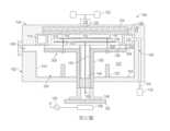
第1A圖及第1B圖為化學氣相沉積(CVD)腔室100的概要剖面視圖,具有接地路徑系統200佈置於其中。腔室100的一個範例為藉由位於美國加州聖克拉拉市的應用材料公司所製造的PRECISION™腔室。腔室100具有腔室主體102及腔室蓋104。腔室主體包括處理空間106及抽吸路徑108。處理空間106為藉由腔室主體及腔室蓋104所界定的空間,且抽吸路徑108為腔室主體102中所形成的路徑,耦接至抽吸板114中所形成的抽吸空間112。1A and 1B are schematic cross-sectional views of a chemical vapor deposition (CVD)
腔室100包括通過腔室蓋104佈置的氣體分配組件116,以遞送一或更多氣體流至此處詳細說明的處理區域110。氣體分配組件116包括氣體歧管118,耦接至腔室蓋104中所形成的氣體入口通道120。氣體歧管118從一或更多氣源122接收氣體流。氣體流分佈橫跨氣箱124,流動通過背板126的複數個孔洞(未顯示),且進一步分佈橫跨藉由背板126及面板130所界定的氣室128。氣體流接著通過面板130的複數個孔洞132流至處理空間106的處理區域110中。幫浦133藉由導管134連接至抽吸路徑108,以控制處理區域110之中的壓力,且通過抽吸空間112及抽吸路徑108從處理區域110排空氣體及副產物。The
處理空間106包括底座138,用於在腔室100之中支撐基板136。底座138包括佈置於其中的加熱元件(未顯示)及電極140。在可與此處所述的其他實施例結合的一個實施例中,電極140包括導電網,例如含有鎢、銅或鉬的導電網。底座138藉由耦接至加熱器夾具144的桿142可移動地佈置於處理空間106中。加熱器夾具144耦接至冷卻樞紐146。冷卻樞紐146連接至舉升系統162,而在抬升處理位置(顯示於第1A圖中)及降低位置(顯示於第1B圖中)之間移動底座138。底座138的移動促進基板136的傳送通過狹縫閥148進出處理空間106,狹縫閥148通過腔室主體102形成。抬升處理位置相對應至藉由氣體分配組件116的底座138及面板130所界定的處理區域110。底座138具有通過其佈置的孔洞,通過此等孔洞可移動地佈置複數個舉升銷150。在降低位置中,複數個舉升銷150藉由接觸耦接至腔室主體的底部154的舉升板152而從底座138突出。舉升銷150的突出將基板136放置於與底座相隔開的關係,以促進基板136的傳送。The
RF源156通過RF匹配電路158耦接至佈置於底座138之中的電極140。RF匹配電路158藉由通過冷卻樞紐146及桿142佈置的導電棒160電氣耦接至電極140。透過接地路徑系統200接地的面板130及電極140促進電容電漿耦合的形成。RF源156提供RF能量至底座138,以促進在氣體分配組件116的底座138及面板130之間亦稱為主要電漿的電容耦合電漿的產生。當供應RF功率至電極140時,在面板130及底座138之間產生電場,使得存在於處理區域110中介於底座138及面板130之間的氣體原子離子化,且釋放電子。離子化的原子加速至底座138,以促進在基板136上形成膜。
接地路徑系統200提供短且對稱的路徑,用於將RF能量從面板130傳播至RF匹配電路158,以減少寄生電漿的產生,且因此增加沉積率且改善膜均勻性。接地路徑系統200包括接地杯體202及底部杯體204。接地杯體202藉由熱屏障228耦接至桿142及底座138。熱屏障228提供對可能被加熱至大於約700°C溫度的底座138的屏障。熱屏障228包括具有低的熱傳導性的材料。在可與此處所述的其他實施例結合的一個實施例中,熱屏障228包括含有鉻鎳鐵合金(inconel)、石英、氧化鋁、氮化鋁及不銹鋼材料之一或更多者,以提供對溫度的屏障。The
接地杯體202亦耦接至冷卻樞紐146,冷卻樞紐146連接至舉升系統162。舉升系統162在抬升處理位置(顯示於第1A圖中)及降低位置(顯示於第1B圖中)之間移動接地杯體202,促進基板136的傳送。接地杯體202包括導電材料,而能夠忍受在處理空間106中大於約700°C的溫度及在處理空間106中的處理環境。在可與此處所述的其他實施例結合的一個實施例中,接地杯體202包括含有鉻鎳鐵合金、鋁及不銹鋼的材料之一或更多者。底部杯體204耦接至底部杯體載具206。底部杯體載具206耦接至軌道208。底部杯體載具206致動以沿著軌道208線性移動,而在接地位置(顯示於第1A圖中)及傳送位置(顯示於第1B圖中)之間移動底部杯體204。軌道208亦可為導軌或纜線。底部杯體載具206包括導電材料,而能夠忍受在處理空間106中的溫度及處理環境。在可與此處所述的其他實施例結合的一個實施例中,底部杯體204包括含有鉻鎳鐵合金、鋁及不銹鋼的材料之一或更多者。
接地杯體202透過接地杯體導體210耦接至底部杯體204。當底座138及接地杯體202在抬升處理位置中時,接地杯體導體在膨脹的狀態,且當底座138及接地杯體202在降低位置中時,接地杯體導體在壓縮的狀態。在膨脹的狀態中的接地杯體導體210提供RF能量傳播的路徑。接地杯體導體210包括導電材料,而能夠忍受處理空間106中的溫度及處理環境。在可與此處所述的其他實施例結合的一個實施例中,接地杯體導體210包括含有基於鎳的合金(例如,HAYNES®230®合金)、鉻鎳鐵合金及不銹鋼材料之一或更多者。在可與此處所述的其他實施例結合的另一實施例中,接地杯體導體210包括複數個風箱212,而在膨脹的狀態中膨脹且在壓縮的狀態中壓縮。The
底部杯體204透過底部杯體導體214耦接至腔室主體102的底部154。當底部杯體204在接地位置中時,底部杯體204在膨脹的狀態,且當底部杯體204在傳送位置中時,底部杯體204在壓縮的狀態。在膨脹的狀態中的底部杯體導體214提供RF能量傳播的路徑。底部杯體導體214包括導電材料,而能夠忍受處理空間106中的溫度及處理環境。在可與此處所述的其他實施例結合的一個實施例中,接地杯體導體210包括含有基於鎳的合金(例如,HAYNES®230®合金)、鉻鎳鐵合金及不銹鋼材料之一或更多者。在可與此處所述的其他實施例結合的另一實施例中,底部杯體導體214包括複數個風箱216,而在膨脹的狀態中膨脹且在壓縮的狀態中壓縮。冷卻樞紐146藉由複數個風箱222耦接至底部杯體載具206,以維持處理空間106之中的壓力。The
在降低位置中的接地杯體202及在傳送位置中的底部杯體204(顯示於第1B圖中)促進基板136的傳送,通過狹縫閥148進出處理空間106,狹縫閥148通過腔室主體102而形成。在抬升處理位置中的接地杯體202及在接地位置中的底部杯體204(顯示於第1A圖中)將處理空間106分叉,以形成處理空間106的內部空間218,而將處理區域110與處理空間106的外部空間220隔絕開。將處理空間106的外部空間220與內部空間218隔絕開對RF能量的傳播提供了減少的表面積,且消除腔室主體102的非對稱性,例如消除藉由狹縫閥148的存在所造成者,而可能造成寄生電漿的形成。The
再者,在接地位置中的底部杯體204接觸抽吸板114,以完成主要RF框架224,用於將RF能量從面板130傳播至RF匹配電路158。在內部空間218中,RF能量沿著主要RF框架224傳播,從面板130至抽吸板114,從底部杯體204至接地杯體導體210,從接地杯體導體210至接地杯體202,且從接地杯體202至導電棒160。藉由在接地位置中的底部杯體204接觸抽吸板114形成的主要RF框架224利用減小的表面積,以賦予更短且更受控的接地路徑,使得在內部空間218中底座138的下方不產生寄生電漿。因此,增加了電容耦合電漿的濃度,且因此增加了電容耦合電漿的密度,而增加膜的沉積率。再者,主要RF框架224實質上為對稱的,以改善電容耦合電漿的均勻性,而改善沉積的膜的均勻性。Again, the
此外,若在接地位置中的底部杯體204並未接觸抽吸板114,則在接地位置中的底部杯體204在外部空間220中形成次要RF框架226。次要RF框架提供RF能量的圍堵。在外部空間220中,RF能量沿著次要RF框架226傳播,從腔室主體102至底部杯體導體214,從底部杯體導體214至底部杯體204,且從底部杯體204至主要RF框架224。Furthermore, the
第1C圖及第1D圖為CVD腔室100的概要剖面視圖,具有接地路徑系統300佈置於其中。透過接地路徑系統300及電極140接地的面板130促進電容電漿耦合的形成。接地路徑系統300提供短且對稱的路徑,用於將射頻(RF)能量從面板130傳播至RF匹配電路158,以減少寄生電漿的產生,且因此增加沉積率且改善膜均勻性。1C and 1D are schematic cross-sectional views of a
接地路徑系統300包括接地杯體302。接地杯體302耦接至冷卻樞紐146。冷卻樞紐146連接至舉升系統162,而在抬升處理位置(顯示於第1C圖中)及降低位置(顯示於第1D圖中)之間移動接地杯體302,促進基板136的傳送。接地杯體302與底座138分開。接地杯體302包括導電材料,而能夠忍受在處理空間106中大於約700°C的溫度且能夠忍受在處理空間106中的處理環境。在可與此處所述的其他實施例結合的一個實施例中,接地杯體302為包括含有鉻鎳鐵合金、鋁及不銹鋼的材料的一或更多者。The
接地杯體302耦接至接地杯體導體304。當底座138及接地杯體302在抬升處理位置中時,接地杯體導體304在壓縮的狀態,且當底座138及接地杯體302在降低位置中時,接地杯體導體在膨脹的狀態。在壓縮的狀態中的接地杯體導體304提供RF能量傳播的路徑。接地杯體導體304包括導電材料,而能夠忍受處理空間106中的溫度。在一個實施例中,接地杯體導體304包括含有基於鎳的合金(例如,HAYNES®230®合金)、鉻鎳鐵合金及不銹鋼材料之一或更多者。在可與此處所述的其他實施例結合的另一實施例中,接地杯體導體304包括複數個風箱306,而在膨脹的狀態中膨脹且在壓縮的狀態中壓縮。The
在降低位置中的接地杯體304(顯示於第1D圖中)促進基板136的傳送,通過狹縫閥148進出處理空間106,狹縫閥148通過腔室主體102而形成。在抬升處理位置中的接地杯體304(顯示於第1C圖中)將處理空間106分叉,以形成處理空間106的內部空間308,而將處理區域110與處理空間106的外部空間310隔絕開。將處理空間106的外部空間310與內部空間308隔絕開對RF能量的傳播提供了減少的表面積,且消除腔室主體102的非對稱性,例如消除藉由狹縫閥148的存在所造成者。腔室主體102的非對稱性可能造成寄生電漿的形成。Grounded cup 304 (shown in FIG. 1D ) in a lowered position facilitates transfer of
再者,當底座138及接地杯體302在抬升處理位置中時,在壓縮的狀態中的接地杯體導體304接觸抽吸板114以完成主要RF框架312,用於從面板130傳播RF能量至RF匹配電路158。在內部空間308中,RF能量沿著主要RF框架312傳播,從面板130至接地杯體導體304,從接地杯體導體304至接地杯體302,且從接地杯體302至導電棒160。藉由在抬升處理位置中的接地杯體302接觸抽吸板114形成的主要RF框架312利用減小的表面積,以賦予更短且更受控的接地路徑,使得在內部空間308中底座138的下方不產生寄生電漿。因此,增加了電容耦合電漿的濃度,且因此增加了電容耦合電漿的密度,而增加膜的沉積率。再者,主要RF框架312實質上為對稱的,以改善電容耦合電漿的均勻性,而改善沉積的膜的均勻性。Again, when
此外,若接地杯體302(在接地位置中)並未接觸抽吸板114,則在抬升處理位置中的接地杯體302在外部空間310中形成次要RF框架314。次要RF框架提供RF能量的圍堵。在外部空間310中,RF能量沿著次要RF框架314傳播,從腔室主體102至接地杯體302,且從接地杯體302至主要RF框架312。Furthermore, the grounded
綜上所述,此處說明的接地路徑系統提供較短且對稱的路徑,用於將RF能量傳播至接地,以減少寄生電漿的產生,且因此增加沉積率且改善膜均勻性。將CVD腔室的處理空間分叉以形成內部空間,而將處理區域與處理空間的外部空間隔絕開,對RF能量的傳播提供了減少的表面積,且消除腔室主體的非對稱性。再者,利用減少的表面積形成主要RF框架賦予更短且更受控的接地路徑,使得在內部空間中底座的下方不產生寄生電漿。因此,增加了電容耦合電漿的濃度,且因此增加了電容耦合電漿的密度,而增加膜的沉積率。再者,主要RF框架實質上為對稱的,以改善電容耦合電漿的均勻性,而改善沉積的膜的均勻性。In summary, the ground path system described here provides a shorter and symmetrical path for propagating RF energy to ground to reduce parasitic plasma generation and thus increase deposition rate and improve film uniformity. Bifurcating the process volume of the CVD chamber to form the interior volume while isolating the process region from the exterior of the process volume provides reduced surface area for the propagation of RF energy and eliminates chamber body asymmetry. Furthermore, forming the primary RF frame with reduced surface area allows for a shorter and more controlled ground path so that no parasitic plasma is generated under the base in the interior space. Thus, the concentration of the capacitively coupled plasma is increased, and thus the density of the capacitively coupled plasma is increased, increasing the deposition rate of the film. Furthermore, the main RF frame is symmetrical in nature to improve the uniformity of the capacitively coupled plasma, which in turn improves the uniformity of the deposited film.
儘管此處所述之態樣關於CVD腔室及其電漿強化的配置,應考量其他處理腔室可從本揭露案的態樣受益。舉例而言,電漿處理腔室可從此處所述的態樣受益,包括電漿處理腔室,例如物理氣相沉積(PVD)腔室、蝕刻腔室、原子層沉積(ALD)腔室,例如電漿強化的ALD腔室等等。Although the aspects described herein relate to the configuration of a CVD chamber and its plasma enhancement, it should be considered that other processing chambers may benefit from aspects of the present disclosure. For example, plasma processing chambers that can benefit from aspects described herein include plasma processing chambers such as physical vapor deposition (PVD) chambers, etch chambers, atomic layer deposition (ALD) chambers, Such as plasma enhanced ALD chamber and so on.
儘管以上導向本揭露案之範例,可衍生本揭露案的其他及進一步範例而不會悖離其基本範疇,且本揭露案之範疇藉由以下申請專利範圍決定。Notwithstanding the above examples leading to this disclosure, other and further examples of this disclosure can be derived without departing from its basic scope, and the scope of this disclosure is determined by the following claims.
100:腔室102:腔室主體104:腔室蓋106:處理空間108:抽吸路徑110:處理區域112:抽吸空間114:抽吸板116:氣體分配組件118:氣體歧管120:氣體入口通道122:氣源124:氣箱126:背板128:氣室130:面板132:孔洞133:幫浦134:導管136:基板138:底座140:電極142:桿144:加熱器夾具146:冷卻樞紐148:狹縫閥150:舉升銷152:舉升板154:底部156:RF源158:RF匹配電路160:導電棒162:舉升系統200:接地路徑系統202:接地杯體204:底部杯體206:底部杯體載具208:軌道210:接地杯體導體212:風箱214:底部杯體導體216:風箱218:內部空間220:外部空間222:風箱224:主要RF框架226:次要RF框架228:熱屏障300:接地路徑系統302:接地杯體304:接地杯體導體306:風箱308:內部空間310:外部空間312:主要RF框架314:次要RF框架100: chamber102: Chamber body104: chamber cover106: Processing space108: Suction path110: Processing area112: suction space114: Suction plate116: Gas distribution components118: Gas manifold120: gas inlet channel122: gas source124: air box126: Backplane128: air chamber130: panel132: hole133: pump134: Conduit136: Substrate138: base140: electrode142: Rod144: heater fixture146: Cooling hub148: Slit valve150:Lift pin152: Lifting plate154: bottom156: RF source158:RF matching circuit160: conductive rod162: Lifting system200: Ground path system202: ground cup204: Bottom cup body206: Bottom cup carrier208: track210: grounding cup conductor212: Bellows214: bottom cup body conductor216: Bellows218: Internal space220: Outer space222: Bellows224: Main RF frame226: Secondary RF frame228: heat barrier300: Ground Path System302: ground cup304: grounding cup conductor306: Bellows308: inner space310: Outer space312: Main RF framework314: Secondary RF frame
由以上方式可詳細理解本揭露案所記載之特徵,以上簡要概述的本揭露案的更具體說明將可藉由參考實施例而獲得,某些實施例圖示於隨附圖式中。然而,應理解隨附圖式僅圖示範例實施例,且因此不應考量為範疇之限制,因為本揭露案認可其他均等效果的實施例。Having thus obtained a detailed understanding of the features recited in the disclosure, a more particular description of the disclosure, briefly summarized above, will be obtained by reference to the Examples, some of which are illustrated in the accompanying drawings. It is to be understood, however, that the accompanying drawings illustrate example embodiments only and are therefore not to be considered limiting of scope, for the present disclosure admits to other equally effective embodiments.
第1A圖為化學氣相沉積腔室的概要剖面視圖,具有根據一實施例的接地路徑系統佈置於其中。Figure 1A is a schematic cross-sectional view of a chemical vapor deposition chamber with a ground path system disposed therein according to an embodiment.
第1B圖為化學氣相沉積腔室的概要剖面視圖,具有根據一實施例的接地路徑系統佈置於其中。FIG. 1B is a schematic cross-sectional view of a chemical vapor deposition chamber with a ground path system disposed therein according to an embodiment.
第1C圖為化學氣相沉積腔室的概要剖面視圖,具有根據一實施例的接地路徑系統佈置於其中。Figure 1C is a schematic cross-sectional view of a chemical vapor deposition chamber with a ground path system disposed therein according to an embodiment.
第1D圖為化學氣相沉積腔室的概要剖面視圖,具有根據一實施例的接地路徑系統佈置於其中。Figure ID is a schematic cross-sectional view of a chemical vapor deposition chamber with a ground path system disposed therein according to an embodiment.
為了促進理解,已儘可能地使用相同的元件符號代表共通圖式中相同的元件。應考量一個實施例的元件及特徵可有益地併入其他實施例中而無須進一步說明。To facilitate understanding, the same reference numerals have been used wherever possible to refer to the same elements in common drawings. It is contemplated that elements and features of one embodiment may be beneficially incorporated in other embodiments without further recitation.
國內寄存資訊 (請依寄存機構、日期、號碼順序註記)無Domestic deposit information (please note in order of depositor, date, and number)none
國外寄存資訊 (請依寄存國家、機構、日期、號碼順序註記)無Overseas storage information (please note in order of storage country, organization, date, and number)none
100:腔室100: chamber
102:腔室主體102: Chamber body
104:腔室蓋104: chamber cover
106:處理空間106: Processing space
108:抽吸路徑108: Suction path
110:處理區域110: Processing area
112:抽吸空間112: suction space
114:抽吸板114: Suction plate
116:氣體分配組件116: Gas distribution components
118:氣體歧管118: Gas manifold
120:氣體入口通道120: gas inlet channel
122:氣源122: gas source
124:氣箱124: air box
126:背板126: Backplane
128:氣室128: air chamber
130:面板130: panel
132:孔洞132: hole
133:幫浦133: pump
134:導管134: Conduit
136:基板136: Substrate
138:底座138: base
140:電極140: electrode
142:桿142: Rod
144:加熱器夾具144: heater fixture
146:冷卻樞紐146: Cooling Hub
148:狹縫閥148: Slit valve
150:舉升銷150:Lift pin
152:舉升板152: Lifting plate
154:底部154: bottom
156:RF源156: RF source
158:RF匹配電路158:RF matching circuit
160:導電棒160: conductive rod
162:舉升系統162: Lifting system
200:接地路徑系統200: Ground path system
202:接地杯體202: ground cup
204:底部杯體204: Bottom cup body
206:底部杯體載具206: Bottom cup carrier
208:軌道208: track
210:接地杯體導體210: grounding cup conductor
212:風箱212: Bellows
214:底部杯體導體214: bottom cup body conductor
216:風箱216: Bellows
218:內部空間218: Internal space
220:外部空間220: Outer space
222:風箱222: Bellows
224:主要RF框架224: Main RF frame
226:次要RF框架226: Secondary RF frame
228:熱屏障228: heat barrier
Claims (20)
Translated fromChineseApplications Claiming Priority (2)
| Application Number | Priority Date | Filing Date | Title |
|---|---|---|---|
| US201862676891P | 2018-05-25 | 2018-05-25 | |
| US62/676,891 | 2018-05-25 |
Publications (2)
| Publication Number | Publication Date |
|---|---|
| TW202012688A TW202012688A (en) | 2020-04-01 |
| TWI798443Btrue TWI798443B (en) | 2023-04-11 |
Family
ID=68615270
Family Applications (2)
| Application Number | Title | Priority Date | Filing Date |
|---|---|---|---|
| TW112109521ATWI832723B (en) | 2018-05-25 | 2019-05-23 | Ground path systems for providing a shorter and symmetrical ground path |
| TW108117843ATWI798443B (en) | 2018-05-25 | 2019-05-23 | Ground path systems for providing a shorter and symmetrical ground path |
Family Applications Before (1)
| Application Number | Title | Priority Date | Filing Date |
|---|---|---|---|
| TW112109521ATWI832723B (en) | 2018-05-25 | 2019-05-23 | Ground path systems for providing a shorter and symmetrical ground path |
Country Status (7)
| Country | Link |
|---|---|
| US (2) | US11434569B2 (en) |
| JP (2) | JP7362669B2 (en) |
| KR (2) | KR20240159024A (en) |
| CN (2) | CN112088426B (en) |
| SG (1) | SG11202009022RA (en) |
| TW (2) | TWI832723B (en) |
| WO (1) | WO2019226294A1 (en) |
Families Citing this family (29)
| Publication number | Priority date | Publication date | Assignee | Title |
|---|---|---|---|---|
| US10224224B2 (en) | 2017-03-10 | 2019-03-05 | Micromaterials, LLC | High pressure wafer processing systems and related methods |
| CN206573826U (en)* | 2017-03-23 | 2017-10-20 | 惠科股份有限公司 | Jacking device and alignment ultraviolet irradiation machine |
| US10622214B2 (en) | 2017-05-25 | 2020-04-14 | Applied Materials, Inc. | Tungsten defluorination by high pressure treatment |
| WO2019036157A1 (en) | 2017-08-18 | 2019-02-21 | Applied Materials, Inc. | High pressure and high temperature anneal chamber |
| US10276411B2 (en) | 2017-08-18 | 2019-04-30 | Applied Materials, Inc. | High pressure and high temperature anneal chamber |
| JP7274461B2 (en) | 2017-09-12 | 2023-05-16 | アプライド マテリアルズ インコーポレイテッド | Apparatus and method for manufacturing semiconductor structures using protective barrier layers |
| CN117936420A (en) | 2017-11-11 | 2024-04-26 | 微材料有限责任公司 | Gas delivery system for high pressure processing chamber |
| JP7330181B2 (en) | 2017-11-16 | 2023-08-21 | アプライド マテリアルズ インコーポレイテッド | High-pressure steam annealing treatment equipment |
| KR20200075892A (en) | 2017-11-17 | 2020-06-26 | 어플라이드 머티어리얼스, 인코포레이티드 | Condenser system for high pressure treatment systems |
| SG11202008256WA (en) | 2018-03-09 | 2020-09-29 | Applied Materials Inc | High pressure annealing process for metal containing materials |
| US10950429B2 (en) | 2018-05-08 | 2021-03-16 | Applied Materials, Inc. | Methods of forming amorphous carbon hard mask layers and hard mask layers formed therefrom |
| US10748783B2 (en) | 2018-07-25 | 2020-08-18 | Applied Materials, Inc. | Gas delivery module |
| US10675581B2 (en) | 2018-08-06 | 2020-06-09 | Applied Materials, Inc. | Gas abatement apparatus |
| CN117305815A (en)* | 2018-09-28 | 2023-12-29 | 应用材料公司 | Coaxial lift with dynamic leveling |
| WO2020117462A1 (en) | 2018-12-07 | 2020-06-11 | Applied Materials, Inc. | Semiconductor processing system |
| US11901222B2 (en) | 2020-02-17 | 2024-02-13 | Applied Materials, Inc. | Multi-step process for flowable gap-fill film |
| US12354847B2 (en)* | 2020-03-12 | 2025-07-08 | Applied Materials, Inc. | Methods and apparatus for conductance liners in semiconductor process chambers |
| US12020957B2 (en)* | 2020-08-31 | 2024-06-25 | Applied Materials, Inc. | Heater assembly with process gap control for batch processing chambers |
| US11887884B2 (en)* | 2020-10-16 | 2024-01-30 | Applied Materials, Inc. | Pre-loaded bowl mechanism for providing a symmetric radio frequency return path |
| US11664247B2 (en) | 2020-10-16 | 2023-05-30 | Applied Materials, Inc. | Dynamic interface for providing a symmetric radio frequency return path |
| KR20240004936A (en)* | 2021-05-07 | 2024-01-11 | 어플라이드 머티어리얼스, 인코포레이티드 | Devices for improved high-pressure plasma processing |
| FI130020B (en)* | 2021-05-10 | 2022-12-30 | Picosun Oy | Substrate processing apparatus and method |
| FI130021B (en)* | 2021-05-10 | 2022-12-30 | Picosun Oy | Substrate processing apparatus and method |
| US20230069317A1 (en)* | 2021-08-25 | 2023-03-02 | Applied Materials, Inc. | Thermal choke plate |
| US20230095095A1 (en)* | 2021-09-27 | 2023-03-30 | Applied Materials, Inc. | Method of isolating the chamber volume to process volume with internal wafer transfer capability |
| CN114023620B (en)* | 2021-10-29 | 2023-07-14 | 德鸿半导体设备(浙江)有限公司 | Processing station for processing substrates |
| WO2023099038A1 (en) | 2021-12-05 | 2023-06-08 | Eaton Intelligent Power Limited | Electrical connector system including a male terminal having a contact arm with a folded portion |
| CN115692263B (en)* | 2022-10-31 | 2023-06-16 | 北京北方华创微电子装备有限公司 | Semiconductor process chamber and semiconductor process equipment |
| US20250118577A1 (en)* | 2023-10-10 | 2025-04-10 | Applied Materials, Inc. | Ceramic rf return kit design |
Citations (6)
| Publication number | Priority date | Publication date | Assignee | Title |
|---|---|---|---|---|
| US5951776A (en)* | 1996-10-25 | 1999-09-14 | Applied Materials, Inc. | Self aligning lift mechanism |
| US20040182515A1 (en)* | 2003-03-19 | 2004-09-23 | Tokyo Electron Limited | Plasma processing apparatus |
| TW201003778A (en)* | 2008-07-03 | 2010-01-16 | Jusung Eng Co Ltd | Dry etching apparatus |
| JP2010161316A (en)* | 2009-01-09 | 2010-07-22 | Ulvac Japan Ltd | Plasma processing device |
| CN102324367A (en)* | 2004-09-21 | 2012-01-18 | 应用材料公司 | RF Grounding of Cathodes in Process Chambers |
| TW201207975A (en)* | 2010-05-12 | 2012-02-16 | Applied Materials Inc | Confined process volume PECVD chamber |
Family Cites Families (21)
| Publication number | Priority date | Publication date | Assignee | Title |
|---|---|---|---|---|
| JPH1079350A (en) | 1996-09-04 | 1998-03-24 | Kokusai Electric Co Ltd | Plasma processing equipment |
| JP4152802B2 (en)* | 2003-05-09 | 2008-09-17 | 日本エー・エス・エム株式会社 | Thin film forming equipment |
| US20070116872A1 (en)* | 2005-11-18 | 2007-05-24 | Tokyo Electron Limited | Apparatus for thermal and plasma enhanced vapor deposition and method of operating |
| US7740705B2 (en)* | 2006-03-08 | 2010-06-22 | Tokyo Electron Limited | Exhaust apparatus configured to reduce particle contamination in a deposition system |
| WO2009104732A1 (en)* | 2008-02-20 | 2009-08-27 | 東京エレクトロン株式会社 | Gas supply device |
| US20100000684A1 (en) | 2008-07-03 | 2010-01-07 | Jong Yong Choi | Dry etching apparatus |
| JP4983885B2 (en)* | 2009-10-16 | 2012-07-25 | 東京エレクトロン株式会社 | Liquid processing apparatus, liquid processing method, and storage medium |
| JP5123329B2 (en)* | 2010-01-07 | 2013-01-23 | 株式会社岡本工作機械製作所 | Semiconductor substrate planarization processing apparatus and planarization processing method |
| US8485128B2 (en)* | 2010-06-30 | 2013-07-16 | Lam Research Corporation | Movable ground ring for a plasma processing chamber |
| US10586686B2 (en)* | 2011-11-22 | 2020-03-10 | Law Research Corporation | Peripheral RF feed and symmetric RF return for symmetric RF delivery |
| US9267739B2 (en)* | 2012-07-18 | 2016-02-23 | Applied Materials, Inc. | Pedestal with multi-zone temperature control and multiple purge capabilities |
| JP6056403B2 (en)* | 2012-11-15 | 2017-01-11 | 東京エレクトロン株式会社 | Deposition equipment |
| US20140273498A1 (en)* | 2013-03-15 | 2014-09-18 | Dainippon Screen Mfg. Co., Ltd. | Substrate processing apparatus and substrate processing method |
| US9620377B2 (en)* | 2014-12-04 | 2017-04-11 | Lab Research Corporation | Technique to deposit metal-containing sidewall passivation for high aspect ratio cylinder etch |
| KR20160083715A (en) | 2015-01-02 | 2016-07-12 | 삼성전자주식회사 | Semiconductor processing apparatus having a gas spray unit |
| US9963782B2 (en) | 2015-02-12 | 2018-05-08 | Asm Ip Holding B.V. | Semiconductor manufacturing apparatus |
| US10049862B2 (en) | 2015-04-17 | 2018-08-14 | Lam Research Corporation | Chamber with vertical support stem for symmetric conductance and RF delivery |
| JP6333232B2 (en) | 2015-12-02 | 2018-05-30 | 株式会社日立国際電気 | Substrate processing apparatus, semiconductor device manufacturing method, and program |
| US20170178758A1 (en)* | 2015-12-18 | 2017-06-22 | Applied Materials, Inc. | Uniform wafer temperature achievement in unsymmetric chamber environment |
| JP6763274B2 (en)* | 2016-10-14 | 2020-09-30 | 東京エレクトロン株式会社 | Film forming equipment, cleaning method of film forming equipment and storage medium |
| JP6698001B2 (en)* | 2016-10-24 | 2020-05-27 | 東京エレクトロン株式会社 | Processing device and cover member |
- 2019
- 2019-05-01USUS16/400,054patent/US11434569B2/enactiveActive
- 2019-05-03JPJP2020565777Apatent/JP7362669B2/enactiveActive
- 2019-05-03KRKR1020247035876Apatent/KR20240159024A/enactivePending
- 2019-05-03SGSG11202009022RApatent/SG11202009022RA/enunknown
- 2019-05-03WOPCT/US2019/030733patent/WO2019226294A1/ennot_activeCeased
- 2019-05-03CNCN201980030846.0Apatent/CN112088426B/enactiveActive
- 2019-05-03KRKR1020207035734Apatent/KR102725261B1/enactiveActive
- 2019-05-03CNCN202411193850.8Apatent/CN119082711A/enactivePending
- 2019-05-23TWTW112109521Apatent/TWI832723B/enactive
- 2019-05-23TWTW108117843Apatent/TWI798443B/enactive
- 2022
- 2022-08-22USUS17/893,018patent/US20220403520A1/enactivePending
- 2023
- 2023-07-18JPJP2023116487Apatent/JP7542117B2/enactiveActive
Patent Citations (6)
| Publication number | Priority date | Publication date | Assignee | Title |
|---|---|---|---|---|
| US5951776A (en)* | 1996-10-25 | 1999-09-14 | Applied Materials, Inc. | Self aligning lift mechanism |
| US20040182515A1 (en)* | 2003-03-19 | 2004-09-23 | Tokyo Electron Limited | Plasma processing apparatus |
| CN102324367A (en)* | 2004-09-21 | 2012-01-18 | 应用材料公司 | RF Grounding of Cathodes in Process Chambers |
| TW201003778A (en)* | 2008-07-03 | 2010-01-16 | Jusung Eng Co Ltd | Dry etching apparatus |
| JP2010161316A (en)* | 2009-01-09 | 2010-07-22 | Ulvac Japan Ltd | Plasma processing device |
| TW201207975A (en)* | 2010-05-12 | 2012-02-16 | Applied Materials Inc | Confined process volume PECVD chamber |
Also Published As
| Publication number | Publication date |
|---|---|
| US20220403520A1 (en) | 2022-12-22 |
| KR20240159024A (en) | 2024-11-05 |
| TWI832723B (en) | 2024-02-11 |
| US20190360100A1 (en) | 2019-11-28 |
| JP7362669B2 (en) | 2023-10-17 |
| CN112088426B (en) | 2024-09-03 |
| KR20210002108A (en) | 2021-01-06 |
| CN112088426A (en) | 2020-12-15 |
| KR102725261B1 (en) | 2024-10-31 |
| WO2019226294A1 (en) | 2019-11-28 |
| TW202012688A (en) | 2020-04-01 |
| TW202332798A (en) | 2023-08-16 |
| SG11202009022RA (en) | 2020-12-30 |
| CN119082711A (en) | 2024-12-06 |
| JP2023156298A (en) | 2023-10-24 |
| JP7542117B2 (en) | 2024-08-29 |
| JP2021525952A (en) | 2021-09-27 |
| US11434569B2 (en) | 2022-09-06 |
Similar Documents
| Publication | Publication Date | Title |
|---|---|---|
| TWI798443B (en) | Ground path systems for providing a shorter and symmetrical ground path | |
| CN110998783B (en) | Substrate support with dual embedded electrodes | |
| CN100385620C (en) | Electrode assembly | |
| US6173673B1 (en) | Method and apparatus for insulating a high power RF electrode through which plasma discharge gases are injected into a processing chamber | |
| TWI407530B (en) | Electrostatic chuck and apparatus for treating substrate including the same | |
| TW202025217A (en) | Semiconductor substrate supports with embedded rf shield | |
| EP3591690B1 (en) | Substrate supporting unit and film forming device having substrate supporting unit | |
| TWI797339B (en) | Apparatus for suppressing parasitic plasma in plasma enhanced chemical vapor deposition chamber | |
| JP2010525612A (en) | Annular baffle | |
| TWI811331B (en) | Microwave plasma source with split window | |
| WO2021132010A1 (en) | Film forming method and film forming system | |
| CN100477091C (en) | processing device | |
| US12170186B2 (en) | Showerhead assembly with heated showerhead | |
| JP2523070B2 (en) | Plasma processing device | |
| JPH10298786A (en) | Surface treatment equipment | |
| US20250316455A1 (en) | Plasma showerhead assembly | |
| US20240068096A1 (en) | Showerhead Assembly with Heated Showerhead | |
| US20250022694A1 (en) | Heater plates with distributed purge channels, rf meshes and ground electrodes | |
| JP2008251838A (en) | Plasma processing equipment | |
| TW202449948A (en) | High temperature biasable heater with advanced far edge electrode, electrostatic chuck, and embedded ground electrode |