TWI796348B - An error amplifier and a pulse width modulation circuit - Google Patents
An error amplifier and a pulse width modulation circuitDownload PDFInfo
- Publication number
- TWI796348B TWI796348BTW107127466ATW107127466ATWI796348BTW I796348 BTWI796348 BTW I796348BTW 107127466 ATW107127466 ATW 107127466ATW 107127466 ATW107127466 ATW 107127466ATW I796348 BTWI796348 BTW I796348B
- Authority
- TW
- Taiwan
- Prior art keywords
- feedback
- signal
- error amplifier
- resistor
- amplifier
- Prior art date
Links
- 239000003990capacitorSubstances0.000claimsabstractdescription60
- 230000010363phase shiftEffects0.000claimsdescription10
- 230000005236sound signalEffects0.000description16
- 230000014509gene expressionEffects0.000description8
- 230000001419dependent effectEffects0.000description3
- 230000005669field effectEffects0.000description3
- 238000005070samplingMethods0.000description3
- 238000010586diagramMethods0.000description2
- 230000001681protective effectEffects0.000description2
- 230000015556catabolic processEffects0.000description1
- 230000003750conditioning effectEffects0.000description1
- 238000006731degradation reactionMethods0.000description1
- 230000009977dual effectEffects0.000description1
- 230000000694effectsEffects0.000description1
- 238000011156evaluationMethods0.000description1
- 238000001914filtrationMethods0.000description1
- 238000005457optimizationMethods0.000description1
- 230000010355oscillationEffects0.000description1
- 238000011045prefiltrationMethods0.000description1
- 238000007493shaping processMethods0.000description1
Images


Classifications
- H—ELECTRICITY
- H03—ELECTRONIC CIRCUITRY
- H03F—AMPLIFIERS
- H03F3/00—Amplifiers with only discharge tubes or only semiconductor devices as amplifying elements
- H03F3/20—Power amplifiers, e.g. Class B amplifiers, Class C amplifiers
- H03F3/21—Power amplifiers, e.g. Class B amplifiers, Class C amplifiers with semiconductor devices only
- H03F3/217—Class D power amplifiers; Switching amplifiers
- H03F3/2171—Class D power amplifiers; Switching amplifiers with field-effect devices
- H—ELECTRICITY
- H03—ELECTRONIC CIRCUITRY
- H03F—AMPLIFIERS
- H03F3/00—Amplifiers with only discharge tubes or only semiconductor devices as amplifying elements
- H03F3/20—Power amplifiers, e.g. Class B amplifiers, Class C amplifiers
- H03F3/21—Power amplifiers, e.g. Class B amplifiers, Class C amplifiers with semiconductor devices only
- H03F3/217—Class D power amplifiers; Switching amplifiers
- H—ELECTRICITY
- H03—ELECTRONIC CIRCUITRY
- H03F—AMPLIFIERS
- H03F1/00—Details of amplifiers with only discharge tubes, only semiconductor devices or only unspecified devices as amplifying elements
- H03F1/32—Modifications of amplifiers to reduce non-linear distortion
- H03F1/3241—Modifications of amplifiers to reduce non-linear distortion using predistortion circuits
- H03F1/3247—Modifications of amplifiers to reduce non-linear distortion using predistortion circuits using feedback acting on predistortion circuits
- H—ELECTRICITY
- H03—ELECTRONIC CIRCUITRY
- H03F—AMPLIFIERS
- H03F1/00—Details of amplifiers with only discharge tubes, only semiconductor devices or only unspecified devices as amplifying elements
- H03F1/32—Modifications of amplifiers to reduce non-linear distortion
- H03F1/3241—Modifications of amplifiers to reduce non-linear distortion using predistortion circuits
- H03F1/3264—Modifications of amplifiers to reduce non-linear distortion using predistortion circuits in audio amplifiers
- H—ELECTRICITY
- H03—ELECTRONIC CIRCUITRY
- H03F—AMPLIFIERS
- H03F1/00—Details of amplifiers with only discharge tubes, only semiconductor devices or only unspecified devices as amplifying elements
- H03F1/32—Modifications of amplifiers to reduce non-linear distortion
- H03F1/3241—Modifications of amplifiers to reduce non-linear distortion using predistortion circuits
- H03F1/3282—Acting on the phase and the amplitude of the input signal
- H—ELECTRICITY
- H03—ELECTRONIC CIRCUITRY
- H03F—AMPLIFIERS
- H03F1/00—Details of amplifiers with only discharge tubes, only semiconductor devices or only unspecified devices as amplifying elements
- H03F1/34—Negative-feedback-circuit arrangements with or without positive feedback
- H—ELECTRICITY
- H03—ELECTRONIC CIRCUITRY
- H03H—IMPEDANCE NETWORKS, e.g. RESONANT CIRCUITS; RESONATORS
- H03H11/00—Networks using active elements
- H03H11/02—Multiple-port networks
- H03H11/04—Frequency selective two-port networks
- H03H11/12—Frequency selective two-port networks using amplifiers with feedback
- H03H11/1204—Distributed RC filters
- H—ELECTRICITY
- H03—ELECTRONIC CIRCUITRY
- H03H—IMPEDANCE NETWORKS, e.g. RESONANT CIRCUITS; RESONATORS
- H03H11/00—Networks using active elements
- H03H11/02—Multiple-port networks
- H03H11/04—Frequency selective two-port networks
- H03H11/12—Frequency selective two-port networks using amplifiers with feedback
- H03H11/126—Frequency selective two-port networks using amplifiers with feedback using a single operational amplifier
- H03H11/1278—Modifications to reduce detrimental influences of amplifier imperfections, e.g. limited gain-bandwith product, limited input impedance
- H—ELECTRICITY
- H03—ELECTRONIC CIRCUITRY
- H03F—AMPLIFIERS
- H03F2200/00—Indexing scheme relating to amplifiers
- H03F2200/03—Indexing scheme relating to amplifiers the amplifier being designed for audio applications
- H—ELECTRICITY
- H03—ELECTRONIC CIRCUITRY
- H03F—AMPLIFIERS
- H03F2200/00—Indexing scheme relating to amplifiers
- H03F2200/135—Indexing scheme relating to amplifiers there being a feedback over one or more internal stages in the global amplifier
- H—ELECTRICITY
- H03—ELECTRONIC CIRCUITRY
- H03F—AMPLIFIERS
- H03F2200/00—Indexing scheme relating to amplifiers
- H03F2200/144—Indexing scheme relating to amplifiers the feedback circuit of the amplifier stage comprising a passive resistor and passive capacitor
Landscapes
- Engineering & Computer Science (AREA)
- Power Engineering (AREA)
- Physics & Mathematics (AREA)
- Nonlinear Science (AREA)
- Multimedia (AREA)
- Amplifiers (AREA)
Abstract
Description
Translated fromChinese本發明係有關於一種誤差放大器。具體地,本發明係有關於一種用於脈波寬度調變電路之誤差放大器及一種包括該誤差放大器之脈波寬度調變電路。The present invention relates to an error amplifier. Specifically, the present invention relates to an error amplifier for a pulse width modulation circuit and a pulse width modulation circuit including the error amplifier.
第1圖說明音頻脈波寬度調變(PWM)放大器2之實例。音頻PWM放大器係一種切換放大器,其切換頻率超過音頻信號的最高音頻頻率之2倍且在音頻信號的最高音頻頻率之20至40倍的範圍內。放大器2包括誤差放大器,其配置成將放大器的切換輸出與音頻輸入信號進行比較,以確保輸出係輸入信號的線性比例版本且補償因有限且變動負載配置及匯流排電壓的變化所造成之匯流排輸出電壓相對於輸入信號的變化。在所述圖式中,誤差放大器配置成包括運算放大器(op-amp)4,運算放大器與前饋電容器6構造成一個積分器。運算放大器4在其反相輸入處經由輸入電阻器8接收音頻信號,並且經由反饋電阻器10接收來自放大器的切換級之輸出信號。運算放大器4的音頻信號輸出耦合至比較器12,比較器12將音頻信號輸出與由信號發生器14產生的三角形或鋸齒形調變波形組合。FIG. 1 illustrates an example of an audio pulse width modulated (PWM)
放大器包括功率級16。功率級16包括閘極驅動器或切換控制器18,其輸出包含具有變動寬度及間隔之固定振幅的方形脈波之信號。可以理解的是,閘極驅動器18產生由保護延遲或控檔時間(protective delay or dead time)隔開之一個信號以及這個信號的位準移位且反相版。閘極驅動器18接收來自比較器12之調變信號。接收的調變信號之低頻部分係要放大的音頻信號,而高頻部分係三角形或鋸齒形波形,三角形或鋸齒形波形用於在與低頻音頻信號組合時產生數位信號(亦即,在兩個不同的預定匯流排電壓之間切換的信號)。The amplifier includes a
功率級16包括兩個切換裝置20、22。閘極驅動器18的輸出以推挽(push-pull)或圖騰柱(totem-pole)配置耦合至這兩個切換裝置。在第1圖所示的電路中,開係係場效電晶體(FET)20、22。在這個圖式中,上FET22由驅動器18輸出的信號來驅動,而下FET 20由這個信號的位準移位且反相版來驅動。兩個開關20、22配置成完全導通或完全斷開,使得切換裝置的輸出處於+Vcc或-Vcc(亦即,匯流排電壓)。這種類型的配置利用這樣的特性:如果推挽輸出裝置完全導通或完全斷開,則它們消耗其最小功率,從而導致高的放大器效率。如上所述,功率級16的輸出(亦即,來自放大器的切換級之輸出)被反饋至誤差放大器。The
使用被動式濾波器24對功率級16的輸出進行低通濾波,以濾除切換頻率,以允許放大器2的揚聲器負載30僅看到音頻信號。用於被動式濾波器24的標準且常用濾波器係雙極點電感器-電容器(LC)濾波器。被動式濾波器24的常用組件值係20μH的串聯電感器26及分流至接地之470nF的電容器28。The output of the
關於圖1所述的實例係一個音頻實例,但是可以理解的是,誤差放大器可以與其他應用(例如,旋轉或扭矩產生電動機及發光二極體)結合來使用。The example described with respect to Figure 1 is an audio example, but it is understood that the error amplifier can be used in conjunction with other applications such as rotary or torque generating motors and light emitting diodes.
由於邏輯閘的時序及溫度相關的電路電容,PWM功率輸出級的信號路徑可能造成過量的相移。這是因為電容值係與溫度相關的,並且相移亦可能與溫度相關的,這可能導致誤差放大器不穩定、信號退化及電路損壞的可能性。對於要使用的整體負反饋(global negative feedback),誤差放大器實際上應該對在切換頻率及其諧波下的過量相移具有彈性。The signal path of the PWM power output stage can cause excessive phase shift due to logic gate timing and temperature-dependent circuit capacitance. This is because the capacitance value is temperature dependent, and the phase shift may also be temperature dependent, which can lead to error amplifier instability, signal degradation and the possibility of circuit damage. For global negative feedback to be used, the error amplifier should actually be resilient to excessive phase shifts at the switching frequency and its harmonics.
這些考慮因素通常基於多重反饋、Sallen-Key或狀態變數拓撲濾波器分成單獨的區塊(blocks)。然而,增加的區塊數會增加電路複雜性,這本身可能導致過量的相移及降低的性能。當減少電路區塊時,應該考慮運算放大器及所使用高頻的選擇,因為在誤差放大器電路中需要顯著的增益帶寬乘積(GBP),以避免不受控制的行為(例如,在電源軌處的輸出鎖定、振盪、因沒有提供預期的濾波功能而沒有切換頻率的拒斥、比運算放大器部分所規定還高的信號失真)。These considerations are usually divided into separate blocks based on multiple feedback, Sallen-Key or state variable topology filters. However, the increased number of blocks increases circuit complexity, which itself can lead to excessive phase shift and reduced performance. When reducing circuit blocks, the choice of op amp and the high frequencies used should be considered, since a significant gain-bandwidth product (GBP) is required in the error amplifier circuit to avoid uncontrolled behavior (e.g., output locking, oscillations, rejection of switching frequency because it does not provide expected filtering, signal distortion higher than specified in the op amp section).
因此,需要考量上述考慮因素來提供一種簡化誤差放大器。Therefore, there is a need to provide a simplified error amplifier that takes into account the above considerations.
依據本發明的第一實施例,提供一種用於脈波寬度調變電路之誤差放大器,該誤差放大器包括一運算放大器,其構造成一積分器;以及一反饋迴路,其耦合於該運算放大器之信號輸出與該運算放大器之反相輸入之間,該反饋迴路包括一耦合至該信號輸出之反饋電容器、一耦合至該反饋電容器之反饋電阻器以及一耦合至該反饋電阻器及該運算放大器之反相輸入的積分器電阻器,其中該反饋電阻器與該積分器電阻器之間的接點係構造成接收一輸入信號,而該反饋電容器與該反饋電阻器之間的接點係構造成從該脈波寬度調變電路接收一反饋信號。因此,誤差放大器具有在不使用多電路區塊的情況下考慮上述設計要求之單級電路。According to a first embodiment of the present invention, an error amplifier for a pulse width modulation circuit is provided, the error amplifier includes an operational amplifier configured as an integrator; and a feedback loop coupled to the operational amplifier Between the signal output and the inverting input of the operational amplifier, the feedback loop includes a feedback capacitor coupled to the signal output, a feedback resistor coupled to the feedback capacitor, and a feedback resistor coupled to the feedback resistor and the operational amplifier. Inverting input integrator resistor, wherein the junction between the feedback resistor and the integrator resistor is configured to receive an input signal, and the junction between the feedback capacitor and the feedback resistor is configured to A feedback signal is received from the PWM circuit. Therefore, the error amplifier has a single-stage circuit that takes into account the above-mentioned design requirements without using multiple circuit blocks.
該反饋電容器可以配置成補償在切換頻率下的過量相移。The feedback capacitor can be configured to compensate for excess phase shift at the switching frequency.
該積分器電阻器配置成將該誤差放大器的積分功能與反饋求和功能分開。The integrator resistor is configured to separate the integrating function of the error amplifier from the feedback summing function.
該誤差放大器可以包括一第一低通濾波器,該第一低通濾波器耦合至該反饋電容器與該反饋電阻器之間的接點,並且配置成從該脈波寬度調變電路接收該反饋信號,其中該第一低通濾波器構造成衰減該反饋信號的調變分量。The error amplifier may include a first low pass filter coupled to the junction between the feedback capacitor and the feedback resistor and configured to receive the a feedback signal, wherein the first low-pass filter is configured to attenuate a modulation component of the feedback signal.
該誤差放大器可以包括一第二低通濾波器,該第二低通濾波器耦合至該反饋電阻器與該積分器電阻器之間的接點,並且配置成接收該輸入信號,其中該第二低通濾波器係構造成衰減該輸入信號的混疊頻率分量。The error amplifier may include a second low pass filter coupled to the junction between the feedback resistor and the integrator resistor and configured to receive the input signal, wherein the firstTwo low pass filters are configured to attenuate aliased frequency components of the input signal.
該誤差放大器可以包括一並聯電容器,該並聯電容器配置在該誤差放大器的信號輸入處,藉此與該第二低通濾波器構成一pi輸入濾波器,其中該pi輸入濾波器構造成防止來自該反饋信號的切換能量被傳導至一信號驅動分量。The error amplifier may include a shunt capacitor arranged at the signal input of the error amplifier thereby forming a pi input filter with the second low pass filter, wherein the pi input filter is configured to prevent The switching energy of the feedback signal is conducted to a signal driving component.
該積分器可以包括一耦合於該運算放大器的信號輸出與反相輸入之間的前饋電容器。The integrator may include a feedforward capacitor coupled between the signal output and the inverting input of the operational amplifier.
依據本發明的第二實施例,提供一種脈波寬度調變電路,該脈波寬度調變電路包括一驅動電路,其構造成輸出一調變信號;一切換裝置,其配置成從該驅動電路接收該調變信號;以及依據該第一實施例之誤差放大器,其具有上述任選特徵中之一個以上的特徵。該切換裝置的輸出信號係該反饋信號,並且其中該運算放大器的信號輸出耦合至該驅動電路。According to the second embodiment of the present invention, there is provided a pulse width modulation circuit, the pulse width modulation circuit includes a driving circuit configured to output a modulation signal; a switching device configured to output from the The driving circuit receives the modulation signal; and the error amplifier according to the first embodiment has at least one of the above optional features. The output signal of the switching device is the feedback signal, and wherein the signal output of the operational amplifier is coupled to the driving circuit.
該脈波寬度調變電路可以包括以推挽式配置來構造之兩個切換裝置。The pulse width modulation circuit may include two switching devices configured in a push-pull configuration.
該脈波寬度調變電路可以耦合至一揚聲器或一電動機。The PWM circuit can be coupled to a speaker or a motor.
一種設計成用於PWM放大器的誤差放大器通常包括求和以及一積分器或一前饋路徑濾波器,並且可以任選地包括一反饋路徑濾波器。當設計誤差放大器電路級時,應該考慮幾個要求,這將在下面作論述。An error amplifier designed for use with a PWM amplifier typically includes summing and an integrator or a feedforward path filter, and may optionally include a feedback path filter. When designing the error amplifier circuit stage, several requirements should be considered, which will be discussed below.
一種用於PWM放大器的誤差放大器通常以一運算放大器、積體或離散電路為基礎,該電路應該包括適當高的「增益×帶寬」乘積,以線性地操作直至最大感興趣頻率(例如,400kHz或音頻信號的最高音頻、切換頻率及其諧波的20至40倍高)。該誤差放大器應該在音頻信號頻率範圍內具有高性能,因為該誤差放大器將界定PWM電路之信號品質的極限。再者,該誤差放大器的電源軌應該與PWM電路電壓切換位準相匹配或包括信號調節,以確保低壓軌運算放大器在其輸入端看不到超過其電源軌的電壓,因為這會導致運算放大器的破壞及降低電路的可靠性。An error amplifier for a PWM amplifier usually starts withBased on an operational amplifier, integrated or discrete circuit, the circuit should include a suitably high "gain x bandwidth" product to operate linearly up to the maximum frequency of interest (e.g., 400kHz or the highest frequency of the audio signal, the switching frequency and its 20 to 40 times higher than the harmonics). The error amplifier should have high performance in the frequency range of the audio signal, because the error amplifier will define the limit of the signal quality of the PWM circuit. Again, the supply rail for this error amplifier should match the PWM circuit voltage switching level or include signal conditioning to ensure that the low-rail op amp does not see a voltage at its input that exceeds its supply rail, as this would cause the op amp's damage and reduce the reliability of the circuit.
一個預調節電路區塊構造成為從調變信號的反饋比例版本濾除或衰減匯流排電壓位準PWM電路取樣頻率。輸出電壓軌至軌切換位準可能超過信號位準電壓的電源及誤差放大器級的電源。一個用於輸入音頻信號的預濾波電路區塊確保饋入至PWM電路的輸入音頻信號不包含例如超過PWM電路之取樣(亦即,切換)頻率的一半之混疊頻率分量。這是因為超過PWM電路之取樣(亦即,切換)頻率的一半之頻率將被有效地引回至輸入信號中,導致信號失真,並且因帶內折返(in-band foldback)而不可能被移除。A pre-regulator circuit block is configured to filter or attenuate the bus voltage level PWM circuit sampling frequency from a feedback proportional version of the modulated signal. Power supplies for which output voltage rail-to-rail switching levels may exceed the signal level voltage and power supplies for the error amplifier stage. A pre-filter circuit block for the input audio signal ensures that the input audio signal fed to the PWM circuit does not contain aliased frequency components, for example exceeding half the sampling (ie, switching) frequency of the PWM circuit. This is because frequencies above half the sampling (ie, switching) frequency of the PWM circuit will effectively be introduced back into the input signal, distorting the signal and impossible to remove due to in-band foldback .
該電路的PWM高壓切換閘極驅動器18及輸出功率切換裝置20、22插在該誤差放大器的輸出與反饋之間,以允許高功率輸送至輸出負載(例如,揚聲器30)。The circuit's PWM high voltage
如在典型的反饋控制電路之情況中,在該誤差放大器內需要求和操作,以便能夠使用負反饋,因為負反饋降低非線性且亦降低輸出阻抗。對於低PWM放大器輸出失真,可以應用整體負反饋,以允許該誤差放大器校正PWM功率輸出級的輸出之任何非線性。As in the case of typical feedback control circuits, a summing operation is required within the error amplifier in order to be able to use negative feedback becauseNegative feedback reduces nonlinearity and also reduces output impedance. For low PWM amplifier output distortion, integral negative feedback can be applied to allow the error amplifier to correct any non-linearity in the output of the PWM power output stage.
下面呈現的誤差放大器構造成考慮上述所有的要求。下面描述的誤差放大器電路已設計成為適用於PWM切換放大器的新型專業級濾波器,其結合上述設計考慮因素成單級電路。這種配置使用單個運算放大器級來提供改善的電路性能。再者,當使電阻值最佳化時,這個配置針對施加至誤差放大器端子的過電壓條件提供固有的可靠性。The error amplifier presented below is constructed to take into account all of the above requirements. The error amplifier circuit described below has been designed as a new professional-grade filter for PWM switching amplifiers incorporating the above design considerations into a single-stage circuit. This configuration uses a single op amp stage to provide improved circuit performance. Again, when the resistor values are optimized, this configuration provides inherent reliability against overvoltage conditions applied to the error amplifier terminals.
2‧‧‧音頻脈波寬度調變(PWM)放大器2‧‧‧Audio pulse width modulation (PWM) amplifier
4‧‧‧運算放大器4‧‧‧Operational Amplifier
6‧‧‧前饋電容器6‧‧‧Feedforward capacitor
8‧‧‧輸入電阻器8‧‧‧Input Resistor
10‧‧‧反饋電阻器10‧‧‧Feedback Resistor
12‧‧‧比較器12‧‧‧Comparator
14‧‧‧信號發生器14‧‧‧Signal generator
16‧‧‧功率級16‧‧‧power level
18‧‧‧閘極驅動器或切換控制器18‧‧‧Gate driver or switching controller
20‧‧‧切換裝置20‧‧‧Switching device
22‧‧‧切換裝置22‧‧‧Switching device
24‧‧‧被動式濾波器24‧‧‧passive filter
26‧‧‧串聯電感器26‧‧‧Series inductor
28‧‧‧電容器28‧‧‧Capacitor
30‧‧‧揚聲器負載30‧‧‧Speaker load
40‧‧‧誤差放大器40‧‧‧Error Amplifier
42‧‧‧端子或接點42‧‧‧terminal or contact
44‧‧‧端子或接點44‧‧‧terminal or contact
46‧‧‧端子或接點46‧‧‧terminal or contact
48‧‧‧端子或接點48‧‧‧terminal or contact
50‧‧‧運算放大器50‧‧‧operational amplifier
52‧‧‧前饋電容器52‧‧‧Feedforward capacitor
54‧‧‧反饋電容器54‧‧‧Feedback capacitor
56‧‧‧第一反饋電阻器56‧‧‧First feedback resistor
58‧‧‧積分器電阻器58‧‧‧Integrator resistor
60‧‧‧輸入電阻器60‧‧‧input resistor
62‧‧‧第三反饋電阻器62‧‧‧The third feedback resistor
64‧‧‧低通電容器64‧‧‧Low-pass capacitor
66‧‧‧第二反饋電阻器66‧‧‧Second feedback resistor
70‧‧‧誤差放大器70‧‧‧Error Amplifier
72‧‧‧第一並聯電容器72‧‧‧First parallel capacitor
74‧‧‧第二並聯電容器74‧‧‧Second parallel capacitor
76‧‧‧第二串聯電阻器76‧‧‧Second series resistor
80‧‧‧音頻脈波寬度調變(PWM)放大器80‧‧‧Audio Pulse Width Modulation (PWM) Amplifier
82‧‧‧誤差放大器82‧‧‧Error Amplifier
100‧‧‧DC或AC電動機控制電路100‧‧‧DC or AC motor control circuit
102‧‧‧誤差放大器102‧‧‧Error Amplifier
104‧‧‧功率級104‧‧‧power level
106‧‧‧閘極驅動器或切換控制器106‧‧‧Gate driver or switching controller
108‧‧‧切換裝置108‧‧‧Switching device
110‧‧‧切換裝置110‧‧‧switching device
112‧‧‧被動式濾波器112‧‧‧Passive filter
114‧‧‧串聯電感器114‧‧‧Series inductor
116‧‧‧電容器116‧‧‧Capacitor
118‧‧‧電動機118‧‧‧Motor
120‧‧‧替代DC或AC電動機控制電路120‧‧‧Replacing DC or AC motor control circuit
122‧‧‧誤差放大器122‧‧‧Error Amplifier
124‧‧‧閘極驅動器或切換控制器124‧‧‧Gate driver or switching controller
126‧‧‧開關126‧‧‧Switch
128‧‧‧電動機128‧‧‧Motor
參考下面闡述的實施例之敘述並結合所附圖式可以理解本發明,其中:上面描述的第1圖說明音頻脈波寬度調變(PWM)放大器的一個實例;第2圖說明依據本發明的第一態樣之誤差放大器;第3圖說明依據本發明的第二態樣之誤差放大器;第4圖說明依據本發明的第三態樣之音頻脈波寬度調變(PWM)放大器;第5圖說明依據本發明的第四態樣之DC或AC電動機控制電路;以及第6圖說明依據本發明的第五態樣之DC或AC電動機控制電路。The present invention can be understood by reference to the description of the embodiments set forth below in conjunction with the accompanying drawings, wherein: Figure 1 of the above description illustrates an example of an audio pulse width modulation (PWM) amplifier; First Aspect Error Amplifier; FIG. 3 illustrates an error amplifier according to a second aspect of the invention; FIG. 4 illustrates an audio pulse width modulation (PWM) amplifier according to a third aspect of the invention; FIG. 5 Figure 6 illustrates a DC or AC motor control circuit according to a fourth aspect of the invention; and Figure 6 illustrates a DC or AC motor control circuit according to a fifth aspect of the invention.
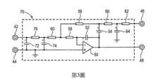
第2圖說明依據本發明的第一態樣之誤差放大器40。放大器40在端子或接點42處接收輸入音頻信號,並且在端子或接點48處產生輸出音頻信號。端子或接點44耦合至接地。端子或接點46耦合至PWM放大器之功率級的輸出。Fig. 2 illustrates the error amplifier according to the first aspect of the
誤差放大器40包括針對期望帶寬及信號失真特性所選擇的運算放大器50,例如,AD8651,其耦合至與PWM放大器(未顯示)的切換級相同之匯流排電壓供應線(亦即,+Vcc及-Vcc)。運算放大器50構造成積分器,其具有耦合於運算放大器50的信號輸出與運算放大器50的反相輸入之間的前饋電容器52,以及積分器電阻器58。放大器亦包括耦合於運算放大器50的信號輸出與運算放大器50的反相輸入之間的反饋迴路。反饋迴路包括耦合至運算放大器50的信號輸出之反饋電容器54、耦合至反饋電容器54的第一反饋電阻器56及積分器電阻器58。積分器電阻器58通常大於或等於100歐姆以及將運算放大器配置的積分功能與運算放大器配置的反饋求和功能分開,並且提供積分器頻率的極點倍增。
音頻信號經由輸入電阻器60饋送至誤差放大器40。輸入電阻器60耦合至積分器電阻器58及第一反饋電阻器56。確切地說,輸入電阻器60耦合至積分器電阻器58與第一反饋電阻器56的/之間的接點或端子。從PMW放大器的切換級經由第二反饋電阻器66來反饋信號。The audio signal is fed to error
低通濾波器配置在誤差放大器的反饋輸入46處。低通濾波器包括第三反饋電阻器62及分流至接地的低通電容器64。通常在FSwitching/10的範圍中將低通電容器64調諧至電路的-3dB頻率,以允許迴路減少來最小化混疊。A low pass filter is arranged at the
可以根據下面表達式來選擇低通電容器64:CLow-pass capacitor 64=1/(2π*RThird feedback resistor 62*F)The low-
其中F係電路的-3dB頻率。Among them, the -3dB frequency of the F series circuit.
低通電容器64具有雙重功能,除了提供迴路增益減少之外,這種電容器還提供開迴路零點(open-loop zero),以允許由放大器的PWM功率輸出級輸出的切換信號之相移校正。應該進行設計評估,以按優先順序處理在低通電容器64充當可給出20dB的拒斥之切換頻率濾波器來預調節反饋信號中存在的切換頻率與對提供給誤差放大器輸入端的反饋信號之相位校正貢獻之間的功能。從針對-3dB頻率=fs/10所計算出的數值增加電容器64的數值,因而增加反饋信號的相位超前。
使用下面表達式來決定誤差放大器40的增益:AV=-((RFirst feedback resistor 56+RSecond feedback resistor 66+RThird feedback resistor 62)/RInput resister 60)。The gain of the
根據下面表達式來選擇前饋或積分器電容器52:CFeed forwardcapacitor52=1/(((AV*RIntegratorresistor 58)+RFirst feedback resistor 56+RSecond feedback resistor 66+RThird feedbackresistor 62)*2π*FIntegrator)The feed forward or
其中FIntegrator=FSwitching/ax。對於具有20kHz的最大頻率及400kHz的切換頻率(FSwitching)之音頻應用,ax=3π提供最佳的濾波器塑形(shape)及滾降(roll off)。whereFIntegrator =FSwitching/ax . For audio applications with a maximum frequency of 20kHz and a switching frequency (FSwitching ) of 400kHz, ax =3π provides the best filter shape and roll off.
添加反饋電容器54,以對在切換頻率及其倍數處的任何過量相移提供局部補償。這可以改善穩定性且降低可能由放大器的PWM功率輸出級引起的相移影響。反饋電容器54有效地在誤差放大器的閉迴路頻率響應中添加極點及零點。A
下面表達式可用於根據一個期望極點位置的頻率來決定反饋電容器54的電容值:CFeedback capacitor54=1/(2π*(RSecond feedback resistor 66+RThird feedback resistor 62)*FPole)The following expression can be used to determine the capacitance value of the
其中FPole=FSwitcking/bx。whereFPole =FSwitching/bx .
下面表達式可用於決定由反饋電容器54的電容值提供的零頻率:FZero=1/(2π*RFirst feedback resistor 56*CFeedback capacitor54)。The following expression can be used to determine the zero frequency provided by the capacitance of the feedback capacitor 54:FZero =1/(2π *RFirst feedback resistor 56 *CFeedback capacitor54) .
誤差放大器在切換頻率處的增益應該較佳地限制在大約6dB。對於具有20kHz的最大頻率及400kHz的切換頻率(FSwitching)之音頻應用,bx=2π提供最佳濾波器塑形及滾降。在不影響信號頻率範圍內的線性之情況下,反饋電容器54降低在切換頻率下誤差放大器電路之「增益×帶寬」乘積的要求。The gain of the error amplifier should preferably be limited to about 6dB at the switching frequency. For audio applications with a maximum frequency of 20kHz and a switching frequency (FSwitching ) of 400kHz, bx =2π provides the best filter shaping and roll-off.
上面論述的表達式提供i)在切換頻率處大於20dB的增益減少,以及ii)在20kHz處具有最小相移的平坦通帶響應達到20kHz(亦即,音頻在信號頻率範圍的上限)。根據應用,誤差放大器之組件值的最佳化可以提供期望的誤差放大器增益及相位特性。The expressions discussed above provide i) greater than 20dB of gain reduction at the switching frequency, and ii) a flat passband response with minimal phase shift at 20kHz up to 20kHz (i.e.upper limit). Depending on the application, optimization of error amplifier component values can provide desired error amplifier gain and phase characteristics.
在一個實例中,選擇10.4的增益(AV),並且選擇下面組件值:RInput resister 60=1,000R;RIntegrator resistor 58=100R;RFirst feedback resistor 56=1,000R;RSecond feedback resistor 66=4,700R;RThird feedback resistor 62=4,700R;FSwitching=400,000Hz。In one example, a gain (AV) of 10.4 is selected, and the following component values are selected:RInput resistor 60 =1,000R;RIntegrator resistor 58 =100R;RFirst feedback resistor 56 =1,000R;RSecond feedback resistor 66 =4,700 R;RThird feedback resistor 62 =4,700R;FSwitching =400,000Hz.
根據上面提供的表達式及42,441Hz的積分器頻率(亦即,FIntegrator=400,000/3π),可以決定下面的電容值:CLow-pass capacitor 64=1/(2π*4,700R*400,000Hz)=847pFAccording to the expression provided above and the integrator frequency of 42,441Hz (that is,FIntegrator =400,000/3π), the following capacitor value can be determined:CLow-pass capacitor 64 =1/(2π *4,700R*400,000Hz) =847pF
CFeed forward capacitor 52=1/(((10.4*100R)+1,000R+4,700R+4,700R)*2π*42,441Hz)=327pFCFeed forward capacitor 52 =1/(((10.4*100R)+1,000R+4,700R+4,700R)*2π*42,441Hz)=327pF
CFeedback capacitor 54=1/((4,700R+4,700R)*400,000Hz)=266pF。CFeedback capacitor 54 =1/(( 4,700R+4,700R) *400,000Hz) =266pF.
可以理解的是,將使用接近理論值的電容器。It will be appreciated that capacitors close to theoretical values will be used.
第3圖說明依據本發明的第二態樣之誤差放大器70。在第3圖中使用相同的元件符號來標記第2圖所描述的組件及特徵。第3圖所示的誤差放大器70在其輸入端包括π輸入濾波器。在這個圖式中,π輸入濾波器在端子42處接收音頻輸入信號且耦合至輸入電阻器60。π輸入濾波器包括第一並聯電容器72及第二並聯電容器74,它們由第二串聯電阻器76隔開。π輸入濾波器的添加可以保護PWM放大器免受呈現給誤差放大器輸入的混疊頻率分量之影響。值得注意的是,第3圖中的第二串聯電阻器76及輸入電阻器60之組合等效於第2圖中的單個輸入電阻器60。亦可以包括電感器與端子42串聯或與串聯電阻器76串聯,以改善拒斥。再者,第一並聯電容器72的包含係任選的,使得在其不存在的情況下可以形成低通濾波器。Figure 3 illustrates an
第4圖說明依據本發明的第三態樣之音頻脈波寬度調變(PWM)放大器80。放大器80包括誤差放大器82,其可以是第2圖所描述的誤差放大器40或第3圖所描述的誤差放大器70。第4圖的其他編號組件與第1圖所示的相同編號組件相同。在放大器80中,在端子或接點42處接收輸入音頻信號,並且端子或接點48經由比較器12耦合至閘極驅動器18。開關20、22的輸出耦合至誤差放大器82的端子或接點46。Figure 4 illustrates an audio pulse width modulated (PWM)
第5圖說明依據本發明的第四態樣之DC或AC電動機控制電路100。電路100包括誤差放大器102,其可以是第2圖所描述的誤差放大器40或第3圖所描述的誤差放大器70之形式。誤差放大器40及誤差放大器70中的每一者已經與音頻放大器結合在一起來描述,但是這些放大器的形式可以用作DC或AC電動機控制電路的一部分,並且如何根據那些誤差放大器的一般敘述選擇適當的組件值對於熟悉技藝者來說將是顯而易見的。誤差放大器102的輸出經由比較器12饋送至功率級104,功率級104包括閘極驅動器或切換控制器106,其輸出包含具有變動寬度及間隔的固定振幅之方形脈波的信號。可以理解的是,閘極驅動器106產生由保護延遲或控檔時間(protective delay or dead time)隔開之一個信號以及這個信號的位準移位且反相版。功率級104包括兩個切換裝置108、110(例如,場效電晶體(FET))。兩個開關108、110配置成完全導通或完全斷開,使得切換裝置的輸出處於+Vcc或-Vcc(亦即,匯流排電壓)。這種類型的配置利用這樣的特性:如果推挽輸出裝置完全導通或完全斷開,則它們消耗其最小功率,從而導致高的放大器效率。如上面關於音頻放大器所述,功率級104的輸出被反饋至誤差放大器102。Fig. 5 illustrates a DC or AC
使用被動式濾波器112對功率級104的輸出進行低通濾波,以濾除切換頻率,然後將其饋送至電動機118。被動式濾波器112係雙極點電感器-電容器(LC)濾波器,其包括串聯電感器114及分流至接地的電容器116。串聯電感器114及並聯電容器116的組件值可以使用表達式-F-3dB=1/2π*
第6圖說明依據本發明的第五態樣之替代DC或AC電動機控制電路120。電路120包括誤差放大器122,其係第5圖所描述的誤差放大器102之形式。誤差放大器122的輸出被饋送至閘極驅動器或切換控制器124,閘極驅動器或切換控制器124輸出包含具有變動寬度及間隔的固定振幅之方形脈波的信號。在這個實例中,單個開關126(例如,場效電晶體(FET)與電動機128串聯使用,電動機128配置在電壓電源(亦即,+Vcc或-Vcc)之間,並且控制器124的輸出信號被饋送至開關126的控制輸入(亦即,閘極)。Figure 6 illustrates an alternative DC or AC
可以理解的是,前面的論述係有關於特定實施例。然而,在其他實施例中,可以組合各種態樣及實例。It is to be understood that the foregoing discussion is in relation to specific embodiments. However, in other embodiments, various aspects and examples may be combined.
Claims (8)
Translated fromChineseApplications Claiming Priority (3)
| Application Number | Priority Date | Filing Date | Title |
|---|---|---|---|
| GB1712647.5AGB2565293A (en) | 2017-08-07 | 2017-08-07 | An error amplifier |
| ??GB1712647.5 | 2017-08-07 | ||
| GBGB1712647.5 | 2017-08-07 |
Publications (2)
| Publication Number | Publication Date |
|---|---|
| TW201924213A TW201924213A (en) | 2019-06-16 |
| TWI796348Btrue TWI796348B (en) | 2023-03-21 |
Family
ID=59894774
Family Applications (1)
| Application Number | Title | Priority Date | Filing Date |
|---|---|---|---|
| TW107127466ATWI796348B (en) | 2017-08-07 | 2018-08-07 | An error amplifier and a pulse width modulation circuit |
Country Status (6)
| Country | Link |
|---|---|
| US (1) | US10931242B2 (en) |
| EP (1) | EP3665774A1 (en) |
| JP (1) | JP7227247B2 (en) |
| GB (1) | GB2565293A (en) |
| TW (1) | TWI796348B (en) |
| WO (1) | WO2019030518A1 (en) |
Families Citing this family (4)
| Publication number | Priority date | Publication date | Assignee | Title |
|---|---|---|---|---|
| GB2565293A (en)* | 2017-08-07 | 2019-02-13 | Reid Acoustic Designs Ltd | An error amplifier |
| CN110868162A (en) | 2019-11-29 | 2020-03-06 | 上海艾为电子技术股份有限公司 | A digital audio power amplifier and power amplifier loop |
| US11271480B2 (en)* | 2020-08-03 | 2022-03-08 | xMEMS Labs, Inc. | Driving circuit with energy recycle capability and method thereof |
| US12160206B2 (en)* | 2021-06-16 | 2024-12-03 | Mediatek Inc. | DC-blocking amplifier with aliasing tone cancellation circuit |
Citations (5)
| Publication number | Priority date | Publication date | Assignee | Title |
|---|---|---|---|---|
| US20070188222A1 (en)* | 2004-05-18 | 2007-08-16 | Nphysics, Inc. | Self-oscillating switching amplifier |
| US20070247219A1 (en)* | 2006-04-07 | 2007-10-25 | Jesus Rodriguez Manuel D | Switching power amplifier |
| US20100164449A1 (en)* | 2008-12-29 | 2010-07-01 | Mirmira Ramarao Dwarakanath | Power Converter with a Dynamically Configurable Controller and Output Filter |
| US20140062592A1 (en)* | 2012-08-30 | 2014-03-06 | Anpec Electronics Corporation | Pop-free single-ended output class-d amplifier |
| WO2019030518A1 (en)* | 2017-08-07 | 2019-02-14 | Reid Acoustic Designs Ltd | An error amplifier |
Family Cites Families (17)
| Publication number | Priority date | Publication date | Assignee | Title |
|---|---|---|---|---|
| US4189681A (en)* | 1978-09-29 | 1980-02-19 | Neil Brown Instruments Systems, Inc. | Bandpass filter having low passband phase shift |
| US5635871A (en)* | 1992-12-15 | 1997-06-03 | Doble Engineering Company | Low phase error amplifying |
| US5805020A (en)* | 1996-06-27 | 1998-09-08 | Harris Corporation | Silent start class D amplifier |
| US6529068B1 (en)* | 1997-08-29 | 2003-03-04 | Stmicroelectronics S.R.L. | Area-efficient reconstruction filters, particularly for current-driven D/A converters |
| DE19838765A1 (en)* | 1998-08-26 | 2000-05-11 | Elbo Gmbh | Self-oscillating digital amplifier with delay-free digital negative feedback, without push-pull distortions |
| EP1204207B1 (en)* | 2000-10-14 | 2007-09-26 | Micronas GmbH | Active filter circuit with operational amplifier |
| JP3941443B2 (en) | 2001-09-27 | 2007-07-04 | ヤマハ株式会社 | Self-propelled PWM amplifier |
| JP2005123949A (en)* | 2003-10-17 | 2005-05-12 | Yamaha Corp | Class d amplifier |
| GB2440188B (en)* | 2006-07-14 | 2011-06-08 | Wolfson Ltd | Amplifier Circuits, Methods of Starting and Stopping Amplifier Circuits |
| TWI348815B (en)* | 2008-06-06 | 2011-09-11 | Amazing Microelectronic Corp | Class d amplifier |
| KR20100008749A (en)* | 2008-07-16 | 2010-01-26 | 삼성전자주식회사 | Switching power amplifier and control method thereof |
| JP2010157970A (en)* | 2009-01-05 | 2010-07-15 | Kenwood Corp | Self-excited class-d amplifier |
| JP2012015650A (en) | 2010-06-29 | 2012-01-19 | Renesas Electronics Corp | Class-d amplifier |
| EP2845314B1 (en) | 2012-04-30 | 2016-06-29 | Merus Audio ApS | Class d audio amplifier with adjustable loop filter characteristics |
| US9287826B2 (en)* | 2012-09-04 | 2016-03-15 | Conta Pronat Gmbh | Sine-cosine modulator |
| US9294057B2 (en)* | 2013-12-18 | 2016-03-22 | National Instruments Corporation | Efficient low noise high speed amplifier |
| JP6510199B2 (en) | 2014-08-19 | 2019-05-08 | ローム株式会社 | Switching circuit, audio amplifier integrated circuit, electronic device, driving method of electroacoustic transducer |
- 2017
- 2017-08-07GBGB1712647.5Apatent/GB2565293A/ennot_activeWithdrawn
- 2018
- 2018-08-07JPJP2020529826Apatent/JP7227247B2/enactiveActive
- 2018-08-07WOPCT/GB2018/052254patent/WO2019030518A1/ennot_activeCeased
- 2018-08-07EPEP18769416.1Apatent/EP3665774A1/enactivePending
- 2018-08-07USUS16/637,240patent/US10931242B2/enactiveActive
- 2018-08-07TWTW107127466Apatent/TWI796348B/enactive
Patent Citations (5)
| Publication number | Priority date | Publication date | Assignee | Title |
|---|---|---|---|---|
| US20070188222A1 (en)* | 2004-05-18 | 2007-08-16 | Nphysics, Inc. | Self-oscillating switching amplifier |
| US20070247219A1 (en)* | 2006-04-07 | 2007-10-25 | Jesus Rodriguez Manuel D | Switching power amplifier |
| US20100164449A1 (en)* | 2008-12-29 | 2010-07-01 | Mirmira Ramarao Dwarakanath | Power Converter with a Dynamically Configurable Controller and Output Filter |
| US20140062592A1 (en)* | 2012-08-30 | 2014-03-06 | Anpec Electronics Corporation | Pop-free single-ended output class-d amplifier |
| WO2019030518A1 (en)* | 2017-08-07 | 2019-02-14 | Reid Acoustic Designs Ltd | An error amplifier |
Also Published As
| Publication number | Publication date |
|---|---|
| JP2020530247A (en) | 2020-10-15 |
| WO2019030518A1 (en) | 2019-02-14 |
| GB201712647D0 (en) | 2017-09-20 |
| EP3665774A1 (en) | 2020-06-17 |
| US10931242B2 (en) | 2021-02-23 |
| GB2565293A (en) | 2019-02-13 |
| JP7227247B2 (en) | 2023-02-21 |
| TW201924213A (en) | 2019-06-16 |
| US20200235707A1 (en) | 2020-07-23 |
Similar Documents
| Publication | Publication Date | Title |
|---|---|---|
| TWI796348B (en) | An error amplifier and a pulse width modulation circuit | |
| TWI477064B (en) | A system and method for reducing distortion in an audio amplification system | |
| JP4434557B2 (en) | Power amplifier circuit | |
| US8013677B2 (en) | One-sided switching pulse width modulation amplifiers | |
| US7372324B2 (en) | Digital amplifier | |
| US9806684B2 (en) | Method and apparatus for achieving very high-output signal swing from class-D amplifier | |
| CN101465622B (en) | D-genus audio power amplifier | |
| EP2375566B1 (en) | Duplicate feedback network in class D amplifiers | |
| CN107046404A (en) | Class D amplifier and method for performing class D amplification | |
| US20220263473A1 (en) | Method for controlling a driver circuit, driver circuit, system comprising a driver circuit and method for manufacturing an integrated circuit | |
| EP1530286B1 (en) | Class D amplifier | |
| US10164581B2 (en) | Self-oscillating amplifier with high order loop filter | |
| EP1630954A1 (en) | A feedback circuit | |
| US7675362B2 (en) | Switching amplifier | |
| JP2017175586A (en) | Self-excited class d amplifier of btl output | |
| EP1825592B1 (en) | A power multiplier apparatus and method | |
| JP6699073B2 (en) | Self-excited class D amplifier | |
| WO2014132953A1 (en) | D-class amplifier and electronic apparatus | |
| JP2007209038A (en) | Power amplifier circuit | |
| US20200412320A1 (en) | An electronic filter apparatus | |
| JP2014011763A (en) | Class d amplification circuit and class d amplification method |