TWI792493B - Total internal reflection display - Google Patents
Total internal reflection displayDownload PDFInfo
- Publication number
- TWI792493B TWI792493BTW110130000ATW110130000ATWI792493BTW I792493 BTWI792493 BTW I792493BTW 110130000 ATW110130000 ATW 110130000ATW 110130000 ATW110130000 ATW 110130000ATW I792493 BTWI792493 BTW I792493B
- Authority
- TW
- Taiwan
- Prior art keywords
- layer
- total reflection
- dielectric layer
- reflection display
- sub
- Prior art date
Links
- 239000011159matrix materialSubstances0.000claimsabstractdescription19
- 239000000758substrateSubstances0.000claimsdescription35
- 239000010409thin filmSubstances0.000claimsdescription20
- 239000002245particleSubstances0.000description21
- 230000004888barrier functionEffects0.000description4
- 230000000694effectsEffects0.000description4
- 238000010586diagramMethods0.000description2
- 238000000034methodMethods0.000description2
- 230000003287optical effectEffects0.000description2
- 108091081062Repeated sequence (DNA)Proteins0.000description1
- 230000004075alterationEffects0.000description1
- 238000010276constructionMethods0.000description1
- 239000000463materialSubstances0.000description1
- 230000002093peripheral effectEffects0.000description1
- 230000008569processEffects0.000description1
- 238000000926separation methodMethods0.000description1
- 238000001179sorption measurementMethods0.000description1
- 238000006467substitution reactionMethods0.000description1
Images


Classifications
- G—PHYSICS
- G02—OPTICS
- G02F—OPTICAL DEVICES OR ARRANGEMENTS FOR THE CONTROL OF LIGHT BY MODIFICATION OF THE OPTICAL PROPERTIES OF THE MEDIA OF THE ELEMENTS INVOLVED THEREIN; NON-LINEAR OPTICS; FREQUENCY-CHANGING OF LIGHT; OPTICAL LOGIC ELEMENTS; OPTICAL ANALOGUE/DIGITAL CONVERTERS
- G02F1/00—Devices or arrangements for the control of the intensity, colour, phase, polarisation or direction of light arriving from an independent light source, e.g. switching, gating or modulating; Non-linear optics
- G02F1/01—Devices or arrangements for the control of the intensity, colour, phase, polarisation or direction of light arriving from an independent light source, e.g. switching, gating or modulating; Non-linear optics for the control of the intensity, phase, polarisation or colour
- G02F1/165—Devices or arrangements for the control of the intensity, colour, phase, polarisation or direction of light arriving from an independent light source, e.g. switching, gating or modulating; Non-linear optics for the control of the intensity, phase, polarisation or colour based on translational movement of particles in a fluid under the influence of an applied field
- G02F1/166—Devices or arrangements for the control of the intensity, colour, phase, polarisation or direction of light arriving from an independent light source, e.g. switching, gating or modulating; Non-linear optics for the control of the intensity, phase, polarisation or colour based on translational movement of particles in a fluid under the influence of an applied field characterised by the electro-optical or magneto-optical effect
- G02F1/167—Devices or arrangements for the control of the intensity, colour, phase, polarisation or direction of light arriving from an independent light source, e.g. switching, gating or modulating; Non-linear optics for the control of the intensity, phase, polarisation or colour based on translational movement of particles in a fluid under the influence of an applied field characterised by the electro-optical or magneto-optical effect by electrophoresis
- G—PHYSICS
- G09—EDUCATION; CRYPTOGRAPHY; DISPLAY; ADVERTISING; SEALS
- G09G—ARRANGEMENTS OR CIRCUITS FOR CONTROL OF INDICATING DEVICES USING STATIC MEANS TO PRESENT VARIABLE INFORMATION
- G09G3/00—Control arrangements or circuits, of interest only in connection with visual indicators other than cathode-ray tubes
- G09G3/20—Control arrangements or circuits, of interest only in connection with visual indicators other than cathode-ray tubes for presentation of an assembly of a number of characters, e.g. a page, by composing the assembly by combination of individual elements arranged in a matrix no fixed position being assigned to or needed to be assigned to the individual characters or partial characters
- G09G3/34—Control arrangements or circuits, of interest only in connection with visual indicators other than cathode-ray tubes for presentation of an assembly of a number of characters, e.g. a page, by composing the assembly by combination of individual elements arranged in a matrix no fixed position being assigned to or needed to be assigned to the individual characters or partial characters by control of light from an independent source
- G09G3/3433—Control arrangements or circuits, of interest only in connection with visual indicators other than cathode-ray tubes for presentation of an assembly of a number of characters, e.g. a page, by composing the assembly by combination of individual elements arranged in a matrix no fixed position being assigned to or needed to be assigned to the individual characters or partial characters by control of light from an independent source using light modulating elements actuated by an electric field and being other than liquid crystal devices and electrochromic devices
- G09G3/344—Control arrangements or circuits, of interest only in connection with visual indicators other than cathode-ray tubes for presentation of an assembly of a number of characters, e.g. a page, by composing the assembly by combination of individual elements arranged in a matrix no fixed position being assigned to or needed to be assigned to the individual characters or partial characters by control of light from an independent source using light modulating elements actuated by an electric field and being other than liquid crystal devices and electrochromic devices based on particles moving in a fluid or in a gas, e.g. electrophoretic devices
- G—PHYSICS
- G02—OPTICS
- G02F—OPTICAL DEVICES OR ARRANGEMENTS FOR THE CONTROL OF LIGHT BY MODIFICATION OF THE OPTICAL PROPERTIES OF THE MEDIA OF THE ELEMENTS INVOLVED THEREIN; NON-LINEAR OPTICS; FREQUENCY-CHANGING OF LIGHT; OPTICAL LOGIC ELEMENTS; OPTICAL ANALOGUE/DIGITAL CONVERTERS
- G02F1/00—Devices or arrangements for the control of the intensity, colour, phase, polarisation or direction of light arriving from an independent light source, e.g. switching, gating or modulating; Non-linear optics
- G02F1/01—Devices or arrangements for the control of the intensity, colour, phase, polarisation or direction of light arriving from an independent light source, e.g. switching, gating or modulating; Non-linear optics for the control of the intensity, phase, polarisation or colour
- G02F1/13—Devices or arrangements for the control of the intensity, colour, phase, polarisation or direction of light arriving from an independent light source, e.g. switching, gating or modulating; Non-linear optics for the control of the intensity, phase, polarisation or colour based on liquid crystals, e.g. single liquid crystal display cells
- G02F1/133—Constructional arrangements; Operation of liquid crystal cells; Circuit arrangements
- G02F1/1333—Constructional arrangements; Manufacturing methods
- G02F1/1335—Structural association of cells with optical devices, e.g. polarisers or reflectors
- G02F1/133509—Filters, e.g. light shielding masks
- G02F1/133512—Light shielding layers, e.g. black matrix
- G—PHYSICS
- G02—OPTICS
- G02F—OPTICAL DEVICES OR ARRANGEMENTS FOR THE CONTROL OF LIGHT BY MODIFICATION OF THE OPTICAL PROPERTIES OF THE MEDIA OF THE ELEMENTS INVOLVED THEREIN; NON-LINEAR OPTICS; FREQUENCY-CHANGING OF LIGHT; OPTICAL LOGIC ELEMENTS; OPTICAL ANALOGUE/DIGITAL CONVERTERS
- G02F1/00—Devices or arrangements for the control of the intensity, colour, phase, polarisation or direction of light arriving from an independent light source, e.g. switching, gating or modulating; Non-linear optics
- G02F1/01—Devices or arrangements for the control of the intensity, colour, phase, polarisation or direction of light arriving from an independent light source, e.g. switching, gating or modulating; Non-linear optics for the control of the intensity, phase, polarisation or colour
- G02F1/13—Devices or arrangements for the control of the intensity, colour, phase, polarisation or direction of light arriving from an independent light source, e.g. switching, gating or modulating; Non-linear optics for the control of the intensity, phase, polarisation or colour based on liquid crystals, e.g. single liquid crystal display cells
- G02F1/133—Constructional arrangements; Operation of liquid crystal cells; Circuit arrangements
- G02F1/1333—Constructional arrangements; Manufacturing methods
- G02F1/1335—Structural association of cells with optical devices, e.g. polarisers or reflectors
- G02F1/133509—Filters, e.g. light shielding masks
- G02F1/133514—Colour filters
- G—PHYSICS
- G02—OPTICS
- G02F—OPTICAL DEVICES OR ARRANGEMENTS FOR THE CONTROL OF LIGHT BY MODIFICATION OF THE OPTICAL PROPERTIES OF THE MEDIA OF THE ELEMENTS INVOLVED THEREIN; NON-LINEAR OPTICS; FREQUENCY-CHANGING OF LIGHT; OPTICAL LOGIC ELEMENTS; OPTICAL ANALOGUE/DIGITAL CONVERTERS
- G02F1/00—Devices or arrangements for the control of the intensity, colour, phase, polarisation or direction of light arriving from an independent light source, e.g. switching, gating or modulating; Non-linear optics
- G02F1/01—Devices or arrangements for the control of the intensity, colour, phase, polarisation or direction of light arriving from an independent light source, e.g. switching, gating or modulating; Non-linear optics for the control of the intensity, phase, polarisation or colour
- G02F1/165—Devices or arrangements for the control of the intensity, colour, phase, polarisation or direction of light arriving from an independent light source, e.g. switching, gating or modulating; Non-linear optics for the control of the intensity, phase, polarisation or colour based on translational movement of particles in a fluid under the influence of an applied field
- G02F1/1675—Constructional details
- G02F1/1676—Electrodes
- G02F1/16766—Electrodes for active matrices
- G—PHYSICS
- G02—OPTICS
- G02F—OPTICAL DEVICES OR ARRANGEMENTS FOR THE CONTROL OF LIGHT BY MODIFICATION OF THE OPTICAL PROPERTIES OF THE MEDIA OF THE ELEMENTS INVOLVED THEREIN; NON-LINEAR OPTICS; FREQUENCY-CHANGING OF LIGHT; OPTICAL LOGIC ELEMENTS; OPTICAL ANALOGUE/DIGITAL CONVERTERS
- G02F1/00—Devices or arrangements for the control of the intensity, colour, phase, polarisation or direction of light arriving from an independent light source, e.g. switching, gating or modulating; Non-linear optics
- G02F1/01—Devices or arrangements for the control of the intensity, colour, phase, polarisation or direction of light arriving from an independent light source, e.g. switching, gating or modulating; Non-linear optics for the control of the intensity, phase, polarisation or colour
- G02F1/165—Devices or arrangements for the control of the intensity, colour, phase, polarisation or direction of light arriving from an independent light source, e.g. switching, gating or modulating; Non-linear optics for the control of the intensity, phase, polarisation or colour based on translational movement of particles in a fluid under the influence of an applied field
- G02F1/1675—Constructional details
- G02F1/1677—Structural association of cells with optical devices, e.g. reflectors or illuminating devices
- G—PHYSICS
- G02—OPTICS
- G02F—OPTICAL DEVICES OR ARRANGEMENTS FOR THE CONTROL OF LIGHT BY MODIFICATION OF THE OPTICAL PROPERTIES OF THE MEDIA OF THE ELEMENTS INVOLVED THEREIN; NON-LINEAR OPTICS; FREQUENCY-CHANGING OF LIGHT; OPTICAL LOGIC ELEMENTS; OPTICAL ANALOGUE/DIGITAL CONVERTERS
- G02F1/00—Devices or arrangements for the control of the intensity, colour, phase, polarisation or direction of light arriving from an independent light source, e.g. switching, gating or modulating; Non-linear optics
- G02F1/01—Devices or arrangements for the control of the intensity, colour, phase, polarisation or direction of light arriving from an independent light source, e.g. switching, gating or modulating; Non-linear optics for the control of the intensity, phase, polarisation or colour
- G02F1/19—Devices or arrangements for the control of the intensity, colour, phase, polarisation or direction of light arriving from an independent light source, e.g. switching, gating or modulating; Non-linear optics for the control of the intensity, phase, polarisation or colour based on variable-reflection or variable-refraction elements not provided for in groups G02F1/015 - G02F1/169
- G02F1/195—Devices or arrangements for the control of the intensity, colour, phase, polarisation or direction of light arriving from an independent light source, e.g. switching, gating or modulating; Non-linear optics for the control of the intensity, phase, polarisation or colour based on variable-reflection or variable-refraction elements not provided for in groups G02F1/015 - G02F1/169 by using frustrated reflection
Landscapes
- Physics & Mathematics (AREA)
- Nonlinear Science (AREA)
- General Physics & Mathematics (AREA)
- Optics & Photonics (AREA)
- Chemical & Material Sciences (AREA)
- Engineering & Computer Science (AREA)
- Mathematical Physics (AREA)
- Crystallography & Structural Chemistry (AREA)
- Health & Medical Sciences (AREA)
- Molecular Biology (AREA)
- Electrochemistry (AREA)
- Chemical Kinetics & Catalysis (AREA)
- Life Sciences & Earth Sciences (AREA)
- Computer Hardware Design (AREA)
- Theoretical Computer Science (AREA)
- Electrochromic Elements, Electrophoresis, Or Variable Reflection Or Absorption Elements (AREA)
- Devices For Indicating Variable Information By Combining Individual Elements (AREA)
- Prostheses (AREA)
Abstract
Description
Translated fromChinese本揭露係關於一種全反射顯示器。The present disclosure relates to a total reflection display.
一般而言,全反射顯示器通常具有透鏡層與顯示介電層,並且可藉由透明電極控制顯示介電層中的帶電黑色粒子的移動方向。舉例來說,當透鏡層表面上的透明電極提供正電位時,顯示介電層中的帶電黑色粒子向上移動以吸收光線,可視為全反射顯示器的暗態。當薄膜電晶體基板的透明電極提供正電位時,顯示介電層中的帶電黑色粒子向下移動,使透鏡層反射光線,可視為全反射顯示器的亮態。然而,由於薄膜電晶體基板的透明電極吸附帶電黑色粒子的效果不佳,透鏡層無法反射多數光線,使全反射顯示器的亮態效率低,降低了全反射顯示器的整體表現。Generally speaking, a total reflection display usually has a lens layer and a display dielectric layer, and the movement direction of the charged black particles in the display dielectric layer can be controlled by a transparent electrode. For example, when the transparent electrodes on the surface of the lens layer provide a positive potential, the charged black particles in the display dielectric layer move upwards to absorb light, which can be regarded as the dark state of the total reflection display. When the transparent electrode of the thin film transistor substrate provides a positive potential, the charged black particles in the display dielectric layer move downward, causing the lens layer to reflect light, which can be regarded as the bright state of the total reflection display. However, since the transparent electrode of the thin film transistor substrate is not effective in absorbing charged black particles, the lens layer cannot reflect most of the light, so that the bright state efficiency of the total reflection display is low, and the overall performance of the total reflection display is reduced.
本揭露之一技術態樣為一種全反射顯示器。One technical aspect of the present disclosure is a total reflection display.
根據本揭露一實施方式,一種全反射顯示器包括子畫素、反射層、至少一第一立體電極以及顯示介質層。子畫素由相鄰設置的濾光片與黑色矩陣定義。反射層位於子畫素下方。第一立體電極位於子畫素的黑色矩陣下方。第一立體電極的寬度小於黑色矩陣的寬度。顯示介質層位於子畫素與反射層之間。第一立體電極的高度大於顯示介質層的厚度之半。According to an embodiment of the present disclosure, a total reflection display includes sub-pixels, a reflective layer, at least one first three-dimensional electrode, and a display medium layer. Sub-pixels are defined by adjacently placed filters and black matrices. The reflective layer sits below the sub-pixels. The first three-dimensional electrode is located under the black matrix of the sub-pixel. The width of the first three-dimensional electrode is smaller than the width of the black matrix. The display medium layer is located between the sub-pixels and the reflective layer. The height of the first three-dimensional electrode is greater than half of the thickness of the display medium layer.
在本揭露一實施方式中,上述全反射顯示器更包括第一介電層以及薄膜電晶體基板。第一介電層圍繞第一立體電極。薄膜電晶體基板具有第一透明電極。第一透明電極電性連接第一立體電極。In an embodiment of the present disclosure, the above-mentioned total reflection display further includes a first dielectric layer and a TFT substrate. The first dielectric layer surrounds the first three-dimensional electrode. The thin film transistor substrate has a first transparent electrode. The first transparent electrode is electrically connected to the first three-dimensional electrode.
在本揭露一實施方式中,上述反射層的寬度大致相同於子畫素的濾光片的寬度。In an embodiment of the present disclosure, the width of the reflective layer is substantially the same as the width of the filter of the sub-pixel.
在本揭露一實施方式中,上述反射層位於薄膜電晶體基板上且具有頂面與側壁。反射層的頂面、側壁以及薄膜電晶體基板的頂面定義出階梯狀表面。In an embodiment of the present disclosure, the reflective layer is located on the TFT substrate and has a top surface and sidewalls. The top surface of the reflective layer, the side walls and the top surface of the thin film transistor substrate define a stepped surface.
在本揭露一實施方式中,上述全反射顯示器更包括第一透鏡層、第二透明電極以及第二介電層。第一透鏡層設置於子畫素與顯示介質層之間。第二透明電極位於第一透鏡層與顯示介質層之間。第二介電層位於第二透明電極與顯示介質層之間。In an embodiment of the present disclosure, the above-mentioned total reflection display further includes a first lens layer, a second transparent electrode, and a second dielectric layer. The first lens layer is disposed between the sub-pixels and the display medium layer. The second transparent electrode is located between the first lens layer and the display medium layer. The second dielectric layer is located between the second transparent electrode and the display medium layer.
在本揭露一實施方式中,上述全反射顯示器更包括檔牆以及第二立體電極。檔牆設置於第二介電層與薄膜電晶體基板之間,且位於子畫素外圍。第二立體電極設置於檔牆中。In an embodiment of the present disclosure, the above-mentioned total reflection display further includes a retaining wall and a second three-dimensional electrode. The barrier wall is disposed between the second dielectric layer and the thin film transistor substrate, and is located on the periphery of the sub-pixel. The second three-dimensional electrode is arranged in the retaining wall.
在本揭露一實施方式中,上述第一介電層覆蓋反射層的頂面與側壁。第一介電層與第一透鏡層分開。In an embodiment of the present disclosure, the above-mentioned first dielectric layer covers the top surface and the sidewall of the reflective layer. The first dielectric layer is separated from the first lens layer.
在本揭露一實施方式中,上述全反射顯示器更包括第三介電層。第三介電層覆蓋反射層的頂面與側壁。第一介電層接觸第一透鏡層且與薄膜電晶體基板分開。In an embodiment of the present disclosure, the above-mentioned total reflection display further includes a third dielectric layer. The third dielectric layer covers the top surface and the sidewall of the reflective layer. The first dielectric layer contacts the first lens layer and is separated from the TFT substrate.
在本揭露一實施方式中,上述第一立體電極的寬度在1μm至32μm的範圍中。In an embodiment of the present disclosure, the width of the first three-dimensional electrode is in the range of 1 μm to 32 μm.
在本揭露一實施方式中,上述全反射顯示器更包括第二透鏡層以及第三透明電極。第二透鏡層位於薄膜電晶體基板與反射層之間。第二透鏡層與反射層之間具有空氣間隙。第三透明電極位於子畫素與薄膜電晶體基板之間。In an embodiment of the present disclosure, the above-mentioned total reflection display further includes a second lens layer and a third transparent electrode. The second lens layer is located between the thin film transistor substrate and the reflective layer. There is an air gap between the second lens layer and the reflective layer. The third transparent electrode is located between the sub-pixel and the TFT substrate.
在本揭露一實施方式中,上述反射層的寬度大於第三透明電極的寬度。In an embodiment of the present disclosure, the reflective layer has a width greater than that of the third transparent electrode.
在本揭露一實施方式中,上述第一介電層延伸至第三透明電極上。第三透明電極與子畫素分開。In an embodiment of the present disclosure, the above-mentioned first dielectric layer extends to the third transparent electrode. The third transparent electrode is separated from the sub-pixels.
在本揭露一實施方式中,上述第一介電層延伸至薄膜電晶體基板上。第三透明電極與第一介電層分開。In an embodiment of the present disclosure, the above-mentioned first dielectric layer extends to the TFT substrate. The third transparent electrode is separated from the first dielectric layer.
在本揭露一實施方式中,上述全反射顯示器更包括第四介電層。第四介電層覆蓋第三透明電極。顯示介質層位於第四介電層與第一介電層之間。In an embodiment of the present disclosure, the above-mentioned total reflection display further includes a fourth dielectric layer. The fourth dielectric layer covers the third transparent electrode. The display medium layer is located between the fourth dielectric layer and the first dielectric layer.
在本揭露上述實施方式中,全反射顯示器具有反射層、第一立體電極以及顯示介質層。由於第一立體電極的高度大於顯示介質層的厚度之半,因此當第一立體電極提供正電位時,顯示介質層中的帶電黑色粒子可移動至具有足夠高度的第一立體電極上,可提高第一立體電極吸附帶電黑色粒子的效率,使較多光線可進入反射層中以提高反射效果。此外,可藉由提高第一立體電極的高度以縮小第一立體電極的寬度,使第一立體電極的寬度小於子畫素的黑色矩陣的寬度,以提高全反射顯示器的開口率,進而增加全反射顯示器的亮態反射率。In the above embodiments of the present disclosure, the total reflection display has a reflection layer, a first three-dimensional electrode, and a display medium layer. Because the height of the first three-dimensional electrode is greater than half of the thickness of the display medium layer, when the first three-dimensional electrode provides a positive potential, the charged black particles in the display medium layer can move to the first three-dimensional electrode with sufficient height, which can improve The adsorption efficiency of the charged black particles by the first three-dimensional electrode enables more light to enter the reflective layer to improve the reflective effect. In addition, the width of the first three-dimensional electrode can be reduced by increasing the height of the first three-dimensional electrode, so that the width of the first three-dimensional electrode is smaller than the width of the black matrix of the sub-pixel, so as to increase the aperture ratio of the total reflection display, thereby increasing the overall The bright state reflectance of reflective displays.
以下揭示之實施方式內容提供了用於實施所提供的標的之不同特徵的許多不同實施方式,或實例。下文描述了元件和佈置之特定實例以簡化本案。當然,該等實例僅為實例且並不意欲作為限制。此外,本案可在各個實例中重複元件符號及/或字母。此重複係用於簡便和清晰的目的,且其本身不指定所論述的各個實施方式及/或配置之間的關係。The embodiments disclosed below provide many different implementations, or examples, for implementing different features of the provided subject matter. Specific examples of components and arrangements are described below to simplify the present case. Of course, these examples are only examples and are not intended to be limiting. In addition, the present case may repeat element symbols and/or letters in various instances. This repetition is for the purposes of brevity and clarity and does not in itself dictate a relationship between the various implementations and/or configurations discussed.
諸如「在……下方」、「在……之下」、「下部」、「在……之上」、「上部」等等空間相對術語可在本文中為了便於描述之目的而使用,以描述如附圖中所示之一個元件或特徵與另一元件或特徵之關係。空間相對術語意欲涵蓋除了附圖中所示的定向之外的在使用或製作方法中的裝置的不同定向。裝置可經其他方式定向(旋轉90度或以其他定向)並且本文所使用的空間相對描述詞可同樣相應地解釋。Spatially relative terms such as "below", "beneath", "lower", "above", "upper", etc. may be used herein for convenience of description to describe The relationship of one element or feature to another element or feature as shown in the drawings. Spatially relative terms are intended to encompass different orientations of the device in a method of use or making in addition to the orientation depicted in the figures. The device may be otherwise oriented (rotated 90 degrees or at other orientations) and the spatially relative descriptors used herein interpreted accordingly.
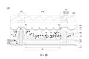
第1圖繪示根據本揭露一實施方式之全反射顯示器100的子畫素190的上視圖。第2圖繪示第1圖沿線2-2之全反射顯示器100的剖面圖。同時參照第1圖與第2圖,全反射顯示器100包括子畫素190、反射層120、至少一第一立體電極140以及顯示介質層150。子畫素190由相鄰設置的濾光片192與黑色矩陣194定義。子畫素190上方可設有前光模組200。反射層120位於子畫素190的濾光片192下方,而第一立體電極140位於子畫素190的黑色矩陣194下方,且第一立體電極140的數量並不以此為限。第一立體電極140的寬度W1小於子畫素190的黑色矩陣194的寬度W2,並且反射層120的寬度W3大致相同於子畫素190的濾光片192的寬度W4。顯示介質層150位於子畫素190與反射層120之間。舉例來說,顯示介質層150中具有低折射率介質與帶電黑色粒子。帶電黑色粒子具有負電特性,可在低折射率介質中移動。並且,第一立體電極140的高度H1大於顯示介質層150的厚度H2之半。FIG. 1 shows a top view of a
在本實施方式中,全反射顯示器100還包括第一介電層130以及薄膜電晶體基板110。第一介電層130位於顯示介質層150與薄膜電晶體基板110之間且圍繞第一立體電極140。薄膜電晶體基板110具有第一透明電極112。第一透明電極112電性連接第一立體電極140,以向第一立體電極140提供電位。反射層120位於薄膜電晶體基板110的頂面114上且具有頂面122與側壁124。反射層120的頂面122、側壁124以及薄膜電晶體基板110的頂面114定義出階梯狀表面。In this embodiment, the
具體而言,全反射顯示器100具有反射層120、第一立體電極140以及顯示介質層150。由於第一立體電極140具有高度H1,且第一立體電極140的高度H1大於顯示介質層150的厚度H2之半,因此當第一立體電極140提供正電位時,顯示介質層150中的帶電黑色粒子可移動至具有高度H1的第一立體電極140上,可提高第一立體電極140吸附帶電黑色粒子的效果,使較多光線(見第4圖)可進入反射層120中以提高反射效果。此外,可藉由提高第一立體電極140的高度H1以縮小第一立體電極140的寬度W1,使第一立體電極140的寬度W1小於子畫素190的黑色矩陣194的寬度W2,以提高全反射顯示器100的開口率,進而增加全反射顯示器100的亮態反射率。Specifically, the
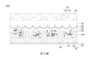
第3圖至第4圖繪示第2圖的全反射顯示器100運作時的示意圖。請參照第3圖,全反射顯示器100更包括第一透鏡層160、第二透明電極170以及第二介電層180。第一透鏡層160設置於子畫素190與顯示介質層150之間。舉例來說,第一透鏡層160的材質可為高折射率透鏡。第二透明電極170位於第一透鏡層160與顯示介質層150之間。第二介電層180位於第二透明電極170與顯示介質層150之間。第一介電層130延伸覆蓋反射層120的頂面122與側壁124,且第一介電層130與第一透鏡層160分開。在本實施方式中,當位於第一透鏡層160與第二介電層180之間的第二透明電極170提供正電位且薄膜電晶體基板110的第一透明電極112提供負電位時,顯示介質層150中的帶電黑色粒子移動至第二介電層180上以吸收光線L,可視為全反射顯示器100的暗態。FIG. 3 to FIG. 4 are schematic diagrams illustrating the operation of the
請參照第4圖,當位於第一透鏡層160與第二介電層180之間的第二透明電極170提供負電位且薄膜電晶體基板110的第一透明電極112提供正電位時,顯示介質層150中的帶電黑色粒子移動至子畫素190的黑色矩陣194下方的第一介電層130上(例如沿第一立體電極140設置的第一介電層130上),光線L在第一透鏡層160產生反射以及在反射層120產生反射,可視為全反射顯示器100的亮態。由於顯示介質層150中的帶電黑色粒子移動至黑色矩陣194下方的第一介電層130上,可降低帶電黑色粒子停留於濾光片192下方的第一介電層130上的比例,以提高亮態反射率。Please refer to Fig. 4, when the
應理解到,已敘述的元件連接關係與功效將不重覆贅述,合先敘明。在以下敘述中,將說明全反射顯示器的其他形式。It should be understood that the connection relationship and functions of the components that have been described will not be repeated, and will be described first. In the following description, other forms of fully reflective displays will be described.
第5圖繪示根據本揭露另一實施方式之全反射顯示器100a的剖面圖。請參照第5圖,其與第2圖之實施方式不同地方在於,第一介電層130接觸第一透鏡層160,並且第一介電層130以及第一立體電極140皆與薄膜電晶體基板110分開。全反射顯示器100更包括第三介電層130a,第三介電層130a覆蓋反射層120的頂面122與側壁124以及薄膜電晶體基板110的頂面114。第一立體電極140可使用接線方式電性連接薄膜電晶體基板110的第一透明電極112。在本實施方式中,當第二透明電極170提供正電位且電性連接第一透明電極112的第一立體電極140提供負電位時,顯示介質層150中的帶電黑色粒子移動至第二介電層180上,可視為全反射顯示器100的暗態。當第二透明電極170提供負電位且電性連接第一透明電極112的第一立體電極140提供正電位時,顯示介質層150中的帶電黑色粒子移動至第一介電層130上(例如沿第一立體電極140設置的第一介電層130上),可視為全反射顯示器100的亮態。FIG. 5 shows a cross-sectional view of a
第6圖繪示根據本揭露又一實施方式之全反射顯示器100b的剖面圖。請參照第6圖,其與第2圖之實施方式不同地方在於全反射顯示器100b不具有第2圖的第一透鏡層160、第二透明電極170以及第二介電層180,且全反射顯示器100b還包括第二透鏡層160b以及第三透明電極170b,第二透鏡層160b位於薄膜電晶體基板110與反射層120b之間。第二透鏡層160b與反射層120b之間可具有低折射率介質。舉例來說,第二透鏡層160b與反射層120b之間可具有空氣間隙,並且反射層120b的寬度W5大於第三透明電極170b的寬度W6。此外,第三透明電極170b位於顯示介質層150與薄膜電晶體基板110之間。第三透明電極170b與子畫素190分開,且第一介電層130延伸至第三透明電極170b上。FIG. 6 shows a cross-sectional view of a
在本實施方式中,當第三透明電極170b提供正電位且電性連接第一透明電極112的第一立體電極140提供負電位時,顯示介質層150中的帶電黑色粒子移動至第三透明電極170b上方的第一介電層130上(例如沿第一立體電極140設置的第一介電層130上),可視為全反射顯示器100的暗態。當第三透明電極170b提供負電位且電性連接第一透明電極112的第一立體電極140提供正電位時,顯示介質層150中的帶電黑色粒子移動至子畫素190的黑色矩陣194下方的第一介電層130上,可視為全反射顯示器100的亮態。In this embodiment, when the third
第7圖繪示根據本揭露再一實施方式之全反射顯示器100c的剖面圖。請參照第7圖,其與第6圖之實施方式不同地方在於,第一介電層130覆蓋薄膜電晶體基板110,且第三透明電極170b位於子畫素190與顯示介質層150之間並與第一介電層130分開。此外,全反射顯示器100c還包括第四介電層130c。第四介電層130c覆蓋第三透明電極170b,且顯示介質層150位於第四介電層130c與第一介電層130之間。FIG. 7 shows a cross-sectional view of a
在本實施方式中,當第三透明電極170b提供正電位且電性連接第一透明電極112的第一立體電極140提供負電位時,顯示介質層150中的帶電黑色粒子移動至第四介電層130c上,可視為全反射顯示器100的暗態。當第三透明電極170b提供負電位且電性連接第一透明電極112的第一立體電極140提供正電位時,顯示介質層150中的帶電黑色粒子移動至子畫素190的黑色矩陣194下方的第一介電層130上(例如沿第一立體電極140設置的第一介電層130上),可視為全反射顯示器100的亮態。In this embodiment, when the third
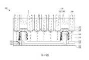
第8圖繪示第1圖沿線8-8之全反射顯示器100的剖面圖。詳細來說,第8圖進一步繪示全反射顯示器100的子畫素190的外圍區域。請參照第8圖,全反射顯示器100更包括檔牆300。檔牆300設置於第二介電層180與薄膜電晶體基板110之間,且檔牆300位於子畫素190的外圍處。檔牆300可提供分隔效果,使顯示介質層150中的帶電黑色粒子可在顯示介質層150的低折射率介質中移動。FIG. 8 shows a cross-sectional view of the
第9圖繪示根據本揭露另一實施方式之全反射顯示器100d的剖面圖。請參照第9圖,其與第8圖之實施方式不同地方在於,全反射顯示器100d還包括第二立體電極140d。第二立體電極140d設置於檔牆300中。第9圖僅繪示第二立體電極140d之半寬度W7。在本實施方式中,第一立體電極140的寬度W1(見第2圖)在1μm至32μm的範圍中,並且第二立體電極140d之半寬度W7的兩倍在1μm至32μm的範圍中。由於第一立體電極140的寬度W1與第二立體電極140d之半寬度W7的兩倍決定全反射顯示器100d的開口率,當第一立體電極140的寬度W1與第二立體電極140d之半寬度W7較窄時,可設置較寬的反射層120,以提高全反射顯示器100d的開口率,並增加全反射顯示器100d的亮態反射率。FIG. 9 shows a cross-sectional view of a
前述概述了幾個實施方式的特徵,使得本領域技術人員可以更好地理解本揭露的態樣。本領域技術人員應當理解,他們可以容易地將本揭露用作設計或修改其他過程和結構的基礎,以實現與本文介紹的實施方式相同的目的和/或實現相同的優點。本領域技術人員還應該認識到,這樣的等效構造不脫離本揭露的精神和範圍,並且在不脫離本揭露的精神和範圍的情況下,它們可以在這裡進行各種改變,替換和變更。The foregoing outlines features of several embodiments so that those skilled in the art may better understand aspects of the present disclosure. It should be appreciated by those skilled in the art that they may readily use the present disclosure as a basis for designing or modifying other processes and structures, so as to achieve the same purposes and/or achieve the same advantages as the embodiments described herein. Those skilled in the art should also realize that thisSuch equivalent constructions do not depart from the spirit and scope of the present disclosure, and they may be subject to various changes, substitutions and alterations herein without departing from the spirit and scope of the present disclosure.
100,100a,100b,100c,100d:全反射顯示器100, 100a, 100b, 100c, 100d: total reflection display
110:薄膜電晶體基板110: thin film transistor substrate
112:第一透明電極112: the first transparent electrode
114:頂面114: top surface
120,120b:反射層120,120b: reflective layer
122:頂面122: top surface
124:側壁124: side wall
130:第一介電層130: the first dielectric layer
130a:第三介電層130a: the third dielectric layer
130c:第四介電層130c: the fourth dielectric layer
140:第一立體電極140: the first three-dimensional electrode
140d:第二立體電極140d: the second three-dimensional electrode
150:顯示介質層150:Display medium layer
160:第一透鏡層160: the first lens layer
160b:第二透鏡層160b: the second lens layer
170:第二透明電極170: second transparent electrode
170b:第三透明電極170b: the third transparent electrode
180:第二介電層180: second dielectric layer
190:子畫素190: sub-pixel
192:濾光片192: Optical filter
194:黑色矩陣194: black matrix
200:前光模組200: Front light module
300:擋牆300: retaining wall
H1:高度H1: height
H2:厚度H2: Thickness
L:光線L: light
W1:寬度W1: width
W2:寬度W2: width
W3:寬度W3: width
W4:寬度W4: width
W5:寬度W5: width
W6:寬度W6: width
W7:半寬度W7: half width
2-2:線2-2: Line
8-8:線8-8: Line
當接合隨附諸圖閱讀時,得自以下詳細描述最佳地理解本揭露之一實施方式。應強調,根據工業上之標準實務,各種特徵並未按比例繪製且僅用於說明目的。事實上,為了論述清楚,可任意地增大或減小各種特徵之尺寸。 第1圖繪示根據本揭露一實施方式之全反射顯示器的子畫素的上視圖。 第2圖繪示第1圖沿線2-2之全反射顯示器的剖面圖。 第3圖至第4圖繪示第2圖的全反射顯示器運作時的示意圖。 第5圖繪示根據本揭露另一實施方式之全反射顯示器的剖面圖。 第6圖繪示根據本揭露又一實施方式之全反射顯示器的剖面圖。 第7圖繪示根據本揭露再一實施方式之全反射顯示器的剖面圖。 第8圖繪示第1圖沿線8-8之全反射顯示器的剖面圖。 第9圖繪示根據本揭露另一實施方式之全反射顯示器的剖面圖。One embodiment of the present disclosure is best understood from the following detailed description when read in conjunction with the accompanying drawings. It is emphasized that, in accordance with the standard practice in the industry, various features are not drawn to scale and are used for illustration purposes only. In fact, the dimensions of the various features may be arbitrarily increased or reduced for clarity of discussion. FIG. 1 shows a top view of a sub-pixel of a total reflection display according to an embodiment of the present disclosure. Fig. 2 shows a cross-sectional view of the total reflection display along line 2-2 in Fig. 1 . FIG. 3 to FIG. 4 are schematic diagrams illustrating the operation of the total reflection display in FIG. 2 . FIG. 5 shows a cross-sectional view of a total reflection display according to another embodiment of the present disclosure. FIG. 6 shows a cross-sectional view of a total reflection display according to yet another embodiment of the present disclosure. FIG. 7 shows a cross-sectional view of a total reflection display according to yet another embodiment of the present disclosure. Figure 8 shows a cross-sectional view of the total reflection display along line 8-8 of Figure 1 . FIG. 9 shows a cross-sectional view of a total reflection display according to another embodiment of the present disclosure.
國內寄存資訊(請依寄存機構、日期、號碼順序註記) 無 國外寄存資訊(請依寄存國家、機構、日期、號碼順序註記) 無Domestic deposit information (please note in order of depositor, date, and number) none Overseas storage information (please note in order of storage country, institution, date, and number) none
100:全反射顯示器100: Total reflection display
110:薄膜電晶體基板110: thin film transistor substrate
112:第一透明電極112: the first transparent electrode
114:頂面114: top surface
120:反射層120: reflective layer
122:頂面122: top surface
124:側壁124: side wall
130:第一介電層130: the first dielectric layer
140:第一立體電極140: the first three-dimensional electrode
150:顯示介質層150:Display medium layer
160:第一透鏡層160: the first lens layer
170:第二透明電極170: second transparent electrode
180:第二介電層180: second dielectric layer
190:子畫素190: sub-pixel
192:濾光片192: Optical filter
194:黑色矩陣194: black matrix
200:前光模組200: Front light module
H1:高度H1: height
H2:厚度H2: Thickness
W1:寬度W1: width
W2:寬度W2: width
W3:寬度W3: width
W4:寬度W4: width
Claims (14)
Translated fromChinesePriority Applications (3)
| Application Number | Priority Date | Filing Date | Title |
|---|---|---|---|
| TW110130000ATWI792493B (en) | 2021-08-13 | 2021-08-13 | Total internal reflection display |
| US17/513,150US11640097B2 (en) | 2021-08-13 | 2021-10-28 | Total internal reflection display |
| CN202111367992.8ACN114089576B (en) | 2021-08-13 | 2021-11-18 | Total reflection display |
Applications Claiming Priority (1)
| Application Number | Priority Date | Filing Date | Title |
|---|---|---|---|
| TW110130000ATWI792493B (en) | 2021-08-13 | 2021-08-13 | Total internal reflection display |
Publications (2)
| Publication Number | Publication Date |
|---|---|
| TWI792493Btrue TWI792493B (en) | 2023-02-11 |
| TW202307537A TW202307537A (en) | 2023-02-16 |
Family
ID=80301606
Family Applications (1)
| Application Number | Title | Priority Date | Filing Date |
|---|---|---|---|
| TW110130000ATWI792493B (en) | 2021-08-13 | 2021-08-13 | Total internal reflection display |
Country Status (3)
| Country | Link |
|---|---|
| US (1) | US11640097B2 (en) |
| CN (1) | CN114089576B (en) |
| TW (1) | TWI792493B (en) |
Families Citing this family (1)
| Publication number | Priority date | Publication date | Assignee | Title |
|---|---|---|---|---|
| TWI807728B (en)* | 2022-03-28 | 2023-07-01 | 友達光電股份有限公司 | Electrophoretic display device and driving method thereof |
Citations (5)
| Publication number | Priority date | Publication date | Assignee | Title |
|---|---|---|---|---|
| TW201024886A (en)* | 2008-12-29 | 2010-07-01 | Ind Tech Res Inst | Display structure |
| TWI468831B (en)* | 2010-02-12 | 2015-01-11 | Univ Nat Chiao Tung | Color pixel for a display |
| TWI493410B (en)* | 2013-10-08 | 2015-07-21 | E Ink Holdings Inc | Touch display device |
| TWI714063B (en)* | 2008-09-19 | 2020-12-21 | 日商半導體能源研究所股份有限公司 | Display device |
| CN113156732A (en)* | 2021-05-31 | 2021-07-23 | 京东方科技集团股份有限公司 | Reflective display panel, preparation method thereof and display device |
Family Cites Families (15)
| Publication number | Priority date | Publication date | Assignee | Title |
|---|---|---|---|---|
| KR100805161B1 (en) | 1999-03-15 | 2008-02-21 | 도판 인사츠 가부시키가이샤 | Electrode Board for Reflective Liquid Crystal Display and Reflective Liquid Crystal Display |
| CN100520552C (en) | 2005-04-15 | 2009-07-29 | 不列颠哥伦比亚大学 | Brightness enhancement in tir-modulated electrophoretic reflective image displays |
| KR20080111939A (en)* | 2007-06-20 | 2008-12-24 | 엘지디스플레이 주식회사 | Liquid crystal display |
| KR101677669B1 (en)* | 2009-11-02 | 2016-11-29 | 주식회사 동진쎄미켐 | Display device driven by electric field |
| US9366920B2 (en) | 2013-01-02 | 2016-06-14 | Lg Display Co., Ltd. | Liquid crystal display device and fabricating method thereof |
| CN103107285B (en)* | 2013-01-15 | 2015-08-26 | 大连龙宁科技有限公司 | A kind of stereo display electrode and manufacture method thereof |
| CN107111016B (en) | 2014-10-08 | 2020-08-28 | 协和(香港)国际教育有限公司 | Color filter aligned reflective display |
| CN105589252A (en)* | 2016-03-11 | 2016-05-18 | 京东方科技集团股份有限公司 | Light valve element and control method thereof and display device |
| US20190107765A1 (en) | 2016-05-23 | 2019-04-11 | Clearink Displays Inc. | Hybrid reflective-emissive image display |
| CN106154678A (en) | 2016-09-29 | 2016-11-23 | 京东方科技集团股份有限公司 | A kind of display device |
| CN106569365B (en)* | 2016-10-28 | 2019-02-22 | 京东方科技集团股份有限公司 | Reflective display and method of making the same |
| CN106842728A (en)* | 2017-04-06 | 2017-06-13 | 深圳市华星光电技术有限公司 | The preparation method of array base palte and the array base palte |
| CN208477259U (en) | 2018-04-25 | 2019-02-05 | 京东方科技集团股份有限公司 | A kind of reflective display screen and display device |
| CN108919586B (en)* | 2018-06-28 | 2021-09-28 | 上海天马微电子有限公司 | Display panel and display device |
| TWI720569B (en)* | 2019-08-02 | 2021-03-01 | 友達光電股份有限公司 | Display panel |
- 2021
- 2021-08-13TWTW110130000Apatent/TWI792493B/enactive
- 2021-10-28USUS17/513,150patent/US11640097B2/enactiveActive
- 2021-11-18CNCN202111367992.8Apatent/CN114089576B/enactiveActive
Patent Citations (5)
| Publication number | Priority date | Publication date | Assignee | Title |
|---|---|---|---|---|
| TWI714063B (en)* | 2008-09-19 | 2020-12-21 | 日商半導體能源研究所股份有限公司 | Display device |
| TW201024886A (en)* | 2008-12-29 | 2010-07-01 | Ind Tech Res Inst | Display structure |
| TWI468831B (en)* | 2010-02-12 | 2015-01-11 | Univ Nat Chiao Tung | Color pixel for a display |
| TWI493410B (en)* | 2013-10-08 | 2015-07-21 | E Ink Holdings Inc | Touch display device |
| CN113156732A (en)* | 2021-05-31 | 2021-07-23 | 京东方科技集团股份有限公司 | Reflective display panel, preparation method thereof and display device |
Also Published As
| Publication number | Publication date |
|---|---|
| US11640097B2 (en) | 2023-05-02 |
| CN114089576A (en) | 2022-02-25 |
| US20230052419A1 (en) | 2023-02-16 |
| TW202307537A (en) | 2023-02-16 |
| CN114089576B (en) | 2023-07-04 |
Similar Documents
| Publication | Publication Date | Title |
|---|---|---|
| CN110323354B (en) | Display panel and display device | |
| CN110266861B (en) | Display panel and display device | |
| CN113156732B (en) | Reflective display panel and manufacturing method thereof, and display device | |
| JPH1096910A (en) | Liquid crystal display device having micro lenses | |
| KR102797376B1 (en) | Display device and manufacturing method thereof | |
| TWI792493B (en) | Total internal reflection display | |
| CN115275067A (en) | Display panels and display devices | |
| WO2023246492A1 (en) | Display panel, display device, and vehicle-mounted display system | |
| CN116390564A (en) | Display panel and display device | |
| US20230247891A1 (en) | Display apparatus and electronic device | |
| WO2025167499A1 (en) | Display panel | |
| CN113569662B (en) | Fingerprint sensing device | |
| CN113759631B (en) | Display panel and manufacturing method thereof, and display device | |
| CN112130236B (en) | Low-reflection structure, display panel, display device, and manufacturing method of display panel | |
| TWI785478B (en) | Fingerprint sensing device | |
| CN114967271A (en) | A display module and display device | |
| CN117954561A (en) | Display Panel | |
| TW202023089A (en) | Flexible display | |
| KR20240103301A (en) | Optical member and display apparatus comprising the same | |
| US20250127020A1 (en) | Display module and preparation method therefor, and display device | |
| JP2007047495A (en) | Reflective display device and method of manufacturing reflective display device | |
| CN115273671A (en) | Display panel and display device | |
| US20200133057A1 (en) | Liquid crystal apparatus and electronic apparatus | |
| CN223207478U (en) | Display panel and display terminal | |
| US20240224751A1 (en) | Light emitting display device |