TWI790413B - Shield for a capacitive touch system - Google Patents
Shield for a capacitive touch systemDownload PDFInfo
- Publication number
- TWI790413B TWI790413BTW108147694ATW108147694ATWI790413BTW I790413 BTWI790413 BTW I790413BTW 108147694 ATW108147694 ATW 108147694ATW 108147694 ATW108147694 ATW 108147694ATW I790413 BTWI790413 BTW I790413B
- Authority
- TW
- Taiwan
- Prior art keywords
- touch sensor
- antenna
- radio frequency
- mask
- shield
- Prior art date
Links
Images


Classifications
- G—PHYSICS
- G06—COMPUTING OR CALCULATING; COUNTING
- G06F—ELECTRIC DIGITAL DATA PROCESSING
- G06F3/00—Input arrangements for transferring data to be processed into a form capable of being handled by the computer; Output arrangements for transferring data from processing unit to output unit, e.g. interface arrangements
- G06F3/01—Input arrangements or combined input and output arrangements for interaction between user and computer
- G06F3/03—Arrangements for converting the position or the displacement of a member into a coded form
- G06F3/041—Digitisers, e.g. for touch screens or touch pads, characterised by the transducing means
- G06F3/044—Digitisers, e.g. for touch screens or touch pads, characterised by the transducing means by capacitive means
- G—PHYSICS
- G06—COMPUTING OR CALCULATING; COUNTING
- G06F—ELECTRIC DIGITAL DATA PROCESSING
- G06F3/00—Input arrangements for transferring data to be processed into a form capable of being handled by the computer; Output arrangements for transferring data from processing unit to output unit, e.g. interface arrangements
- G06F3/01—Input arrangements or combined input and output arrangements for interaction between user and computer
- G06F3/03—Arrangements for converting the position or the displacement of a member into a coded form
- G06F3/033—Pointing devices displaced or positioned by the user, e.g. mice, trackballs, pens or joysticks; Accessories therefor
- G06F3/0354—Pointing devices displaced or positioned by the user, e.g. mice, trackballs, pens or joysticks; Accessories therefor with detection of 2D relative movements between the device, or an operating part thereof, and a plane or surface, e.g. 2D mice, trackballs, pens or pucks
- G06F3/03547—Touch pads, in which fingers can move on a surface
Landscapes
- Engineering & Computer Science (AREA)
- General Engineering & Computer Science (AREA)
- Theoretical Computer Science (AREA)
- Human Computer Interaction (AREA)
- Physics & Mathematics (AREA)
- General Physics & Mathematics (AREA)
- Position Input By Displaying (AREA)
- Switches That Are Operated By Magnetic Or Electric Fields (AREA)
- Details Of Aerials (AREA)
Abstract
Translated fromChineseDescription
Translated fromChinese本發明總體涉及電容式感測器,諸如觸控板以及操作方法。更具體地,本發明涉及通過觸控板能夠發射和接收射頻的系統及其方法。The present invention generally relates to capacitive sensors, such as touchpads, and methods of operation. More particularly, the present invention relates to a system capable of transmitting and receiving radio frequency through a touch panel and a method thereof.
觸控板通常包括在基於處理器的裝置,諸如筆記型電腦等上,以允許用戶將手指、手寫筆等用作輸入和選擇的來源。此外,基於處理器的裝置通常包括用於WiFi、藍牙、近場通信(NFC)等的射頻(例如,3MHz-30GHz)發射器、接收器、收發器等(統稱為「收發器」)。然而,電容式觸控板通常需要電遮罩體,以防止來自基於處理器的裝置的雜訊干擾正常的觸控板功能。當靠近無線電收發器時,該遮罩體可能會阻止射頻的發射和接收。Touchpads are often included on processor-based devices, such as laptop computers, to allow users to use fingers, stylus, etc. as a source of input and selection. In addition, processor-based devices typically include radio frequency (eg, 3MHz-30GHz) transmitters, receivers, transceivers, etc. (collectively "transceivers") for WiFi, Bluetooth, near field communication (NFC), and the like. However, capacitive touchpads typically require an electrical shield to prevent noise from the processor-based device from interfering with normal touchpad functionality. When in close proximity to a radio transceiver, the shield may block radio frequency transmission and reception.
例如,觸控板可能是基於處理器的裝置(諸如膝上型電腦)的底座中的唯一開口,並且該單個開口可以用於多種目的,例如發送和接收WiFi或NFC通信。現有裝置可以將射頻天線放置在觸控板附近(例如,下方),並且將觸控板接地平面遮罩體填充圖案(hatch),以使某些射頻穿過遮罩體。但是,這種方法通常需要調諧天線以發射穿過遮罩體,而調諧通常很困難。此外,天線系統可能會比典型安裝浪費更多的電能,並且觸控板的性能可能仍會受到影響。另外,由於觸控板印刷電路板(PCB)中的變化影響天線諧振,上述系統可能更難以製造。現有裝置及方法還存在其它缺陷、不便以及問題。For example, a trackpad may be the only opening in the base of a processor-based device such as a laptop, and this single opening may be used for multiple purposes, such as sending and receiving WiFi or NFC communications. Existing devices can place the RF antenna near (eg, below) the touchpad, and hatch the touchpad ground plane so that some of the RF passes through the hatch. However, this approach typically requires tuning the antenna to transmit through the shroud, which is often difficult. Also, the antenna system may waste more power than a typical installation, and the performance of the trackpad may still suffer. Additionally, the system described above can be more difficult to manufacture due to variations in the touchpad printed circuit board (PCB) that affect antenna resonance. Other deficiencies, inconveniences, and problems exist with existing devices and methods.
因此,揭露的實施例解決了現有裝置及方法的上述以及其它缺點、不便和問題。所揭露的實施例包括觸摸感測器系統和方法,該觸摸感測器系統包括可以放置在觸控板上或非常靠近觸控板的射頻天線。觸控板感測器包括圖案化遮罩體,該圖案化遮罩體遮罩觸控板感測器免受後側信號的影響,並且具有大到足以允許射頻通過觸控板感測器的開口。圖案化遮罩體利用層替換典型的接地平面,該層被設計成遮罩互電容結,但使每個觸控板感測器單元的中央保持敞開狀態(以允許射頻通過)。另外,圖案化遮罩體被劃分為遮罩各個感測器結的各個單元。可以以使NFC天線的感應電流最小並且減少NFC系統的電能的圖案連接遮罩體單元。在一些情況下,徑向連接遮罩體單元可以使感應電流最小。在其它例子中,可以以其它配置連接遮罩體單元以減小感應電流。還存在其它實施例、優點和特徵。Accordingly, the disclosed embodiments address the above and other disadvantages, inconveniences and problems of prior devices and methods. Disclosed embodiments include touch sensor systems and methods that include radio frequency antennas that can be placed on or in close proximity to a touchpad. The touchpad sensor includes a patterned shroud that shields the touchpad sensor from rear side signals and has an Open your mouth. The patterned mask replaces the typical ground plane with a layer designed to mask the mutual capacitance junction but leave the center of each touchpad sensor cell open (to allow RF to pass through). In addition, the patterned mask volume is divided into individual cells that mask individual sensor junctions. The mask unit may be connected in a pattern that minimizes the induced current of the NFC antenna and reduces the power of the NFC system. In some cases, connecting the shield elements radially can minimize induced currents. In other examples, the shield units may be connected in other configurations to reduce induced currents. Other embodiments, advantages and features also exist.
在一些例子中,一種設備可以包括觸摸感測器;第一天線;遮罩體結構,定位在觸摸感測器和第一天線之間;以及至少一個射頻透過(radio frequency transparent)部,整合到遮罩體結構中。In some examples, an apparatus may include a touch sensor; a first antenna; a shield structure positioned between the touch sensor and the first antenna; and at least one radio frequency transparent portion, Integrate into mask structure.
遮罩體結構可以包括沉積在電絕緣材料上的金屬層,並且射頻透過部包括在金屬層中限定的開口。The mask structure may include a metal layer deposited on an electrically insulating material, and the radio frequency transmissive portion includes openings defined in the metal layer.
觸摸感測器可以包括在第一電極和第二電極之間的互電容交叉點;射頻透過部偏離互電容交叉點。The touch sensor may include a mutual capacitance intersection between the first electrode and the second electrode; the radio frequency transparent portion is offset from the mutual capacitance intersection.
金屬層可以與互電容交叉點重疊。Metal layers may overlap mutual capacitance intersections.
金屬層可以具有與互電容交叉點重疊的增大區域。The metal layer may have an enlarged area overlapping the mutual capacitance intersection.
觸摸感測器可以包括與第一天線間隔開第一距離的第一互電容交叉點和與第一天線間隔開第二距離的第二互電容交叉點,其中第二距離比第一距離距第一天線更遠。The touch sensor may include a first mutual capacitance spaced a first distance from the first antennaThe intersection and the second mutual capacitance intersection are spaced apart from the first antenna by a second distance, wherein the second distance is further from the first antenna than the first distance.
觸摸感測器可以包括與第一互電容交叉點重疊的遮罩體結構的第一金屬層區域,第一金屬層區域小於與第二互電容交叉點重疊的遮罩體結構的第二金屬層區域。The touch sensor may include a first metal layer area of the mask structure overlapping the first mutual capacitance intersection, the first metal layer area being smaller than a second metal layer of the mask structure overlapping the second mutual capacitance intersection area.
遮罩體結構可以進一步包括沉積在電絕緣材料上的金屬層,並且射頻透過部包括在金屬層中限定的多個遮罩體開口。The shroud structure may further include a metal layer deposited on the electrically insulating material, and the radio frequency transmissive portion includes a plurality of shroud openings defined in the metal layer.
多個遮罩體開口中的至少一些可以隨著與第一天線的距離的增加而逐漸變小。At least some of the plurality of shroud openings may taper with increasing distance from the first antenna.
遮罩體結構可以包括第一區域和第二區域,該第一區域具有第一尺寸的第一子組遮罩體開口,該第二區域具有第二尺寸的第二子組遮罩體開口,其中第一區域比第二區域距第一天線更近,並且其中第一尺寸大於第二尺寸。在一些情況下,在整個第一區域統一使用第一尺寸,在整個第二區域統一使用第二尺寸。在其它例子中,尺寸可以在距離上從第一尺寸過渡到第二尺寸。The mask structure may include a first region having a first subset of mask openings of a first size and a second region having a second subset of mask openings of a second size, Wherein the first area is closer to the first antenna than the second area, and wherein the first size is greater than the second size. In some cases, the first size is uniformly used throughout the first area, and the second size is uniformly used throughout the second area. In other examples, the dimensions may transition in distance from a first dimension to a second dimension.
該裝置可以包括第二天線和整合到遮罩體結構中的第二射頻透過部,可以至少部分地根據與第二天線的接近度設計該第二射頻透過部的尺寸。可以至少部分地根據與第一天線的接近度來設計第一射頻透過部的尺寸。The apparatus may include a second antenna and a second radio frequency transparent portion integrated into the shield structure, the second radio frequency transparent portion may be dimensioned at least in part based on proximity to the second antenna. The first radio frequency transparent portion may be dimensioned at least in part based on proximity to the first antenna.
在一些例子中,一種設備可以包括觸摸感測器;天線;遮罩體結構,定位在觸摸感測器和第一天線之間;以及圖案化遮罩區域,整合到遮罩體結構中。In some examples, an apparatus can include a touch sensor; an antenna; a shroud structure positioned between the touch sensor and the first antenna; and a patterned shroud region integrated into the shroud structure.
圖案化遮罩區域可以由在導電材料中限定的開口分隔開。The patterned mask regions may be separated by openings defined in the conductive material.
圖案化遮罩區域可以被定位成遮罩觸摸感測器的互電容結,同時使至少一些觸摸感測器單元的中央敞開以允許射頻通過。The patterned mask area can be positioned to mask the mutual capacitance junction of the touch sensor whileThe center of at least some of the touch sensor units is left open to allow radio frequency passage.
圖案化遮罩區域可以被定位成遮罩各個感測器結。Patterned masking regions can be positioned to mask individual sensor junctions.
天線可以被配置成發射WiFi信號。Antennas may be configured to transmit WiFi signals.
可以徑向連接圖案化遮罩區域。The patterned mask regions may be connected radially.
圖案化遮罩區域可以被配置成使來自近場通信天線的感應電流最小並且減少近場通信系統的電能。The patterned mask area can be configured to minimize induced currents from near field communication antennas and reduce near field communication system power.
在一些例子中,設備可以包括觸摸感測器、天線、定位在觸摸感測器和天線之間的遮罩體結構、以及在遮罩體結構的導電層中限定的多個遮罩體開口,遮罩體開口大到足以允許射頻通過遮罩體結構。In some examples, the device may include a touch sensor, an antenna, a cover structure positioned between the touch sensor and the antenna, and a plurality of cover openings defined in a conductive layer of the cover structure, The shield opening is large enough to allow radio frequencies to pass through the shield structure.
導電層可以利用與觸摸感測器中的電極的柵重疊定位的多個垂直列和多個水平行限定遮罩體開口。The conductive layer may define a mask opening with a plurality of vertical columns and a plurality of horizontal rows positioned overlapping a grid of electrodes in the touch sensor.
多個遮罩體開口可以位於觸摸感測器的靠近天線的第一區域中,並且遮罩體結構包括觸摸感測器的第二區域中的沒有遮罩體開口的固態導電層,該第二區域比第一區域與天線間隔更遠。A plurality of shroud openings may be located in a first area of the touch sensor near the antenna, and the shroud structure includes a solid conductive layer without shroud openings in a second area of the touch sensor, the second The regions are spaced farther from the antenna than the first region.
100:互電容感測裝置100: Mutual capacitance sensing device
10、26:觸控板10, 26: Touchpad
12、121:行電極12, 121: row electrodes
14:列電極14: column electrode
16:觸摸控制器16: Touch controller
18:接地平面遮罩體18: Ground plane mask body
20:膝上型電腦20: Laptop
22:顯示器22: Display
24:鍵盤24: keyboard
28:射頻發射器28:RF Transmitter
30、40、50:觸控板遮罩體30, 40, 50: touchpad cover body
32:垂直行32: vertical row
34、120:水平行34, 120: horizontal row
36、46、56:結36, 46, 56: Knots
38、48、58:中央38, 48, 58: Central
102:觸摸感測器102: Touch sensor
104:發射電極104: Emitter electrode
106:感測電極106: sensing electrode
108:互電容交叉點108: Mutual capacitance intersection point
110:導電層110: conductive layer
112:限定開口112: limited opening
114:窄截面寬度114: narrow section width
116:圖案化遮罩區域116: Patterned mask area
118:沿垂直列118: along the vertical column
200:堆疊部200: stacking department
202:遮罩體結構202: Mask structure
204:基板204: Substrate
206:第一側206: First side
208:第一組電極208: The first set of electrodes
210:第二側210: second side
212:第二組電極212: The second set of electrodes
214:電絕緣材料214: electrical insulating material
216:導電材料216: Conductive material
218:遠側218: far side
300:第一天線300: the first antenna
302:第二天線302: second antenna
303、305:邊界區域303, 305: Boundary area
304:第一區域304: the first area
306:第二區域306: second area
308:第三區域308: The third area
400:天線400: Antenna
1700-1702:方法1700-1702: Methods
圖1描繪電容式觸控板系統的例子。Figure 1 depicts an example of a capacitive touchpad system.
圖2描繪根據所揭露實施例的包括觸控板和射頻發射器的基於處理器的設備的例子。2 depicts an example of a processor-based device including a touchpad and a radio frequency transmitter in accordance with disclosed embodiments.
圖3描繪根據所揭露實施例的觸控板遮罩體的例子。FIG. 3 depicts an example of a touchpad cover according to disclosed embodiments.
圖4描繪根據所揭露實施例的觸控板遮罩體的例子。FIG. 4 depicts an example of a touchpad cover according to disclosed embodiments.
圖5描繪根據所揭露實施例的觸控板遮罩體的例子。FIG. 5 depicts an example of a touchpad cover according to disclosed embodiments.
圖6描繪根據所揭露實施例的遮罩體結構的例子。FIG. 6 depicts an example of a mask structure according to disclosed embodiments.
圖7描繪根據所揭露實施例的遮罩體結構的例子。FIG. 7 depicts an example of a mask structure according to disclosed embodiments.
圖8描繪根據所揭露實施例的遮罩體結構的例子。FIG. 8 depicts an example of a mask structure according to disclosed embodiments.
圖9描繪根據所揭露實施例的遮罩體結構的例子。FIG. 9 depicts an example of a mask structure according to disclosed embodiments.
圖10描繪根據所揭露實施例的遮罩體結構的例子。FIG. 10 depicts an example of a mask structure according to disclosed embodiments.
圖11描繪根據所揭露實施例的遮罩體結構的例子。FIG. 11 depicts an example of a mask structure according to disclosed embodiments.
圖12描繪根據所揭露實施例的遮罩體結構的例子。Figure 12 depicts an example of a mask structure according to disclosed embodiments.
圖13描繪根據所揭露實施例的遮罩體結構的例子。Figure 13 depicts an example of a mask structure according to disclosed embodiments.
圖14描繪根據所揭露實施例的遮罩體結構的例子。FIG. 14 depicts an example of a mask structure according to disclosed embodiments.
圖15描繪根據所揭露實施例的遮罩體結構的例子。Figure 15 depicts an example of a mask structure according to disclosed embodiments.
圖16描繪根據所揭露實施例的遮罩體結構的例子。Figure 16 depicts an example of a mask structure according to disclosed embodiments.
圖17描繪根據所揭露實施例的用於發射無線信號的方法的例子。Figure 17 depicts an example of a method for transmitting wireless signals according to disclosed embodiments.
雖然本發明內容易於有各種修改形式和替代形式,但是在圖式中通過例子的方式示出具體實施例,並且在本文將對其進行詳細描述。然而,應當理解的是,本發明的內容並不旨在限於所揭露的特定形式。相反,其意圖是涵蓋落入由所附請求項書限定的本發明的精神和範圍內的所有修改方案、等同方案和替代方案。While the disclosure is susceptible to various modifications and alternative forms, specific embodiments have been shown by way of example in the drawings and herein will be described in detail. It should be understood, however, that the invention is not intended to be limited to the particular forms disclosed. On the contrary, the intention is to cover all modifications, equivalents, and alternatives falling within the spirit and scope of the invention as defined by the appended claims.
該描述提供了各種例子,並不旨在限制本發明的範圍、適用性或配置。相反,後續描述將向本領域具有通常知識者提供能夠實施本發明的實施例的描述。可以對元件的功能和佈置進行各種改變。This description provides various examples, and is not intended to limit the scope, applicability or configuration of the invention. Rather, the ensuing description will provide those of ordinary skill in the art with implementations that enable the invention to be practiced.Example description. Various changes may be made in the function and arrangement of elements.
因此,各種實施例可以適當地省略、替代或添加各種過程或元件。例如,應理解的是,可以以與所描述的順序不同的循序執行所述方法,並且可以添加、省略或組合各種步驟。而且,關於一些實施例所描述的方面和元件可以在各種其它實施例中進行組合。還應理解的是,以下系統、方法、裝置和軟體可以單獨或共同地作為較大系統的元件,其中其它過程可以優先於或以其它方式修改其應用。Therefore, various embodiments may omit, substitute, or add various procedures or elements as appropriate. For example, it should be understood that the methods may be performed in an order different from that described, and that various steps may be added, omitted, or combined. Furthermore, aspects and elements described with respect to some embodiments may be combined in various other embodiments. It should also be understood that the following systems, methods, apparatus, and software may individually or collectively be elements of a larger system where other processes may override or otherwise modify their application.
為了本發明的目的,術語「對準」通常是指平行、基本平行、或形成小於35.0度的角度。為了本發明的目的,術語「橫向」通常是指垂直、基本垂直、或形成55.0度至125.0度之間的角度。為了本發明的目的,術語「長度」通常是指物體的最長尺寸。為了本發明的目的,術語「寬度」通常是指物體從一側到另一側的尺寸,並且可以指穿過垂直於該物體的長度的物體測量。For purposes of the present invention, the term "aligned" generally means parallel, substantially parallel, or forming an angle of less than 35.0 degrees. For purposes of the present invention, the term "transverse" generally means perpendicular, substantially perpendicular, or forming an angle between 55.0 degrees and 125.0 degrees. For the purposes of the present invention, the term "length" generally refers to the longest dimension of an object. For the purposes of the present invention, the term "width" generally refers to the dimension of an object from side to side, and may refer to a measurement across an object perpendicular to the length of the object.
為了本發明的目的,術語「電極」通常是指意在用於進行測量的電導體的一部分,並且術語「路線」和「跡線」通常是指電導體的無意進行測量的部分。為了本發明相關電路的目的,術語「線」通常是指電極和電導體的「路線」或「路徑」部分的組合。為了本發明的目的,術語「Tx」通常是指發射線,並且術語「Rx」通常是指感測線。For the purposes of the present invention, the term "electrode" generally refers to a portion of an electrical conductor intended for measurement, and the terms "route" and "trace" generally refer to a portion of an electrical conductor where measurement is not intended. For the purposes of the present invention in relation to circuits, the term "wire" generally refers to a combination of electrodes and "route" or "path" portions of electrical conductors. For purposes of this disclosure, the term "Tx" generally refers to a transmit line, and the term "Rx" generally refers to a sense line.
應理解的是,在整個文檔中術語「觸摸感測器」的使用可以與「電容式觸摸感測器」、「電容式感測器」、「電容式觸摸和接近感測器」、「接近感測器」、「觸摸和接近感測器」、「觸摸面板」、「觸控板」和「觸控式螢幕」互換使用。It should be understood that throughout this document the term "touch sensor" is used interchangeably with "capacitive touch sensor", "capacitive sensor", "capacitive touch and proximity sensor", "proximity Sensor, touch and proximity sensor, touch panel, trackpad, and touchscreen are used interchangeably.
還應理解的是,如在本文中所使用的,術語「垂直」、「水準」、「橫向」、「上」、「下」、「左」、「右」、「內」、「外」等可以指所揭露裝置和/或圖式中所示的元件中的特徵的相對方向或位置。例如,「上」或「最上」可以指比另一特徵更靠近頁面頂部的特徵。然而,這些術語應當廣義地解釋為包括具有諸如一下的其它方位的設備和/或元件:頂/底、上面/下面、上方/下方、上/下和左/右可以根據該方位而互換的顛倒或傾斜的方位。It should also be understood that, as used herein, the terms "vertical", "horizontal","Lateral," "upper," "lower," "left," "right," "inner," "outer," etc. may refer to the relative orientation or orientation of features in disclosed devices and/or elements shown in the drawings. Location. For example, "top" or "topmost" may refer to a feature that is closer to the top of the page than another feature. However, these terms should be broadly interpreted to include devices and/or elements having other orientations such as: top/bottom, above/below, above/below, up/down, and left/right reversed where the orientation may be interchanged or tilted orientation.
本發明利用了CIRQUE®公司的觸控板技術。因此,在一定程度上理解觸控板技術的操作是有用的。CIRQUE®公司的觸控板技術是互電容感測裝置100,並且在圖1中示出例子。對於該互電容感測裝置100,使用具有行電極12和列電極14的柵的觸控板10來限定觸控板10的觸摸敏感區域。通常,觸控板被配置成適當數量(例如8×6、16×12、9×15等)的電極的矩形柵。The present invention utilizes touchpad technology from CIRQUE® Corporation. Therefore, it is useful to have some understanding of the operation of trackpad technology. A touchpad technology from CIRQUE® Corporation is a mutual
如圖1所示,互電容感測裝置100還包括觸摸控制器16。觸摸控制器16通常包括中央處理器(CPU)、數位訊號處理器(DSP),包括放大器的模擬前端(AFE)、週邊介面控制器(PIC)、另一種類型的微處理器和/或它們的組合中的至少一個,並且可以利用根據可用操作模式選擇的適當電路、硬體、固件和/或軟體被實施為積體電路、現場可程式設計閘陣列(FPGA)、專用積體電路(ASIC)、邏輯門電路的組合、其它類型的數位或類比電氣設計元件或它們的組合。As shown in FIG. 1 , the mutual
通常,觸摸控制器16還包括使行電極12或列電極14交替用作驅動電極或感測電極的至少一個多工電路。可以按順序或隨機一次驅動一個驅動電極,或者以編碼的模式同時驅動所有驅動電極。諸如同時驅動和感測電極的自電容模式的其它配置也是可能的。電極也可以以非矩形陣列,例如徑向圖案、線性串等佈置。還如圖1所示,接地平面遮罩體18可以設置在電極12、14下方,以減少雜訊或其它干擾。接地平面遮罩體18被示出為延伸在電極12、14之外僅是為了便於說明。其它配置也是可能的。Typically,
通常,不使用固定參考點進行測量。觸摸控制器16生成以各種模式直接發送到行電極12和列電極14的信號。Typically, measurements are made without a fixed reference point.
觸控板10不依賴於絕對電容測量來確定觸控板10表面上的手指(或手寫筆、指標或其它目標)的位置。觸控板10測量到用作感測電極的電極(例子性地示出為圖1的行電極121,但是可以是行電極12、列電極14或其它專用感測電極中的任意一個)的電荷不平衡。當在觸控板10上或附近沒有指示目標時,觸摸控制器16處於平衡狀態,並且在感測電極(例如,電極121)上沒有信號。當由於電容耦合導致手指或其它指示目標產生失衡不平衡時,則構成觸控板電極柵的多個電極12、14上發生電容的變化。所測量的是電容的變化,而不是電極12、14的絕對電容值。The
圖2是根據所揭露實施例的包括觸控板26和射頻發射器28的基於處理器的裝置的示意性俯視圖。如該實施例所示,基於處理器的裝置可以是具有顯示器22、鍵盤24和觸控板26的膝上型電腦20。FIG. 2 is a schematic top view of a processor-based device including a
再如圖所示,膝上型電腦20還可以包括射頻收發器28。在圖2的實施例中,射頻收發器28以虛線示出以指示它在觸控板26下方,然而,該位置僅僅是例子性的,並且可以使用其它位置。另外,可以使用多個射頻收發器28,或者可以使用單獨的發射器和接收器。Also as shown, the
同樣地,正如受益於本發明的本領域普通具有通常知識者將理解的是,射頻收發器28的類型隨裝置的功能而變化。例如,對於NFC應用,射頻收發器28可以在13.5MHz的頻率範圍內操作;對於藍牙應用,射頻收發器28可以在2.4GHz至2.5GHz的範圍內操作;並且對於WiFi應用,收發器28可以在2.4GHz、5GHz或其它頻率的範圍內操作。其它應用和頻率範圍也是可能的。Likewise, the type of
圖3是根據所揭露實施例的觸控板遮罩體30的示意性俯視圖。如本文所揭露的,實心的或填充圖案的接地平面遮罩體(例如,接地平面遮罩體18)可能干擾射頻收發器28等通常採用的較高射頻,然而,接地平面遮罩體需要遮罩觸控板免受雜訊和其它干擾的影響,以使觸控板可以正常工作。因此,觸控板遮罩體30被設計為在較高頻率(例如對於NFC,為13.5MHz;對於WiFi,為900MHz、2.4GHz、5GHz等)下具有高阻抗,並且在觸控板的工作頻率(例如100kHz至3MHz)下具有低阻抗。FIG. 3 is a schematic top view of a
在一些情況下,觸控板遮罩體30可以被構造成用作為觸摸感測器電極層(例如,電極12和14)的投影或組合的另一層代替典型的實心的或填充圖案的接地平面遮罩體18。在其它例子中,觸控板遮罩體可以具有被構造成遮罩結區域而不遮罩遠離結點的區域的形狀。在圖3所示的例子中,遮罩體材料的多個垂直行32和水平行34可被製成放置在相應電極12、14層之下。遮罩體材料可以包括銅、鋁或其它適當的遮罩體材料,並且可以蝕刻、印刷或以其他方式沉積在基板上。如圖所示,觸控板遮罩體30具體遮罩了電極(例如電極12、14)重疊的互電容結(例如結36),但使得每個感測器單元的中央(例如中央38)敞開以允許射頻通過。另外,圖案化遮罩體被劃分為遮罩各個感測器結點的各個單元。在一些實施例中,可以連接遮罩體單元以減小來自NFC天線等的感應電流和/或使來自NFC天線等的感應電流最小,並且減少NFC系統的電能。在一些情況下,可以徑向地、垂直地連接,或以其它佈置方式連接單元以減小感應電流。圖3中針對觸控板遮罩體30示出的特定形狀和矩形柵僅是例子性的,並且可以使用其它形狀和圖案。In some cases,
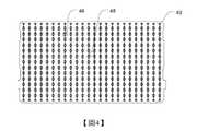
例如,圖4和圖5示出根據所揭露實施例的可以使用的其它例子性形狀和圖案。圖4示出具有相對較小的結46和相對較大的敞開中央48的觸控板遮罩體40的實施例,並且圖5示出具有相對較密的結56和相對較小的敞開中央58的觸控板遮罩體50的實施例。正如受益於本發明的本領域具有通常知識者將理解的是,取決於特定的基於處理器的裝置、觸控板、收發器等中所涉及的功能和頻率,可以採用其它形狀、圖案、結、敞開中央等。For example, FIGS. 4 and 5 illustrate other exemplary shapes and patterns that may be used in accordance with disclosed embodiments. FIG. 4 shows an embodiment of a
圖6描繪觸摸感測器102的電極的柵的例子。在該例子中,多個發射電極104設置在基板上,並且正交佈置的感應電極106也設置在基板上。發射電極104和感測電極106彼此重疊,但是彼此電隔離,藉以形成互電容交叉點108。在一些情況下,藉由基板提供電絕緣,其中發射電極104設置在基板的第一側上,感測電極106設置在基板的第二側上。在一些情況下,當第一發射電極上的電壓改變時,與第一發射電極交叉的每個感測電極上的電容在電極相交的交叉點處改變。此外,當導電目標接近觸摸感測器時,觸摸或接近觸摸感測器的目標附近的互電容交叉點具有電容的變化。FIG. 6 depicts an example of a grid of electrodes of
在一些例子中,被配置成從使用者接收觸摸或接近信號的觸摸感測器的表面在前部介面表面上。觸摸感測器的表面包括靠近或在觸摸感測器的相對側或後側的遮罩體。遮罩體結構可以設置在觸摸感測器的背面和天線之間。In some examples, the surface of the touch sensor configured to receive a touch or proximity signal from a user is on the front interface surface. The surface of the touch sensor includes a shroud proximate to or on an opposite or rear side of the touch sensor. A shroud structure may be disposed between the back of the touch sensor and the antenna.
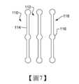
在圖6的例子中,遮罩體結構包括限定開口112的導電層110。由天線發射的無線信號可以穿過導電層110中限定的開口112。然而,導電層110的剩餘部分可以與發射電極104、感測電極106、在發射電極和感測電極之間的互電容交叉點108、觸摸感測器的其它部分或它們的組合重疊。在所示的例子中,導電層110包括與發射電極104對準的窄截面寬度114。在遮罩體結構的與互電容交叉點108重疊的區域處,導電層110包括形成圖案化遮罩區域116的寬度和區域,以在互電容交叉點處提供更有效的遮罩。在該例子中,圖案化遮罩區域116由窄截面寬度114沿垂直列118電連接。In the example of FIG. 6 , the mask structure includes a
圖7是描繪具有在互電容交叉點處重疊的窄截面寬度114和圖案化遮罩區域116的導電層110的例子。開口112由垂直列118之間的空間限定。在該特定例子中,感測器電極的部分未被導電層110的一部分遮罩。FIG. 7 depicts an example of a
在圖8的例子中,圖案化遮罩區域116徑向與附加的窄截面寬度114連接,這些寬度與感測電極重疊以形成水平行120。在該例子中,開口位於垂直列118和水平行120之間。在一些例子中,徑向連接垂直列可以使感應電流最小和/或減少為某些類型的天線發送無線信號所需的電能。In the example of FIG. 8 , patterned
圖9描繪具有觸摸感測器102和遮罩體結構202的堆疊部200的截面圖。觸摸感測器102可以包括基板204。基板204可以是任何合適類型的基板,諸如印刷電路板、玻璃纖維、電絕緣材料、另一種類型的材料或它們的組合。第一組電極208可以沉積在基板204的第一側206上。第一組電極208可以是發射電極、感測電極或另一類型電極。第二組電極212可以沉積在基板204的與第一側206相對的第二側210上。第二組電極212可以是發射電極、感測電極或另一類型電極。在該例子中,第一組電極208和第二組電極212彼此正交。FIG. 9 depicts a cross-sectional view of a
電絕緣材料214可以與第二組電極212相鄰,並且導電材料216可以沉積在電絕緣材料214的與第二組電極212相對的遠側218上。Electrically insulating
導電材料216可以遮罩觸摸感測器102的某些部分免受天線發射的射頻的影響。然而,導電材料216可以包括所有射頻穿過遮罩材料的開口220。
在圖9的例子中,導電材料216的與互電容交叉點重疊的寬度與第一組208中的電極一樣寬。然而,在圖10的例子中,導電材料216的寬度比電極的第一組208的寬度寬或者比互電容交叉點寬。導電材料的寬度可以取決於天線的調諧和/或其它電特性。然而,導電材料216的寬度也可以基於與天線的接近度而在整個觸摸感測器中變化。In the example of FIG. 9 , the width of the
在一些例子中,可以期望在更靠近天線的那些區域的導電材料中具有較大的開口。在這種區域中,導電材料216可以覆蓋較少的表面積,以允許開口更大,藉以為射頻通過提供更大的空間。在觸摸感測器的距離天線較遠的那些區域中,開口可以更小,導電材料216覆蓋更大的觸摸感測器表面積。In some examples, it may be desirable to have larger openings in the conductive material in those areas closer to the antenna. In such regions, the
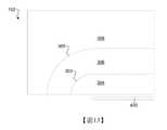
圖11描繪觸摸感測器102、第一天線300和第二天線302的例子。在該例子中,觸摸感測器102具有第一區域304、第二區域306和第三區域308。邊界區域303和305的虛線可以通常表示區域之間的邊界變化。第一區域304可以最靠近天線300、天線302,第二區域306可以次靠近天線300、302,並且第三區域308可以位於距天線300、302最遠的位置。在該例子中,第一區域304的遮罩材料中的開口可以大於其它區域中的開口,因此,遮罩材料可以覆蓋第一區域304中的較小的總表面積。在第二區域306中,遮罩材料可以覆蓋增加的表面積,藉以使得開口更小。在第三區域308中,開口可以是最小的,藉以與第二區域306中的開口相比,遮罩材料甚至覆蓋更多的表面積。在某些情況下,第三區域308中的遮罩材料可以覆蓋所有表面積而不提供開口。遮罩材料可以是結合圖3至圖10的實施例描述的導電層。FIG. 11 depicts an example of
圖12描繪在觸摸感測器102的邊緣處的邊界變化曲線的例子。在該例子中,邊界變化可以位於距天線的表面或天線的有源部分預設距離處。在該例子中,天線的端部未達到觸摸感測器102的端部,藉以允許觸摸感測器102的第二區域306和第三區域308具有更大的面積。FIG. 12 depicts an example of a boundary profile at the edge of the
在圖13的例子中,僅描繪與觸摸感測器102相鄰的單個天線400。在該例子中,天線400位於沿觸摸感測器102的長度的部分處。在該例子中,第一區域304的邊界可以減小,而第二區域306和第三區域308的區域可以增大。In the example of FIG. 13 , only a
觸摸感測器102可以包括具有不同數量的遮罩材料的任意合適數量的區域。例如,圖14描繪觸摸感測器102可以包括多於四個的區域304、306、308、310,但是在其它實施例中包括更多的區域。在一些例子中,可以僅存在具有不同數量遮罩體的兩個區域。
此外,具有不同數量的遮罩體的那些區域的幾何形狀可以具有不同的表面積。在圖15的例子中,區域之間的邊界區域303、305是不規則的。在該例子中,邊界區域303、305可以被成型為適應每個天線的不同特性。例如,根據第一天線300的電特性,可以期望第一區域304具有更大的面積,而由於第二天線的電特性,可以期望第一區域304具有更小的面積。因此,不同區域的幾何形狀可以包括在觸摸感測器102的一側上具有比另一側上更小的面積。Furthermore, the geometries of those regions with different numbers of mask volumes may have different surface areas. In the example of Fig. 15, the
圖16描繪,根據第一天線300的電特性,遮罩體的數量包括具有較少遮罩體的較大區域,但是更快速地過渡至具有更多遮罩體的第二區域306的例子。另一方面,第二天線302的電特性可以期望具有靠近第二天線的較少遮罩體的較小面積,並且具有更長的到遮罩體中沒有開口的區域的過渡區域。雖然這些例子描繪了具有遮罩體數量不同的特定配置的觸摸感測器,但是根據本文所描述的原理,可以使用遮罩體數量不同的區域的不同尺寸和幾何形狀的任何佈置。Figure 16 depicts an example where the number of shrouds includes a larger area with fewer shrouds, but transitions more quickly to a
圖17描繪發射信號的方法1700的例子。該方法1700可以基於圖1至圖16所描述的裝置、模組和原理來執行。在該例子中,方法17包括通過觸摸感測器的遮罩體結構發射1702無線信號,其中該遮罩體結構包括導電層中的至少一個開口,該開口大到足以使無線信號通過。17 depicts an example of a
在一些例子中,無線信號是WiFi信號、藍牙信號、近場通信信號、具有另一射頻的無線信號或它們的組合。具有觸控板的裝置可以是膝上型電腦、臺式電腦、用於向計算裝置或雲計算裝置提供輸入的外部板、計算裝置、聯網裝置、電子平板、移動設備、個人數位助理、控制台、遊戲裝置、平板、顯示器、電視、另一種類型的設備或它們的組合。In some examples, the wireless signal is a WiFi signal, a Bluetooth signal, a near field communication signal, a wireless signal with another radio frequency, or a combination thereof. A device having a touchpad can be a laptop computer, a desktop computer, an external board for providing input to a computing device or a cloud computing device, a computing device, a networked device, an electronic tablet, a mobile device, a personal digital assistant, a console , gaming console, tablet, monitor, television, another type of device, or a combination thereof.
應當注意的是,以上討論的方法、系統和設備僅旨在作為例子。必須強調的是,各種實施例可以適當地省略、替代或添加各種過程或元件。例如,應當理解的是,在替代實施例中,可以以與所描述的順序不同的循序執行所述方法,並且可以添加、省略或組合各個步驟。而且,關於某些實施例描述的特徵可以在各種其它實施例中組合。實施例的不同方面和元件可以以類似方式組合。而且,應當強調的是,技術在發展,因此,許多元件本質上是例子性的,不應解釋為限制本發明的範圍。It should be noted that the methods, systems and devices discussed above are intended to be examples only. It must be emphasized that various embodiments may omit, substitute or add various procedures or elements as appropriate. For example, it should be appreciated that in alternative embodiments, the methods may be performed in an order different from that described, and that various steps may be added, omitted, or combined. Furthermore, features described with respect to certain embodiments may be combined in various other embodiments. Different aspects and elements of the embodiments may be combined in a similar manner. Also, it should be emphasized that technology evolves and thus many of the elements are exemplary in nature and should not be construed as limiting the scope of the invention.
說明書中給出了具體細節以提供對實施例的透徹理解。然而,本領域的普通具有通常知識者將理解的是,可以在沒有這些具體細節的情況下實踐實施例。例如,在沒有不必要的細節的情況下已經示出了公知的電路、過程、演算法、結構和技術,以避免使實施例晦澀難懂。Specific details are given in the description to provide a thorough understanding of the embodiments. However, it will be understood by one of ordinary skill in the art that the embodiments may be practiced without these specific details. For example, well-known circuits, procedures, algorithms, structures and techniques have been shown without unnecessary detail in order not to obscure the embodiments.
另外,應當注意的是,實施例可以被描述為描繪流程圖或框圖的過程。儘管每個操作都可以被描述為順序過程,但是許多操作可以並行或同時執行。另外,可以重新排列操作的順序。一個過程可能具有圖中未包括的其它步驟。In addition, it should be noted that the embodiments may be described as depicting flowcharts or block diagramsprocess. Although each operation can be described as a sequential process, many operations can be performed in parallel or simultaneously. Additionally, the order of operations can be rearranged. A process may have other steps not included in the figure.
雖然描述了一些實施例,但本領域具有通常知識者將認識到的是,在不脫離本發明的精神的情況下,可以使用各種修改方案、替代方案以及等同方案。例如,以上元件可以僅是較大系統的元件,其中其它規則可以優先於或修改本發明的應用。同樣,在考慮以上元件之前、期間或之後可以採取許多步驟。因此,以上描述不應視為限制本發明的範圍。While some embodiments have been described, those having ordinary skill in the art will recognize that various modifications, substitutions, and equivalents can be used without departing from the spirit of the invention. For example, the above elements may only be elements of a larger system, where other rules may override or modify application of the present invention. Likewise, many steps may be taken before, during or after consideration of the above elements. Accordingly, the above description should not be taken as limiting the scope of the invention.
100:互電容感測裝置100: Mutual capacitance sensing device
10:觸控板10:Touchpad
12、121:行電極12, 121: row electrodes
14:列電極14: column electrode
16:觸摸控制器16: Touch controller
18:接地平面遮罩體18: Ground plane mask body
Claims (20)
Translated fromChineseApplications Claiming Priority (2)
| Application Number | Priority Date | Filing Date | Title |
|---|---|---|---|
| US201962794392P | 2019-01-18 | 2019-01-18 | |
| US62/794,392 | 2019-01-18 |
Publications (2)
| Publication Number | Publication Date |
|---|---|
| TW202107259A TW202107259A (en) | 2021-02-16 |
| TWI790413Btrue TWI790413B (en) | 2023-01-21 |
Family
ID=71678338
Family Applications (1)
| Application Number | Title | Priority Date | Filing Date |
|---|---|---|---|
| TW108147694ATWI790413B (en) | 2019-01-18 | 2019-12-25 | Shield for a capacitive touch system |
Country Status (2)
| Country | Link |
|---|---|
| CN (1) | CN111459342B (en) |
| TW (1) | TWI790413B (en) |
Citations (4)
| Publication number | Priority date | Publication date | Assignee | Title |
|---|---|---|---|---|
| US20140253830A1 (en)* | 2013-03-08 | 2014-09-11 | Wintek Corporation | Touch display apparatus |
| US20180032166A1 (en)* | 2015-02-10 | 2018-02-01 | Dexerials Corporation | Touch pad antenna device and electronic apparatus |
| US20180152549A1 (en)* | 2007-06-21 | 2018-05-31 | Apple Inc. | Handheld electronic device with cable grounding |
| CN108933329A (en)* | 2017-05-23 | 2018-12-04 | 苹果公司 | Antenna in patterned conductive layer |
Family Cites Families (5)
| Publication number | Priority date | Publication date | Assignee | Title |
|---|---|---|---|---|
| US7920129B2 (en)* | 2007-01-03 | 2011-04-05 | Apple Inc. | Double-sided touch-sensitive panel with shield and drive combined layer |
| JP5286228B2 (en)* | 2009-11-09 | 2013-09-11 | アルプス電気株式会社 | TOUCH PAD INPUT DEVICE WITH ANTENNA AND ELECTRONIC DEVICE HAVING THE DEVICE |
| JP5378243B2 (en)* | 2010-01-13 | 2013-12-25 | アルプス電気株式会社 | INPUT DEVICE WITH ANTENNA AND ELECTRONIC DEVICE PROVIDED WITH THE DEVICE |
| CN106102305A (en)* | 2016-06-30 | 2016-11-09 | 努比亚技术有限公司 | A kind of shielding construction and mobile terminal |
| CN106465556B (en)* | 2016-07-21 | 2019-01-18 | 北京小米移动软件有限公司 | Metal cap body and electronic equipment |
- 2019
- 2019-12-25TWTW108147694Apatent/TWI790413B/enactive
- 2020
- 2020-01-17CNCN202010050800.XApatent/CN111459342B/enactiveActive
Patent Citations (4)
| Publication number | Priority date | Publication date | Assignee | Title |
|---|---|---|---|---|
| US20180152549A1 (en)* | 2007-06-21 | 2018-05-31 | Apple Inc. | Handheld electronic device with cable grounding |
| US20140253830A1 (en)* | 2013-03-08 | 2014-09-11 | Wintek Corporation | Touch display apparatus |
| US20180032166A1 (en)* | 2015-02-10 | 2018-02-01 | Dexerials Corporation | Touch pad antenna device and electronic apparatus |
| CN108933329A (en)* | 2017-05-23 | 2018-12-04 | 苹果公司 | Antenna in patterned conductive layer |
Also Published As
| Publication number | Publication date |
|---|---|
| CN111459342B (en) | 2024-08-16 |
| TW202107259A (en) | 2021-02-16 |
| CN111459342A (en) | 2020-07-28 |
Similar Documents
| Publication | Publication Date | Title |
|---|---|---|
| US11281340B2 (en) | Radio frequency transparent capacitive touch systems and methods | |
| US20120329524A1 (en) | Touch sensor and antenna integration along an electronic device housing | |
| CN1295581C (en) | Laptop computer touchpad with integrated antenna | |
| US20160188092A1 (en) | Touchscreen antenna system and design method thereof | |
| US8743086B2 (en) | Dual-mode touch sensing apparatus | |
| CN106104913B (en) | Induction screen, control circuit and control method thereof and induction screen device | |
| US20170371473A1 (en) | Touch Sensor Device and Method | |
| CN113454581B (en) | Touch substrate and display device | |
| KR101706834B1 (en) | Touch panel and a manufacturing method thereof | |
| US20080110739A1 (en) | Touch-sensor device having electronic component situated at least partially within sensor element perimeter | |
| TWI758606B (en) | Antenna apparatus and electronic apparatus | |
| US12224489B2 (en) | Antenna shielding in a capacitance module | |
| WO2019228023A1 (en) | Touch substrate, display device and method for acquiring touch coordinates | |
| US20220350430A1 (en) | Touchpad Stack with an Antenna Layer | |
| US20220155893A1 (en) | Shield for a Capacitive Touch System | |
| WO2021233283A1 (en) | Electronic device | |
| US11994761B2 (en) | Ground feature in a capacitive touch system | |
| US20130240341A1 (en) | Touch panel | |
| TWI790413B (en) | Shield for a capacitive touch system | |
| US10983628B2 (en) | Touch module, a method for fabricating the same, and a touch display device | |
| US11620027B1 (en) | Thermal expansion groove of a capacitive touch system | |
| US11983373B1 (en) | Filter in a capacitance measuring circuit | |
| CN102200868A (en) | Antenna Loop Architecture with Capacitive Sensing and Electromagnetic Sensing Functions | |
| US20240012524A1 (en) | Antenna in a Capacitance Module | |
| CN111709212A (en) | Circuit board and layout method thereof, and terminal equipment |