TWI789853B - Radar apparatus and interference suppression method - Google Patents
Radar apparatus and interference suppression methodDownload PDFInfo
- Publication number
- TWI789853B TWI789853BTW110127877ATW110127877ATWI789853BTW I789853 BTWI789853 BTW I789853BTW 110127877 ATW110127877 ATW 110127877ATW 110127877 ATW110127877 ATW 110127877ATW I789853 BTWI789853 BTW I789853B
- Authority
- TW
- Taiwan
- Prior art keywords
- frequency
- signal
- error
- sampling
- digital signal
- Prior art date
Links
- 230000001629suppressionEffects0.000titleclaimsabstractdescription18
- 238000000034methodMethods0.000titleclaimsabstractdescription17
- 238000005070samplingMethods0.000claimsabstractdescription79
- 238000001914filtrationMethods0.000claimsdescription6
- 238000012545processingMethods0.000claimsdescription4
- 230000002452interceptive effectEffects0.000claims1
- 238000010586diagramMethods0.000description19
- 230000002238attenuated effectEffects0.000description3
- 230000010355oscillationEffects0.000description3
- 230000005611electricityEffects0.000description2
- 230000001934delayEffects0.000description1
- 238000001514detection methodMethods0.000description1
- 238000011161developmentMethods0.000description1
- 230000000694effectsEffects0.000description1
- 238000005259measurementMethods0.000description1
- 238000012986modificationMethods0.000description1
- 230000004048modificationEffects0.000description1
- 230000000737periodic effectEffects0.000description1
- 238000012876topographyMethods0.000description1
Images


Classifications
- G—PHYSICS
- G01—MEASURING; TESTING
- G01S—RADIO DIRECTION-FINDING; RADIO NAVIGATION; DETERMINING DISTANCE OR VELOCITY BY USE OF RADIO WAVES; LOCATING OR PRESENCE-DETECTING BY USE OF THE REFLECTION OR RERADIATION OF RADIO WAVES; ANALOGOUS ARRANGEMENTS USING OTHER WAVES
- G01S13/00—Systems using the reflection or reradiation of radio waves, e.g. radar systems; Analogous systems using reflection or reradiation of waves whose nature or wavelength is irrelevant or unspecified
- G01S13/02—Systems using reflection of radio waves, e.g. primary radar systems; Analogous systems
- G01S13/06—Systems determining position data of a target
- G01S13/08—Systems for measuring distance only
- G01S13/32—Systems for measuring distance only using transmission of continuous waves, whether amplitude-, frequency-, or phase-modulated, or unmodulated
- G—PHYSICS
- G01—MEASURING; TESTING
- G01S—RADIO DIRECTION-FINDING; RADIO NAVIGATION; DETERMINING DISTANCE OR VELOCITY BY USE OF RADIO WAVES; LOCATING OR PRESENCE-DETECTING BY USE OF THE REFLECTION OR RERADIATION OF RADIO WAVES; ANALOGOUS ARRANGEMENTS USING OTHER WAVES
- G01S7/00—Details of systems according to groups G01S13/00, G01S15/00, G01S17/00
- G01S7/02—Details of systems according to groups G01S13/00, G01S15/00, G01S17/00 of systems according to group G01S13/00
- G01S7/023—Interference mitigation, e.g. reducing or avoiding non-intentional interference with other HF-transmitters, base station transmitters for mobile communication or other radar systems, e.g. using electro-magnetic interference [EMI] reduction techniques
- G—PHYSICS
- G01—MEASURING; TESTING
- G01S—RADIO DIRECTION-FINDING; RADIO NAVIGATION; DETERMINING DISTANCE OR VELOCITY BY USE OF RADIO WAVES; LOCATING OR PRESENCE-DETECTING BY USE OF THE REFLECTION OR RERADIATION OF RADIO WAVES; ANALOGOUS ARRANGEMENTS USING OTHER WAVES
- G01S7/00—Details of systems according to groups G01S13/00, G01S15/00, G01S17/00
- G01S7/02—Details of systems according to groups G01S13/00, G01S15/00, G01S17/00 of systems according to group G01S13/00
- G01S7/03—Details of HF subsystems specially adapted therefor, e.g. common to transmitter and receiver
- G—PHYSICS
- G01—MEASURING; TESTING
- G01S—RADIO DIRECTION-FINDING; RADIO NAVIGATION; DETERMINING DISTANCE OR VELOCITY BY USE OF RADIO WAVES; LOCATING OR PRESENCE-DETECTING BY USE OF THE REFLECTION OR RERADIATION OF RADIO WAVES; ANALOGOUS ARRANGEMENTS USING OTHER WAVES
- G01S7/00—Details of systems according to groups G01S13/00, G01S15/00, G01S17/00
- G01S7/02—Details of systems according to groups G01S13/00, G01S15/00, G01S17/00 of systems according to group G01S13/00
- G01S7/28—Details of pulse systems
- G01S7/2813—Means providing a modification of the radiation pattern for cancelling noise, clutter or interfering signals, e.g. side lobe suppression, side lobe blanking, null-steering arrays
- G—PHYSICS
- G01—MEASURING; TESTING
- G01S—RADIO DIRECTION-FINDING; RADIO NAVIGATION; DETERMINING DISTANCE OR VELOCITY BY USE OF RADIO WAVES; LOCATING OR PRESENCE-DETECTING BY USE OF THE REFLECTION OR RERADIATION OF RADIO WAVES; ANALOGOUS ARRANGEMENTS USING OTHER WAVES
- G01S7/00—Details of systems according to groups G01S13/00, G01S15/00, G01S17/00
- G01S7/02—Details of systems according to groups G01S13/00, G01S15/00, G01S17/00 of systems according to group G01S13/00
- G01S7/35—Details of non-pulse systems
Landscapes
- Engineering & Computer Science (AREA)
- Radar, Positioning & Navigation (AREA)
- Remote Sensing (AREA)
- Computer Networks & Wireless Communication (AREA)
- Physics & Mathematics (AREA)
- General Physics & Mathematics (AREA)
- Radar Systems Or Details Thereof (AREA)
Abstract
Description
Translated fromChinese本發明是有關於一種雷達技術,且特別是有關於一種本發明實施例的雷達裝置及干擾抑制方法。The present invention relates to a radar technology, and in particular to a radar device and an interference suppression method according to an embodiment of the present invention.
雷達技術已發展多年。依據發射訊號種類,雷達技術大致可分成脈衝雷達和連續波雷達兩大類。常規脈衝雷達發射周期性的高頻脈衝。而連續波雷達發射連續波信號。隨著科技快速發展,近年來,調頻連續波(Frequency Modulated Continuous Wave,FMCW)雷達已廣泛應用在多種領域。Radar technology has evolved over the years. According to the type of transmitted signal, radar technology can be roughly divided into two categories: pulse radar and continuous wave radar. Conventional pulse radars emit periodic high-frequency pulses. Continuous wave radar emits a continuous wave signal. With the rapid development of science and technology, frequency modulated continuous wave (Frequency Modulated Continuous Wave, FMCW) radar has been widely used in various fields in recent years.
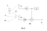
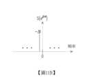
值得注意的是,雷達裝置經常受到外界干擾而影響目標物體的偵測結果。例如,圖1是連續波(CW)都卜勒(Doppler)雷達R的示意圖。請參照圖1,都卜勒雷達R的發射電路(如放大器PA)依據振盪器LO所提供的載波頻率將射頻訊號放大輸出,並透過傳送天線TA對外發射。所發射的訊號經物體O反射形成回波訊號SO。然而,無可避免地,環境中可能有諸如交流電(Alternating Current,AC)電力在50或60赫茲(Hz)及其諧波(harmonics)上的干擾或其他干擾。因此,不僅回波訊號SO,接收天線RA可能接收同通道(co-channel)干擾IC及鄰通道(adjacent-channel)干擾IAC。甚至,接收訊號經接收電路(如雜訊放大器LNA及混波器MIX)後還形成基頻或中頻干擾。It is worth noting that radar devices are often affected by external interference which affects the detection results of target objects. For example, FIG. 1 is a schematic diagram of a continuous wave (CW) Doppler radar R. As shown in FIG. Please refer to FIG. 1 , the transmitting circuit (such as the amplifier PA) of the Doppler radar R amplifies and outputs the radio frequency signal according to the carrier frequency provided by the oscillator LO, and transmits it externally through the transmitting antenna TA. The transmitted signal is reflected by the object O to form an echo signal SO. However, unavoidably, there may be conditions such as alternating current (AlternatingCurrent, AC) disturbances or other disturbances of electrical power at 50 or 60 hertz (Hz) and their harmonics. Therefore, not only the echo signal SO, but also the receiving antenna RA may receive co-channel interference IC and adjacent-channel interference IAC. Even, after the received signal passes through the receiving circuit (such as the noise amplifier LNA and the mixer MIX), it also forms base frequency or intermediate frequency interference.
本發明實施例的雷達裝置包括(但不僅限於)時脈產生器、類比至數位轉換器(Analog to Digital Converter,ADC)及陷波(notch)濾波器。時脈產生器用以產生取樣頻率。類比至數位轉換器耦接時脈產生器,並用以依據取樣頻率將類比訊號轉換成數位訊號。陷波濾波器耦接類比至數位轉換器,並用以衰減數位訊號中的一個或更多個受干擾頻率。這些受干擾頻率相關於取樣頻率。The radar device of the embodiment of the present invention includes (but not limited to) a clock generator, an analog to digital converter (Analog to Digital Converter, ADC) and a notch filter. The clock generator is used to generate the sampling frequency. The analog-to-digital converter is coupled to the clock generator and used for converting the analog signal into a digital signal according to the sampling frequency. The notch filter is coupled to the analog-to-digital converter and used to attenuate one or more disturbed frequencies in the digital signal. These disturbed frequencies are related to the sampling frequency.
另一方面,本發明實施例的干擾抑制方法適用於雷達裝置。干擾抑制方法包括(但不僅限於)下列步驟:產生取樣頻率。依據取樣頻率將類比訊號轉換成數位訊號。衰減數位訊號中的一個或更多個受干擾頻率。這些受干擾頻率相關於取樣頻率。On the other hand, the interference suppression method of the embodiment of the present invention is applicable to a radar device. The interference suppression method includes (but is not limited to) the following steps: generating a sampling frequency. Convert analog signal to digital signal according to sampling frequency. Attenuates one or more disturbed frequencies in a digital signal. These disturbed frequencies are related to the sampling frequency.
為讓本發明的上述特徵和優點能更明顯易懂,下文特舉實施例,並配合所附圖式作詳細說明如下。In order to make the above-mentioned features and advantages of the present invention more comprehensible, the following specific embodiments are described in detail together with the accompanying drawings.
R:都卜勒雷達R: Doppler Radar
PA:放大器PA: Amplifier
LO:振盪器LO: Oscillator
O:物體O: object
SO:回波訊號SO: echo signal
RA:接收天線RA: receiving antenna
IC:同通道干擾IC: co-channel interference
IAC:鄰通道干擾IAC: adjacent channel interference
MIX:混波器MIX: mixer
LNA:雜訊放大器LNA: Noise Amplifier
100:雷達裝置100: Radar device
110:時脈產生器110: Clock generator
120:取樣頻率鎖定迴路120: Sampling frequency locked loop
130:類比至數位轉換器130:Analog to Digital Converter
140:偏移估測器140: Offset Estimator
150:陷波濾波器150: Notch filter
SF:取樣頻率SF: sampling frequency
111:振盪器111: Oscillator
113:時脈除頻器113: clock frequency divider
fRC:振盪頻率fRC :Oscillation frequency
fε:頻率偏移fε : frequency offset
N:除頻倍數N: frequency division multiple
M:倍數M: multiple
fΛC、2fΛC、3fΛC:受干擾頻率fΛC , 2fΛC , 3fΛC : interfered frequencies
△f:頻率誤差△f: frequency error
x(n):數位訊號x(n): digital signal
y(n):訊號y(n): signal
xa(t):類比訊號xa (t): analog signal
Xa(f)、X(ej2πf)、V(ej2πf)、S(ej2πf):頻率響應Xa (f), X(ej2πf ), V(ej2πf ), S(ej2πf ): frequency response
151、153:加法器151, 153: adder
155:緩衝器155: buffer
157:頻寬選擇器157: Bandwidth selector
BW_sel:頻寬參數BW_sel: bandwidth parameter
△
170:偏移估測電路170: Offset estimation circuit
171:除頻濾波器171: frequency division filter
173:下混波器173: Down mixer
175:低通濾波器175: low pass filter
177:頻率估測器177: Frequency Estimator
v(n):基頻訊號v(n): fundamental frequency signal
s(n)、sI(n)、sQ(n):誤差訊號s(n), sI (n), sQ (n): error signal
S1、S2:序列S1, S2: sequence
731、732:混波器731, 732: Mixer
u(n)、u2:經濾波誤差訊號u(n), u2 : the filtered error signal
D:延遲D: delay
101:複數值101: complex value
103:實數值103: real value
S1510~S1550:步驟S1510~S1550: Steps
圖1是連續波都卜勒雷達的示意圖。Figure 1 is a schematic diagram of a continuous wave Doppler radar.
圖2是依據本發明一實施例的雷達裝置的元件方塊圖。FIG. 2 is a block diagram of components of a radar device according to an embodiment of the invention.
圖3是依據本發明一實施例的時脈產生器的元件方塊圖。FIG. 3 is a block diagram of components of a clock generator according to an embodiment of the invention.
圖4是依據本發明一實施例的類比訊號的頻率響應。FIG. 4 is a frequency response of an analog signal according to an embodiment of the present invention.
圖5是依據本發明一實施例的陷波濾波器的元件方塊圖。FIG. 5 is a block diagram of components of a notch filter according to an embodiment of the invention.
圖6是依據本發明一實施例的陷波濾波器的頻率響應。FIG. 6 is a frequency response of a notch filter according to an embodiment of the invention.
圖7是依據本發明一實施例的陷波濾波器的頻率響應的局部放大圖。FIG. 7 is a partial enlarged view of the frequency response of the notch filter according to an embodiment of the present invention.
圖8是依據本發明一實施例的(經頻率偏移)取樣訊號的頻率響應。FIG. 8 is a frequency response of a (frequency shifted) sampled signal according to an embodiment of the present invention.
圖9是依據本發明一實施例的偏移估測器的元件方塊圖。FIG. 9 is a block diagram of components of an offset estimator according to an embodiment of the invention.
圖10是依據本發明一實施例的基頻訊號的頻率響應。FIG. 10 is a frequency response of a baseband signal according to an embodiment of the present invention.
圖11A是依據本發明一實施例的下混波器的示意圖。FIG. 11A is a schematic diagram of a down-mixer according to an embodiment of the invention.
圖11B是依據本發明一實施例的誤差訊號的頻率響應。FIG. 11B is a frequency response of an error signal according to an embodiment of the present invention.
圖12是依據本發明一實施例的頻率估測器的等效示意圖。FIG. 12 is an equivalent schematic diagram of a frequency estimator according to an embodiment of the present invention.
圖13是依據本發明另一實施例的偏移估測器的元件方塊圖。FIG. 13 is a block diagram of components of an offset estimator according to another embodiment of the present invention.
圖14是依據本發明一實施例的頻率誤差對時間的示意圖。FIG. 14 is a schematic diagram of frequency error versus time according to an embodiment of the invention.
圖15是依據本發明一實施例的干擾抑制方法的流程圖。FIG. 15 is a flowchart of an interference suppression method according to an embodiment of the present invention.
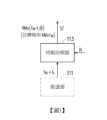
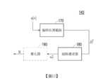
圖2是依據本發明一實施例的雷達裝置100的元件方塊圖。請參照圖2,雷達裝置100包括(但不僅限於)時脈產生器110、類比至數位轉換器130、及陷波濾波器150。雷達裝置100可應用於氣象、測速、倒車、地形、軍事等領域。雷達裝置100更可包括偏移估測器140,其中時脈產生器110、類比至數位轉換器130及偏移估測器140可形成一取樣頻率鎖定迴路(Sample Frequency Lock Loop,SFLL)120。請同時參照圖1,雷達裝置100更可包括發射電路(如放大器PA)依據振盪器LO所提供的載波頻率將射頻訊號放大輸出,並透過傳送天線TA對外發射,所發射的射頻訊號經物體O反射形成回波訊號SO,並經由接收電路(如雜訊放大器LNA及混波器MIX)接收後形成類比訊號xa(t)傳輸至類比至數位轉換器130。在一實施例中,雷達裝置100可為連續波(CW)都卜勒(Doppler)雷達,其中振盪器LO所提供的載波頻率為固定。FIG. 2 is a block diagram of components of a
時脈產生器110用於產生取樣頻率SF,以供類比至數位轉換器130所用。The
圖3是依據本發明一實施例的時脈產生器的元件方塊圖。請參照圖3,在一實施例中,時脈產生器110包括振盪器111及時脈除頻器113。振盪器111用以產生振盪頻率fRC(有時會伴隨著頻率偏移fε)的時脈訊號。時脈除頻器113耦接振盪器111,並用以依據除頻倍數N及振盪器111所提供的時脈訊號產生取樣頻率SF。即,對振盪頻率fRC除以除頻倍數N可得取樣頻率。FIG. 3 is a block diagram of components of a clock generator according to an embodiment of the invention. Referring to FIG. 3 , in one embodiment, the
取樣頻率SF的目標頻率為4M×fΛC,其中M為倍數,fΛC為受干擾頻率,並待後文詳述這目標頻率的決策。然而,若存在頻率偏移fε,則取樣頻率SF的實際頻率為4M×(fΛC+△f),其中△f為頻率誤差,並待後文詳述。The target frequency of the sampling frequency SF is 4M×fΛC , where M is a multiple, and fΛC is the interfered frequency, and the decision of the target frequency will be described in detail later. However, if there is a frequency offset fε , the actual frequency of the sampling frequency SF is 4M×(fΛC +Δf), where Δf is the frequency error, which will be described in detail later.
在另一實施例中,時脈產生器110包括時脈除頻器113,並透過外部的微控制器或RC振盪器提供時脈訊號。即,時脈產生器110可忽略振盪器111。In another embodiment, the
類比至數位轉換器130耦接時脈產生器110。在一實施例中,類比至數位轉換器130用以依據取樣頻率SF將類比訊號xa(t)轉換成數位訊號x(n)。這類比訊號xa(t)為雷達裝置100的回波訊號經混波的中頻訊號。類比至數位轉換器130對這中頻訊號(即,類比訊號xa(t))取樣,以將中頻訊號自連續時間域上的類比訊號轉換至離散時間域上的數位離散訊號(或是數位序列),也就是數位訊號x(n)。數位訊號x(n)可稱為雷達訊號100的基頻訊號。The analog-to-
值得注意的是,取樣頻率SF(或稱取樣率、取樣速度)是影響取樣結果的重要因素之一。假設取樣頻率SF為兩倍奈奎斯特(Nyquist)頻率。換句而言,奈奎斯特頻率為取樣頻率SF的一半。而為了抑制干擾,這取樣頻率SF進一步相關於所欲抑制的一個或更多個受干擾頻率。It is worth noting that the sampling frequency SF (or sampling rate, sampling speed) is one of the important factors affecting the sampling results. Assume that the sampling frequency SF is twice the Nyquist frequency. In other words, the Nyquist frequency is half of the sampling frequency SF. In order to suppress interference, the sampling frequency SF is further related to one or more interfered frequencies to be suppressed.
在一實施例中,取樣頻率SF為一個或更多個受干擾頻率中的基頻的整數倍。這整數倍可以是1、2、3、4、5或其他整數。在一實施例中,受干擾頻率包括基頻及基頻的一個或更多倍頻。In one embodiment, the sampling frequency SF is an integer multiple of the fundamental frequency of one or more interfered frequencies. This integer multiple can be 1, 2, 3, 4, 5 or other integers. In one embodiment, the interfered frequencies include the fundamental frequency and one or more multiples of the fundamental frequency.
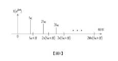
舉例而言,圖4是依據本發明一實施例的類比訊號xa(t)的頻率響應Xa(f)。請參照圖4,假設雷達裝置100所處位置受電力干擾。因此,電力所用頻率fΛC及其倍頻2fΛC(即,兩倍fΛC)、3fAC(即,三倍fΛC)會影響類比訊號xa(t)。若將電力的所用頻率fΛC作為受干擾頻率的基頻,則取樣頻率SF可以是4M×fΛC。由此可知,取樣頻率SF的大小相關於所涵蓋的受干擾頻率。然而,所涵蓋的受干擾頻率的基頻及其倍頻的數量仍可視實際需求而變更。For example, FIG. 4 is a frequency response Xa (f) of an analog signal xa (t) according to an embodiment of the present invention. Referring to FIG. 4 , it is assumed that the location of the
在一實施例中,這些受干擾頻率為已決定的,例如可以是電力所用的50或60赫茲(Hz)。在另一實施例中,受干擾頻率也可能是其他已決定的頻率,並視應用者的需求而可自行變更,本發明實施例不加以限制。In one embodiment, these interfered frequencies are determined, for example, 50 or 60 hertz (Hz) used by electricity. In another embodiment, the interfered frequency may also be other determined frequencies, which can be changed according to the requirements of the users, which is not limited by the embodiment of the present invention.
陷波濾波器150耦接類比至數位轉換器130。在一實施例中,在陷波濾波器150的陷波頻率範圍,陷波濾波器150用以衰減數位訊號x(n)中的一個或更多個受干擾頻率,以達到阻礙這受干擾頻率中的部分或全部通過的效果。換句而言,雷達裝置100將干擾頻率落在陷波濾波器150的陷波頻率範圍上。The
舉例而言,圖5是依據本發明一實施例的陷波濾波器150的元件方塊圖。請參照圖5,陷波濾波器150包括加法器151,153、緩衝器155及頻寬選擇器157。For example, FIG. 5 is a block diagram of components of a
加法器151用以將緩衝器155的輸出與數位訊號x(n)相加,並與緩衝器155的輸出經頻寬選擇器157的輸出相減。加法器153用以將加法器151的輸出與緩衝器155的輸出相減。緩衝器155為一分接延遲線(tapped delay-line)並提供一個或更多個延遲D用以暫存數位訊號x(n)中的4M個離散訊號。此時,取樣頻率SF為受干擾頻率的基頻的4M倍,且M為正整數。頻寬選擇器157用以改變受衰減的頻率的頻寬參數BW_sel。The
圖5所示的電路圖等效於:
圖6是依據本發明一實施例的陷波濾波器150的頻率響應。請參照圖6,假設奈奎斯特頻率為取樣頻率SF的一半,並忽略頻率誤差△f。即,2M×fΛC。因此,陷波濾波器150可衰減受干擾頻率fΛC、2fΛC、...、(2M-1)fΛC及2M×fΛC。FIG. 6 is a frequency response of the
在一實施例中,陷波濾波器150可決定受干擾頻率的數量。這數量與暫存緩衝器155中的離散訊號的數量有關。如圖6所示的數量為2M。須說明的是,緩衝器155所暫存的數量仍可視實際需求而變更,本發明實施例不加以限制。In one embodiment, the
圖7是依據本發明一實施例的陷波濾波器150的頻率響應的局部放大圖。請參照圖7,針對任一個受干擾頻率,頻寬參數BW_sel可改變缺口的頻寬,也就是所衰減的頻率範圍(或稱陷波頻率範圍)。其中,頻寬參數BW_sel越小,則缺口的頻寬越大。頻寬參數BW_sel越大,則缺口的頻寬越小。FIG. 7 is a partial enlarged view of the frequency response of the
由此可知,本發明實施例將取樣頻率相關於受干擾頻率,並衰減在離散時間域上對受干擾頻率中的基頻及其倍頻(即,諧波),即可有效抑制受干擾頻率。It can be seen that the embodiment of the present invention relates the sampling frequency to the interfered frequency, and attenuates the fundamental frequency and its multiplier (ie, harmonics) of the interfered frequency in the discrete time domain, so that the interfered frequency can be effectively suppressed. .
在一些情境中,取樣頻率SF可能受時脈產生器110的影響(例如,頻率偏移fε)而形成頻率誤差△f。圖8是依據本發明一實施例的(經頻率偏移fε)取樣訊號SF的頻率響應X(ej2πf)。請參照圖8,假設取樣頻率SF的目標頻率為4M×fΛC,但實際頻率卻是4M×(fΛC+△f)。與受干擾頻率fΛC、2fΛC、...、(2M-1)fΛC及2M×fΛC相比有偏差。此外,陷波濾波器150是依據實際取樣頻率來衰減訊號,若取樣頻率SF因頻率偏移而形成頻率誤差△f,將可能使得特定頻率的部分干擾或全部干擾無法抑制。因此,需要對取樣頻率SF校正,以提升抑制能力。In some situations, the sampling frequency SF may be affected by the clock generator 110 (eg, frequency offset fε ) to form a frequency error Δf. FIG. 8 shows the frequency response X(ej2πf ) of the sampled signal SF (shifted by fε ) according to an embodiment of the present invention. Referring to FIG. 8 , it is assumed that the target frequency of the sampling frequency SF is 4M×fΛC , but the actual frequency is 4M×(fΛC +Δf). There are deviations from the interfered frequencies fΛC , 2fΛC , . . . , (2M-1)fΛC and 2M×fΛC . In addition, the
請參照圖2,如先前所述,在一實施例中,除了時脈產生器110、類比至數位轉換器130及陷波濾波器150,雷達裝置100更可包括偏移估測器140。偏移估測器140耦接類比至數位轉換器130及時脈產生器110。偏移估測器140用以依據數位訊號x(n)估測頻率誤差△f(即,取得估測的頻率誤差△

圖9是依據本發明一實施例的偏移估測器140的元件方塊圖。請參照圖9,偏移估測器140可包括偏移估測電路170,偏移估測電路170可包括(但不僅限於)除頻(Decimation)濾波器171、下(down)混波器173、低通濾波器175及頻率估測器177。FIG. 9 is a block diagram of components of the offset
除頻(Decimation)濾波器171用以接收數位訊號x(n),並進行除頻處理以保留數位訊號x(n)中對應於基頻(fΛC+△f)的基頻訊號v(n)。即,對取樣頻率SF的實際頻率除以倍數M。
圖10是依據本發明一實施例的基頻訊號v(n)的頻率響應V(ej2πf)。請參照圖10,此時,奈奎斯特頻率為2(fΛC+△f),且基頻訊號v(n)僅有受干擾頻率fΛC。FIG. 10 is a frequency response V(ej2πf ) of the fundamental frequency signal v(n) according to an embodiment of the present invention. Please refer to FIG. 10 , at this time, the Nyquist frequency is 2(fΛC + Δf), and the baseband signal v(n) only has the disturbed frequency fΛC .
下混波器173耦接除頻濾波器171,並用以依據基頻訊號v(n)產生對應於頻率誤差△f的誤差訊號s(n)。即,對基頻訊號v(n)降頻。The down-
圖11A是依據本發明一實施例的下混波器173的示意圖。請參照圖11A,下混波器173透過混波器731,732對基頻訊號v(n)分別使用序列S1及S2混波。假設序列S1為{+1,0,-1,0,+1,0,-1,0,…},且序列S2為{0,-1,0,+1,0,-1,0,+1,…}。藉此,下混波器173可輸出同相的誤差訊號sI(n)及正交的誤差訊號sQ(n)。其中,誤差訊號s(n)為sI(n)+sQ(n)。須說明的是,在其他實施例中,序列S1及S2可能是其他相互正交的序列。FIG. 11A is a schematic diagram of the down-
圖11B是依據本發明一實施例的誤差訊號s(n)的頻率響應S(ej2πf)。請參照圖11B,誤差訊號s(n)在頻域上在負值的頻率誤差△f有值。FIG. 11B is a frequency response S(ej2πf ) of the error signal s(n) according to an embodiment of the present invention. Please refer to FIG. 11B , the error signal s(n) has a value at a negative frequency error Δf in the frequency domain.
低通濾波器175耦接下混波器173。在一實施例中,低通濾波器175用以對誤差訊號s(n)濾波,以產生經濾波誤差訊號u(n)。低通濾波器175可僅保留特定頻寬內的頻率響應,並據以僅保留在頻域上負值的頻率誤差△f的值。The low-
頻率估測器177耦接低通濾波器175。在一實施例中,頻率估測器177用以估測經濾波誤差訊號u(n)的頻率,以得出頻率誤差△f。頻率估測器177依據所估測的經濾波誤差訊號u(n)的頻率即可得出頻率誤差△f。The
假設經濾波誤差訊號u(n)的數學表示式為:

依據式子(3),圖12是依據本發明一實施例的頻率估測器177的等效示意圖。請參照圖12,頻率估測器177對經濾波誤差訊號u(n)分別取共軛(圖式為(.)*)及延遲D,並對兩輸出相乘取實數(圖式為Re(.)),以輸出Re{u*(n).u(n-1)}。另一方面,頻率估測器177對經濾波誤差訊號u(n)的平方取倒數(圖式為1/∥˙∥2),以輸出1/∥u(n)∥^2。以此分界,圖面左側為複數值101,且圖面右側為實數值103。頻率估測器177相乘兩輸出(Re{u*(n).u(n-1)}及1/∥u(n)∥^2)即可得出2π(

圖13是依據本發明另一實施例的偏移估測器140的元件方塊圖。請參照圖13,在一實施例中,除了偏移估測電路170,偏移估測器140可更包括迴路濾波器(loop filter)180。迴路濾波器180耦接偏移估測電路170,並用以對估測的頻率誤差△
在另一實施例中,除了偏移估測電路170,偏移估測器140可更包括迴路濾波器180及量化器(quantizer)190兩者。量化器190耦接迴路濾波器180。量化器190用以對經濾波誤差訊號u2量化,以產生除頻倍數N,除頻倍數N可為整數。而時脈產生器110依據除頻倍數N調整取樣頻率SF,類比至數位轉換器130再依取樣數位訊號x(n)繼續估測的頻率誤差調整取樣頻率,如此形成取樣頻率鎖定迴路120。量化器(quantizer)190例如是Sigma-Delta(Σ△)量化器。In another embodiment, in addition to the offset
由於時脈產生器110已知估測的頻率誤差△

在一實施例中,無論頻率誤差△f的大小,陷波濾波器150可對數位訊號衰減那些受干擾頻率上的訊號,並據以輸出經干擾抑制的訊號y(n)。In one embodiment, regardless of the magnitude of the frequency error Δf, the
在另一實施例中,反應於頻率誤差△f大於誤差門檻值,陷波濾波器150可禁能而不衰減數位訊號中的那些受干擾頻率。而反應於頻率誤差△f未大於誤差門檻值,陷波濾波器150可衰減數位訊號中的那些受干擾頻率。In another embodiment, in response to the frequency error Δf being greater than the error threshold, the
圖15是依據本發明一實施例的干擾抑制方法的流程圖。請參照圖2及圖15,時脈產生器110產生取樣頻率SF(步驟S1510)。類比至數位轉換器130依據取樣頻率SF將類比訊號xa(t)轉換成數位訊號x(n)(步驟S1530)。偏移估測器140依據數位訊號x(n)中之干擾頻率估測頻率偏移以使時脈產生器110調整取樣頻率SF,使干擾頻率落在陷波濾波器150的陷波頻率範圍上(步驟S1540)。在陷波頻率範圍,陷波濾波器150衰減數位訊號x(n)中的一個或更多個受干擾頻率(步驟S1550)。FIG. 15 is a flowchart of an interference suppression method according to an embodiment of the present invention. Referring to FIG. 2 and FIG. 15, the
關於圖15中的各步驟的實施細節在前述的實施例及實施方式都有詳盡的說明,於此不再贅述。除了以電路的形式實施,本發明實施例的各步驟與實施細節亦可由處理單元以軟體的方式實施,本發明實施例並不加以限制。The implementation details of each step in FIG. 15 have been described in detail in the aforementioned embodiments and implementation manners, and will not be repeated here. In addition to being implemented in the form of circuits, the various steps and implementation details of the embodiments of the present invention can also be implemented by the processing unit in the form of software, which is not limited by the embodiments of the present invention.
綜上所述,在本發明實施例的雷達裝置及干擾抑制方法中,設定取樣頻率相關於受干擾頻率,並在離散時間域上抑制位於那些受干擾頻率上的離散訊號。藉此,可抑制特定頻率及其諧波的干擾。To sum up, in the radar device and the interference suppression method of the embodiments of the present invention, the sampling frequency is set to be related to the interfered frequencies, and the discrete signals located on those interfered frequencies are suppressed in the discrete time domain. In this way, the interference of specific frequencies and their harmonics can be suppressed.
雖然本發明已以實施例揭露如上,然其並非用以限定本發明,任何所屬技術領域中具有通常知識者,在不脫離本發明的精神和範圍內,當可作些許的更動與潤飾,故本發明的保護範圍當視後附的申請專利範圍所界定者為準。Although the present invention has been disclosed as above with the embodiments, it is not intended to limit the present invention.Within the spirit and scope, some changes and modifications can be made, so the protection scope of the present invention should be defined by the scope of the appended patent application.
100:雷達裝置100: Radar device
110:時脈產生器110: Clock generator
120:取樣頻率鎖定迴路120: Sampling frequency locked loop
130:類比至數位轉換器130:Analog to Digital Converter
140:偏移估測器140: Offset Estimator
150:陷波濾波器150: Notch filter
SF:取樣頻率SF: sampling frequency
x(n):數位訊號x(n): digital signal
xa(t):類比訊號xa (t): analog signal
△
y(n):訊號y(n): signal
N:除頻倍數N: frequency division multiple
Claims (20)
Translated fromChinesePriority Applications (3)
| Application Number | Priority Date | Filing Date | Title |
|---|---|---|---|
| TW110127877ATWI789853B (en) | 2021-07-29 | 2021-07-29 | Radar apparatus and interference suppression method |
| CN202111024479.9ACN115685075A (en) | 2021-07-29 | 2021-09-02 | Radar device and interference suppression method |
| US17/494,794US12253589B2 (en) | 2021-07-29 | 2021-10-05 | Radar apparatus and interference suppression method |
Applications Claiming Priority (1)
| Application Number | Priority Date | Filing Date | Title |
|---|---|---|---|
| TW110127877ATWI789853B (en) | 2021-07-29 | 2021-07-29 | Radar apparatus and interference suppression method |
Publications (2)
| Publication Number | Publication Date |
|---|---|
| TWI789853Btrue TWI789853B (en) | 2023-01-11 |
| TW202305397A TW202305397A (en) | 2023-02-01 |
Family
ID=85038703
Family Applications (1)
| Application Number | Title | Priority Date | Filing Date |
|---|---|---|---|
| TW110127877ATWI789853B (en) | 2021-07-29 | 2021-07-29 | Radar apparatus and interference suppression method |
Country Status (3)
| Country | Link |
|---|---|
| US (1) | US12253589B2 (en) |
| CN (1) | CN115685075A (en) |
| TW (1) | TWI789853B (en) |
Citations (6)
| Publication number | Priority date | Publication date | Assignee | Title |
|---|---|---|---|---|
| CN1596488A (en)* | 2001-09-28 | 2005-03-16 | 阿雷伊通讯有限公司 | Frequency dependent calibration of a wideband radio system using narrowband channels |
| WO2006080457A1 (en)* | 2005-01-28 | 2006-08-03 | Anritsu Corporation | Short pulse radar and control method thereof |
| WO2011142394A1 (en)* | 2010-05-13 | 2011-11-17 | 測位衛星技術株式会社 | Navigation signal transmitter, navigation signal transmission method, and position information provision device |
| CN102590829A (en)* | 2012-03-14 | 2012-07-18 | 西安电子科技大学 | Complete self-adaptive notch filter for satellite navigation system and notch filtering method of same |
| US20140327902A1 (en)* | 2011-12-01 | 2014-11-06 | Leica Geosystems Ag | Distance measuring device |
| CN110418975A (en)* | 2017-03-09 | 2019-11-05 | 古河电气工业株式会社 | Radar device and target position detection method of radar device |
Family Cites Families (14)
| Publication number | Priority date | Publication date | Assignee | Title |
|---|---|---|---|---|
| US3728725A (en)* | 1971-04-23 | 1973-04-17 | Gen Electric | Target display for pulse-echo return system |
| US5194871A (en)* | 1982-03-01 | 1993-03-16 | Western Atlas International, Inc. | System for simultaneously deriving position information from a plurality of satellite transmissions |
| US5254999A (en)* | 1993-01-22 | 1993-10-19 | Samsung Electronics Co., Ltd. | Video signal processor for radar system |
| JPH09261954A (en)* | 1996-03-25 | 1997-10-03 | Aiwa Co Ltd | Stabilizing power supply apparatus and receiver employing the apparatus |
| US6791458B2 (en)* | 2001-05-22 | 2004-09-14 | Hubbell Incorporated | Dual technology occupancy sensor and method for using the same |
| DE102005044724A1 (en)* | 2005-09-19 | 2007-03-22 | Endress + Hauser Gmbh + Co. Kg | Runtime measurement method for determining the distance |
| US9680498B2 (en)* | 2009-06-26 | 2017-06-13 | Syntropy Systems, Llc | Sampling/quantization converters |
| US10613205B2 (en)* | 2014-10-06 | 2020-04-07 | Analog Devices, Inc. | Systems and methods for ultrasound beamforming |
| US10637641B2 (en)* | 2015-09-05 | 2020-04-28 | Westerngeco L.L.C. | Electromagnetic wave pulse synchronization |
| US9791551B1 (en) | 2016-04-25 | 2017-10-17 | Uhnder, Inc. | Vehicular radar system with self-interference cancellation |
| US10181860B1 (en) | 2017-10-26 | 2019-01-15 | Analog Devices Global Unlimited Company | Reducing residue signals in analog-to-digital converters |
| EP3496274A1 (en) | 2017-12-05 | 2019-06-12 | Nxp B.V. | Successive approximation register (sar) analog-to-digital converter (adc), radar unit and method for improving harmonic distortion performance |
| US11009597B2 (en) | 2018-12-17 | 2021-05-18 | Xilinx, Inc. | Phase noise compensation in digital beamforming radar systems |
| JP2021089180A (en)* | 2019-12-03 | 2021-06-10 | 古野電気株式会社 | Target detection device and target detection method |
- 2021
- 2021-07-29TWTW110127877Apatent/TWI789853B/enactive
- 2021-09-02CNCN202111024479.9Apatent/CN115685075A/enactivePending
- 2021-10-05USUS17/494,794patent/US12253589B2/enactiveActive
Patent Citations (6)
| Publication number | Priority date | Publication date | Assignee | Title |
|---|---|---|---|---|
| CN1596488A (en)* | 2001-09-28 | 2005-03-16 | 阿雷伊通讯有限公司 | Frequency dependent calibration of a wideband radio system using narrowband channels |
| WO2006080457A1 (en)* | 2005-01-28 | 2006-08-03 | Anritsu Corporation | Short pulse radar and control method thereof |
| WO2011142394A1 (en)* | 2010-05-13 | 2011-11-17 | 測位衛星技術株式会社 | Navigation signal transmitter, navigation signal transmission method, and position information provision device |
| US20140327902A1 (en)* | 2011-12-01 | 2014-11-06 | Leica Geosystems Ag | Distance measuring device |
| CN102590829A (en)* | 2012-03-14 | 2012-07-18 | 西安电子科技大学 | Complete self-adaptive notch filter for satellite navigation system and notch filtering method of same |
| CN110418975A (en)* | 2017-03-09 | 2019-11-05 | 古河电气工业株式会社 | Radar device and target position detection method of radar device |
Also Published As
| Publication number | Publication date |
|---|---|
| CN115685075A (en) | 2023-02-03 |
| TW202305397A (en) | 2023-02-01 |
| US20230035632A1 (en) | 2023-02-02 |
| US12253589B2 (en) | 2025-03-18 |
Similar Documents
| Publication | Publication Date | Title |
|---|---|---|
| JP2751840B2 (en) | Signal detection device | |
| US8422971B2 (en) | Spur mitigation for wireless communication systems | |
| TWI685669B (en) | Radar apparatus and leakage correction method | |
| US20130028595A1 (en) | Frequency offset estimating method and frequency offset estimating apparatus | |
| US20150145568A1 (en) | Time-to-digital convertor-assisted phase-locked loop spur mitigation | |
| Melzer et al. | Real-time mitigation of short-range leakage in automotive FMCW radar transceivers | |
| CN113922887A (en) | Carrier synchronization method and system for spatial coherent optical communication 2PSK modulation signal | |
| KR100524326B1 (en) | Apparatus for extracting the I/Q Mismatch caused by Up-conversion of direct conversion low IF scheme, and System and Method for Direct Conversion Digital Quadrature Transmission | |
| KR102263783B1 (en) | System and method for frequency offset estimation, and receiver using system for frequency offset estimation | |
| JPH10173721A5 (en) | ||
| JPH10173721A (en) | Mqam signal demodulating method | |
| JP3610343B2 (en) | Spurious signal removal method for measuring receiver | |
| TWI789853B (en) | Radar apparatus and interference suppression method | |
| CN111913154B (en) | Magnetron radar receiving phase parameter word processing method | |
| TWI593242B (en) | Receiving circuit and associated method capable of estimating frequency offset | |
| RU2352063C1 (en) | Method of noises inhibition and device for its realisation | |
| US11743852B2 (en) | Phase measurements for high accuracy distance measurements | |
| US20160182066A1 (en) | Auto frequency control circuit and receiver | |
| Kurniawan et al. | Implementation of automatic I/Q imbalance correction for FMCW radar system | |
| Kim et al. | Low-spurious wideband DDS-based Ku-band chirp generator for short-range radar application | |
| Song et al. | A frequency offset estimation algorithm based on under-sampling for THz communication | |
| Pedross-Engel et al. | Self-jamming mitigation via coding for millimeter-wave imaging with direct conversion receivers | |
| US11005509B2 (en) | Active tone canceller | |
| CN113219503B (en) | Digital code phase resolution error smoothing method and satellite navigation receiver | |
| Boiko et al. | Study of the Influence of Changing Signal Propagation Conditions |