TWI788869B - High electron mobility transistor and composite substrate thereof - Google Patents
High electron mobility transistor and composite substrate thereofDownload PDFInfo
- Publication number
- TWI788869B TWI788869BTW110120492ATW110120492ATWI788869BTW I788869 BTWI788869 BTW I788869BTW 110120492 ATW110120492 ATW 110120492ATW 110120492 ATW110120492 ATW 110120492ATW I788869 BTWI788869 BTW I788869B
- Authority
- TW
- Taiwan
- Prior art keywords
- layer
- stress
- substrate
- silicon
- silicon germanium
- Prior art date
Links
- 239000000758substrateSubstances0.000titleclaimsabstractdescription108
- 239000002131composite materialSubstances0.000titleclaimsabstractdescription52
- 229910000577Silicon-germaniumInorganic materials0.000claimsabstractdescription120
- LEVVHYCKPQWKOP-UHFFFAOYSA-N[Si].[Ge]Chemical compound[Si].[Ge]LEVVHYCKPQWKOP-UHFFFAOYSA-N0.000claimsabstractdescription101
- XUIMIQQOPSSXEZ-UHFFFAOYSA-NSiliconChemical compound[Si]XUIMIQQOPSSXEZ-UHFFFAOYSA-N0.000claimsabstractdescription27
- 229910052710siliconInorganic materials0.000claimsabstractdescription27
- 239000010703siliconSubstances0.000claimsabstractdescription27
- 230000006911nucleationEffects0.000claimsabstractdescription17
- 238000010899nucleationMethods0.000claimsabstractdescription17
- 239000010410layerSubstances0.000claimsdescription282
- 229910052732germaniumInorganic materials0.000claimsdescription18
- 239000004065semiconductorSubstances0.000claimsdescription17
- GNPVGFCGXDBREM-UHFFFAOYSA-Ngermanium atomChemical compound[Ge]GNPVGFCGXDBREM-UHFFFAOYSA-N0.000claimsdescription14
- 239000012792core layerSubstances0.000claimsdescription10
- 239000000203mixtureSubstances0.000claimsdescription10
- 229910052785arsenicInorganic materials0.000claimsdescription6
- 239000013078crystalSubstances0.000claimsdescription5
- 150000001875compoundsChemical class0.000claimsdescription3
- 229910052594sapphireInorganic materials0.000claimsdescription3
- 239000010980sapphireSubstances0.000claimsdescription3
- HBMJWWWQQXIZIP-UHFFFAOYSA-Nsilicon carbideChemical compound[Si+]#[C-]HBMJWWWQQXIZIP-UHFFFAOYSA-N0.000claimsdescription3
- 229910052582BNInorganic materials0.000claimsdescription2
- PZNSFCLAULLKQX-UHFFFAOYSA-NBoron nitrideChemical compoundN#BPZNSFCLAULLKQX-UHFFFAOYSA-N0.000claimsdescription2
- RQNWIZPPADIBDY-UHFFFAOYSA-Narsenic atomChemical compound[As]RQNWIZPPADIBDY-UHFFFAOYSA-N0.000claimsdescription2
- QVGXLLKOCUKJST-UHFFFAOYSA-Natomic oxygenChemical compound[O]QVGXLLKOCUKJST-UHFFFAOYSA-N0.000claimsdescription2
- PMHQVHHXPFUNSP-UHFFFAOYSA-Mcopper(1+);methylsulfanylmethane;bromideChemical compoundBr[Cu].CSCPMHQVHHXPFUNSP-UHFFFAOYSA-M0.000claimsdescription2
- 229910003460diamondInorganic materials0.000claimsdescription2
- 239000010432diamondSubstances0.000claimsdescription2
- AJNVQOSZGJRYEI-UHFFFAOYSA-Ndigallium;oxygen(2-)Chemical compound[O-2].[O-2].[O-2].[Ga+3].[Ga+3]AJNVQOSZGJRYEI-UHFFFAOYSA-N0.000claimsdescription2
- 229910001195gallium oxideInorganic materials0.000claimsdescription2
- 239000012212insulatorSubstances0.000claimsdescription2
- 229910052760oxygenInorganic materials0.000claimsdescription2
- 239000001301oxygenSubstances0.000claimsdescription2
- 229910010271silicon carbideInorganic materials0.000claimsdescription2
- 230000004888barrier functionEffects0.000abstractdescription3
- 229910002601GaNInorganic materials0.000description17
- JMASRVWKEDWRBT-UHFFFAOYSA-NGallium nitrideChemical compound[Ga]#NJMASRVWKEDWRBT-UHFFFAOYSA-N0.000description14
- 125000004429atomChemical group0.000description9
- 239000000463materialSubstances0.000description8
- XEEYBQQBJWHFJM-UHFFFAOYSA-NIronChemical compound[Fe]XEEYBQQBJWHFJM-UHFFFAOYSA-N0.000description6
- RNQKDQAVIXDKAG-UHFFFAOYSA-Naluminum galliumChemical compound[Al].[Ga]RNQKDQAVIXDKAG-UHFFFAOYSA-N0.000description5
- FYYHWMGAXLPEAU-UHFFFAOYSA-NMagnesiumChemical compound[Mg]FYYHWMGAXLPEAU-UHFFFAOYSA-N0.000description4
- 229910052749magnesiumInorganic materials0.000description4
- 239000011777magnesiumSubstances0.000description4
- 238000004519manufacturing processMethods0.000description4
- 238000000034methodMethods0.000description4
- 125000004430oxygen atomChemical groupO*0.000description4
- 230000005533two-dimensional electron gasEffects0.000description4
- OKTJSMMVPCPJKN-UHFFFAOYSA-NCarbonChemical compound[C]OKTJSMMVPCPJKN-UHFFFAOYSA-N0.000description3
- 229910052782aluminiumInorganic materials0.000description3
- XAGFODPZIPBFFR-UHFFFAOYSA-NaluminiumChemical compound[Al]XAGFODPZIPBFFR-UHFFFAOYSA-N0.000description3
- 229910052799carbonInorganic materials0.000description3
- 238000005229chemical vapour depositionMethods0.000description3
- 230000000694effectsEffects0.000description3
- 229910052742ironInorganic materials0.000description3
- 230000008569processEffects0.000description3
- 229910052581Si3N4Inorganic materials0.000description2
- 238000005452bendingMethods0.000description2
- 238000005253claddingMethods0.000description2
- 229910052751metalInorganic materials0.000description2
- 239000002184metalSubstances0.000description2
- HQVNEWCFYHHQES-UHFFFAOYSA-Nsilicon nitrideChemical compoundN12[Si]34N5[Si]62N3[Si]51N64HQVNEWCFYHHQES-UHFFFAOYSA-N0.000description2
- 239000002210silicon-based materialSubstances0.000description2
- 229910018072Al 2 O 3Inorganic materials0.000description1
- PIGFYZPCRLYGLF-UHFFFAOYSA-NAluminum nitrideChemical compound[Al]#NPIGFYZPCRLYGLF-UHFFFAOYSA-N0.000description1
- 208000032750Device leakageDiseases0.000description1
- UFHFLCQGNIYNRP-UHFFFAOYSA-NHydrogenChemical compound[H][H]UFHFLCQGNIYNRP-UHFFFAOYSA-N0.000description1
- 229910004298SiO 2Inorganic materials0.000description1
- VYPSYNLAJGMNEJ-UHFFFAOYSA-NSilicium dioxideChemical compoundO=[Si]=OVYPSYNLAJGMNEJ-UHFFFAOYSA-N0.000description1
- 238000000137annealingMethods0.000description1
- 230000005540biological transmissionEffects0.000description1
- 230000002860competitive effectEffects0.000description1
- 238000011109contaminationMethods0.000description1
- 230000003247decreasing effectEffects0.000description1
- 230000007812deficiencyEffects0.000description1
- 238000000151depositionMethods0.000description1
- 230000008021depositionEffects0.000description1
- 239000002019doping agentSubstances0.000description1
- 230000005684electric fieldEffects0.000description1
- 238000012986modificationMethods0.000description1
- 230000004048modificationEffects0.000description1
- 150000004767nitridesChemical class0.000description1
- 230000003647oxidationEffects0.000description1
- 238000007254oxidation reactionMethods0.000description1
- TWNQGVIAIRXVLR-UHFFFAOYSA-Noxo(oxoalumanyloxy)alumaneChemical compoundO=[Al]O[Al]=OTWNQGVIAIRXVLR-UHFFFAOYSA-N0.000description1
- 238000000059patterningMethods0.000description1
- 238000000926separation methodMethods0.000description1
- 229910052814silicon oxideInorganic materials0.000description1
Images


Landscapes
- Bipolar Transistors (AREA)
- Insulated Gate Type Field-Effect Transistor (AREA)
Abstract
Description
Translated fromChinese本揭露係關於一種供磊晶成長的複合基板,特別是關於一種高電子遷移率電晶體的複合基板以及在其上形成的高電子遷移率電晶體。The present disclosure relates to a composite substrate for epitaxial growth, and in particular to a composite substrate for high electron mobility transistors and high electron mobility transistors formed thereon.
氮化鎵材料因為具有寬能隙、高臨界電場、高導熱率、高飽和電子速度、高頻傳輸能力以及元件體積小等特性,使得氮化鎵在高功率及高速電晶體的應用上被視為是相當理想的材料,尤其是在高電子遷移率電晶體(high electron mobility transistor,HEMT)等高頻元件或是發光二極體(LED)元件的應用上相當廣泛。Gallium nitride material is regarded as a high-power and high-speed transistor application because of its wide energy gap, high critical electric field, high thermal conductivity, high saturation electron velocity, high-frequency transmission capability, and small component size. As an ideal material, it is widely used in high-frequency components such as high electron mobility transistor (HEMT) or light-emitting diode (LED) components.
矽基板在價格成本上有其競爭優勢,因此將氮化鎵等III-V族半導體化合物成長在矽基板上的電路設計方案正在蓬勃地研究與發展。由於氮化鎵與矽基板在晶格常數與熱膨脹係數等性質差異過大,因此通常會在氮化鎵和矽基板之間設置緩衝層,來幫助氮化鎵成長在矽基板上,然而,緩衝層的使用並無法完全滿足高電子遷移率電晶體對於氮化鎵等III-V族半導體化合物的薄膜品質要求。Silicon substrates have competitive advantages in terms of price and cost. Therefore, the circuit design scheme of growing III-V semiconductor compounds such as gallium nitride on silicon substrates is being vigorously researched and developed. Due to the large difference in properties such as lattice constant and thermal expansion coefficient between gallium nitride and silicon substrate, a buffer layer is usually set between gallium nitride and silicon substrate to help gallium nitride grow on the silicon substrate. However, the buffer layer The use of high electron mobility transistors cannot fully meet the film quality requirements of III-V semiconductor compounds such as gallium nitride.
有鑑於此,有必要提供一種高電子遷移率電晶體的複合基板,以解決習知技術中存在的缺失。In view of this, it is necessary to provide a composite substrate of high electron mobility transistors to solve the deficiencies in the prior art.
根據本揭露一實施例,提供一種高電子遷移率電晶體的複合基板,包括基底、設置於基底上的應力調控矽鍺層、以及設置於應力調控矽鍺層上的應力傳遞矽層。According to an embodiment of the present disclosure, a composite substrate of a high electron mobility transistor is provided, including a substrate, a stress-regulating silicon-germanium layer disposed on the substrate, and a stress-transferring silicon layer disposed on the stress-modulating silicon-germanium layer.
根據本揭露一實施例,提供一種高電子遷移率電晶體,包括基底、設置於基底上的應力調控矽鍺層、設置於應力調控矽鍺層上的應力傳遞矽層、設置於應力傳遞矽層上的成核層、設置於成核層上的緩衝層、設置於緩衝層上的高電阻層,其具有的電阻率高於緩衝層的電阻率、設置於高電阻層上的通道層、設置於通道層上的電子提供層、設置於電子提供層上的覆蓋層、設置於覆蓋層上的閘極電極、以及分別設置於閘極電極的兩側,且位於通道層上的源極電極和汲極電極。According to an embodiment of the present disclosure, a high electron mobility transistor is provided, including a substrate, a stress-regulating silicon-germanium layer disposed on the substrate, a stress-transferring silicon layer disposed on the stress-regulating silicon-germanium layer, and a stress-transferring silicon layer disposed on the stress-modulating silicon-germanium layer. The nucleation layer on the nucleation layer, the buffer layer arranged on the nucleation layer, the high resistance layer arranged on the buffer layer, which has a resistivity higher than the resistivity of the buffer layer, the channel layer arranged on the high resistance layer, the An electron supply layer on the channel layer, a cover layer provided on the electron supply layer, a gate electrode provided on the cover layer, and a source electrode and a source electrode respectively provided on both sides of the gate electrode and located on the channel layer Drain electrode.
100:複合基板100: composite substrate
102:核心層102: core layer
104:介電層104: Dielectric layer
106:元件晶圓106: Component wafer
108:半導體層108: Semiconductor layer
110:基底110: base
112:第一摻雜漸變矽鍺層112: the first doped graded silicon germanium layer
113:第一超晶格結構113: The first superlattice structure
114:第二摻雜漸變矽鍺層114: the second doped graded silicon germanium layer
115:第二超晶格結構115: Second superlattice structure
120:應力調控矽鍺層120: Stress control silicon germanium layer
130:應力傳遞矽層130: Stress transfer silicon layer
140:應力漸變層140: Stress gradient layer
200:高電子遷移率電晶體200: High Electron Mobility Transistor
202:步驟202: Step
204:步驟204: step
206:步驟206: Step
210:成核層210: nucleation layer
220:緩衝層220: buffer layer
230:高電阻層230: high resistance layer
240:通道層240: channel layer
250:電子提供層250: electron providing layer
260:覆蓋層260: Overlay
270:閘極電極270: gate electrode
280:源極電極280: source electrode
290:汲極電極290: Drain electrode
2DEG:二維電子氣2DEG: two-dimensional electron gas
為讓本揭露的上述與其他目的、特徵及實施例能更明顯易懂,所附圖式之說明如下,此外,為了清楚起見,圖式中的各特徵可能未必按照實際的比例繪製,因此某些圖式中的部分特徵的尺寸可能被刻意放大或縮小。In order to make the above and other objects, features and embodiments of the present disclosure more comprehensible, the attached drawings are described as follows. In addition, for the sake of clarity, each feature in the drawings may not necessarily be drawn according to the actual scale, so The dimensions of some features in some drawings may be intentionally enlarged or reduced.
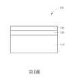
第1圖是根據本揭露一實施例所繪示的複合基板的剖面示意圖。FIG. 1 is a schematic cross-sectional view of a composite substrate according to an embodiment of the present disclosure.
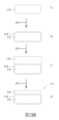
第2圖是根據本揭露一實施例所繪示的複合基板之基底的製造過程之剖面示意圖。FIG. 2 is a schematic cross-sectional view of the manufacturing process of the base of the composite substrate according to an embodiment of the present disclosure.
第3圖是根據本揭露另一實施例所繪示的複合基板的剖面示意圖。FIG. 3 is a schematic cross-sectional view of a composite substrate according to another embodiment of the disclosure.
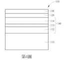
第4圖是根據本揭露另一實施例所繪示的複合基板的剖面示意圖。FIG. 4 is a schematic cross-sectional view of a composite substrate according to another embodiment of the disclosure.
第5圖是根據本揭露另一實施例所繪示的複合基板的剖面示意圖。FIG. 5 is a schematic cross-sectional view of a composite substrate according to another embodiment of the disclosure.
第6圖是根據本揭露另一實施例所繪示的複合基板的剖面示意圖。FIG. 6 is a schematic cross-sectional view of a composite substrate according to another embodiment of the disclosure.
第7圖是根據本揭露一實施例所繪示的高電子遷移率電晶體的剖面示意圖。FIG. 7 is a schematic cross-sectional view of a high electron mobility transistor according to an embodiment of the present disclosure.
為了使本揭示內容的敘述更加詳盡與完備,下文針對了本揭露的實施態樣與具體實施例提出了說明性的描述;但這並非實施或運用本發明具體實施例的唯一形式。實施方式中涵蓋了多個具體實施例的特徵以及用以建構與操作這些具體實施例的方法步驟與其順序。然而,亦可利用其他具體實施例來達成相同或均等的功能與步驟順序。In order to make the description of the present disclosure more detailed and complete, the following provides illustrative descriptions of the implementations and specific embodiments of the present disclosure; but this is not the only way to implement or use the specific embodiments of the present invention. The description covers features of various embodiments as well as method steps and their sequences for constructing and operating those embodiments. However, other embodiments can also be used to achieve the same or equivalent functions and step sequences.
以下描述的數值範圍與參數皆是約略的數值,在此處,「約」通常係指實際數值在一特定數值或範圍的正負10%、5%、1%或0.5%之內。當可理解此處所用的所有範圍、數量、數值、比例與百分比均經過「約」的修飾。因此,除非另有相反的說明,本說明書與附隨申請專利範圍所揭示的數值參數皆為約略的數值,且可視需求而更動。The numerical ranges and parameters described below are approximate numerical values. Here, "about" usually means that the actual numerical value is within plus or minus 10%, 5%, 1% or 0.5% of a specific numerical value or range. It should be understood that all ranges, amounts, values, ratios and percentages used herein are modified by "about". Therefore, unless otherwise stated to the contrary, the numerical parameters disclosed in this specification and the appended patent claims are approximate values and may be changed as required.
第1圖是根據本揭露一實施例所繪示的複合基板的剖面示意圖。如第1圖所示,複合基板100包含基底110,基底110可以是絕緣層上覆矽(silicon-on-insulator,SOI)基底、單晶半導體基底、多晶半導體基底、鑽石基底或藍寶石基底,其中單晶半導體基底或多晶半導體基底的材料可以是矽、氮化鋁、碳化矽、氧化鎵或氮化硼。基底110之矽材料可以是無摻雜的Si<111>、Si<110>或Si<100>,或是矽材料可摻雜例如鍺(Ge)、砷(As)、氧(O)原子或前述之組合,摻雜濃度例如為1x10¹³至1x10²⁰atom/cm-3。此外,複合基板100還包含應力調控矽鍺層120設置於基底110上,以及應力傳遞矽層130設置於應力調控矽鍺層120上。根據本揭露一些實施例,應力調控矽鍺層120的組成例如是Si1-x3Gex3,其中0<x3<1,且應力調控矽鍺層120中可摻雜例如Ge、As、O原子或前述之組合,摻雜濃度例如為1x1020atom/cm-3,應力調控矽鍺層120的厚度可以是0.1微米(μm)至10μm,應力傳遞矽層130的厚度可以是0.1μm至10μm,可以使用有機金屬化學氣相沉積法(metal-organic chemical vapor deposition,MOCVD)在同一製程腔室內形成應力調控矽鍺層120和應力傳遞矽層130。其中,為了順利在基底110的表面上磊晶成長應力調控矽鍺層120,可以在基底110和應力調控矽鍺層120之間額外設置具有特定晶面的半導體層,例如矽(111)。FIG. 1 is a schematic cross-sectional view of a composite substrate according to an embodiment of the present disclosure. As shown in FIG. 1, the
第2圖是根據本揭露一實施例所繪示的複合基板之基底110的製造過程之剖面示意圖。如第2(a)圖所示,首先提供核心層102,例如支撐晶圓(handle wafer),核心層102可以是矽、碳化矽(SiC)、藍寶石或其他硬度較大的基板,核心層102的厚度例如是300μm至1500μm。接著,經由步驟202,如第2(b)圖所示,在核心層102的表面形成介電層104,以作為後續晶圓鍵合的鍵合層(bonding layer),及/或用以增強基底整體的抗彎曲性或楊氏係數。其中,介電層104可以是氧化矽(SiO2)、氧化鋁(Al2O3)、氮化矽(SiN)或其他絕緣氧化物,介電層104的厚度可以是0.05μm至5μm,可以利用熱氧化或沉積的方式形成介電層104,並且介電層104可以包裹整個核心層102的正面、背面及側面。之後,經由步驟204,如第2(c)圖所示,提供元件晶圓106,將元件晶圓106鍵合(bonding)至介電層104上,並進行熱處理製程(annealing)。然後,經由步驟206,如第2(d)圖所示,將元件晶圓106減薄,繼以研磨減薄後的表面,得到半導體層108,並完成基底110的製造,其中,可以利用研磨(grinding)及化學機械研磨(chemical-mechanical planarization,CMP)方式進行步驟206,或是利用植入氫氣並膨脹產生微孔隙的分離方式(smart cut)以進行步驟206。同時參考第1圖和第2(d)圖,基底110的半導體層108設置於介電層104與應力調控矽鍺層120之間,半導體層108的厚度可以是0.1μm至10μm。根據本揭露之實施例,核心層102可以增加複合基板100之基底110的硬度,使得複合基板100抗翹曲(bending)效果得以提昇。此外,還可以利用介電層104的厚度調整來降低後續在複合基板100上磊晶成長的氮化鎵層之應力影響,改善基底110的彎曲(bowing)程度。FIG. 2 is a schematic cross-sectional view of the manufacturing process of the
第3圖是根據本揭露另一實施例所繪示的複合基板的剖面示意圖。第3圖與第2圖的差異在於第3圖的複合基板100之基底110與應力調控矽鍺層120之間額外設置有應力漸變層140,並且應力漸變層140的底部區域的鍺莫爾分率高於頂部區域的鍺莫爾分率。根據一實施例,如第3圖所示,應力漸變層140可包含位於底部區域的第一摻雜漸變矽鍺層112及位於頂部區域的第二摻雜漸變矽鍺層114。根據本揭露一些實施例,第一摻雜漸變矽鍺層112的組成例如是Si1-x1Gex1、第二摻雜漸變矽鍺層114的組成例如是Si1-x2Gex2,其中0<x3<x2<x1<1,且x3為應力調控矽鍺層120的Si1-x3Gex3中的鍺莫爾分率。第一摻雜漸變矽鍺層112和第二摻雜漸變矽鍺層114中可摻雜例如Ge、As、O原子或前述之組合,摻雜濃度例如為1x10²⁰atom/cm-3,第一摻雜漸變矽鍺層112和第二摻雜漸變矽鍺層114的厚度可以各自是0.1μm至20μm。由於第一摻雜漸變矽鍺層112的晶格常數會大於第二摻雜漸變矽鍺層114的晶格常數,因此可以在不影響應力傳遞矽層130和基底110之間的附著性的情況下,進一步提昇施加至應力傳遞矽層130和上方其他半導體層(圖未示)的張應力。FIG. 3 is a schematic cross-sectional view of a composite substrate according to another embodiment of the disclosure. The difference between FIG. 3 and FIG. 2 is that a
第4圖是根據本揭露另一實施例所繪示的複合基板的剖面示意圖。第4圖與第3圖的差異在於第4圖的複合基板100之第一摻雜漸變矽鍺層112與第二摻雜漸變矽鍺層114之間額外設置有第一超晶格結構113,此實施例之應力漸變層140包含第一摻雜漸變矽鍺層112、第一超晶格結構113及第二摻雜漸變矽鍺層114由下至上依序設置於基底110與應力調控矽鍺層120之間。第一超晶格結構113包含複數對成對堆疊的矽鍺層,每一對矽鍺層的組成與第一摻雜漸變矽鍺層112和第二摻雜漸變矽鍺層114的組成相同,例如是Si1-x1Gex1和Si1-x2Gex2,其中x1是第一摻雜漸變矽鍺層112的鍺莫爾分率,x2是第二摻雜漸變矽鍺層114的鍺莫爾分率,每一對矽鍺層的厚度小於第一摻雜漸變矽鍺層112和第二摻雜漸變矽鍺層114的厚度,例如可以是0.5nm至15nm,並且第一超晶格結構113可包含20對矽鍺層,第一超晶格結構113中可摻雜例如Ge、As、O原子或前述之組合,摻雜濃度例如為1x10²⁰atom/cm-3。FIG. 4 is a schematic cross-sectional view of a composite substrate according to another embodiment of the disclosure. The difference between FIG. 4 and FIG. 3 is that a
第5圖是根據本揭露另一實施例所繪示的複合基板的剖面示意圖。第5圖與第3圖的差異在於第5圖的複合基板100之第二摻雜漸變矽鍺層114與應力調控矽鍺層120之間額外設置有第二超晶格結構115,此實施例之應力漸變層140包含第一摻雜漸變矽鍺層112、第二摻雜漸變矽鍺層114及第二超晶格結構115由下至上依序設置於基底110與應力調控矽鍺層120之間。第二超晶格結構115包含複數對成對堆疊的矽鍺層,每一對矽鍺層的組成與第二摻雜漸變矽鍺層114和應力調控矽鍺層120的組成相同,例如是Si1-x2Gex2和Si1-x3Gex3,其中x2是第二摻雜漸變矽鍺層114的鍺莫爾分率,x3是應力調控矽鍺層120的鍺莫爾分率,每一對矽鍺層的厚度小於第一摻雜漸變矽鍺層112和第二摻雜漸變矽鍺層114的厚度,例如可以是0.5nm至15nm,並且第二超晶格結構115可包含20對矽鍺層,第二超晶格結構115中可摻雜例如是Ge、As、O原子或前述之組合,摻雜濃度例如為1x10²⁰atom/cm-3。此外,第5圖的複合基板100之應力傳遞矽層130的厚度可以是50nm至100nm。FIG. 5 is a schematic cross-sectional view of a composite substrate according to another embodiment of the disclosure. The difference between FIG. 5 and FIG. 3 is that a
第6圖是根據本揭露另一實施例所繪示的複合基板的剖面示意圖。第6圖與第3圖的差異在於第6圖的複合基板100之第一摻雜漸變矽鍺層112和第二摻雜漸變矽鍺層114之間額外設置有第一超晶格結構113,並且第二摻雜漸變矽鍺層114與應力調控矽鍺層120之間設置有第二超晶格結構115,此實施例之應力漸變層140包含第一摻雜漸變矽鍺層112、第一超晶格結構113、第二摻雜漸變矽鍺層114及第二超晶格結構115由下至上依序設置於基底110與應力調控矽鍺層120之間。在第6圖的複合基板100中,第一超晶格結構113和第二超晶格結構115的組成、摻雜元素、摻雜濃度及厚度可以參考前述第5圖和第6圖的複合基板100。FIG. 6 is a schematic cross-sectional view of a composite substrate according to another embodiment of the disclosure. The difference between FIG. 6 and FIG. 3 is that a
根據本揭露之實施例,在第一摻雜漸變矽鍺層112、第二摻雜漸變矽鍺層114、應力調控矽鍺層120之間插入第一超晶格結構113、第二超晶格結構115可以強化複合基板100的這些矽鍺層的磊晶品質,避免差排(dislocation)產生,並且可避免因為各矽鍺層之間的應力釋放而造成複合基板100的結構受損。According to an embodiment of the present disclosure, the
此外,可以使用有機金屬化學氣相沉積法(MOCVD)在同一製程腔室內形成前述實施例中的第一摻雜漸變矽鍺層112、第二摻雜漸變矽鍺層114、第一超晶格結構113、第二超晶格結構115、應力調控矽鍺層120和應力傳遞矽層130,因此可以改善製程效率,並避免這些層在製造過程受到污染。In addition, the first doped graded
第7圖是根據本揭露一實施例所繪示的高電子遷移率電晶體的剖面示意圖。如第7圖所示,高電子遷移率電晶體(HEMT)200包含成核層210設置在複合基板100上,複合基板100可以選自前述第1、3、4、5、6圖之複合基板100,為了簡化圖式,第7圖的複合基板100僅以一方塊繪示。成核層210設置在複合基板100的應力傳遞矽層130上,成核層210的材料例如是氮化鋁(AlN),並且可包含由下層的第一成核層和上層的第二成核層,第一成核層的厚度可以是30nm至80nm,成長溫度介於800至1000℃,第二成核層的厚度可以是30nm至200nm,成長溫度介於900至1100℃。HEMT 200還包含緩衝層220,例如是超晶格層,設置於成核層210上,緩衝層220的材料例如是氮化鋁鎵,並且可包含多層氮化鋁鎵層,例如5層氮化鋁鎵緩衝層,這些氮化鋁鎵緩衝層的鋁莫爾分率從下到上逐漸減少,每一層氮化鋁鎵緩衝層的厚度介於50nm至1000nm,成長溫度介於1000至1300℃。緩衝層220中可摻雜元素例如是碳、鐵、鎂或前述之組合,其中碳的摻雜濃度例如為1x10¹⁶至1x10²¹atom/cm-3,鐵或鎂的摻雜濃度例如為1x1016至1x1020atom/cm-3。HEMT 200還包含高電阻層230設置於緩衝層220上,高電阻層230的電阻率高於緩衝層220的電阻率,高電阻層230的材料例如是氮化鋁鎵,其鋁莫爾分率小於緩衝層220最頂層的鋁莫爾分率,高電阻層230的厚度可以是1600nm至2300nm,成長溫度介於1000至1300℃,高電阻層230中可摻雜元素例如是碳、鐵、鎂或前述之組合,其摻雜濃度範圍與緩衝層220相同。FIG. 7 is a schematic cross-sectional view of a high electron mobility transistor according to an embodiment of the present disclosure. As shown in FIG. 7, a high electron mobility transistor (HEMT) 200 including a
HEMT 200還包含通道層(channel layer)240,其設置於高電阻層230上,通道層240的材料例如是氮化鎵(GaN),厚度可以是0.2nm至1000nm,成長溫度介於1000至1300℃。電子提供層(barrier layer)250設置於通道層240上,電子提供層250的材料例如是氮化鋁鎵,厚度可以是10nm至30nm,成長溫度介於1000至1300℃。覆蓋層(cap layer)260設置於電子提供層250上,覆蓋層260可以是p型氮化鎵(GaN)層或p型氮化鋁鎵(AlGaN)層,其厚度可以分別為10nm至20nm、10nm至150nm,其中p型摻雜元素可以是鎂,摻雜濃度例如為1x10¹⁶至1x10²³atom/cm-3。HEMT 200的成核層210、緩衝層220、高電阻層230、通道層240、電子提供層250和覆蓋層260都可以經由有機金屬化學氣相沉積法(MOCVD)而磊晶成長形成。The
此外,HEMT 200還包含閘極電極270、源極電極280和汲極電極290。閘極電極27設置於覆蓋層260上,而源極電極280和汲極電極290分別設置於閘極電極270的兩側,且位於通道層240上,其中閘極電極270和覆蓋層260可以一起圖案化而形成,源極電極280和汲極電極290可以穿過電子提供層250到達通道層240的頂面,或者到達通道層240的一深度。如第7圖所示,未被覆蓋層260覆蓋的區域會因為通道層240和電子提供層250間所產生的壓電效應而形成二維電子氣(two dimensional electron gas)2DEG。利用閘極電極270向p型覆蓋層260施加偏壓,可以調控位於p型覆蓋層260下方的通道層240中的二維電子氣濃度,進而調控HEMT的開關。In addition, the
根據本揭露之實施例,複合基板100的基底110之核心層102為硬度較大的基底,可以提昇基底110抗翹曲的效果。此外,可以藉由基底110之介電層104的厚度調控來降低上方的磊晶層例如氮化鎵通道層240之應力影響,可以改善基底110的彎曲,因此複合基板100的基底110可以解決基板翹曲問題。另外,複合基板100的應力調控矽鍺層120的晶格較應力傳遞矽層130的晶格大,因此會對上方的氮化鎵通道層240產生張應力,讓通道層240的2DEG濃度增加,提高元件通道的電流量,進而提昇HEMT的電性效能。According to an embodiment of the present disclosure, the
另外,根據本揭露之實施例,當應力漸變層140的鍺莫爾分率從頂部區域到底部區域逐漸增加時,應力漸變層140的晶格常數也會從頂部區域到底部區域逐漸增加,使得應力漸變層140的晶格從上至下逐漸變大,藉由應力漸變層140的第一摻雜漸變矽鍺層112和第二摻雜漸變矽鍺層114的組成漸變來調整晶格大小,使得上方的氮化鎵通道層240所受張應力增加,可以進一步提高通道層240中的二維電子氣濃度,進而提高元件通道的電流量。相較於氮化鎵磊晶層形成在矽基板上之HEMT,本揭露之實施例可以讓通道層240之2DEG濃度大幅增加約3倍,並且相較於氮化鎵磊晶層形成在SOI基板上之HEMT,本揭露之實施例可以讓通道層240之2DEG濃度大幅增加約26倍。In addition, according to an embodiment of the present disclosure, when the germanium mole fraction of the
此外,根據本揭露之實施例,第一超晶格結構113和第二超晶格結構115的設置可以避免差排(dislocation)產生,而可以強化第一摻雜漸變矽鍺層112、第二摻雜漸變矽鍺層114和應力調控矽鍺層120的磊晶品質,並且避免因為各矽鍺層之間的應力釋放而造成複合基板100的結構受損。另外,本揭露之實施例可以讓HEMT的整體磊晶結構之厚度超過10μm,有效降低元件漏電,改善HEMT在高電壓操作下的效能和可靠度。In addition, according to the embodiment of the present disclosure, the arrangement of the
以上所述僅為本發明之較佳實施例,凡依本發明申請專利範圍所做之均等變化與修飾,皆應屬本發明之涵蓋範圍。The above descriptions are only preferred embodiments of the present invention, and all equivalent changes and modifications made according to the scope of the patent application of the present invention shall fall within the scope of the present invention.
100:複合基板100: composite substrate
110:基底110: base
112:第一摻雜漸變矽鍺層112: the first doped graded silicon germanium layer
114:第二摻雜漸變矽鍺層114: the second doped graded silicon germanium layer
120:應力調控矽鍺層120: Stress control silicon germanium layer
130:應力傳遞矽層130: Stress transfer silicon layer
140:應力漸變層140: Stress gradient layer
Claims (11)
Translated fromChinesePriority Applications (1)
| Application Number | Priority Date | Filing Date | Title |
|---|---|---|---|
| TW110120492ATWI788869B (en) | 2021-06-04 | 2021-06-04 | High electron mobility transistor and composite substrate thereof |
Applications Claiming Priority (1)
| Application Number | Priority Date | Filing Date | Title |
|---|---|---|---|
| TW110120492ATWI788869B (en) | 2021-06-04 | 2021-06-04 | High electron mobility transistor and composite substrate thereof |
Publications (2)
| Publication Number | Publication Date |
|---|---|
| TW202248479A TW202248479A (en) | 2022-12-16 |
| TWI788869Btrue TWI788869B (en) | 2023-01-01 |
Family
ID=85793485
Family Applications (1)
| Application Number | Title | Priority Date | Filing Date |
|---|---|---|---|
| TW110120492ATWI788869B (en) | 2021-06-04 | 2021-06-04 | High electron mobility transistor and composite substrate thereof |
Country Status (1)
| Country | Link |
|---|---|
| TW (1) | TWI788869B (en) |
Citations (2)
| Publication number | Priority date | Publication date | Assignee | Title |
|---|---|---|---|---|
| TW521395B (en)* | 2000-10-19 | 2003-02-21 | Ibm | A method of preparing a relaxed SiGe layer on an insulator and a SiGe/Si heterostructure and a multiple layer substrate using the method to form |
| JP4296727B2 (en)* | 2001-07-06 | 2009-07-15 | 株式会社Sumco | Semiconductor substrate, field effect transistor, method of forming SiGe layer, method of forming strained Si layer using the same, and method of manufacturing field effect transistor |
- 2021
- 2021-06-04TWTW110120492Apatent/TWI788869B/enactive
Patent Citations (2)
| Publication number | Priority date | Publication date | Assignee | Title |
|---|---|---|---|---|
| TW521395B (en)* | 2000-10-19 | 2003-02-21 | Ibm | A method of preparing a relaxed SiGe layer on an insulator and a SiGe/Si heterostructure and a multiple layer substrate using the method to form |
| JP4296727B2 (en)* | 2001-07-06 | 2009-07-15 | 株式会社Sumco | Semiconductor substrate, field effect transistor, method of forming SiGe layer, method of forming strained Si layer using the same, and method of manufacturing field effect transistor |
Non-Patent Citations (1)
| Title |
|---|
| 期刊 A Kasamatsu, K Kasai, K Hikosaka, TMatsui, T Mimura 60 nm gate-length Si/SiGe HEMT Applied Surface Science 224(1-4) ELSEVIER 15 March 2004 382-385* |
Also Published As
| Publication number | Publication date |
|---|---|
| TW202248479A (en) | 2022-12-16 |
Similar Documents
| Publication | Publication Date | Title |
|---|---|---|
| CN107799583B (en) | P-type doping of group III nitride buffer layer structures on heterogeneous substrates | |
| JP6170893B2 (en) | Method for producing epitaxial substrate for semiconductor device | |
| US9165766B2 (en) | Buffer layer structures suited for III-nitride devices with foreign substrates | |
| JP4685961B2 (en) | Epitaxial substrate for electronic device and manufacturing method thereof | |
| JP4530171B2 (en) | Semiconductor device | |
| JP5722852B2 (en) | III-V device structure with selectively reduced impurity concentration | |
| US8441000B2 (en) | Heterojunction tunneling field effect transistors, and methods for fabricating the same | |
| KR101780219B1 (en) | Quantum-well-based semiconductor devices | |
| US20150349064A1 (en) | Nucleation and buffer layers for group iii-nitride based semiconductor devices | |
| WO2013125126A1 (en) | Semiconductor element and method for manufacturing semiconductor element | |
| JP2009260296A (en) | Nitride semiconductor epitaxial wafer and nitride semiconductor element | |
| CN110544716A (en) | III-N semiconductor structure and method of forming III-N semiconductor structure | |
| JP2005005657A (en) | Crystal layer structure of field effect transistor | |
| JP6525554B2 (en) | CMOS device including substrate structure | |
| JP2008159621A (en) | Semiconductor electronic device | |
| US10332975B2 (en) | Epitaxial substrate for semiconductor device and method for manufacturing same | |
| JP2006004970A (en) | Method for producing nitride semiconductor thin film | |
| JP2008004807A (en) | Heterojunction bipolar transistor | |
| TWI788869B (en) | High electron mobility transistor and composite substrate thereof | |
| TWI742828B (en) | Gallium nitride epitaxial wafer capable of reducing stress | |
| TWI805106B (en) | Semiconductor structures | |
| KR101364026B1 (en) | Nitride semiconductor and method thereof | |
| JP5285252B2 (en) | Nitride semiconductor device | |
| CN120603274A (en) | Multi-channel two-dimensional hole gas-based p-type GaN field effect transistor and preparation method thereof | |
| KR101813178B1 (en) | Stack structure having two-dimensional electron gas, semiconductor device including the stack structure and methods of manufacturing the same |