Movatterモバイル変換


[0]ホーム

URL:


TWI788362B - An integrated x-ray source, system and element analyzer comprising x-ray source - Google Patents

An integrated x-ray source, system and element analyzer comprising x-ray source
Download PDF

Info

Publication number
TWI788362B
TWI788362BTW107119243ATW107119243ATWI788362BTW I788362 BTWI788362 BTW I788362BTW 107119243 ATW107119243 ATW 107119243ATW 107119243 ATW107119243 ATW 107119243ATW I788362 BTWI788362 BTW I788362B
Authority
TW
Taiwan
Prior art keywords
ray
ray source
detector
patent application
voltage
Prior art date
Application number
TW107119243A
Other languages
Chinese (zh)
Other versions
TW201911973A (en
Inventor
曹培炎
劉雨潤
Original Assignee
中國大陸商深圳幀觀德芯科技有限公司
Priority date (The priority date is an assumption and is not a legal conclusion. Google has not performed a legal analysis and makes no representation as to the accuracy of the date listed.)
Filing date
Publication date
Application filed by 中國大陸商深圳幀觀德芯科技有限公司filedCritical中國大陸商深圳幀觀德芯科技有限公司
Publication of TW201911973ApublicationCriticalpatent/TW201911973A/en
Application grantedgrantedCritical
Publication of TWI788362BpublicationCriticalpatent/TWI788362B/en

Links

Images

Classifications

Landscapes

Abstract

Translated fromChinese

本文公開X射線源,其包括:在第一襯底的凹部中的陰極;所述凹部的側壁上的對電極,其被配置為引起來自所述陰極的電子的場發射;以及金屬陽極,其被配置為接收從所述陰極發射的電子並通過所述金屬陽極上的電子碰撞發射X射線。Disclosed herein is an X-ray source comprising: a cathode in a recess of a first substrate; a counter electrode on a sidewall of the recess configured to cause field emission of electrons from the cathode; and a metal anode that configured to receive electrons emitted from the cathode and to emit X-rays through electron collisions on the metal anode.

Description

Translated fromChinese
一體化X射線源和包括X射線源的系統及元素分析儀Integrated X-ray source and system including X-ray source and elemental analyzer

本發明涉及集成在芯片上的X射線源。The invention relates to an X-ray source integrated on a chip.

X射線螢光(XRF)是從諸如暴露於高能X射線或伽馬射線的材料激發出的特征螢光X射線。如果原子暴露於具有大於電子的電離勢的光子能量的X射線或伽馬射線,該原子內層軌道上的電子可被逐出,從而在內層軌道上留下空位。當原子外層軌道上的電子弛豫來填充內層軌道上的空位時,發射X射線(螢光X射線或二次X射線)。發射的X射線具有等於外層軌道與內層軌道電子之間的能差的光子能量。X-ray fluorescence (XRF) is the characteristic fluorescent X-ray excitation from materials such as those exposed to high-energy X-rays or gamma rays. If an atom is exposed to X-rays or gamma rays with photon energies greater than the ionization potential of electrons, electrons on the atom's inner orbitals can be ejected, leaving vacancies in the inner orbitals. X-rays (fluorescent X-rays or secondary X-rays) are emitted when electrons in the outer orbitals of the atom relax to fill vacancies in the inner orbitals. The emitted X-rays have photon energies equal to the energy difference between the outer orbit and inner orbit electrons.

對於給定原子,可能弛豫的數量受到限制。如在圖1A中示出的,當L軌道上的電子弛豫填充K軌道上的空位(L→K)時,螢光X射線叫作Kα。來自M→K弛豫的螢光X射線叫作Kβ。如在圖1B中示出的,來自M→L弛豫的螢光X射線叫作Lα,等等。For a given atom, the number of possible relaxations is limited. As shown in FIG. 1A , fluorescent X-rays are called Kα when electrons on the L orbital relax to fill the vacancy on the K orbital (L→K). Fluorescent X-rays from M→K relaxation are called Kβ. As shown in Figure IB, the fluorescent X-rays from the M→L relaxation are called Lα, and so on.

分析螢光X射線譜可以識別樣品中的元素,因為每個元素具有特征能量軌道。螢光X射線可以通過對光子能量分類(能量色散分析)或通過分離螢光X射線的波長(波長色散分析)來分析。每個特征能量峰的強度直接與樣品中的每個元素的含量有關。Analyzing the fluorescent X-ray spectrum can identify the elements in the sample because each element has characteristic energy orbitals. Fluorescent X-rays can be analyzed by sorting photon energies (energy dispersive analysis) or by separating the wavelengths of fluorescent X-rays (wavelength dispersive analysis). The intensity of each characteristic energy peak is directly related to the content of each element in the sample.

比例計數器或各種類型的固態檢測器(PIN二極體,Si(Li)、Ge(Li)、矽漂移檢測器SDD)可在能量色散分析中使用。這些檢測器基於相同原理:入射X射線光子使大量檢測器原子電離,其中產生的載荷子的數量與入射X射線光子的能量成比例。收集載荷子並且對它們計數來確定入射X射線光子的能量並且對下一個入射X射線光子重復該過程。在檢測到許多X射線光子後,可通過對X射線光子的數目(作為它們能量的函數)計數來編制光譜。因為由一個入射X射線光子產生的載荷子必須在下一個入射X射線光子撞擊檢測器之前被收集,這些檢測器的速度受到限制。Proportional counters or various types of solid state detectors (PIN diodes, Si(Li), Ge(Li), silicon drift detectors SDD) can be used in energy dispersive analysis. These detectors are based on the same principle: an incident X-ray photon ionizes a large number of detector atoms, where the number of charge carriers produced is proportional to the energy of the incident X-ray photon. The charge carriers are collected and counted to determine the energy of the incident X-ray photon and the process is repeated for the next incident X-ray photon. After detecting many X-ray photons,Spectra can be compiled by counting the number of X-ray photons as a function of their energy. These detectors are limited in speed because the charge carriers generated by one incident X-ray photon must be collected before the next incident X-ray photon hits the detector.

波長色散分析典型地使用光電倍增器。從入射X射線單色器選擇的單波長X射線光子被傳入光電倍增器。光電倍增器在單個X射線光子經過時對它們計數。計數器是包含可被X射線光子電離的氣體的腔。相對於導電腔壁,中心電極(典型地)充電+1700V,並且每個X射線光子觸發跨該場脈沖式級聯電流。該信號被放大並且變換成累積數字計數。這些計數用於確定在所選的單波長的X射線的強度。Wavelength dispersion analysis typically uses a photomultiplier. Single-wavelength X-ray photons selected from the incident X-ray monochromator are directed into a photomultiplier. A photomultiplier counts individual X-ray photons as they pass by. The counter is a cavity containing a gas that can be ionized by X-ray photons. The central electrode is charged (typically) +1700V with respect to the conducting chamber walls, and each X-ray photon triggers a pulsed cascade current across the field. This signal is amplified and converted into cumulative digital counts. These counts are used to determine the intensity of X-rays at a single wavelength of choice.

本發明公開X射線源,其包括:在第一襯底的凹部中的陰極;所述凹部的側壁上的對電極,被配置為使來自陰極電子的場發射;以及金屬陽極,其被配置為接收從所述陰極發射的電子並通過所述金屬陽極上的電子撞擊發射X射線。The present invention discloses an X-ray source comprising: a cathode in a recess of a first substrate; a counter electrode on a sidewall of said recess configured to cause field emission of electrons from the cathode; and a metal anode configured to Electrons emitted from the cathode are received and X-rays are emitted by electron impact on the metal anode.

根據實施例,所述陰極包括多個碳納米管。According to an embodiment, the cathode includes a plurality of carbon nanotubes.

根據實施例,所述對電極是圍繞所述側壁的連續環或點環。According to an embodiment, the counter electrode is a continuous ring or a point ring around the side wall.

根據實施例,所述X射線源還包括在所述對電極和所述金屬陽極之間的屏蔽電極,屏蔽電極被配置為排斥來自金屬陽極的電子。According to an embodiment, the X-ray source further comprises a shielding electrode between the counter electrode and the metal anode, the shielding electrode being configured to repel electrons from the metal anode.

根據實施例,所述屏蔽電極是圍繞所述側壁的連續環或點環。According to an embodiment, the shielding electrode is a continuous ring or a point ring around the side wall.

根據實施例,第一襯底包括矽或氧化矽。According to an embodiment, the first substrate includes silicon or silicon oxide.

根據實施例,金屬陽極包括一種或多種金屬,其選自包含鎢、鉬、錸、銅及其組合的組群。According to an embodiment, the metal anode includes one or more metals selected from the group consisting of tungsten, molybdenum, rhenium, copper, and combinations thereof.

根據實施例,所述X射線源還包括結合到第一襯底的第二襯底,其中所述第二襯底覆蓋所述凹部。According to an embodiment, the X-ray source further comprises a second substrate bonded to the first substrate, wherein the second substrate covers the recess.

根據實施例,金屬陽極由第二襯底支持。According to an embodiment, the metal anode is supported by the second substrate.

根據實施例,金屬陽極位於面對陰極的第二襯底的一側上。According to an embodiment, the metal anode is located on the side of the second substrate facing the cathode.

根據實施例,陰極包括碳納米管陣列。According to an embodiment, the cathode includes an array of carbon nanotubes.

本文公開包括下列各項的系統:多個上述X射線源中的任一個,多個X射線檢測器,其中X射線源和X射線檢測器交替設置;X射線屏蔽,其被配置為防止來自X射線源的X射線直接到達X射線檢測器。Disclosed herein is a system comprising: a plurality of any of the aforementioned X-ray sources, a plurality of X-ray detectors, wherein the X-ray sources and X-ray detectors are alternately arranged; an X-ray shield configured to prevent The X-rays from the source go directly to the X-ray detector.

根據實施例,X射線屏蔽是在X射線檢測器和X射線源之間的一層材料。According to an embodiment, the X-ray shield is a layer of material between the X-ray detector and the X-ray source.

根據實施例,所述材料層包括鎢(W)或鉛(Pb)。According to an embodiment, the material layer includes tungsten (W) or lead (Pb).

根據實施例,所述材料層的厚度為1.5-2mm。According to an embodiment, the material layer has a thickness of 1.5-2 mm.

本文公開包括任何上述X射線源和X射線檢測器的系統,其中,所述系統配置用於對人體胸部或腹部進行X射線照相。Disclosed herein is a system comprising any of the aforementioned X-ray sources and X-ray detectors, wherein the system is configured for X-raying a human chest or abdomen.

本文公開包括任何上述X射線源和X射線檢測器的系統,其中,所述系統配置用於對人的嘴巴進行X射線照相。Disclosed herein is a system comprising any of the aforementioned X-ray sources and X-ray detectors, wherein the system is configured for X-raying a mouth of a person.

本文公開貨物掃描或非侵入性檢查(NII)系統,其包括任何上述X射線源和X射線檢測器,其中,所述貨物掃描或非侵入性檢查系統被配置成基於背散射X射線形成圖像。Disclosed herein is a cargo scanning or non-invasive inspection (NII) system comprising any of the aforementioned X-ray sources and X-ray detectors, wherein the cargo scanning or non-invasive inspection system is configured to form an image based on backscattered X-rays .

本文公開貨物掃描或非侵入性檢查(NII)系統,其包括任何上述X射線源和X射線檢測器,其中,所述貨物掃描或非侵入性檢查(NII)系統被配置成基於通過穿過被檢查的物體的X射線形成圖像。Disclosed herein is a cargo scanning or non-invasive inspection (NII) system comprising any of the aforementioned X-ray sources and X-ray detectors, wherein the cargo scanning or non-invasive inspection (NII) system is configured to The X-rays of the object being examined form an image.

本文公開包括任何上述X射線源和X射線檢測器的全身掃描系統。A full body scanning system comprising any of the above described X-ray sources and X-ray detectors is disclosed herein.

本文公開X射線計算機斷層掃描(CT)系統,其包括任何上述X射線源和X射線檢測器。Disclosed herein is an X-ray computed tomography (CT) system comprising any of the aforementioned X-ray sources and X-ray detectors.

本文公開適於相襯X射線成像(PCI)的系統,所述系統包括任何上述X射線源和X射線檢測器。A system suitable for phase contrast x-ray imaging (PCI) comprising any of the aforementioned x-ray sources and x-ray detectors is disclosed herein.

本文公開包含任何上述X射線源的電子顯微鏡。Electron microscopes comprising any of the aforementioned X-ray sources are disclosed herein.

本文公開包括任何上述X射線源的輻射劑量計量儀。Radiation dosimeters comprising any of the aforementioned X-ray sources are disclosed herein.

本文公開包括任何上述X射線源1的元素分析儀。An elemental analyzer comprising any of theX-ray sources 1 described above is disclosed herein.

本文公開適用於檢測X射線熒光(XRF)的系統,所述系統包括任何上述X射線源和X射線檢測器。A system suitable for detecting X-ray fluorescence (XRF) comprising any of the above-described X-ray sources and X-ray detectors is disclosed herein.

50:系統50: system

100:X射線檢測器100: X-ray detector

100A:全局計數器100A: Global counter

100B:全局計數器100B: Global counter

100C:全局計數器100C: Global counter

101:X射線檢測器101:X-ray detector

110:X射線吸收層110: X-ray absorbing layer

111:第一摻雜區111: the first doped region

112:本征區112: Intrinsic area

113:第二摻雜區113: the second doped region

114:離散區114: discrete area

119A:電觸點119A: electrical contact

119B:電觸點119B: electrical contact

120:電子層120: Electronic layer

121:電子系統121: Electronic system

130:填充材料130: filling material

131:通孔131: Through hole

150:圖元150: primitive

151:步驟151: Step

152:步驟152: Step

153A:倉153A: Warehouse

153B:倉153B: Warehouse

153C:倉153C: Warehouse

154A:計數器154A: Counter

154B:計數器154B: Counter

154C:計數器154C: Counter

199:圖元199: primitive

201:X射線源201: X-ray source

202:X射線光子202: X-ray photons

204:熒光X射線光子204: Fluorescent X-ray photons

206:材料層206: material layer

210:第一襯底210: The first substrate

212:陰極212: Cathode

215:凹部215: Concave

220:對電極220: counter electrode

230:屏蔽電極230: shielding electrode

235:絕緣體235: insulator

240:金屬陽極240: metal anode

250:第二襯底250: second substrate

298:材料樣本298: Material samples

299:X射線產生器299:X-ray generator

301:第一電壓比較器301: the first voltage comparator

302:第二電壓比較器302: second voltage comparator

305:開關305: switch

306:ADC(模數轉換器)306: ADC (Analog to Digital Converter)

309:電容器模組309:Capacitor module

310:控制器310: controller

320:計數器320: counter

320A:計數器320A: counter

320B:計數器320B: Counter

320C:計數器320C: counter

320D:計數器320D: Counter

701:步驟701: Step

702:步驟702: Step

703:步驟703: Step

704:步驟704: Step

705:步驟705: Step

706:步驟706: Step

707:步驟707: Step

708:步驟708:Step

709:步驟709:Step

1201:X射線源1201: X-ray source

1202:物體1202: object

1301:X射線源1301: X-ray source

1302:物體1302: object

1401:X射線源1401: X-ray source

1402:物體1402: object

1501:X射線源1501: X-ray source

1502:行李1502: Luggage

1601:X射線源1601: X-ray source

1602:人1602: people

1701:X射線源1701: X-ray source

1800:系統1800: system

1801:電子源1801: Electron source

1802:樣品1802: sample

1803:電子光學系統1803: Electron Optical Systems

1850:入射X射線1850: Incident X-rays

1860:物體1860: Objects

1900:系統1900: System

1901:輻射源1901: Radiation sources

1902:室1902: Room

1910:X射線檢測器1910: X-ray detectors

1920:X射線檢測器1920: X-ray detectors

1930:間隔件1930: Spacers

1950:入射X射線1950: Incident X-rays

1960:物體1960: Objects

N:圖元數目N: number of primitives

RST:復位期RST: reset period

t0:時間t0 : time

t1:時間t1 : time

t2:時間t2 : time

te:時間te : time

tm:時間tm : time

tr:時間tr : time

ts:時間ts : time

TD1:時間延遲TD1: Time Delay

V1:第一閾值V1: first threshold

V2:第二閾值V2: second threshold

V3:第三閾值V3: the third threshold

圖1A和圖1B示意性地示出XRF的機制。Figures 1A and 1B schematically illustrate the mechanism of XRF.

圖2A示意性地示出根據實施例的適於XRF的系統。Figure 2A schematically illustrates a system suitable for XRF according to an embodiment.

圖2B示意性地示出:根據實施例,圖2A的系統的俯視圖。Figure 2B schematically illustrates a top view of the system of Figure 2A, according to an embodiment.

圖2C示意性地示出:根據實施例,圖2A的系統的俯視圖。Figure 2C schematically illustrates a top view of the system of Figure 2A, according to an embodiment.

圖3A示意性地示出:根據實施例,圖2A的系統的X射線源的俯視圖。Fig. 3A schematically shows a top view of an X-ray source of the system of Fig. 2A, according to an embodiment.

圖3B示意性地示出:根據實施例,圖2A的系統的X射線檢測器的俯視圖。Fig. 3B schematically shows a top view of an X-ray detector of the system of Fig. 2A, according to an embodiment.

圖4示意性地示出:根據實施例,X射線源的X射線產生器的截面圖。Fig. 4 schematically shows a cross-sectional view of an X-ray generator of an X-ray source according to an embodiment.

圖5A示意性地示出:根據實施例,沿著圖4中的A-A'切線朝向X射線產生器的橫截面的俯視圖。Fig. 5A schematically shows a top view of a cross-section along line AA' in Fig. 4 towards an X-ray generator, according to an embodiment.

圖5B示意性地示出:根據另一實施例,沿著圖4中的AA'切線朝向X射線產生器的橫截面的俯視圖。Fig. 5B schematically shows a top view of a cross-section of the X-ray generator along the tangent line AA' in Fig. 4 according to another embodiment.

圖6A示意性地示出:根據實施例,沿著圖4中的B-B'切線朝向X射線產生器的橫截面的俯視圖。Fig. 6A schematically shows a top view of a cross section along the tangent line BB' in Fig. 4 towards the X-ray generator, according to an embodiment.

圖6B示意性地示出:根據另一實施例,沿著圖4中的B-B'切線朝向X射線產生器的橫截面的俯視圖。Fig. 6B schematically shows a top view of a cross-section of the X-ray generator along the tangent line BB' in Fig. 4 according to another embodiment.

圖7示意性地示出:根據實施例,可與X射線源一起使用的X射線檢測器。Fig. 7 schematically shows an X-ray detector that may be used with an X-ray source according to an embodiment.

圖8示意性地示出根據實施例的檢測器的框圖。Fig. 8 schematically shows a block diagram of a detector according to an embodiment.

圖9A示意性地示出根據實施例的檢測器的橫截面圖。Fig. 9A schematically shows a cross-sectional view of a detector according to an embodiment.

圖9B示意性地示出根據實施例的檢測器的詳細橫截面視圖。Figure 9B schematically shows a detailed cross-sectional view of a detector according to an embodiment.

圖9C示意性地示出根據實施例的檢測器的可供替代的詳細橫截面視圖。Figure 9C schematically shows an alternative detailed cross-sectional view of a detector according to an embodiment.

圖10A和圖10B各自示意性地示出根據實施例的檢測器的電子系統的部件圖。10A and 10B each schematically illustrate a component diagram of an electronic system of a detector according to an embodiment.

圖11示意示出流過電觸點的電流的時間變化(上曲線),其由與該電觸點關聯的圖元上入射的X射線光子產生的載荷子引起,以及該電觸點電壓的對應時間變化(下曲線)。Figure 11 schematically shows the time variation (upper curve) of the current flowing through an electrical contact, which is caused by the charge carriers generated by the incident X-ray photons on the primitive associated with the electrical contact, and the variation of the electrical contact voltage Corresponding time variation (lower curve).

圖12示出根據實施例對於圖7中的步驟151的示例流程圖。FIG. 12 shows an example flowchart forstep 151 in FIG. 7 according to an embodiment.

圖13示意示出根據實施例由暗電流引起的電觸點電壓的時間變化。FIG. 13 schematically shows the time variation of the electrical contact voltage caused by dark current according to an embodiment.

圖14示意性地示出根據實施例的適於相襯X射線成像(PCI)的系統。Fig. 14 schematically shows a system suitable for phase contrast x-ray imaging (PCI) according to an embodiment.

圖15示意性地示出根據實施例的適於相襯X射線成像(PCI)的系統。Fig. 15 schematically illustrates a system suitable for phase contrast x-ray imaging (PCI) according to an embodiment.

圖16示意性地示出:根據實施例,包括本文所述的X射線檢測器的系統,其適用於諸如胸部X射線照相術、腹部X射線照相術等的醫學成像。Fig. 16 schematically illustrates a system comprising an X-ray detector as described herein suitable for medical imaging such as chest radiography, abdominal radiography, etc., according to an embodiment.

圖17示意性地示出:根據實施例,包括本文描述的適於牙科X射線照相的X射線檢測器的系統。Fig. 17 schematically illustrates a system comprising an X-ray detector suitable for dental radiography described herein, according to an embodiment.

圖18示意性地示出:根據實施例,包括本文所述的X射線檢測器的貨物掃描或非侵入性檢查(NII)系統。Figure 18 schematically illustrates a cargo scanning or non-intrusive inspection (NII) system including an X-ray detector as described herein, according to an embodiment.

圖19示意性地示出:根據實施例,包括本文所述的X射線檢測器的另一貨物掃描或非侵入性檢查(NII)系統。Figure 19 schematically illustrates another cargo scanning or non-intrusive inspection (NII) system comprising an X-ray detector as described herein, according to an embodiment.

圖20示意性地示出:根據實施例,包括本文所述的X射線檢測器的全身掃描系統。Fig. 20 schematically illustrates a full body scanning system comprising an X-ray detector as described herein, according to an embodiment.

圖21示意性地示出:根據實施例,包括本文所述的X射線檢測器的X射線計算機斷層掃描(X射線CT)系統。Fig. 21 schematically illustrates an X-ray computed tomography (X-ray CT) system comprising an X-ray detector as described herein, according to an embodiment.

圖22示意性地示出:根據實施例,包括本文所述的X射線檢測器的電子顯微鏡。Figure 22 schematically illustrates an electron microscope comprising an X-ray detector as described herein, according to an embodiment.

圖23示意性地示出根據實施例的輻射劑量儀。Fig. 23 schematically shows a radiation dosimeter according to an embodiment.

圖24示意性地示出根據實施例的元素分析儀。Fig. 24 schematically shows an elemental analyzer according to an embodiment.

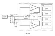
圖2A示意性地示出根據實施例的適於XRF的系統50。如圖所示,系統50包括多個X射線源201和X射線檢測器101。在實施例中,多個X射線源201和X射線檢測器101可以是以芯片的形式安裝在印刷電路板(PCB)上。在實施例中,多個X射線源201和X射線檢測器101可以交替布置。系統50可包括X射線屏蔽,其被配置為防止來自X射線源201的X射線直接到達X射線檢測器101。X射線屏蔽可以包括材料層206,其將X射線源201中的每一個與X射線檢測器101分開。在實施例中,材料層206可以包括,但不限於鎢(W)或鉛(Pb)。在實施例中,材料層206的厚度為1.5-2毫米(mm)。Fig. 2A schematically shows asystem 50 suitable for XRF according to an embodiment. As shown,system 50 includes a plurality ofX-ray sources 201 andX-ray detectors 101 . In an embodiment, the plurality ofX-ray sources 201 and theX-ray detectors 101 may be mounted on a printed circuit board (PCB) in the form of a chip. In an embodiment, a plurality ofX-ray sources 201 andX-ray detectors 101 may be arranged alternately.System 50 may include an X-ray shield configured to prevent X-rays fromX-ray source 201 from directly reachingX-ray detector 101 . The X-ray shield may include a layer ofmaterial 206 that separates each of theX-ray sources 201 from theX-ray detector 101 . In an embodiment, thematerial layer206 may include, but is not limited to, tungsten (W) or lead (Pb). In an embodiment, thematerial layer 206 has a thickness of 1.5-2 millimeters (mm).

來自X射線源201的X射線光子202可以入射在材料樣本298上。當X射線光子202具有比材料樣本298的原子的內部軌道上的電子的電離勢更大的能量時,在所述原子的內部軌道上的電子可以被逐出,在所述內部軌道上留下空位。當原子的外軌道上的電子弛豫以填充內軌道上的空位時,發射熒光X射線光子204(也稱為次級X射線光子)。熒光X射線光子204具有等於外部軌道和內部軌道電子之間的能量差的能量。X-ray photons 202 fromX-ray source 201 may be incident onmaterial sample 298 . When theX-ray photon 202 has an energy greater than the ionization potential of the electrons on the internal orbitals of the atoms of thematerial sample 298, the electrons on the internal orbitals of the atoms may be expelled, leaving vacancy. Fluorescent X-ray photons 204 (also called secondary X-ray photons) are emitted when electrons on the outer orbitals of the atoms relax to fill the vacancies on the inner orbitals.Fluorescent X-ray photons 204 have an energy equal to the energy difference between the outer orbit and inner orbit electrons.

X射線檢測器101可配置成接收熒光X射線光子204,並通過分析接收到的熒光X射線光子204來識別材料樣本298的元素。X-ray detector 101 may be configured to receivefluorescent X-ray photons 204 and to identify elements ofmaterial sample 298 by analyzing the receivedfluorescent X-ray photons 204 .

圖2B示意性地示出根據實施例的系統50的俯視圖。如圖所示,系統50包括多個X射線源201和多個X射線檢測器101,以類似檢查版的交錯方式設置。同樣如圖所示,X射線源201和X射線檢測器101可以由材料層206分開。Fig. 2B schematically shows a top view of asystem 50 according to an embodiment. As shown in the figure, thesystem 50 includes a plurality ofX-ray sources 201 and a plurality ofX-ray detectors 101 arranged in a staggered manner similar to inspection plates. Also as shown, theX-ray source 201 and theX-ray detector 101 may be separated by alayer 206 of material.

圖2C示意性地示出根據實施例的系統50的俯視圖。如圖所示,系統50包括多個X射線源201和多個X射線檢測器101,按這樣的方式安置:每個X射線檢測器101被X射線源201包圍。同樣如圖所示,X射線源201和X射線檢測器101可以由材料層206分隔開。Fig. 2C schematically shows a top view of asystem 50 according to an embodiment. As shown, thesystem 50 includes a plurality ofX-ray sources 201 and a plurality ofX-ray detectors 101 arranged in such a way that eachX-ray detector 101 is surrounded by theX-ray source 201 . Also as shown, theX-ray source 201 and theX-ray detector 101 may be separated by a layer ofmaterial 206 .

圖3A示意性地示出根據實施例的系統50的X射線源201的俯視圖。如圖所示,X射線源201包括多個排列成陣列的X射線產生器299。在該示例中,X射線源201包括多個行的X射線產生器299。在一些例子中,X射線源201可僅包括一行或一列X射線產生器299。Fig. 3A schematically shows a top view of theX-ray source 201 of thesystem 50 according to an embodiment. As shown, theX-ray source 201 includes a plurality ofX-ray generators 299 arranged in an array. In this example, theX-ray source 201 includes a plurality of rows ofX-ray generators 299 . In some examples, theX-ray source 201 may only include one row or one column ofX-ray generators 299 .

圖3B示意性地示出根據實施例的系統50的X射線檢測器101的俯視圖。如圖所示,X射線檢測器101包括排列成陣列的多個圖元199。在該例子中,X射線檢測器101包括多個行的圖元199。在一些例子中,X射線檢測器101可僅包括一行或一列圖元199。Fig. 3B schematically shows a top view of theX-ray detector 101 of thesystem 50 according to an embodiment. As shown, theX-ray detector 101 includes a plurality ofpicture elements 199 arranged in an array. In this example, theX-ray detector 101 includes a plurality of rows ofprimitives 199 . In some examples,X-ray detector 101 may include only one row or column ofprimitives 199 .

圖4示意性地示出:根據實施例,X射線產生器299的截面圖。在這個例子中,X射線產生器299包括第一襯底210,陰極212(例如,多個碳納米管),對電極220,可選的屏蔽電極230,金屬陽極240和可選的第二襯底250。Fig. 4 schematically shows a cross-sectional view of anX-ray generator 299 according to an embodiment. In this example, anX-ray generator 299 includes afirst substrate 210, a cathode 212 (e.g., a plurality of carbon nanotubes), acounter electrode 220, anoptional shield electrode 230, ametal anode 240, and an optional second substrate.Bottom 250.

在實施例中,第一襯底210可以包括但不限於矽或氧化矽。如圖所示,第一襯底210具有凹部215,陰極212形成於第一襯底210的凹部215中。凹部215中陰極212可以包括一個或多個碳納米管。陰極212可配置成在電場下發射電子。電子可以通過表面勢能壘結合在陰極212(例如,碳納米管)中。當向陰極212施加足夠強的電場(例如沿碳納米管的長度方向)時,陰極212中的電子可獲得充足的能量,克服了陰極212的表面勢能壘,進入凹部215中的自由空間。將產生電子到自由空間的這個機制稱為場發射。在實施例中,陰極212電接地。In an embodiment, thefirst substrate 210 may include but not limited to silicon or silicon oxide. As shown, thefirst substrate 210 has aconcave portion 215 , and thecathode 212 is formed in theconcave portion 215 of thefirst substrate 210 . Thecathode 212 in therecess 215 may include one or more carbon nanotubes.Cathode 212 may be configured to emit electrons under an electric field. Electrons can be bound in cathode 212 (eg, carbon nanotubes) through a surface potential barrier. When a sufficiently strong electric field is applied to the cathode 212 (for example, along the length of the carbon nanotube), the electrons in thecathode 212 can obtain sufficient energy, overcome the surface potential energy barrier of thecathode 212, and enter the free space in therecess 215. This mechanism of generating electrons into free space is called field emission. In an embodiment,cathode 212 is electrically grounded.

在實施例中,對電極220位於凹部215的側壁上。對電極220可以相對於陰極212被偏置正電壓+V1,從而提供電場以引起來自陰極212的電子的場發射。如上所述,正電壓+V1建立的電場可為陰極212中的束縛電子提供大於表面勢能壘的能量。同樣如圖4所示,對電極220可由第一襯底210的絕緣體235電絕緣。In an embodiment, thecounter electrode 220 is located on the sidewall of therecess 215 .Counter electrode 220 may be biased with a positive voltage +V1 relative tocathode 212 , thereby providing an electric field to induce field emission of electrons fromcathode 212 . As mentioned above, the electric field established by the positive voltage +V1 can provide the bound electrons in thecathode 212 with energy greater than the surface potential energy barrier. As also shown in FIG. 4 , thecounter electrode 220 may be electrically insulated by theinsulator 235 of thefirst substrate 210 .

圖5A示意性地示出:根據實施例,沿著圖4中的A-A'切線朝向X射線產生器299的橫截面的俯視圖。在這個例子中,在圖4中僅示出:第一襯底210的橫截面,陰極212,對電極220和凹部215。如圖所示,陰極212可以是排列成陣列的碳納米管,並與地面電連接。在該具體例子中,碳納米管排列成矩形陣列。然而,在一些其它例子中,納米管可以排列成任何其它合適形狀的陣列,包括但不限於,圓形陣列、六邊形陣列、以及蜂窩陣列。碳納米管也可以沒有特定的布置。同樣如圖所示,對電極220可以是圍繞第一襯底210的凹部215的側壁的連續環或點環。為了簡明起見,與所述對電極220的電連接未示出。在這個例子中,對電極220沿側壁的整個周邊布置。在一些其它例子中,對電極220可沿側壁的周邊的一部分布置。在圖5A所示的例子中,凹部215具有矩形橫截面並且對電極220也可以是矩形。Fig. 5A schematically shows a top view of a cross-section along the line AA' in Fig. 4 towards theX-ray generator 299, according to an embodiment. In this example, only a cross-section of thefirst substrate 210 , thecathode 212 , thecounter electrode 220 and therecess 215 are shown in FIG. 4 . As shown, thecathode 212 may be carbon nanotubes arranged in an array and electrically connected to ground. In this particular example, the carbon nanotubes are arranged in a rectangular array. However, in some other examples, the nanotubes may be arranged in arrays of any other suitable shape, including, but not limited to, circular arrays, hexagonal arrays, and honeycomb arrays. Carbon nanotubes may also have no specific arrangement. As also shown, thecounter electrode 220 may be a continuous ring or a point ring around the sidewall of therecess 215 of thefirst substrate 210 . For simplicity, the electrical connection to thecounter electrode 220 is not shown. In this example, thecounter electrode 220 runs along the entire perimeter of the sidewalllayout. In some other examples, thecounter electrode 220 may be arranged along a portion of the perimeter of the sidewall. In the example shown in FIG. 5A , therecess 215 has a rectangular cross section and thecounter electrode 220 may also be rectangular.

圖5B示意性地示出:根據另一實施例,沿著圖4中的A-A'切線朝向X射線產生器299的橫截面的俯視圖。不同於圖5A,凹部215的橫截面為圓形,並且對電極220也可以是圓形。Fig. 5B schematically shows a top view of a cross-section of theX-ray generator 299 along the tangent line AA' in Fig. 4 according to another embodiment. Unlike FIG. 5A , the cross section of therecess 215 is circular, and thecounter electrode 220 may also be circular.

返回到圖4,屏蔽電極230可以在凹部215的側壁上並在對電極220與金屬陽極240之間。屏蔽電極230可被適當地偏置以將發射自陽極212的電子排斥離開金屬陽極240,並且因此起X射線產生器299的開關的作用(即,通過X射線產生器299,啟用或禁用X射線光子202的生成)。如圖所示,屏蔽電極230可以通過絕緣體235與對電極220電絕緣。如進一步所示,屏蔽電極230可以不必暴露在凹部215中。在實施例中,屏蔽電極230可以具有與對電極220相似的形狀。Returning to FIG. 4 , theshield electrode 230 may be on the sidewall of therecess 215 and between thecounter electrode 220 and themetal anode 240 .Shield electrode 230 may be suitably biased to repel electrons emitted fromanode 212 away frommetal anode 240, and thus act as a switch for X-ray generator 299 (i.e., enable or disable X-rays throughX-ray generator 299 Generation of photons 202). As shown,shield electrode 230 may be electrically insulated fromcounter electrode 220 byinsulator 235 . As further shown, theshield electrode 230 may not necessarily be exposed in therecess 215 . In an embodiment, theshield electrode 230 may have a shape similar to that of thecounter electrode 220 .

當屏蔽電極230相對於陰極212被提供有足夠負的電壓-V2時,屏蔽電極230可將發射自陰極212的電子排斥離開金屬陽極240。沒有電子撞擊金屬陽極240,X射線光子202的生成被禁用。當屏蔽電極230沒有足夠負偏置時,來自陰極212的電子可以撞擊金屬陽極240,並且X射線光子202的產生被啟用。Whenshield electrode 230 is provided with a sufficiently negative voltage −V2 relative tocathode 212 ,shield electrode 230 may repel electrons emitted fromcathode 212 away frommetal anode 240 . With no electrons striking themetal anode 240, the generation ofX-ray photons 202 is disabled. Whenshield electrode 230 is not sufficiently negatively biased, electrons fromcathode 212 may strikemetal anode 240 and the generation ofX-ray photons 202 is enabled.

圖6A示意性地示出:根據實施例,沿著圖4中的B-B'切線朝向X射線產生器299的橫截面的俯視圖。在這個例子中,圖4中僅示出:第一襯底210的橫截面,陰極212和屏蔽電極230。如圖所示,陰極212可以是排列在陣列中的碳納米管並與地面電連接。在該具體例子中,碳納米管排列成矩形陣列。然而,在一些其它例子中,納米管可以排列成任意其它合適形狀的陣列,包括,但不限於,圓形陣列,六邊形陣列,和蜂窩陣列。碳納米管也可以沒有特定的布置。同樣如圖所示,屏蔽電極230可以是圍繞第一襯底210的凹部215的側壁的連續環或點環。為了簡明起見,與屏蔽電極230的電連接未示出。在該例子中,屏蔽電極230沿側壁的整個周邊布置。在一些其它例子中,屏蔽電極230可以沿著側壁的周邊的一部分布置。在圖6A所示的例子中,凹部215具有矩形橫截面並且屏蔽電極230也可以是矩形。Fig. 6A schematically shows a top view of a cross section along the tangent line BB' in Fig. 4 towards theX-ray generator 299, according to an embodiment. In this example, only: a cross-section of thefirst substrate 210 , thecathode 212 and theshield electrode 230 are shown in FIG. 4 . As shown,cathode 212 may be carbon nanotubes arranged in an array and electrically connected to ground. In this particular example, the carbon nanotubes are arranged in a rectangular array. However, in some other examples, the nanotubes may be arranged in arrays of any other suitable shape, including, but not limited to, circular arrays, hexagonal arrays, and honeycomb arrays. Carbon nanotubes may also have no specific arrangement. As also shown, theshield electrode 230 may be a continuous ring or a point ring around the sidewall of therecess 215 of thefirst substrate 210 . For simplicity, the electrical connection to shieldelectrode 230 is not shown. In this example, theshield electrode 230 is arranged along the entire perimeter of the sidewall. In aIn some other examples, theshield electrode 230 may be disposed along a portion of the perimeter of the sidewall. In the example shown in FIG. 6A , therecess 215 has a rectangular cross section and theshield electrode 230 may also be rectangular.

圖6B示意性地示出:根據另一實施例,沿著圖4中B-B'切線朝向X射線產生器299的橫截面的俯視圖。不同於圖6A,凹部215的橫截面為圓形,並且屏蔽電極230也可以是圓形。Fig. 6B schematically shows a top view of a cross-section of theX-ray generator 299 along the tangent line BB' in Fig. 4 according to another embodiment. Unlike FIG. 6A , the cross section of therecess 215 is circular, and theshield electrode 230 may also be circular.

返回到圖4,在實施例中,第二襯底250可以是玻璃襯底或對感興趣的X射線具有低衰減的襯底。在實施例中,第二襯底250可以包括但不限於矽或氧化矽。第二襯底250可允許X射線光子202通過。如圖所示,金屬陽極240位於第二襯底250的下面(即,在面對陰極212的一側上),其共同位於絕緣體235上。在另一實施例中,金屬陽極240可布置在凹部215上(不具有第二襯底250)。Returning to FIG. 4 , in an embodiment, thesecond substrate 250 may be a glass substrate or a substrate with low attenuation of the X-rays of interest. In an embodiment, thesecond substrate 250 may include but not limited to silicon or silicon oxide.Second substrate 250 may allowX-ray photons 202 to pass through. As shown,metal anode 240 is located underneath second substrate 250 (ie, on the side facing cathode 212 ), which is co-located oninsulator 235 . In another embodiment, themetal anode 240 may be disposed on the recess 215 (without the second substrate 250).

金屬陽極240可以相對於陰極212被偏置正電壓+V3。來自陽極212的電子,如果沒有被屏蔽電極230排斥,則被這個電壓建立的電場向金屬陽極240加速。金屬陽極240可以包括,但不限於,鎢,鉬,錸,銅或它們的組合。當電子在撞擊金屬陽極240之前獲得足夠的動能(例如,大於10kev,50kev,80kev,100kev,130kev等)時,可在高速自由電子撞擊金屬陽極240後產生X射線光子202。Metal anode 240 may be biased with a positive voltage +V3 relative tocathode 212 . Electrons from theanode 212, if not repelled by theshield electrode 230, are directed toward the metal anode by the electric field established by this voltage.Pole 240 acceleration.Metal anode 240 may include, but is not limited to, tungsten, molybdenum, rhenium, copper, or combinations thereof.X-ray photons 202 may be generated after high-speed free electrons strike themetal anode 240 when the electrons gain sufficient kinetic energy (eg, greater than 10 kev, 50 kev, 80 kev, 100 kev, 130 kev, etc.) before striking themetal anode 240 .

圖7示意性地示出根據實施例適合於使用X射線源201的X射線檢測器100。該檢測器具有圖元150的陣列。陣列可以是矩形陣列、蜂窩狀陣列、六邊形陣列或任何其他適合的陣列。每個圖元150配置成檢測其上入射的X射線光子並且測量X射線光子的能量。例如,每個圖元150配置成在一段時間內對其上入射的、能量落在多個倉中的X射線光子的數目計數。所有圖元150可配置成在相同時段內對其上入射的、能量在多個倉內的X射線光子的數目計數。每個圖元150可具有它自己的模數轉換器(ADC),其配置成使代表入射X射線光子的能量的類比信號數字化為數位信號。對於XRF應用,具有10位或更高的解析度的ADC是有用的。每個圖元150可配置成測量它的暗電流,例如在每個X射線光子入射在其上之前或與之並發。每個圖元150可配置成從其上入射的X射線光子的能量減去暗電流的貢獻。圖元150可配置成並行操作。例如,在一個圖元150測量入射X射線光子時,另一個圖元150可等待X射線光子到達。圖元150可不必獨立可尋址。Fig. 7 schematically shows anX-ray detector 100 suitable for use with anX-ray source 201 according to an embodiment. The detector has an array ofprimitives 150 . The array can be a rectangular array, a honeycomb array, a hexagonal array, or any other suitable array. Each primitive 150 is configured to detect x-ray photons incident thereon and measure the energy of the x-ray photons. For example, eachbin 150 is configured to count the number of x-ray photons incident thereon having energies falling in a plurality of bins over a period of time. Allbins 150 may be configured to count the number of X-ray photons incident thereon with energies within multiple bins within the same time period. Eachpicture element 150 may have its own analog-to-digital converter (ADC) configured to digitize an analog signal representing the energy of an incident X-ray photon into a digital signal. For XRF applications, ADCs with a resolution of 10 bits or higher are useful. Each primitive 150 can be configured to measureIts dark current, for example, precedes or is concurrent with each X-ray photon incident on it. Eachbin 150 may be configured to subtract the dark current contribution from the energy of an X-ray photon incident thereon.Primitives 150 may be configured to operate in parallel. For example, while one primitive 150 measures an incident X-ray photon, another primitive 150 may wait for the X-ray photon to arrive.Primitives 150 may not necessarily be independently addressable.

檢測器100可具有至少100、2500、10000個或更多的圖元150。檢測器100可配置成使所有圖元150所計數的具有相同能量範圍的倉的X射線光子的數目相加。例如,檢測器100可使圖元150存儲在能量從70KeV到71KeV的倉中的數目相加、使圖元150存儲在能量從71KeV到72KeV的倉中的數目相加,等等。檢測器100可將倉的相加數字編輯為檢測器100上入射的X射線光子的能譜。Thedetector 100 may have at least 100, 2500, 10000 ormore primitives 150 . Thedetector 100 may be configured to sum the number of x-ray photons counted by allbins 150 for bins having the same energy range. For example,detector 100 may sum the number ofprimitives 150 stored in bins with energy from 70 KeV to 71 KeV, sum the number ofprimitives 150 stored in bins with energy from 71 KeV to 72 KeV, and so on. Thedetector 100 may digitally compile the addition of the bins into the energy spectrum of the X-ray photons incident on thedetector 100 .

圖8示意性地示出根據實施例的檢測器100的框圖。在步驟151,每個圖元150可測量其上入射的X射線光子的能量。X射線光子的能量在步驟152中被數字化(例如,由ADC)到多個倉153A、153B、153C…中的一個。倉153A、153B、153C…每個分別具有對應的計數器154A、154B和154C。當能量分配到倉內時,對應計數器中存儲的數目增加一。檢測器100可使對應於圖元150中的相同能量範圍的倉的所有計數器中存儲的數目相加。例如,所有圖元150中的所有計數器(例如,154A,154B,154C)中存儲的數目可相加並且存儲在相同能量範圍的全局計數器(例如,100A,100B,100C)中。所有全局計數器中存儲的數目可編輯為檢測器100上入射的X射線的能譜。Fig. 8 schematically shows a block diagram of adetector 100 according to an embodiment. Atstep 151, each bin 150 may measure the energy of an X-ray photon incident thereon. The energy of the X-ray photons is digitized (e.g., by an ADC) instep 152 to one of a plurality ofbins 153A, 153B, 153C...indivual. Thebins 153A, 153B, 153C... each have acorresponding counter 154A, 154B and 154C, respectively. When energy is dispensed into a bin, the number stored in the corresponding counter is incremented by one.Detector 100 may sum the numbers stored in all counters corresponding to bins of the same energy range in primitive 150 . For example, the numbers stored in all counters (eg, 154A, 154B, 154C) in allprimitives 150 may be summed and stored in a global counter (eg, 100A, 100B, 100C) of the same energy range. The numbers stored in all global counters can be programmed into the energy spectrum of the X-rays incident on thedetector 100 .

圖9A示意示出根據實施例的檢測器100的橫截面圖。檢測器100可包括X射線吸收層110和電子層120(例如,ASIC),用於處理或分析入射X射線在X射線吸收層110中產生的電信號。在實施例中,檢測器100不包括閃爍體。X射線吸收層110可包括半導體材料,例如矽、鍺、GaAs、CdTe、CdZnTe或其組合。半導體對於感興趣的X射線能量可具有高的質量衰減系數。Fig. 9A schematically shows a cross-sectional view of adetector 100 according to an embodiment. Thedetector 100 may include anX-ray absorbing layer 110 and an electronic layer 120 (for example, an ASIC) for processing or analyzing electrical signals generated in theX-ray absorbing layer 110 by incident X-rays. In an embodiment,detector 100 does not include a scintillator. TheX-ray absorbing layer 110 may include semiconductor materials such as silicon, germanium, GaAs, CdTe, CdZnTe or combinations thereof. Semiconductors can have high mass attenuation coefficients for x-ray energies of interest.

如在圖9B中的檢測器100的詳細橫截面所示,根據實施例,X射線吸收層110可包括由第一摻雜區111、第二摻雜區113的一個或多個離散區114形成的一個或多個二極體(例如,p-i-n或p-n)。第二摻雜區113可通過本征區112(可選)而與第一摻雜區111分離。離散部分114通過第一摻雜區111或本征區112而彼此分離。第一摻雜區111和第二摻雜區113具有相反類型的摻雜(例如,區111是p型並且區113是n型,或區111是n型並且區113是p型)。在圖9B中的示例中,第二摻雜區113的離散區114中的每個與第一摻雜區111和本征區112(可選)一起形成二極體。即,在圖9B中的示例中,X射線吸收層110具有多個二極體,其具有第一摻雜區111作為共用電極。第一摻雜區111還可具有離散部分。As shown in the detailed cross-section of thedetector 100 in FIG. 9B , according to an embodiment, theX-ray absorbing layer 110 may include one or morediscrete regions 114 formed from a firstdoped region 111 , a seconddoped region 113 One or more diodes (eg, p-i-n or p-n) of the The seconddoped region 113 may be separated from the firstdoped region 111 by an (optional)intrinsic region 112 . Thediscrete portions 114 are separated from each other by the firstdoped region 111 or theintrinsic region 112 . The firstdoped region 111 and the seconddoped region 113 have opposite types of doping (eg,region 111 is p-type andregion 113 is n-type, orregion 111 is n-type andregion 113 is p-type). In the example in FIG. 9B , each of thediscrete regions 114 of the seconddoped region 113 forms a diode together with the firstdoped region 111 and (optionally) theintrinsic region 112 . That is, in the example in FIG. 9B , theX-ray absorbing layer 110 has a plurality of diodes having the firstdoped region 111 as a common electrode. The firstdoped region 111 may also have discrete portions.

當X射線光子撞擊X射線吸收層110(其包括二極體)時,X射線光子可被吸收並且通過多個機制產生一個或多個載荷子。一個X射線光子可產生10至100000個載荷子。載荷子可在電場下向二極體中的一個的電極漂移。場可以是外部電場。電觸點119B可包括離散部分,其中的每個與離散區114電接觸。在實施例中,載荷子可在多個方向上漂移使得單個X射線光子產生的載荷子大致未被兩個不同離散區114共用(“大致未被共用”在這裏意指這些載荷子中不到2%、不到0.5%、不到0.1%或不到0.01%流向與余下載荷子不同的離散區114中的一個)。在這些離散區114中的一個的足跡周圍入射的X射線光子產生的載荷子大致未與這些離散區114中的另一個共用。與離散區114關聯的圖元150可以是圍繞離散區114的區域,其中由其中入射的X射線光子產生的載荷子中的大致全部(超過98%、超過99.5%、超過99.9%或超過99.99%)流向離散區114。即,這些載荷子中不到2%、不到1%、不到0.1%或不到0.01%流到圖元外。When an X-ray photon strikes the X-ray absorbing layer 110 (which includes a diode), the X-ray photon may be absorbed and generate one or more charge carriers through a number of mechanisms. One X-ray photon can generate 10 to 100,000 charge carriers. The charge carriers can drift towards the electrode of one of the diodes under the electric field.The field may be an external electric field.Electrical contacts 119B may include discrete portions, each of which is in electrical contact withdiscrete regions 114 . In an embodiment, charge carriers may drift in multiple directions such that charge carriers generated by a single X-ray photon are substantially not shared by two distinct discrete regions 114 ("substantially not shared" here means that less than 2%, less than 0.5%, less than 0.1%, or less than 0.01% flow to one of thediscrete regions 114 different from the remaining charge carriers). Charge carriers generated by incident X-ray photons around the footprint of one of thediscrete regions 114 are substantially not shared with the other of thediscrete regions 114 . A primitive 150 associated withdiscrete region 114 may be an area surroundingdiscrete region 114 in which substantially all (more than 98%, more than 99.5%, more than 99.9%, or more than 99.99%) of the charge carriers generated by X-ray photons incident therein ) flows to thediscrete zone 114. That is, less than 2%, less than 1%, less than 0.1%, or less than 0.01% of these charge carriers flow out of the primitive.

如在圖9C中的檢測器100的可供替代的詳細橫截面所示,根據實施例,X射線吸收層110可包括具有半導體材料(例如矽、鍺、GaAs、CdTe、CdZnTe或其組合)的電阻器,但不包括二極體。半導體對於感興趣的X射線能量可具有高的質量衰減系數。As shown in an alternative detailed cross-section ofdetector 100 in FIG. 9C , according to an embodiment, X-ray absorbinglayer 110 may comprise a semiconductor material (e.g., silicon, germanium, GaAs, CdTe,CdZnTe or combinations thereof), but excluding diodes. Semiconductors can have high mass attenuation coefficients for x-ray energies of interest.

在X射線光子撞擊X射線吸收層110(其包括電阻器但不包括二極體)時,它可被吸收並且通過多個機制產生一個或多個載荷子。一個X射線光子可產生10至100000個載荷子。載荷子可在電場下向電觸點119A和119B漂移。場可以是外部電場。電觸點119B包括離散部分。在實施例中,載荷子可在多個方向上漂移使得單個X射線光子產生的載荷子大致未被電觸點119B的兩個不同離散部分共用(“大致未被共用”在這裏意指這些載荷子中不到2%、不到0.5%、不到0.1%或不到0.01%流向與余下載荷子不同的離散區中的一個)。在電觸點119B的這些離散部分中的一個的足跡周圍入射的X射線光子產生的載荷子大致未與電觸點119B的這些離散部分中的另一個共用。與電觸點119B的離散部分關聯的圖元150可以是圍繞離散部分的區域,其中由其中入射的X射線光子產生的載荷子中的大致全部(超過98%、超過99.5%、超過99.9%或超過99.99%)流向電觸點119B的離散部分。即,這些載荷子中不到2%、不到0.5%、不到0.1%或不到0.01%流到與電觸點119B的一個離散部分關聯的圖元外。When an X-ray photon strikes the X-ray absorbing layer 110 (which includes a resistor but not a diode), it can be absorbed and generate one or more charge carriers through a number of mechanisms. One X-ray photon can generate 10 to 100,000 charge carriers. The charge carriers can drift towards theelectrical contacts 119A and 119B under the electric field. The field may be an external electric field.Electrical contacts 119B include discrete portions. In an embodiment, the charge carriers may drift in multiple directions such that the charge carriers generated by a single X-ray photon are substantially not shared by two different discrete portions of theelectrical contact 119B ("substantially not shared" here means that these loads Less than 2%, less than 0.5%, less than 0.1%, or less than 0.01% of the charge flow to one of the discrete regions different from the remaining charge carriers). Charge carriers generated by incident X-ray photons around the footprint of one of the discrete portions ofelectrical contact 119B are substantially not shared with the other of the discrete portions ofelectrical contact 119B. A primitive 150 associated with a discrete portion ofelectrical contact 119B may be an area surrounding the discrete portion in which substantially all (more than 98%, more than 99.5%, more than 99.9%, or More than 99.99%) flow to the discretepart. That is, less than 2%, less than 0.5%, less than 0.1%, or less than 0.01% of the charge carriers flow out of the primitive associated with a discrete portion of theelectrical contact 119B.

電子層120可包括電子系統121,其適合於處理或解釋X射線吸收層110上入射的X射線光子產生的信號。電子系統121可包括類比電路,例如濾波網路、放大器、整合器和比較器,或數位電路,例如微處理器和記憶體。電子系統121可包括圖元共用的部件或專用於單個圖元的部件。例如,電子系統121可包括專用於每個圖元的放大器和在所有圖元之間共用的微處理器。電子系統121可通過通孔131電連接到圖元。通孔之間的空間可用填充材料130填充,其可使電子層120到X射線吸收層110的連接的機械穩定性增加。在不使用通孔的情況下使電子系統121連接到圖元的其他接合技術是可能的。Theelectronics layer 120 may comprise anelectronics system 121 suitable for processing or interpreting signals generated by X-ray photons incident on theX-ray absorbing layer 110 .Electronic system 121 may include analog circuits, such as filter networks, amplifiers, integrators, and comparators, or digital circuits, such as microprocessors and memories.Electronic system 121 may include components that are common to primitives or components that are specific to individual primitives. For example,electronic system 121 may include an amplifier dedicated to each picture element and a microprocessor shared among all picture elements. Theelectronic system 121 may be electrically connected to the graphics element through thevia 131 . The space between the via holes may be filled with a fillingmaterial 130 which may increase the mechanical stability of the connection of theelectronic layer 120 to theX-ray absorbing layer 110 . Other bonding techniques are possible to connect theelectronics system 121 to the primitive without using vias.

圖10A和圖10B各自示出根據實施例的電子系統121的部件圖。電子系統121可包括第一電壓比較器301,第二電壓比較器302,多個計數器320(包括計數器320A,320B,320C,320D,…),開關305,ADC306,以及控制器310。10A and 10B each show a component diagram of anelectronic system 121 according to an embodiment. Theelectronic system 121 may include afirst voltage comparator 301, asecond voltage comparator 302, a plurality of counters320 (includingcounters 320A, 320B, 320C, 320D, . . . ),switch 305 ,ADC 306 , andcontroller 310 .

第一電壓比較器301配置成將電觸點119B的離散部分的電壓與第一閾值比較。第一電壓比較器301可配置成直接監測電壓,或通過對一段時間內流過二極體或電觸點的電流整合來計算電壓。第一電壓比較器301可由控制器310可控地啟動或停用。第一電壓比較器301可以是連續比較器。即,第一電壓比較器301可配置成被連續啟動,並且連續監測電壓。配置為連續比較器的第一電壓比較器301使電子系統121錯過由入射X射線光子產生的信號的機會減少。配置為連續比較器的第一電壓比較器301在入射X射線強度相對高時尤其適合。第一電壓比較器301可以是鐘控比較器,其具有較低功耗的益處。配置為鐘控比較器的第一電壓比較器301可導致系統121錯過由一些入射X射線光子產生的信號。在入射X射線強度低時,錯過入射輻射X射線光子的機會因為兩個連續光子之間的間隔相對長而低。因此,配置為鐘控比較器的第一電壓比較器301在入射X射線強度相對低時尤其適合。第一閾值可以是一個入射X射線光子可在半導體電觸點119B中產生的最大電壓的1-5%、5-10%、10%-20%、20-30%、30-40%或40-50%。最大電壓可取決於入射X射線光子的能量(即,入射X射線的波長),X射線吸收層110的材料和其它因素。例如,第一閾值可以是50mV、100mV、150mV或200mV。Thefirst voltage comparator 301 is configured to compare the voltage of the discrete portion of theelectrical contact 119B to a first threshold. Thefirst voltage comparator 301 may be configured to monitor the voltage directly, or to calculate the voltage by integrating the current flowing through a diode or electrical contact over a period of time. Thefirst voltage comparator 301 can be controllably enabled or disabled by thecontroller 310 . Thefirst voltage comparator 301 may be a continuous comparator. That is, thefirst voltage comparator 301 may be configured to be continuously enabled, and to continuously monitor the voltage. Thefirst voltage comparator 301 configured as a serial comparator reduces the chance of theelectronic system 121 missing a signal generated by an incident X-ray photon. Thefirst voltage comparator 301 configured as a continuous comparator is especially suitable when the incident X-ray intensity is relatively high. Thefirst voltage comparator 301 may be a clocked comparator, which has the benefit of lower power consumption. Thefirst voltage comparator 301 configured as a clocked comparator may cause thesystem 121 to miss the signal generated by some of the incident X-ray photons. At low incident X-ray intensities, the chance of missing a photon of incident radiation X-rays is low because the interval between two consecutive photons is relatively long. Therefore, withThefirst voltage comparator 301 configured as a clocked comparator is particularly suitable when the incident X-ray intensity is relatively low. The first threshold may be 1-5%, 5-10%, 10%-20%, 20-30%, 30-40%, or 40% of the maximum voltage that an incident X-ray photon can generate in the semiconductor electrical contact 119B. -50%. The maximum voltage may depend on the energy of incident X-ray photons (ie, the wavelength of incident X-rays), the material of theX-ray absorbing layer 110, and other factors. For example, the first threshold may be 50mV, 100mV, 150mV or 200mV.

第二電壓比較器302配置成將電壓與第二閾值比較。第二電壓比較器302可配置成直接監測電壓,或通過對一段時間內流過二極體或電觸點的電流整合來計算電壓。第二電壓比較器302可以是連續比較器。第二電壓比較器302可由控制器310可控地啟動或停用。在停用第二電壓比較器302時,第二電壓比較器302的功耗可以是啟動第二電壓比較器302時的功耗的不到1%、不到5%、不到10%或不到20%。第二閾值的絕對值大於第一閾值的絕對值。如本文使用的,術語實數x的“絕對值”或“模數”|x|是x的非負值而不考慮它的符號。即,

Figure 107119243-A0305-02-0029-1
。第二閾值可以是第一閾值的200%-300%。例如,第二閾值可以是100mV、150mV、200mV、250mV或300mV。第二電壓比較器302和第一電壓比較器301可以是相同部件。即,系統121可具有一個電壓比較器,其可以在不同時間將電壓與兩個不同閾值比較。Thesecond voltage comparator 302 is configured to compare the voltage to a second threshold. Thesecond voltage comparator 302 may be configured to monitor the voltage directly, or to calculate the voltage by integrating the current flowing through a diode or electrical contact over a period of time. Thesecond voltage comparator 302 may be a continuous comparator. Thesecond voltage comparator 302 can be controllably enabled or disabled by thecontroller 310 . When thesecond voltage comparator 302 is deactivated, the power consumption of thesecond voltage comparator 302 may be less than 1%, less than 5%, less than 10%, or none of the power consumption when thesecond voltage comparator 302 is enabled. to 20%. The absolute value of the second threshold is greater than the absolute value of the first threshold. As used herein, the term "absolute value" or "modulus" of a real numberx |x | is the non-negative value ofx without regard to its sign. Right now,
Figure 107119243-A0305-02-0029-1
. The second threshold may be 200%-300% of the first threshold. For example, the second threshold may be 100 mV, 150 mV, 200 mV, 250 mV or 300 mV. Thesecond voltage comparator 302 and thefirst voltage comparator 301 may be the same component. That is,system 121 may have one voltage comparator that can compare the voltage to two different thresholds at different times.

第一電壓比較器301或第二電壓比較器302可包括一個或多個運算放大器或任何其他適合的電路。第一電壓比較器301或第二電壓比較器302可具有高的速度以允許電子系統121在高通量的入射X射線下操作。然而,具有高的速度通常以功耗為代價。Thefirst voltage comparator 301 or thesecond voltage comparator 302 may include one or more operational amplifiers or any other suitable circuit. Thefirst voltage comparator 301 or thesecond voltage comparator 302 may have a high speed to allow theelectronic system 121 to operate at a high flux of incident X-rays. However, having high speed usually comes at the expense of power consumption.

計數器320可以是軟體部件(例如,電腦記憶體中存儲的數字)或硬體部件(例如,4017 IC和7490 IC)。每個計數器320與對於一個能量範圍的倉關聯。例如,計數器320A可與70-71KeV的倉關聯,計數器320B可與71-72KeV的倉關聯,計數器320C可與72-73KeV的倉關聯,計數器320D可與73-74KeV的倉關聯。當入射X射線光子的能量由ADC 306確定為在與計數器320關聯的倉中時,計數器320中記錄的數字增加一。Counter 320 can be a software component (eg, a number stored in computer memory) or a hardware component (eg, 4017 IC and 7490 IC). Eachcounter 320 is associated with a bin for an energy range. For example,counter 320A may be associated with the 70-71 KeV bin,counter 320B may be associated with the 71-72 KeV bin,counter 320C may be associated with the 72-73 KeV bin, and counter 320D may be associated with the 73-74 KeV bin. When the energy of an incident X-ray photon is determined byADC 306 to be in the bin associated withcounter 320, the number recorded incounter 320 is incremented by one.

控制器310可以是例如微控制器和微處理器等硬體部件。控制器310配置成從第一電壓比較器301確定電壓的絕對值等於或超出第一閾值的絕對值(例如,電壓的絕對值從第一閾值的絕對閾值以下增加到等於或超過第一閾值的絕對值的值)的時刻啟動時間延遲。在這裏因為電壓可以是負的或正的而使用絕對值,這取決於是使用二極體的陰極還是陽極或哪個電觸點的電壓。控制器310可配置成在第一電壓比較器301確定電壓的絕對值等於或超出第一閾值的絕對值的時間之前,保持停用第二電壓比較器302、計數器320和第一電壓比較器301的操作不需要的任何其他電路。時間延遲可在電壓變穩定(即,電壓的變化率大致為零)之後終止。短語“電壓的變化率大致為零”意指電壓的時間變化小於0.1%/ns。短語“電壓的變化率大致為非零”意指電壓的時間變化是至少0.1%/ns。Controller 310 may be a hardware component such as a microcontroller and a microprocessor. Thecontroller 310 is configured to determine from thefirst voltage comparator 301 that the absolute value of the voltage equals or exceeds the absolute value of the first threshold (e.g., the absolute value of the voltage increases from below the absolute threshold of the first threshold to equal to or exceeds the first threshold). absolute value) at which the time delay is started. Absolute values are used here because the voltage can be negative or positive, depending on whether the cathode or anode of the diode or which electrical contact's voltage is used. Thecontroller 310 may be configured to keep thesecond voltage comparator 302, thecounter 320, and thefirst voltage comparator 301 disabled until the time when thefirst voltage comparator 301 determines that the absolute value of the voltage equals or exceeds the absolute value of the first threshold operation of any other circuitry not required. The time delay may terminate after the voltage becomes stable (ie, the rate of change of the voltage is approximately zero). The phrase "the rate of change of the voltage is substantially zero" means that the temporal change of the voltage is less than 0.1%/ns. The phrase "the rate of change of the voltage is substantially non-zero" means that the temporal change of the voltage is at least 0.1%/ns.

控制器310可配置成在時間延遲期間(其包括開始和終止)啟動第二電壓比較器。在實施例中,控制器310配置成在時間延遲開始時啟動第二電壓比較器。術語“啟動”意指促使部件進入操作狀態(例如,通過發送諸如電壓脈沖或邏輯電平等信號、通過提供電力等)。術語“停用”意指促使部件進入非操作狀態(例如,通過發送諸如電壓脈沖或邏輯電平等信號、通過切斷電力等)。操作狀態可具有比非操作狀態更高的功耗(例如,高10倍、高100倍、高1000倍)。控制器310本身可被停用直到第一電壓比較器301的輸出在電壓的絕對值等於或超出第一閾值的絕對值時啟動控制器310。Thecontroller 310 may be configured to enable the second voltage comparator during a time delay (which includes start and end). In an embodiment, thecontroller 310 is configured to activate the second voltage comparator at the beginning of the time delay. The term "enable" means causing a component to enter an operational state (eg, by sending a signal such as a voltage pulse or logic level, by providing power, etc.). The term "deactivation" means causing a componentEntering a non-operational state (eg, by sending a signal such as a voltage pulse or logic level, by cutting off power, etc.). The operational state may have higher power consumption (eg, 10 times higher, 100 times higher, 1000 times higher) than the non-operational state. Thecontroller 310 itself may be disabled until the output of thefirst voltage comparator 301 activates thecontroller 310 when the absolute value of the voltage equals or exceeds the absolute value of the first threshold.

如果在時間延遲期間第二電壓比較器302確定電壓的絕對值等於或超出第二閾值的絕對值,並且X射線光子能量落入與計數器320相關聯的倉,控制器310可配置成促使計數器320記錄的數目增加一。If during the time delay thesecond voltage comparator 302 determines that the absolute value of the voltage equals or exceeds the absolute value of the second threshold, and the X-ray photon energy falls into the bin associated with thecounter 320, thecontroller 310 may be configured to cause thecounter 320 The number of records is incremented by one.

控制器310可配置成在時間延遲終止時使ADC 306將電壓數字化並且基於所述電壓確定X射線光子的能量落在哪個倉中。Controller 310 may be configured to causeADC 306 to digitize the voltage at the expiration of the time delay and determine, based on the voltage, into which bin the energy of the X-ray photon falls.

控制器310可配置成使電觸點119B連接到電接地,以便使電壓重定並且使電觸點119B上累積的任何載荷子放電。在實施例中,電觸點119B在時間延遲終止後連接到電接地。在實施例中,電觸點119B在有限復位時期連接到電接地。控制器310可通過控制開關305而使電觸點119B連接到電接地。開關可以是電晶體,例如場效應電晶體(FET)。Controller 310 may be configured to connectelectrical contact 119B to electrical ground in order to reset the voltage and discharge any charge carriers accumulated onelectrical contact 119B. In an embodiment,electrical contact 119B is connected to electrical ground after the time delay expires. In an embodiment, theelectrical contact 119B has a limited reset periodConnect to electrical ground.Controller 310 may connectelectrical contact 119B to electrical ground by controllingswitch 305 . The switches may be transistors, such as field effect transistors (FETs).

在實施例中,系統121沒有類比濾波器網路(例如,RC網路)。在實施例中,系統121沒有類比電路。In an embodiment,system 121 has no analog filter network (eg, RC network). In an embodiment,system 121 has no analog circuitry.

ADC306可將它測量的電壓作為類比或數位信號饋送給控制器310。ADC可以是逐次逼近型寄存器(SAR)ADC(也叫作逐次逼近ADC)。SAR ADC在最終匯聚於類比信號的數位輸出之前經由通過所有可能量化等級的二進位搜索來使類比信號數字化。SAR ADC可具有四個主要子電路:采樣和保持電路(用於獲取輸入電壓(Vin)),內部數模轉換器(DAC)(其配置成對類比電壓比較器供應等於逐次逼近型寄存器(SAR)的數位代碼輸出的類比電壓),類比電壓比較器(其將Vin與內部DAC的輸出比較並且向SAR輸出比較結果),SAR(其被配置成向內部DAC供應Vin的逼近數位代碼)。SAR可被初始化使得最高有效位(MSB)等於數位1。該代碼被饋送到內部DAC內,其然後將該數位代碼的類比等效物(Vref/2)供應到比較器用於與Vin比較。如果該類比電壓超出Vin,比較器促使SAR將該位重定;否則,該位留1。然後SAR的下一個位設置為1並且進行相同測試,從而繼續該二進位搜索直到SAR中的每個位被測試。所得的代碼是Vin的數位逼近並且最後在數字化結束時由SAR輸出。ADC 306 may feed the voltage it measures tocontroller 310 as an analog or digital signal. The ADC may be a successive approximation register (SAR) ADC (also known as a successive approximation ADC). The SAR ADC digitizes the analog signal via a binary search through all possible quantization levels before finally converging on the digital output of the analog signal. A SAR ADC can have four main subcircuits: a sample and hold circuit (used to obtain the input voltage (Vin)), an internal digital-to-analog converter (DAC) configured to supply an analog voltage comparator equal to the successive approximation register (SAR ), the analog voltage comparator (which compares Vin with the output of the internal DAC and outputs the comparison result to the SAR), the SAR (which is configured to supply the approximate digital code of Vin to the internal DAC). The SAR may be initialized such that the most significant bit (MSB) is equal to bit one. the generationThe code is fed into an internal DAC, which then supplies the analog equivalent of the digital code (Vref/2) to a comparator for comparison with Vin. If the analog voltage exceeds Vin, the comparator causes the SAR to reset this bit; otherwise, this bit remains 1. Then the next bit of the SAR is set to 1 and the same is tested, continuing this binary search until every bit in the SAR is tested. The resulting code is a digital approximation of Vin and is finally output by the SAR at the end of digitization.

電子系統121可包括電容器模組309,其電連接到電觸點119B,其中電容器模組配置成從電觸點119B收集載荷子。電容器模組能包括放大器的回饋路徑中的電容器。如此配置的放大器叫作電容跨阻放大器(CTIA)。CTIA通過防止放大器飽和而具有高的動態範圍並且通過限制信號路徑中的帶寬來提高信噪比。來自電極的載荷子在一段時間(“整合期”)(例如,如在圖11中示出的,在ts至t0之間)內在電容器上累積。在整合期終止後,電容器電壓由ADC306采樣並且然後由重定開關將其重定。電容器模組309能包括直接連接到電觸點119B的電容器。Theelectronic system 121 may include acapacitor module 309 electrically connected to theelectrical contact 119B, wherein the capacitor module is configured to collect charge carriers from theelectrical contact 119B. Capacitor modules can include capacitors in the feedback path of the amplifier. An amplifier so configured is called a capacitive transimpedance amplifier (CTIA). CTIA has high dynamic range by preventing amplifier saturation and improves signal-to-noise ratio by limiting bandwidth in the signal path. Charge carriers from the electrodes accumulate on the capacitor over a period of time (the "integration period") (eg, between ts and t0 as shown in FIG. 11 ). After the integration period expires, the capacitor voltage is sampled byADC 306 and then reset by the reset switch.Capacitor module 309 can include capacitors connected directly toelectrical contacts 119B.

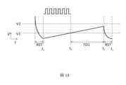
圖11示意示出由與電觸點119B相關聯的圖元150上入射的X射線光子產生的載荷子引起的流過電觸點119B的電流的時間變化(上曲線)和電觸點119B的電壓的對應時間變化(下曲線)。電壓可以是電流關於時間的整合。在時間t0,X射線光子撞擊二極體或電阻器,載荷子開始在圖元150中產生,電流開始流過電觸點119B,並且電觸點119B電壓的絕對值開始增加。在時間t1,第一電壓比較器301確定電壓的絕對值等於或超出第一閾值V1的絕對值,控制器310啟動時間延遲TD1並且控制器310可在TD1開始時停用第一電壓比較器301。如果控制器310在t1之前被停用,在t1啟動控制器310。在TD1期間,控制器310啟動第二電壓比較器302。如這裏使用的術語在時間延遲“期間”意指開始和終止(即,結束)和中間的任何時間。例如,控制器310可在TD1終止時啟動第二電壓比較器302。如果在TD1期間,第二電壓比較器302確定在時間t2電壓的絕對值等於或超出第二閾值的絕對值,控制器310等待電壓的穩定化變穩定。電壓在時間te穩定,這時X射線光子產生的所有載荷子漂移出X射線吸收層110。在時間ts,時間延遲TD1終止。在時間te或時間te之後,控制器310使ADC306數字化電壓,並確定X射線光子的能量落入哪個倉。控制器310引起所述倉對應的計數器320記錄的數字增加一。在圖11的例子中,時間ts在時間te之後;即TD1在X射線光子產生的所有載荷子漂移出第一輻射吸收層110之後終止。如果時間不能容易地測量,TD1可以經驗地選取,以允許足夠的時間收集由X射線光子產生的幾乎所有載荷子,但又不太長以至於沒有另一個入射X射線光子的風險。即,TD 1能被經驗地選取,以至於時間ts經驗地在時間te之後。時間ts不必再時間te之後,因為控制器310可以拋棄TD1,一旦達到V2,並且等待時間te。電壓和暗電流引起的電壓貢獻的差異的變化率從而在ts大致為零。控制器310可配置成在TD1終止時或在t2或在其中間的任何時間停用第二電壓比較器302。11 schematically shows the time variation (upper curve) of the current flowing through theelectrical contact 119B caused by the charge carriers generated by the incident X-ray photons on thepicture element 150 associated with theelectrical contact 119B (upper curve) and theelectrical contact 119B. The corresponding time variation of the voltage (lower curve). Voltage can be the integration of current with respect to time. At time t0 , the X-ray photons strike the diode or resistor, charge carriers begin to be generated incell 150 , current begins to flow throughelectrical contact 119B, and the absolute value of the voltage atelectrical contact 119B begins to increase. At timet1 , thefirst voltage comparator 301 determines that the absolute value of the voltage equals or exceeds the absolute value of the first threshold V1, thecontroller 310 initiates a time delay TD1 and thecontroller 310 may deactivate the first voltage comparator at the beginning ofTD1 301. If thecontroller 310 was deactivated beforet1 , thecontroller 310 is activated att1 . During TD1, thecontroller 310 enables thesecond voltage comparator 302 . As used herein, the term "during" a time delay means both the beginning and the end (ie, end) and any time in between. For example, thecontroller 310 can enable thesecond voltage comparator 302 when TD1 expires. If during TD1 thesecond voltage comparator 302 determines that the absolute value of the voltage equals or exceeds the absolute value of the second threshold at timet2 , thecontroller 310 waits for the stabilization of the voltage to become stable. The voltagestabilizes at time te when all charge carriers generated by the X-ray photons drift out of theX-ray absorbing layer 110 . At time ts , time delay TD1 terminates. At orafter time te,controller 310causes ADC 306 to digitize the voltage and determine into which bin the energy of the X-ray photon falls. Thecontroller 310 causes the number recorded by thecounter 320 corresponding to the bin to increase by one. In the example of FIG. 11 , time ts is after time te ; ie TD1 ends after all charge carriers generated by X-ray photons have drifted out of the firstradiation absorbing layer 110 . If the time cannot be easily measured, TD1 can be chosen empirically to allow enough time to collect nearly all the charge carriers generated by the X-ray photon, but not so long that there is no risk of another incident X-ray photon. That is,TD 1 can be chosen empirically such that time ts empirically follows time te . Time ts does not have to be after time te becausecontroller 310 can discard TD1 once V2 is reached and wait for time te . The rate of change of the difference in voltage and dark current-induced voltage contributions is thus approximately zero att .Controller 310 may be configured to disablesecond voltage comparator 302 upon termination of TD1 or att2 or any time therebetween.

在時間te電壓與X射線光子產生的載荷子的總量成比例,其與X射線光子的能量有關。控制器310可配置成基於ADC 306的輸出確定X射線光子的能量所落入的倉。The voltage at time te is proportional to the total amount of charge carriers generated by the X-ray photons, which is related to the energy of the X-ray photons. Thecontroller 310 may be configured to determine the bin into which the energy of the X-ray photon falls based on the output of theADC 306 .

在TD1終止或被ADC 306數字化後(取其中朝後者),控制器310在復位期RST使電觸點119B連接到電接地以允許電觸點119B上累積的載荷子流到地面並且使電壓重定。在RST之後,系統121準備檢測另一個入射X射線光子。系統121在圖11的示例中可以應對的入射X射線光子的速率隱式地受限於1/(TD1+RST)。如果第一電壓比較器301被停用,控制器310可以在RST終止之前的任何時間啟動它。如果控制器310被停用,可在RST終止之前啟動它。After TD1 is terminated or digitized by ADC 306 (whichever is the latter),controller 310 connectselectrical contact 119B to electrical ground during reset period RST to allow accumulated charge carriers onelectrical contact 119B to flow to ground and reset the voltage . After the RST, thesystem 121 is ready to detect another incident X-ray photon. The rate of incident X-ray photons thatsystem 121 can handle in the example of FIG. 11 is implicitly limited by 1/(TD1+RST). If thefirst voltage comparator 301 is disabled, thecontroller 310 can enable it at any time before RST is terminated. If thecontroller 310 is disabled, it can be enabled before the RST terminates.

因為檢測器100具有可並行操作的許多圖元150,檢測器可以應對較高速率的入射X射線光子。這是因為特定圖元150上的入射率是整個陣列圖元上的入射率的1/N,其中N是圖元數目。Because thedetector 100 hasmany picture elements 150 that can operate in parallel, the detector can handle a higher rate of incident X-ray photons. This is because the incidence on a particular primitive 150 is 1/N of the incidence on the entire array of primitives, where N is the number of primitives.

圖12示出根據實施例對於圖8中的步驟151的示例流程圖。在步驟701中,例如使用第一電壓比較器301將暴露於X射線光子的二極體的電觸點119B或電阻器的電壓與第一閾值比較。在步驟702中,例如用控制器310確定電壓的絕對值是否等於或超出第一閾值V1的絕對值。如果電壓的絕對值不等於或不超出第一閾值的絕對值,方法回到步驟701。即,在步驟701和步驟702中監測電壓,直到電壓達到V1。如果電壓的絕對值等於或超出第一閾值的絕對值,流程繼續到步驟703。在步驟703中,測量T=(t1-t0)。如關於圖11所解釋的,在時間t0 X射線光子撞擊二極體或電阻器,載荷子開始在圖元150中產生,電流開始流經電觸點119B,電觸點119B的電壓的絕對值開始增加;在時間t1,電壓的絕對值等於或超過第一閾值V1的絕對值。在步驟704中,例如使用控制器310啟動時間延遲TD1。在步驟705中,例如使用第二電壓比較器302將電壓與第二閾值V2比較。在步驟706中,例如使用控制器310確定在TD1期間電壓的絕對值是否等於或超出第二閾值V2的絕對值。如果在TD1期間電壓的絕對值不等於或不超出第二閾值的絕對值,電壓被認為是由暗電流引起的,並且流程回到步驟707。在步驟707中,基於T測量暗電流對電壓的貢獻。在示例中,確定T是否大於先前測量的最大T(Tmax)。如果先前未測量T,Tmax=0。如果T大於Tmax,用T代替Tmax。暗電流對電壓的貢獻處於V1/Tmax的比率。如果測量暗電流(如在該示例中),暗電流的貢獻在時間Tm是((tm-tr)‧V1/Tmax),其中tr是最後復位期的結束。類似本公開中的任何時間間隔,可以通過對脈沖計數(例如,對時鐘周期或時鐘脈沖計數)來測量(tm-tr)。在檢測器100的每個測量之前,Tmax可重定為零。可通過對t1與t0之間的脈沖的數目計數來測量T,如在圖11和圖13中示意示出的。使用T測量暗電流對電壓的貢獻的另一個方式包括提取T分布的參數(例如,T的預期值(Texpected))並且將暗電流對電壓的貢獻率估計為V1/Texpected。在步驟708中,例如通過使電觸點119B連接到電接地,將電壓重定為電接地。如果在TD1期間電壓的絕對值等於或超出第二閾值的絕對值V2,流程繼續到步驟709。在步驟709中,在電壓在時間tm穩定後測量電壓,並且扣除暗電流對測量電壓的貢獻。時間tm可以是TD1終止之後且在RST之前的任何時間。在圖8中在步驟152中將結果提供給ADC。復位期結束的時間(例如,電觸點119B從電接地斷開的時間)是trFIG. 12 shows an example flowchart forstep 151 in FIG. 8 according to an embodiment. Instep 701 , the voltage of theelectrical contact 119B of the diode or the resistor exposed to the X-ray photons is compared with a first threshold, for example using thefirst voltage comparator 301 . Instep 702, it is determined, eg by thecontroller 310, whether the absolute value of the voltage is equal to or exceeds the absolute value of the first threshold V1. If the absolute value of the voltage is not equal to or exceeds the absolute value of the first threshold, the method returns to step 701 . That is, the voltage is monitored insteps 701 and 702 until the voltage reaches V1. If the absolute value of the voltage is equal to or exceeds the absolute value of the first threshold, the flow continues to step 703 . Instep 703, T=(t1 -t0 ) is measured. As explained with respect to FIG. 11 , at time t0 the X-ray photon hits the diode or resistor, charge carriers start to be generated in thepicture element 150, current starts to flow through theelectrical contact 119B, and the absolute value of the voltage of theelectrical contact 119B The value starts to increase; at time t1 , the absolute value of the voltage equals or exceeds the absolute value of the first threshold V1. Instep 704 , time delay TD1 is initiated, forexample using controller 310 . Instep 705, the voltage is compared with a second threshold V2, for example using thesecond voltage comparator 302. Instep 706, it is determined, for example using thecontroller 310, whether the absolute value of the voltage is equal to or exceeds the absolute value of the second threshold V2 during TD1. If the absolute value of the voltage is not equal to or exceeds the absolute value of the second threshold during TD1 , the voltage is considered to be caused by dark current, and the process returns to step 707 . Instep 707, the dark current contribution to the voltage is measured based on T. In an example, it is determined whether T is greater than a previously measured maximum T (Tmax). If T was not previously measured, Tmax=0. If T is greater than Tmax, replace Tmax with T. The dark current contribution to the voltage is in the ratio V1/Tmax. If dark current is measured (as in this example), the dark current contribution at timeTm is ((tm -tr )‧V1/Tmax), wheretr is the end of the last reset period. Like any time interval in this disclosure, (tm - tr ) may be measured by counting pulses (eg, counting clock cycles or clock pulses). Tmax may be reset to zero before each measurement bydetector 100 . T can be measured by counting the number of pulses between t1 and t0 , as schematically shown in FIGS. 11 and 13 . Another way of using T to measure the contribution of dark current to voltage includes extracting parameters of the T distribution (eg, the expected value of T (Texpected)) and estimating the contribution of dark current to voltage as V1/Texpected. Instep 708, the voltage is reset to electrical ground, for example by connectingelectrical contact 119B to electrical ground. If the absolute value of the voltage is equal to or exceeds the absolute value V2 of the second threshold during TD1 , the process continues to step 709 . Instep 709, the voltage is measured after the voltage stabilizes at timetm , and the dark current contribution to the measured voltage is subtracted. Timetm can be any time after TD1 terminates and before RST. The result is provided to the ADC instep 152 in FIG. 8 . The time at which the reset period ends (eg, the time at whichelectrical contact 119B is disconnected from electrical ground) is tr .

圖13示意示出根據實施例由暗電流引起的電觸點119B的電壓的時間變化。在RST後,電壓由於暗電流而增加。暗電流越高,電壓達到V1所花的時間越少(即T越短)。因此,T是暗電流的度量。暗電流不可能大到足以在TD1期間促使電壓達到V2但入射X射線光子引起的電流可能大到足以這麽做。該差異可用於識別暗電流的效應。圖13中的流程可在圖元150測量一系列入射光子時在每個圖元150中實施,這將允許捕捉暗電流的變化(例如,由變化的環境(例如溫度)引起)。FIG. 13 schematically shows the time variation of the voltage of theelectrical contact 119B caused by dark current according to an embodiment. After RST, the voltage increases due to dark current. The higher the dark current, the less time it takes for the voltage to reach V1 (ie, the shorter T). Therefore, T is a measure of dark current. The dark current may not be large enough to drive the voltage to V2 during TD1 but the current induced by the incident X-ray photon may be large enough to do so. This difference can be used to identify the effect of dark current. The flow in FIG. 13 can be implemented in each bin 150 as thebin 150 measures a series of incident photons, which will allow changes in dark current (eg, caused by changing environment (eg, temperature)) to be captured.

半導體X射線檢測器100可用於相襯X射線成像(PCI)(也稱為相敏X射線成像)。PCI包括至少部分地使用由那個物體引起的X射線光束的相移(包括相移的空間分布)形成物體的圖像的技術。一個獲得相移的方法是將相位變換為強度的變化。Thesemiconductor x-ray detector 100 may be used for phase contrast x-ray imaging (PCI) (also known as phase sensitive x-ray imaging). PCI consists of using, at least in part, phaseA technique for forming an image of an object by shifting (including the spatial distribution of phase shifts). One way to obtain a phase shift is to convert the phase into a change in intensity.

PCI能與斷層攝影技術相結合來獲得物體折射率的實數部分的三維分布。PCI比傳統的基於強度的X射線成像(例如,輻射照相術)對物體中的密度變化更敏感。PCI對軟組織進行成像特別有用。PCI can be combined with tomographic techniques to obtain the three-dimensional distribution of the real part of the refractive index of an object. PCI is more sensitive to density changes in objects than conventional intensity-based X-ray imaging (eg, radiography). PCI is particularly useful for imaging soft tissues.

根據實施例,圖14示意性地示出適於PCI的系統1900。系統1900可包括至少兩個X射線檢測器1910和1920。兩個X射線檢測器1910中的一個或兩個都是本文所述的半導體X射線檢測器100。X射線檢測器1910和1920可以由間隔件1930隔開。間隔件1930對X射線可以具有非常小的吸收。例如,間隔件1930可以具有非常小的質量衰減系數(例如,<10cm2g-1,<1cm2g-1,<0.1cm2g-1,或<0.01cm2g-1)。間隔件1930的質量衰減系數可以是均勻的(例如,間隔件1930中每兩個點之間的變化小於5%,小於1%或小於0.1%)。間隔件1930可對穿過間隔件1930的X射線的相位產生相同的變化量。例如,間隔件1930可以是氣體(例如,空氣),真空室,可包括鋁、鈹、矽或其組合。Figure 14 schematically illustrates a PCI-adaptedsystem 1900, according to an embodiment.System 1900 may include at least twoX-ray detectors 1910 and 1920 . One or both of the twoX-ray detectors 1910 aresemiconductor X-ray detectors 100 as described herein.X-ray detectors 1910 and 1920 may be separated by aspacer 1930 . Thespacer 1930 may have very little absorption of X-rays. For example, spacer 1930 may have a very small mass attenuation coefficient (eg, <10 cm2 g−1 , <1 cm2 g−1 , <0.1 cm2 g−1 , or <0.01 cm2 g−1 ). The mass attenuation coefficient of thespacer 1930 may be uniform (eg, less than 5%, less than 1%, or less than 0.1% variation between every two points in the spacer 1930). Thespacer 1930 may produce the same amount of change in the phase of the X-rays passing through thespacer 1930 . For example, spacer 1930 can be a gas (eg, air), a vacuum chamber, and can include aluminum, beryllium, silicon, or combinations thereof.

系統1900可用於獲得被成像物體1960引起的入射X射線1950的相移。入射X射線1950可由一個或多個這裏描述的X射線源201產生。X射線檢測器1910和1920可以同時捕獲兩幅圖像(即,強度分布)。由於X射線檢測器1910和1920由間隔件1930隔開,所述兩幅圖像與所述物體1960的距離不同。相位可以從所述兩幅圖像中確定,例如,使用基於菲涅耳衍射整合的線性化的算法。System 1900 may be used to obtain a phase shift ofincident X-rays 1950 caused by imagedobject 1960 .Incident X-rays 1950 may be generated by one ormore X-ray sources 201 described herein.X-ray detectors 1910 and 1920 can capture two images (ie, intensity distributions) simultaneously. Since theX-ray detectors 1910 and 1920 are separated by thespacer 1930, the distances of the two images from theobject 1960 are different. The phase can be determined from the two images, for example, using an algorithm based on linearization of Fresnel diffraction integration.

根據實施例,圖15示意性地示出適於PCI的系統1800。系統1800包括在此描述的半導體X射線檢測器100。半導體X射線檢測器100被配置為移動到距暴露於入射X射線1850的物體1860的不同距離處並捕獲其圖像。入射X射線1850可由一個或多個這裏描述的X射線源201產生。圖像可不必同時被捕獲。相位可以從圖像確定,例如使用基於菲涅耳衍射整合的線性化的算法。Figure 15 schematically illustrates a PCI-adapted system 1800, according to an embodiment. System 1800 includessemiconductor X-ray detector 100 as described herein.Semiconductor X-ray detector 100 is configured to move to different distances from and capture images of anobject 1860 exposed toincident X-rays 1850 .Incident X-rays 1850 may be generated by one or more of theX-ray sources 201 described herein. The images do not have to be captured at the same time. The phase can be determined from the image, for example using an algorithm based on linearization of Fresnel diffraction integration.

圖16示意性地示出了包括本文所述的輻射檢測器100的系統。該系統可用於醫學成像,例如胸部X射線照相,腹部X射線照相等。系統包括X射線源1201,其可包括一個或多個X射線源201。從X射線源1201發射的X射線穿透物體1202(例如,人體部位如胸部,肢體,腹部),被物體1202的內部結構(例如,骨骼,肌肉,脂肪,器官等)不同程度衰減,並且被投射到半導體X射線檢測器100。半導體X射線檢測器100通過檢測X射線的強度分布而形成圖像。Fig. 16 schematically illustrates a system including aradiation detector 100 as described herein. The system can be used in medical imaging such as chest radiography, abdominal radiography, etc. The system includes anX-ray source 1201 , which may include one ormore X-ray sources 201 . The X-rays emitted from theX-ray source 1201 penetrate the object 1202 (for example, human body parts such as chest, limbs, abdomen), are attenuated to varying degrees by the internal structure of the object 1202 (for example, bones, muscles, fat, organs, etc.), and are Projected to thesemiconductor X-ray detector 100. Thesemiconductor X-ray detector 100 forms an image by detecting the intensity distribution of X-rays.

圖17示意性地示出包括本文所述的半導體X射線檢測器100的系統。該系統可用於醫療成像,例如牙科X射線照相。該系統包括X射線源1301,其可包括一個或多個這裏描述的X射線源201。從X射線源1301發射的X射線穿透物體1302,其是哺乳動物(例如,人)的嘴巴的部分。物體1302可包括上頜骨,腭骨,牙齒,下頜或舌。X射線被物體1302的不同結構不同程度衰減,並被投射到半導體X射線檢測器100。半導體X射線檢測器100通過檢測X射線的強度分布形成圖像。牙齒比齲牙,感染,牙周韌帶更多地吸收X射線。牙科患者接收的X射線輻射的劑量典型地是小的(對全嘴系列約0.150mSv)。Fig. 17 schematically shows a system comprising asemiconductor X-ray detector 100 as described herein. The system can be used in medical imaging such as dental radiography. The system includes anX-ray source 1301, which may include one or more of theX-ray sources 201 described herein. X-rays emitted from anX-ray source 1301 penetrate anobject 1302, which is part of the mouth of a mammal (eg, a human).Object 1302 may include a maxilla, palate, teeth, jaw or tongue. The X-rays are attenuated to different degrees by different structures of theobject 1302 and are projected to thesemiconductor X-ray detector 100 .Semiconductor X-ray detector100 forms an image by detecting the intensity distribution of X-rays. Teeth absorb X-rays more than caries, infections, periodontal ligaments. The dose of X-ray radiation received by dental patients is typically small (about 0.150 mSv for a whole mouth series).

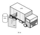
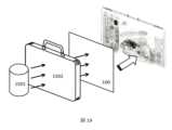
圖18示意性地示出包括本文所述的半導體X射線檢測器100的貨物掃描或非侵入性檢查(NII)系統。該系統可用於檢查和識別例如集裝箱,車輛,船舶,行李等運輸系統中的貨物。該系統包括X射線源1401,其可包括一個或多個X射線源201。從X射線源1401發射的輻射可以從物體1402(例如,集裝箱,車輛,船舶等)背散射並被投射到半導體X射線檢測器100。物體1402的不同內部結構可以不同地背散射X射線。半導體X射線檢測器100通過檢測背散射X射線的強度分布和/或背散射X射線光子的能量來形成圖像。Fig. 18 schematically illustrates a cargo scanning or non-intrusive inspection (NII) system comprising asemiconductor X-ray detector 100 as described herein. The system can be used to inspect and identify goods in transportation systems such as containers, vehicles, ships, luggage, etc. The system includes anX-ray source 1401 , which may include one ormore X-ray sources 201 . Radiation emitted fromX-ray source 1401 may be backscattered from object 1402 (eg, container, vehicle, ship, etc.) and projected tosemiconductor X-ray detector 100 . Different internal structures ofobject 1402 may backscatter X-rays differently. Thesemiconductor X-ray detector 100 forms an image by detecting the intensity distribution of backscattered X-rays and/or the energy of backscattered X-ray photons.

圖19示意性地示出包括本文所述的半導體X射線檢測器100的另一貨物掃描或非侵入性檢查(NII)系統。該系統可用於公共運輸站和機場的行李篩選。該系統包括X射線源1501,其可包括一個或多個X射線源201。從X射線源1501發射的X射線可穿透行李1502,被行李的內容不同地衰減,並被投射到半導體X射線檢測器100。所述半導體X射線檢測器100通過檢測透射X射線的強度分布而形成圖像。該系統可以揭示行李的內容,並識別在公共交通上禁止的物品,例如槍支,毒品,鋒利武器,易燃物。Fig. 19 schematically illustrates another cargo scanning or non-intrusive inspection (NII) system comprising asemiconductor X-ray detector 100 as described herein. The system can be used for luggage at public transport stations and airportsfilter. The system includes anX-ray source 1501 , which may include one ormore X-ray sources 201 . The X-rays emitted from theX-ray source 1501 can penetrate theluggage 1502 , are differently attenuated by the contents of the luggage, and are projected to thesemiconductor X-ray detector 100 . Thesemiconductor X-ray detector 100 forms an image by detecting the intensity distribution of transmitted X-rays. The system can reveal the contents of luggage and identify items prohibited on public transport such as guns, drugs, sharp weapons, flammable objects.

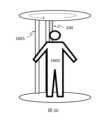
圖20示意性地示出包括本文所述的半導體X射線檢測器100的全身掃描系統。全身掃描系統可以為了安全篩選目的檢測人身體上的物體,不需要物理地移去衣物或進行物理接觸。全身掃描系統能檢測非金屬物體。全身掃描系統包括X射線源1601,其可包括一個或多個X射線源201。從X射線源1601發射的X射線可從被篩選的人1602和其身上的物體背散射,並被投射到半導體X射線檢測器100。所述物體和所述人體可以不同地背散射X射線。半導體X射線檢測器100通過檢測背散射X射線的強度分布來形成圖像。輻射檢測器100和X射線源1601可被配置為沿直線或旋轉方向掃描人。Fig. 20 schematically shows a whole body scanning system including thesemiconductor X-ray detector 100 described herein. A full-body scanning system can detect objects on a person's body for security screening purposes without physically removing clothing or making physical contact. The full body scanning system can detect non-metallic objects. The full body scanning system includes anX-ray source 1601 which may include one ormore X-ray sources 201 . X-rays emitted from theX-ray source 1601 may be backscattered from the screenedperson 1602 and objects on the person, and projected to thesemiconductor X-ray detector 100 . The object and the human body may backscatter x-rays differently. Thesemiconductor X-ray detector 100 forms an image by detecting the intensity distribution of backscattered X-rays.Radiation detector 100 andX-ray source 1601 may be configured to scan a person in a linear or rotational direction.

圖21示意性地示出包括本文所述的半導體X射線檢測器的X射線計算機斷層掃描(X射線CT)系統。X射線CT系統使用計算機處理的X射線來產生被掃描對象的特定區域的斷層圖像(虛擬“切片”)。斷層圖像可用於各種醫學學科中的診斷和治療目的,或用於探傷,故障分析,計量,組裝分析和反向工程。X射線CT系統包括在此描述的半導體X射線檢測器100,以及X射線源1701,其可包括一個或多個X射線源201。半導體X射線檢測器100和X射線源1701可被配置成沿一個或多個圓形或螺旋路徑同步旋轉。Fig. 21 schematically illustrates an X-ray computed tomography (X-ray CT) system including a semiconductor X-ray detector as described herein. X-ray CT systems use computer-processed x-rays to produce tomographic images (virtual "slices") of specific regions of the scanned object. Tomographic images can be used for diagnostic and therapeutic purposes in various medical disciplines, or for flaw detection, failure analysis, metrology, assembly analysis and reverse engineering. An X-ray CT system includes asemiconductor X-ray detector 100 as described herein, and anX-ray source 1701 , which may include one ormore X-ray sources 201 .Semiconductor X-ray detector 100 andX-ray source 1701 may be configured to rotate synchronously along one or more circular or helical paths.

圖22示意性地示出包括本文描述的半導體X射線檢測器100的電子顯微鏡。電子顯微鏡包括被配置為發射電子的電子源1801(也稱為電子槍)。在實施例中,電子源1801可包括一個或多個X射線源201。電子源1801可具有各種發射機制,例如熱離子,光電陰極,冷發射或等離子體源。被發射的電子通過電子光學系統1803,其可被配置為影響、加速或聚焦電子。然後電子到達樣品1802,並且圖像檢測器可從那裏形成圖像。電子顯微鏡可以包括本文所述的輻射檢測器100,用於進行能量色散X射線分光鏡檢查(EDS)。EDS是用於樣品的元素分析或化學表征的分析技術。當電子入射到樣品上時,可從樣品發射特征X射線。入射電子可以激發樣品中的原子的內殼中的電子,從所述殼中將其排出,同時在所述電子原先的位置形成電子空穴。來自外部的高能殼層的電子填充所述空穴,較高能量殼層與較低能量殼層之間的能量差可以按X射線的形式釋放。通過半導體X射線檢測器100可以測量從樣品發射的X射線的數量和能量。Fig. 22 schematically shows an electron microscope comprising asemiconductor X-ray detector 100 as described herein. The electron microscope includes an electron source 1801 (also called an electron gun) configured to emit electrons. In an embodiment,electron source 1801 may include one ormore X-ray sources 201 . Theelectron source 1801 can have various emission mechanisms such as thermionic, photocathode, cold emission or plasma sources. The emitted electrons pass throughelectron optics 1803, which may be configured to influence, accelerate or focus the electrons. The electrons then travel to thesample 1802, and an image detector can form an image from there. electron microscopeTheradiation detector 100 described herein may be included for performing energy dispersive X-ray spectroscopy (EDS). EDS is an analytical technique used for elemental analysis or chemical characterization of samples. When electrons are incident on a sample, characteristic X-rays can be emitted from the sample. Incident electrons can excite electrons in the inner shells of atoms in the sample, expel them from the shells, and form electron holes in their former places. Electrons from the outer high energy shell fill the holes and the energy difference between the higher and lower energy shells can be released in the form of X-rays. The amount and energy of X-rays emitted from a sample can be measured by thesemiconductor X-ray detector 100 .

圖23示意性地示出包括本文所述的半導體X射線檢測器100的輻射劑量儀。輻射劑量儀能夠測量輻射的平均劑量率(例如,來自輻射源1901的X射線)。在實施例中,輻射源可包括一個或多個X射線源201。輻射源1901可包括火山1910或原子彈爆炸。輻射劑量儀可包括室1902,其包括空氣或其它氣體。經過氣體的X射線將使其電離,產生正離子和自由電子。入射光子將產生與其能量成比例的多個這樣的離子對。與輻射劑量儀相關聯的X射線檢測器可以測量在氣體容量上的平均劑量率或交互作用的光子數量。Fig. 23 schematically shows a radiation dosimeter comprising thesemiconductor X-ray detector 100 described herein. Dosimeters are capable of measuring the average dose rate of radiation (eg, X-rays from radiation source 1901). In an embodiment, the radiation source may include one ormore X-ray sources 201 . Theradiation source 1901 may include avolcano 1910 or an atomic bomb explosion. A radiation dosimeter may include achamber 1902 that includes air or other gas. X-rays passing through the gas will ionize it, producing positive ions and free electrons. An incident photon will generate a number of such ion pairs proportional to its energy. X-ray detectors associated with dosimeters can measure the average dose rate or number of interacting photons across the gas volume.

圖24示意性地示出包括本文所述的半導體X射線檢測器100的元素分析儀。元素分析儀能夠檢測在諸如玩具的物體上的一個或多個感興趣的元素的存在。高能量的帶電粒子束(諸如電子或質子,或X射線束)被引導到物體上。在實施例中,高能束,例如,X射線束可由X射線產生器299產生。物體的原子被激發並在特定波長處發射X射線(其是元素的特征)。X射線檢測器100接收所述被發射的X射線並基於所述被發射的X射線的能量確定所述元素的存在。例如,X射線檢測器100可被配置為檢測位於鉛發射的波段的X射線。如果X射線檢測器100從物體上確實接受到在這些波段的X射線,就能知道鉛存在。本文描述的半導體X射線檢測器100可具有其它應用,比如在X射線望遠鏡,X射線乳房攝影,工業X射線缺陷檢測,X射線顯微或微成像,X射線鑄造檢查,X射線無損檢測,X射線焊接檢查,X射線數位減影血管攝影等中。使用該半導體X射線檢測器100適合於代替攝影板,攝影膠片,PSP板,X射線圖像增強器,閃爍體或另一個半導體X射線檢測器。Fig. 24 schematically shows an elemental analyzer comprising thesemiconductor X-ray detector 100 described herein. Elemental analyzers are capable of detecting the presence of one or more elements of interest on an object such as a toy. High-energy beams of charged particles, such as electrons or protons, or X-ray beams, are directed at the object. In an embodiment, a high energy beam, eg, an X-ray beam may be generated by theX-ray generator 299 . The atoms of the object are excited and emit X-rays at specific wavelengths (which are characteristic of the elements). TheX-ray detector 100 receives the emitted X-rays and determines the presence of the elements based on the energy of the emitted X-rays. For example, theX-ray detector 100 may be configured to detect X-rays in the wavelength band emitted by lead. If theX-ray detector 100 actually receives X-rays in these wavelength bands from the object, it can know that lead exists. Thesemiconductor X-ray detector 100 described herein may have other applications, such as in X-ray telescopes, X-ray mammography, industrial X-ray defect detection, X-ray microscopy or microimaging, X-ray casting inspection, X-ray non-destructive testing, X-ray X-ray welding inspection, X-ray digital subtraction angiography, etc. Use of thesemiconductor X-ray detector 100 is suitable for use in place of a photographic plate, photographic film, PSP panel, X-ray image intensifier, scintillator or another semiconductor X-ray detector.

盡管本文公開各種方面和實施例,其它方面和實施例對於本領域內技術人員將變得明顯。本文公開的各種方面和實施例是為了說明目的而不意在為限制性的,其真正範圍和精神由下列權利要求指示。Although various aspects and embodiments are disclosed herein, other aspects and embodiments will become apparent to those skilled in the art. The various aspects and embodiments disclosed herein are for purposes of illustration and are not intended to be limiting, with the true scope and spirit being indicated by the following claims.

50:系統50: system

101:X射線檢測器101:X-ray detector

201:X射線源201: X-ray source

202:X射線光子202: X-ray photons

204:熒光X射線光子204: Fluorescent X-ray photons

206:材料層206: material layer

298:材料樣本298: Material samples

Claims (26)

Translated fromChinese
一種X射線源,其包括:在第一襯底的凹部中的陰極;在所述凹部的側壁上的對電極,其被配置為引起來自所述陰極的電子的場發射;金屬陽極,其被配置為接收從陰極發射的電子,並且通過所述金屬陽極上電子撞擊發射X射線;以及所述對電極和所述金屬陽極之間的屏蔽電極,所述屏蔽電極被配置為防止所有所述電子到達所述金屬陽極。An X-ray source comprising: a cathode in a recess of a first substrate; a counter electrode on a sidewall of the recess configured to cause field emission of electrons from the cathode; a metal anode held by configured to receive electrons emitted from the cathode, and to emit x-rays by electron impingement on the metal anode; and a shield electrode between the counter electrode and the metal anode, the shield electrode configured to prevent all of the electrons to the metal anode.如申請專利範圍第1項之X射線源,其中,所述陰極包括多個碳納米管。According to the X-ray source of claim 1, wherein the cathode includes a plurality of carbon nanotubes.如申請專利範圍第1項之X射線源,其中,所述對電極是圍繞所述側壁的連續環或點環。The X-ray source according to claim 1 of the patent application, wherein the counter electrode is a continuous ring or a point ring surrounding the side wall.如申請專利範圍第1項之X射線源,其中,所述屏蔽電極為圍繞所述側壁的連續環或點環。The X-ray source according to item 1 of the scope of the patent application, wherein the shielding electrode is a continuous ring or a point ring surrounding the side wall.如申請專利範圍第1項之X射線源,其中,所述第一襯底包括矽或氧化矽。The X-ray source of claim 1, wherein the first substrate includes silicon or silicon oxide.如申請專利範圍第1項之X射線源,其中,所述金屬陽極包括從由鎢、鉬、錸、銅及其組合組成的組群中選取的一種或多種金屬。As for the X-ray source of item 1 of the patent application, wherein the metal anode includes one or more metals selected from the group consisting of tungsten, molybdenum, rhenium, copper and combinations thereof.如申請專利範圍第1項之X射線源,還包括結合到所述第一襯底的第二襯底,其中所述第二襯底覆蓋所述凹部。The X-ray source according to Claim 1 of the patent application, further comprising a second substrate bonded to the first substrate, wherein the second substrate covers the concave portion.如申請專利範圍第7項之X射線源,其中所述金屬陽極由所述第二襯底支持。The X-ray source of claim 7, wherein the metal anode is supported by the second substrate.如申請專利範圍第8項之X射線源,其中所述金屬陽極位於所述第二襯底朝向所述陰極的一側。The X-ray source according to claim 8 of the patent application, wherein the metal anode is located on the side of the second substrate facing the cathode.如申請專利範圍第1項之X射線源,其中所述陰極包括碳納米管陣列。As the X-ray source of claim 1, wherein the cathode includes a carbon nanotube array.如申請專利範圍第1項之X射線源,其中所述屏蔽電極被配置為藉由將所述電子排斥離開所述金屬陽極以防止所有所述電子到達所述金屬陽極。The X-ray source of claim 1, wherein the shielding electrode is configured to prevent all of the electrons from reaching the metal anode by repelling the electrons away from the metal anode.如申請專利範圍第1項之X射線源,其中所述屏蔽電極與所述對電極電絕緣。The X-ray source of claim 1, wherein the shielding electrode is electrically insulated from the counter electrode.如申請專利範圍第1項之X射線源,其中所述屏蔽電極未暴露在所述凹部中。The X-ray source of claim 1, wherein the shielding electrode is not exposed in the recess.一種包括X射線源和X射線檢測器的系統,其包含:申請專利範圍第1項的多個X射線源,多個X射線檢測器,其中X射線源和X射線檢測器交替排列;X射線屏蔽,其被配置為防止來自X射線源的X射線直接到達X射線檢測器。A system including an X-ray source and an X-ray detector, which includes: multiple X-ray sources and multiple X-ray detectors according to item 1 of the scope of patent application, wherein the X-ray sources and X-ray detectors are arranged alternately; the X-ray A shield configured to prevent X-rays from the X-ray source from directly reaching the X-ray detector.如申請專利範圍第14項之系統,其中所述X射線屏蔽是X射線檢測器與X射線源之間的材料層。The system of claim 14, wherein the X-ray shield is a layer of material between the X-ray detector and the X-ray source.如申請專利範圍第15項之系統,其中所述材料層包括鎢(W)或鉛(Pb)。The system of claim 15, wherein the material layer includes tungsten (W) or lead (Pb).如申請專利範圍第16項之系統,其中所述材料層的厚度為1.5-2mm。As the system of item 16 of the patent application, wherein the thickness of the material layer is 1.5-2mm.一種包括X射線源和X射線檢測器的系統,其包括如申請專利範圍第1項之X射線源和X射線檢測器,其中所述系統被配置用於對人體胸部或腹部進行X射線照相。A system including an X-ray source and an X-ray detector, which includes the X-ray source and the X-ray detector according to claim 1 of the scope of the patent application, wherein the system is configured for X-ray photography of human chest or abdomen.一種包括X射線源和X射線檢測器的系統,其包括如申請專利範圍第1項之X射線源和X射線檢測器,其中所述系統配置用於對人的嘴巴進行X射線照相。A system including an X-ray source and an X-ray detector, which includes the X-ray source and the X-ray detector according to claim 1 of the patent scope, wherein the system is configured for X-ray photography of a person's mouth.一種貨物掃描或非侵入性檢查(NII)系統,其包括如申請專利範圍第1項的X射線源和X射線檢測器,其中所述貨物掃描或非侵入性檢查系統被配置成基於背散射X射線形成圖像。A cargo scanning or non-invasive inspection (NII) system comprising an X-ray source and an X-ray detector according to claim 1, wherein the cargo scanning or non-invasive inspection system is configured to be based on backscattered X-ray The rays form an image.一種貨物掃描或非侵入性檢查(NII)系統,其包括如申請專利範圍第1項的X射線源和X射線檢測器,其中,所述貨物掃描或非侵入性檢查(NII)系統被配置成基於穿過被檢查的物體的X射線形成圖像。A cargo scanning or non-invasive inspection (NII) system, which includes an X-ray source and an X-ray detector as claimed in claim 1 of the scope of the patent application, wherein the cargo scanning or non-invasive inspection (NII) system is configured as An image is formed based on X-rays passing through the object being inspected.一種全身掃描系統,其包括如申請專利範圍第1項的X射線源和X射線檢測器。A whole-body scanning system, which includes an X-ray source and an X-ray detector as described in item 1 of the scope of the patent application.一種X射線計算機斷層掃描(CT)系統,其包括如申請專利範圍第1項的X射線源和X射線檢測器。An X-ray computed tomography (CT) system, which includes an X-ray source and an X-ray detector as described in item 1 of the scope of the patent application.一種適用於相襯X射線成像(PCI)的系統,所述系統包括申請專利範圍第1項的X射線源和X射線檢測器。A system suitable for phase-contrast X-ray imaging (PCI), the system includes the X-ray source and X-ray detector of the first item in the scope of the patent application.一種元素分析儀,其包括如申請專利範圍第1項的X射線源。An element analyzer, which includes the X-ray source as claimed in item 1 of the scope of the patent application.一種適於檢測X射線熒光(XRF)的系統,所述系統包括申請專利範圍第1項的X射線源和X射線檢測器。A system suitable for detecting X-ray fluorescence (XRF), said system comprising the X-ray source and X-ray detector of claim 1 of the scope of the patent application.
TW107119243A2017-07-262018-06-05An integrated x-ray source, system and element analyzer comprising x-ray sourceTWI788362B (en)

Applications Claiming Priority (3)

Application NumberPriority DateFiling DateTitle
PCT/CN2017/094442WO2019019042A1 (en)2017-07-262017-07-26An integrated x-ray source
??PCT/CN2017/0944422017-07-26
WOPCT/CN2017/0944422017-07-26

Publications (2)

Publication NumberPublication Date
TW201911973A TW201911973A (en)2019-03-16
TWI788362Btrue TWI788362B (en)2023-01-01

Family

ID=65041014

Family Applications (1)

Application NumberTitlePriority DateFiling Date
TW107119243ATWI788362B (en)2017-07-262018-06-05An integrated x-ray source, system and element analyzer comprising x-ray source

Country Status (5)

CountryLink
US (1)US11289300B2 (en)
EP (1)EP3658030A4 (en)
CN (1)CN111093502B (en)
TW (1)TWI788362B (en)
WO (1)WO2019019042A1 (en)

Citations (6)

* Cited by examiner, † Cited by third party
Publication numberPriority datePublication dateAssigneeTitle
US5144191A (en)*1991-06-121992-09-01McncHorizontal microelectronic field emission devices
TW200630149A (en)*2004-11-032006-09-01Nano Proprietary IncPhotocatalytic process
US20090052615A1 (en)*2006-02-022009-02-26Koninklijke Philips Electronics N.V.Imaging apparatus using distributed x-ray souces and method thereof
CN102420088A (en)*2011-12-052012-04-18李驰Back grid type grid-controllable cold cathode X-ray tube
US20130230147A1 (en)*2012-03-052013-09-05Futaba CorporationX-Ray Tube
CN104470173A (en)*2013-09-182015-03-25清华大学 X-ray device and CT equipment with the X-ray device

Family Cites Families (35)

* Cited by examiner, † Cited by third party
Publication numberPriority datePublication dateAssigneeTitle
US3882339A (en)*1974-06-171975-05-06Gen ElectricGridded X-ray tube gun
US4982096A (en)*1988-01-061991-01-01Hitachi Medical CorporationMulti-element radiation detector
US5975975A (en)*1994-09-161999-11-02Micron Technology, Inc.Apparatus and method for stabilization of threshold voltage in field emission displays
FI97647C (en)*1994-11-141997-01-27Ima Engineering Ltd Oy Method and apparatus for determining the content of an element
US5872422A (en)*1995-12-201999-02-16Advanced Technology Materials, Inc.Carbon fiber-based field emission devices
JP4079503B2 (en)*1998-04-272008-04-23日本電子株式会社 Analytical electron microscope
JP2001153961A (en)*1999-11-302001-06-08Shimadzu Corp Two-dimensional array type radiation detector
US20040240616A1 (en)2003-05-302004-12-02Applied Nanotechnologies, Inc.Devices and methods for producing multiple X-ray beams from multiple locations
DE10211081A1 (en)*2002-03-132003-10-16Siemens AgX-ray observation and monitoring system for patient in hospital has movable table with conventional X-ray machine at one end and computer tomography at one end
US6934354B2 (en)*2003-05-022005-08-23General Electric CompanyCollimator assembly having multi-piece components
US7412026B2 (en)*2004-07-022008-08-12The Board Of Regents Of The University Of OklahomaPhase-contrast x-ray imaging systems and methods
US20070189459A1 (en)*2006-02-162007-08-16Stellar Micro Devices, Inc.Compact radiation source
JP2007311186A (en)*2006-05-182007-11-29Hamamatsu Photonics KkX-ray tube
US20080187093A1 (en)*2007-02-062008-08-07John Scott PriceX-ray generation using secondary emission electron source
CN101101848B (en)*2007-08-102011-04-27东南大学 Field Emission Cathode X-Ray Tube
US7433443B1 (en)*2007-08-292008-10-07General Electric CompanySystem and method of CT imaging with second tube/detector patching
JP2009087633A (en)*2007-09-282009-04-23Toshiba Corp X-ray source and method of manufacturing x-ray source
EP2212902A4 (en)*2007-11-012016-12-07Rapiscan Systems IncMultiple screen detection systems
WO2010061332A1 (en)*2008-11-262010-06-03Philips Intellectual Property & Standards GmbhAuxiliary grid electrode for x-ray tubes
US8530845B2 (en)*2009-02-042013-09-10Trustees Of Boston UniversitySynthesis of advanced scintillators via vapor deposition techniques
US8588372B2 (en)*2009-12-162013-11-19General Electric CompanyApparatus for modifying electron beam aspect ratio for X-ray generation
US8401151B2 (en)*2009-12-162013-03-19General Electric CompanyX-ray tube for microsecond X-ray intensity switching
JP5769244B2 (en)*2010-07-302015-08-26株式会社リガク Industrial X-ray tube
US9599577B2 (en)*2010-09-062017-03-21Koninklijke Philips N.V.X-ray imaging with pixelated detector
JP2012110579A (en)*2010-11-262012-06-14Fujifilm CorpRadiation tube device and radiation imaging system
EP2649634B1 (en)*2010-12-102018-07-04Canon Kabushiki KaishaRadiation generating apparatus and radiation imaging apparatus
US8897419B1 (en)*2011-02-142014-11-25Science Research Laboratory, Inc.Systems and methods for accelerating charged particle beams
US9470799B2 (en)*2011-05-132016-10-18Unfors Raysafe AbRadiation meter and method
JP5672147B2 (en)*2011-05-242015-02-18コニカミノルタ株式会社 Chest diagnosis support information generation system
US9058954B2 (en)*2012-02-202015-06-16Georgia Tech Research CorporationCarbon nanotube field emission devices and methods of making same
CN103901057B (en)*2012-12-312019-04-30同方威视技术股份有限公司 Item inspection device using distributed X-ray sources
CN203059724U (en)*2013-01-022013-07-17上海联影医疗科技有限公司Scatter resistant grid, integrated component of detector and collimator and X-ray device
CN104411081A (en)*2014-11-132015-03-11重庆大学Linear array micro-nano focus X-ray source for micro-nano CT (computer tomography) system
EP3281040B1 (en)*2015-04-072021-11-24Shenzhen Xpectvision Technology Co., Ltd.Semiconductor x-ray detector
WO2016203954A1 (en)*2015-06-182016-12-22株式会社日立製作所Radiation detector and x-ray ct apparatus provided therewith

Patent Citations (6)

* Cited by examiner, † Cited by third party
Publication numberPriority datePublication dateAssigneeTitle
US5144191A (en)*1991-06-121992-09-01McncHorizontal microelectronic field emission devices
TW200630149A (en)*2004-11-032006-09-01Nano Proprietary IncPhotocatalytic process
US20090052615A1 (en)*2006-02-022009-02-26Koninklijke Philips Electronics N.V.Imaging apparatus using distributed x-ray souces and method thereof
CN102420088A (en)*2011-12-052012-04-18李驰Back grid type grid-controllable cold cathode X-ray tube
US20130230147A1 (en)*2012-03-052013-09-05Futaba CorporationX-Ray Tube
CN104470173A (en)*2013-09-182015-03-25清华大学 X-ray device and CT equipment with the X-ray device

Also Published As

Publication numberPublication date
TW201911973A (en)2019-03-16
WO2019019042A1 (en)2019-01-31
US20200161075A1 (en)2020-05-21
CN111093502A (en)2020-05-01
CN111093502B (en)2023-09-22
EP3658030A1 (en)2020-06-03
EP3658030A4 (en)2021-06-30
US11289300B2 (en)2022-03-29

Similar Documents

PublicationPublication DateTitle
US10955570B2 (en)X-ray detectors capable of managing charge sharing
TWI756337B (en)A radiation detector
US10948613B2 (en)X-ray detectors capable of identifying and managing charge sharing
TWI788320B (en)Radiation detectors, systems for detecting radiation, devices using radiation detectors, and methods for allocating memory
CN112601981A (en)Radiation detector
US20210026025A1 (en)X-ray detector capable of managing charge sharing at its periphery
TW201910809A (en) Radiation detector and method of outputting data therefrom
US11714204B2 (en)Detector for X-ray fluorescence
TWI788362B (en)An integrated x-ray source, system and element analyzer comprising x-ray source
TW202006398A (en)A radiation detector

[8]ページ先頭

©2009-2025 Movatter.jp