TWI787498B - A memory device comprising an electrically floating body transistor - Google Patents
A memory device comprising an electrically floating body transistorDownload PDFInfo
- Publication number
- TWI787498B TWI787498BTW108113471ATW108113471ATWI787498BTW I787498 BTWI787498 BTW I787498BTW 108113471 ATW108113471 ATW 108113471ATW 108113471 ATW108113471 ATW 108113471ATW I787498 BTWI787498 BTW I787498B
- Authority
- TW
- Taiwan
- Prior art keywords
- region
- floating body
- memory
- body region
- memory cell
- Prior art date
Links
Images


Classifications
- G—PHYSICS
- G11—INFORMATION STORAGE
- G11C—STATIC STORES
- G11C13/00—Digital stores characterised by the use of storage elements not covered by groups G11C11/00, G11C23/00, or G11C25/00
- G11C13/0002—Digital stores characterised by the use of storage elements not covered by groups G11C11/00, G11C23/00, or G11C25/00 using resistive RAM [RRAM] elements
- H—ELECTRICITY
- H10—SEMICONDUCTOR DEVICES; ELECTRIC SOLID-STATE DEVICES NOT OTHERWISE PROVIDED FOR
- H10B—ELECTRONIC MEMORY DEVICES
- H10B12/00—Dynamic random access memory [DRAM] devices
- H10B12/20—DRAM devices comprising floating-body transistors, e.g. floating-body cells
- G—PHYSICS
- G11—INFORMATION STORAGE
- G11C—STATIC STORES
- G11C11/00—Digital stores characterised by the use of particular electric or magnetic storage elements; Storage elements therefor
- G11C11/02—Digital stores characterised by the use of particular electric or magnetic storage elements; Storage elements therefor using magnetic elements
- G11C11/16—Digital stores characterised by the use of particular electric or magnetic storage elements; Storage elements therefor using magnetic elements using elements in which the storage effect is based on magnetic spin effect
- G11C11/165—Auxiliary circuits
- G11C11/1659—Cell access
- G—PHYSICS
- G11—INFORMATION STORAGE
- G11C—STATIC STORES
- G11C11/00—Digital stores characterised by the use of particular electric or magnetic storage elements; Storage elements therefor
- G11C11/21—Digital stores characterised by the use of particular electric or magnetic storage elements; Storage elements therefor using electric elements
- G11C11/22—Digital stores characterised by the use of particular electric or magnetic storage elements; Storage elements therefor using electric elements using ferroelectric elements
- G11C11/225—Auxiliary circuits
- G11C11/2259—Cell access
- G—PHYSICS
- G11—INFORMATION STORAGE
- G11C—STATIC STORES
- G11C11/00—Digital stores characterised by the use of particular electric or magnetic storage elements; Storage elements therefor
- G11C11/21—Digital stores characterised by the use of particular electric or magnetic storage elements; Storage elements therefor using electric elements
- G11C11/34—Digital stores characterised by the use of particular electric or magnetic storage elements; Storage elements therefor using electric elements using semiconductor devices
- G11C11/40—Digital stores characterised by the use of particular electric or magnetic storage elements; Storage elements therefor using electric elements using semiconductor devices using transistors
- G11C11/401—Digital stores characterised by the use of particular electric or magnetic storage elements; Storage elements therefor using electric elements using semiconductor devices using transistors forming cells needing refreshing or charge regeneration, i.e. dynamic cells
- G11C11/402—Digital stores characterised by the use of particular electric or magnetic storage elements; Storage elements therefor using electric elements using semiconductor devices using transistors forming cells needing refreshing or charge regeneration, i.e. dynamic cells with charge regeneration individual to each memory cell, i.e. internal refresh
- G11C11/4023—Digital stores characterised by the use of particular electric or magnetic storage elements; Storage elements therefor using electric elements using semiconductor devices using transistors forming cells needing refreshing or charge regeneration, i.e. dynamic cells with charge regeneration individual to each memory cell, i.e. internal refresh using field effect transistors
- G—PHYSICS
- G11—INFORMATION STORAGE
- G11C—STATIC STORES
- G11C11/00—Digital stores characterised by the use of particular electric or magnetic storage elements; Storage elements therefor
- G11C11/21—Digital stores characterised by the use of particular electric or magnetic storage elements; Storage elements therefor using electric elements
- G11C11/34—Digital stores characterised by the use of particular electric or magnetic storage elements; Storage elements therefor using electric elements using semiconductor devices
- G11C11/40—Digital stores characterised by the use of particular electric or magnetic storage elements; Storage elements therefor using electric elements using semiconductor devices using transistors
- G11C11/401—Digital stores characterised by the use of particular electric or magnetic storage elements; Storage elements therefor using electric elements using semiconductor devices using transistors forming cells needing refreshing or charge regeneration, i.e. dynamic cells
- G11C11/403—Digital stores characterised by the use of particular electric or magnetic storage elements; Storage elements therefor using electric elements using semiconductor devices using transistors forming cells needing refreshing or charge regeneration, i.e. dynamic cells with charge regeneration common to a multiplicity of memory cells, i.e. external refresh
- G11C11/404—Digital stores characterised by the use of particular electric or magnetic storage elements; Storage elements therefor using electric elements using semiconductor devices using transistors forming cells needing refreshing or charge regeneration, i.e. dynamic cells with charge regeneration common to a multiplicity of memory cells, i.e. external refresh with one charge-transfer gate, e.g. MOS transistor, per cell
- G—PHYSICS
- G11—INFORMATION STORAGE
- G11C—STATIC STORES
- G11C13/00—Digital stores characterised by the use of storage elements not covered by groups G11C11/00, G11C23/00, or G11C25/00
- G11C13/0002—Digital stores characterised by the use of storage elements not covered by groups G11C11/00, G11C23/00, or G11C25/00 using resistive RAM [RRAM] elements
- G11C13/0021—Auxiliary circuits
- G11C13/003—Cell access
- G—PHYSICS
- G11—INFORMATION STORAGE
- G11C—STATIC STORES
- G11C14/00—Digital stores characterised by arrangements of cells having volatile and non-volatile storage properties for back-up when the power is down
- G11C14/0009—Digital stores characterised by arrangements of cells having volatile and non-volatile storage properties for back-up when the power is down in which the volatile element is a DRAM cell
- G11C14/0027—Digital stores characterised by arrangements of cells having volatile and non-volatile storage properties for back-up when the power is down in which the volatile element is a DRAM cell and the nonvolatile element is a ferroelectric element
- G—PHYSICS
- G11—INFORMATION STORAGE
- G11C—STATIC STORES
- G11C14/00—Digital stores characterised by arrangements of cells having volatile and non-volatile storage properties for back-up when the power is down
- G11C14/0009—Digital stores characterised by arrangements of cells having volatile and non-volatile storage properties for back-up when the power is down in which the volatile element is a DRAM cell
- G11C14/0036—Digital stores characterised by arrangements of cells having volatile and non-volatile storage properties for back-up when the power is down in which the volatile element is a DRAM cell and the nonvolatile element is a magnetic RAM [MRAM] element or ferromagnetic cell
- G—PHYSICS
- G11—INFORMATION STORAGE
- G11C—STATIC STORES
- G11C14/00—Digital stores characterised by arrangements of cells having volatile and non-volatile storage properties for back-up when the power is down
- G11C14/0009—Digital stores characterised by arrangements of cells having volatile and non-volatile storage properties for back-up when the power is down in which the volatile element is a DRAM cell
- G11C14/0045—Digital stores characterised by arrangements of cells having volatile and non-volatile storage properties for back-up when the power is down in which the volatile element is a DRAM cell and the nonvolatile element is a resistive RAM element, i.e. programmable resistors, e.g. formed of phase change or chalcogenide material
- H—ELECTRICITY
- H10—SEMICONDUCTOR DEVICES; ELECTRIC SOLID-STATE DEVICES NOT OTHERWISE PROVIDED FOR
- H10B—ELECTRONIC MEMORY DEVICES
- H10B63/00—Resistance change memory devices, e.g. resistive RAM [ReRAM] devices
- H10B63/30—Resistance change memory devices, e.g. resistive RAM [ReRAM] devices comprising selection components having three or more electrodes, e.g. transistors
- H—ELECTRICITY
- H10—SEMICONDUCTOR DEVICES; ELECTRIC SOLID-STATE DEVICES NOT OTHERWISE PROVIDED FOR
- H10D—INORGANIC ELECTRIC SEMICONDUCTOR DEVICES
- H10D30/00—Field-effect transistors [FET]
- H10D30/60—Insulated-gate field-effect transistors [IGFET]
- H10D30/711—Insulated-gate field-effect transistors [IGFET] having floating bodies
- H—ELECTRICITY
- H10—SEMICONDUCTOR DEVICES; ELECTRIC SOLID-STATE DEVICES NOT OTHERWISE PROVIDED FOR
- H10N—ELECTRIC SOLID-STATE DEVICES NOT OTHERWISE PROVIDED FOR
- H10N70/00—Solid-state devices having no potential barriers, and specially adapted for rectifying, amplifying, oscillating or switching
- H10N70/20—Multistable switching devices, e.g. memristors
- H—ELECTRICITY
- H10—SEMICONDUCTOR DEVICES; ELECTRIC SOLID-STATE DEVICES NOT OTHERWISE PROVIDED FOR
- H10N—ELECTRIC SOLID-STATE DEVICES NOT OTHERWISE PROVIDED FOR
- H10N70/00—Solid-state devices having no potential barriers, and specially adapted for rectifying, amplifying, oscillating or switching
- H10N70/801—Constructional details of multistable switching devices
- H10N70/881—Switching materials
- H10N70/883—Oxides or nitrides
- G—PHYSICS
- G11—INFORMATION STORAGE
- G11C—STATIC STORES
- G11C2211/00—Indexing scheme relating to digital stores characterized by the use of particular electric or magnetic storage elements; Storage elements therefor
- G11C2211/401—Indexing scheme relating to cells needing refreshing or charge regeneration, i.e. dynamic cells
- G11C2211/4016—Memory devices with silicon-on-insulator cells
- G—PHYSICS
- G11—INFORMATION STORAGE
- G11C—STATIC STORES
- G11C2213/00—Indexing scheme relating to G11C13/00 for features not covered by this group
- G11C2213/70—Resistive array aspects
- G11C2213/79—Array wherein the access device being a transistor
- H—ELECTRICITY
- H10—SEMICONDUCTOR DEVICES; ELECTRIC SOLID-STATE DEVICES NOT OTHERWISE PROVIDED FOR
- H10B—ELECTRONIC MEMORY DEVICES
- H10B61/00—Magnetic memory devices, e.g. magnetoresistive RAM [MRAM] devices
- H10B61/20—Magnetic memory devices, e.g. magnetoresistive RAM [MRAM] devices comprising components having three or more electrodes, e.g. transistors
- H—ELECTRICITY
- H10—SEMICONDUCTOR DEVICES; ELECTRIC SOLID-STATE DEVICES NOT OTHERWISE PROVIDED FOR
- H10D—INORGANIC ELECTRIC SEMICONDUCTOR DEVICES
- H10D30/00—Field-effect transistors [FET]
- H10D30/60—Insulated-gate field-effect transistors [IGFET]
- H10D30/62—Fin field-effect transistors [FinFET]
Landscapes
- Engineering & Computer Science (AREA)
- Computer Hardware Design (AREA)
- Microelectronics & Electronic Packaging (AREA)
- Semiconductor Memories (AREA)
- Non-Volatile Memory (AREA)
- Thin Film Transistor (AREA)
Abstract
Description
Translated fromChinese本發明涉及半導體記憶體技術。進一步來說,本發明涉及的半導體記憶體件包括電浮體電晶體。The invention relates to semiconductor memory technology. Further, the semiconductor memory device involved in the present invention includes an electrically floating body transistor.
半導體記憶體器件廣泛用於記憶體資料。根據其特性,可將記憶體件分成兩種一般類型:揮發性記憶體和非揮發性記憶體。揮發性記憶體器,例如:靜態隨機存取記憶體(SRAM)和動態隨機存取記憶體(DRAM),在無電源持續供應的情況下會丟失資料。Semiconductor memory devices are widely used in memory data. According to their characteristics, memory devices can be divided into two general types: volatile memory and non-volatile memory. Volatile memory devices, such as Static Random Access Memory (SRAM) and Dynamic Random Access Memory (DRAM), lose data when there is no continuous power supply.
先前已經研究過沒有電容器的DRAM格。這種記憶體消除了傳統1T/1C記憶體格中使用的電容,因此更容易擴展到更小的特徵尺寸。此外,與傳統的1T/1C記憶體格相比,這種記憶體允許更小的格尺寸。Chatterjee等人提出了錐形隔離DRAM格概念在“錐形隔離動態增益RAM格”,P.K.Chatterjee等人,第698-699頁,國際電子器件會議,1978年(“Chatterjee-1”),“用於VLSI記憶體器件的錐形隔離動態增益RAM格的電路優化”,P.K.Chatterjee等人,第22-23頁,IEEE國際固態電路會議,1979年2月(“Chatterjee-2”),和“使用錐形隔離動態RAM格的dRAM設計”,J.E.Leiss等人,第337-344頁,IEEE固體電路雜誌,第一卷SC-17,2號,1982年4月2日(“Leiss”),所有這些都通過引用整體併入本文。這些孔記憶體在一個局部潛在的最小值,看起來像一個保齡球道,在那裡提供了記憶體孔的潛在屏障。錐形隔離DRAM格的溝道區域包含深n型注入體和淺p型注入體。如“高密度動態RAM格概念的概述”所示,P.K.Chatterjee等,第827-839頁,IEEE電子器件交易,ED-26卷,6號,1979年6月(“Chatterjee-3”),其整體通過引用結合於此,深n型注入體隔離淺p型注入體並連接n型源極和漏極區域。DRAM cells without capacitors have been studied previously. This memory eliminates the capacitors used in traditional 1T/1C memory cells, making it easier to scale to smaller feature sizes. Furthermore, this memory allows smaller cell sizes compared to traditional 1T/1C memory cells. Chatterjee et al. propose the concept of a tapered isolated DRAM lattice in "Tapered Isolated Dynamic Gain RAM Lattice", P.K. Chatterjee et al., pp. 698-699, International ElectronicsDevices Conference, 1978 ("Chatterjee-1"), "Circuit Optimization of Tapered Isolated Dynamic Gain RAM Cells for VLSI Memory Devices", P.K. Chatterjee et al., pp. 22-23, IEEE International Conference on Solid-State Circuits, February 1979 ("Chatterjee-2"), and "DRAM Design Using Tapered Isolation Dynamic RAM Cells", J.E. Leiss et al., pp. 337-344, IEEE Journal of Solid State Circuits, vol. SC-17, 2 No., April 2, 1982 ("Leiss"), all of which are hereby incorporated by reference in their entirety. These hole memories are at a local potential minimum that looks like a bowling lane, where a potential barrier for the memory holes is provided. The channel region of the tapered isolated DRAM cell contains deep n-type implants and shallow p-type implants. As shown in "An Overview of the High-Density Dynamic RAM Lattice Concept," P.K. Chatterjee et al., pp. 827-839, IEEE Transactions on Electron Devices, Vol. ED-26, No. 6, June 1979 ("Chatterjee-3"), its Incorporated herein in its entirety, the deep n-type implant isolates the shallow p-type implant and connects the n-type source and drain regions.
Terada等人在“使用電容耦合(CC)格的新型VLSI記憶體格”中提出了一種電容耦合(CC)格,K.Terada等人,第1319-1324頁,IEEE電子器件交易,第ED-31卷,9號,1984年9月(“Terada”),而Erb在“分層電荷記憶體”中提出了分層電荷記憶體”,D.M.Erb,第24-25頁,1978年2月的IEEE國際固態電路會議(“Erb”),這兩篇文獻都在此引入作為參。A capacitively coupled (CC) lattice is proposed by Terada et al. in "A novel VLSI memory lattice using a capacitively coupled (CC) lattice", K. Terada et al., pp. 1319-1324, IEEE Transactions on Electron Devices, pp. ED-31 Vol. 9, Sept. 1984 ("Terada"), and Erb in "Hierarchical Charge Memory", D.M. Erb, pp. 24-25, IEEE Feb. 1978 International Conference on Solid State Circuits ("Erb"), both of which are hereby incorporated by reference.
基於電浮體效應的DRAM已被提出在絕緣矽片(SOI)基質(實例請參閱1990年5月,第37卷的IEEE電子器件交易第1373-1382頁,2002年2月,編號2第23卷的IEEE電子器件快報第85-87頁,S.Okhonin等人的“少電容的1T-DRAM格”,和2002年2月,2002IEEE國際固態電路會議,技術文摘第152-153頁,T.Ohsawa等人的“在SOI上使用一個電晶體增益格的記憶體設計”,所有這些都通過引用整體併入本文)並且在體矽中(實例請參閱“大基板上的單電晶體格(1T-Bulk),用於低成本和高密度的eDRAM”,2004年6月,2004年VLSI技術研討會,R.Ranica等人的,第128-129頁,技術論文摘要(“Ranica-1”),“用CMOS90nm技術建制的縮小1T-大容量器件作低成本eDRAM應用”R.Ranica等人,技術文摘,2005 VLSI技術研討會,(“Ranica-2”),“進一步瞭解無電容浮體DRAM的物理以及建模”,A.Villaret等人,第2447-2454頁,IEEE電子器件,編號11第52卷,2005年11月(“Villaret”),以及“特徵雙極電晶體機制的模擬用於大基板上未來無電容eDRAM”(R.Pulicani等人,第966-969頁,2010年,第17屆電子,電路和系統IEEE國際會議,2010年12月(“Pulicani”))。其完整性內容引用於此,併入本文。DRAMs based on the electrically floating body effect have been proposed on silicon-on-insulator (SOI) substrates (for examples see IEEE Transactions on Electron Devices, Vol. 37, May 1990, pp. 1373-1382, Feb. 2002, No. curvyIEEE Electron Device Letters, pp. 85-87, "1T-DRAM Lattice with Less Capacitance" by S. Okhonin et al., and February 2002, 2002 IEEE International Conference on Solid-State Circuits, Technical Digest, pp. 152-153, T. Ohsawa et al. "Memory Design Using One Transistor Gain Lattice on SOI", all of which are hereby incorporated by reference in their entirety) and in bulk silicon (for an example see "Single Transistor Lattice on Large Substrate (1T-Bulk ), for low-cost and high-density eDRAM", June 2004, 2004 VLSI Technical Symposium, R. Ranica et al., pp. 128-129, Technical Paper Abstract ("Ranica-1"), " Shrinking 1T-large-capacity devices fabricated with CMOS90nm technology for low-cost eDRAM applications" R. Ranica et al., Technical Digest, 2005 VLSI Technology Symposium, ("Ranica-2"), "Further understanding of the physical and modeling", A. Villaret et al., pp. 2447-2454, IEEE Electron Devices, No. 11, Vol. 52, Nov. 2005 ("Villaret"), and "Simulation of characteristic bipolar transistor mechanisms for large Future capless eDRAM on a substrate” (R. Pulicani et al., pp. 966-969, 2010, 17th IEEE International Conference on Electronics, Circuits, and Systems, Dec. 2010 (“Pulicani”)). Its complete content Cited here, incorporated herein.
Widjaja和Or-Bach描述了一個雙穩態的SRAM格,其中包括一個浮體電晶體,該電晶體上每一個記憶體格均有超過一個以上的穩定狀態(例如,正如Widjaja等人在美國專利申請公開號8,130,548中標題為“具有浮體電晶體的半導體記憶體及其操作方法”(“Widjaja-1”),美國專利申請公開號8,077,536,中標題為“帶有浮體電晶體使用可控矽整流器原理的半導體記憶體件之操作方法”(“Widjaja-2”),美國專利申請公開號9,230,651,中標題為“帶有電浮體電晶體的記憶體器件””(“Widjaja-3”),中所描述內容一樣,因此對其參考並以其整體性在此併入)。此雙向穩定性的實現是源於所施加的反偏壓,該偏壓導致碰撞游離並產生孔洞以補償電荷的充電洩露和重新組合。Widjaja and Or-Bach describe a bistable SRAM cell comprising a floating body transistor with more than one stable state per memory cell on the transistor (for example, as Widjaja et al. in U.S. Patent Application Publication No. 8,130,548, entitled "Semiconductor Memory with Floating Body Transistor and Method of Operation" ("Widjaja-1"), and U.S. Patent Application Publication No. 8,077,536, entitled "Using Thyristor with Floating Body Transistor The operation method of the semiconductor memory device based on the principle of the rectifiermethod" ("Widjaja-2"), U.S. Patent Application Publication No. 9,230,651, entitled "Memory Devices with Electric Floating Body Transistors" ("Widjaja-3"), as described in which is hereby incorporated by reference in its entirety). This bi-directional stability is achieved due to an applied reverse bias that causes collisions to dissociate and create holes to compensate for charge leakage and recombination of charges.
公開了一種包括具有兩種穩定狀態的電浮動體的半導體記憶體格。公開了一種操作記憶體格的方法。A semiconductor memory cell including an electrically floating body having two stable states is disclosed. A method of manipulating memory cells is disclosed.
根據本發明的一個方面,提供了一種半導體記憶體格,包括:浮體區域,被配置為充電到指示從至少第一和第二狀態中選擇的記憶體格的狀態的電平;與浮體區域電性接觸的第一區域;第二區域,與所述浮體區域電性接觸並與第一區域間隔開;位於第一和第二區域之間的閘極;位於浮體區域上方的第一絕緣區域;在浮體區域的相對側上與浮體區域相鄰的第二絕緣區域;與浮體區域相鄰並且具有與浮體區域的導電類型不同的導電類型的井區域,其中:浮體區域由浮體區域上方的第一絕緣區域界定,與浮體區域相鄰的第二絕緣區域,井區和由於向半導體記憶體格施加反偏壓而形成的空乏區。According to an aspect of the present invention, there is provided a semiconductor memory cell, comprising: a floating body region configured to be charged to a level indicative of a state of the memory cell selected from at least first and second states; a first region in electrical contact; a second region electrically contacting the floating body region and spaced from the first region; a gate between the first and second regions; a first insulating layer above the floating body region a region; a second insulating region adjacent to the floating body region on an opposite side of the floating body region; a well region adjacent to the floating body region and having a conductivity type different from that of the floating body region, wherein: the floating body region Delimited by the first insulating region above the floating body region, the second insulating region adjacent to the floating body region, the well region and the depletion region formed by applying reverse bias voltage to the semiconductor memory grid.
在至少一個實施例中,反偏壓的施加導致至少兩個穩定的浮體充電位準。In at least one embodiment, application of a reverse bias voltage results in at least two stable floating body charge levels.
在至少一個實施例中,半導體記憶體格包括鰭狀結構。In at least one embodiment, the semiconductor memory cells includefin structure.
根據本發明的另一方面,半導體記憶體格包括:浮體區域,被配置為充電到指示從至少第一和第二狀態中選擇的記憶體格的狀態的電平;與浮體區域電性接觸的第一區域;第二區域與浮體區域電性接觸並與第一區域間隔開;位於第一和第二區域之間的閘極;位於浮體區域上方的第一絕緣區域;和在浮體區域的相對側上與浮體區域相鄰的第二絕緣區域。記憶體格還包括存取電晶體,該存取電晶體包括井區;其中,井區與浮體區相鄰,並且具有與記憶體電晶體的浮體區的導電類型不同的導電類型;其中記憶體電晶體和存取電晶體串聯連接,其中浮體區域由浮體區域上方的第一絕緣區域界定,在浮體區域的相對側上與浮體區域相鄰的第二絕緣區域,井區和由於向井區施加反偏壓而形成的空乏區。According to another aspect of the present invention, a semiconductor memory cell includes: a floating body region configured to be charged to a level indicative of a state of a memory cell selected from at least first and second states; a first region; a second region in electrical contact with the floating body region and spaced apart from the first region; a gate between the first and second regions; a first insulating region above the floating body region; A second insulating region adjacent to the floating body region on the opposite side of the region. The memory grid also includes an access transistor, which includes a well area; wherein the well area is adjacent to the floating body area and has a different conductivity type from that of the floating body area of the memory transistor; wherein the memory The bulk transistor and the access transistor are connected in series, wherein the floating body region is bounded by a first insulating region above the floating body region, a second insulating region adjacent to the floating body region on an opposite side of the floating body region, the well region and The depletion region formed by applying a reverse bias voltage to the well region.
在至少一個實施例中,向井區施加反偏壓導致至少兩個穩定的浮體充電位準。In at least one embodiment, applying a reverse bias to the well region results in at least two stable floating body charge levels.
在至少一個實施例中,半導體記憶體格包括鰭狀結構。In at least one embodiment, a semiconductor memory cell includes a fin structure.
根據本發明的另一方面,半導體記憶體格包括:浮體區域,被配置為充電到指示從至少第一和第二狀態中選擇的記憶體格的狀態的電平;與浮體區域電性接觸的第一區域;第二區域與浮體區域電性接觸並與第一區域間隔開;位於第一和第二區域之間的閘極;位於浮體區域上方的第一絕緣區域;在浮體區域的相對側上與浮體區域相鄰的第二絕緣區域;與浮體區域相鄰的井區域,具有與浮體區域的導電類型不同的導電類型;掩埋層區域位於浮體區域和第二絕緣區域下方並與第二絕緣區域隔開,以便不接觸第二絕緣區域,其中:浮體區域由浮體區域上方的第一絕緣區域界定,與浮體區域相鄰的第二絕緣區域,井區域和由於向掩埋層區域施加反偏壓而形成的空乏區域。According to another aspect of the present invention, a semiconductor memory cell includes: a floating body region configured to be charged to a level indicative of a state of a memory cell selected from at least first and second states; A first region; a second region in electrical contact with the floating body region and spaced apart from the first region; a gate between the first and second regions; a first insulating region above the floating body region; in the floating body region on the opposite side to the buoyant areaan adjacent second insulating region; a well region adjacent to the floating body region, having a conductivity type different from that of the floating body region; a buried layer region located below the floating body region and the second insulating region and connected to the second insulating region spaced so as not to contact the second insulating region, wherein: the floating body region is bounded by the first insulating region above the floating body region, the second insulating region adjacent to the floating body region, the well region and the The depletion region formed by the bias voltage.
在至少一個實施例中,向井區施加反偏壓導致至少兩個穩定的浮體充電位準。In at least one embodiment, applying a reverse bias to the well region results in at least two stable floating body charge levels.
在至少一個實施例中,半導體記憶體格包括鰭狀結構。In at least one embodiment, a semiconductor memory cell includes a fin structure.
在至少一個實施例中,井區電連接到掩埋層區域。In at least one embodiment, the well region is electrically connected to the buried layer region.
根據本發明的另一方面,半導體記憶體格包括:記憶體電晶體,包括:浮體區域,被配置為充電到指示從至少第一和第二狀態中選擇的記憶體格的狀態的電平;與浮體區域電性接觸的第一區域;第二區域與浮體區域電性接觸並與第一區域間隔開;位於第一和第二區域之間的閘極;位於浮體區域上方的第一絕緣區域;與浮體區域相鄰的第二絕緣區域;掩埋層區域位於浮體區域和第二絕緣區域下方並與第二絕緣區域隔開,以便不接觸第二絕緣區域。所述記憶體格還包括存取電晶體,所述存取電晶體包括井區,其中所述井區與所述浮體區相鄰並且具有與所述記憶體電晶體的浮體區的導電類型不同的導電類型;其中記憶體電晶體和存取電晶體串聯連接;其中,存取電晶體的井區電連接到埋層區,其中浮體區域由浮體區域上方的第一絕緣區域界定,與浮體區域相鄰的第二絕緣區域,即井區域,以及由於向掩埋層區域施加反偏壓而形成的空乏區。According to another aspect of the present invention, a semiconductor memory cell includes: a memory transistor comprising: a floating body region configured to be charged to a level indicative of a state of the memory cell selected from at least first and second states; and a first region in electrical contact with the floating body region; a second region in electrical contact with the floating body region and spaced apart from the first region; a gate between the first and second regions; a first region above the floating body region an insulating region; a second insulating region adjacent to the floating body region; and a buried layer region located below the floating body region and the second insulating region and spaced apart from the second insulating region so as not to contact the second insulating region. The memory cell further includes an access transistor, the access transistor includes a well region, wherein the well region is adjacent to the floating body region and has the same conductivity type as the floating body region of the memory transistor different conductivity types; where the memory transistor and the access transistor are connected in series; where the access transistorThe well region of the crystal is electrically connected to the buried layer region, wherein the floating body region is defined by a first insulating region above the floating body region, a second insulating region adjacent to the floating body region, that is, the well region, and due to the application of The depletion region formed by the reverse bias voltage.
在至少一個實施例中,向井區施加反偏壓導致至少兩個穩定的浮體充電位準。In at least one embodiment, applying a reverse bias to the well region results in at least two stable floating body charge levels.
在至少一個實施例中,半導體記憶體格包括鰭狀結構。In at least one embodiment, a semiconductor memory cell includes a fin structure.
根據本發明的另一方面,半導體記憶體格包括雙穩態浮體電晶體,包括反偏壓區,用於在記憶體格處於第一和第二狀態之一時產生碰撞游離,並且,其中,所述後偏置區域被配置為當所述記憶體格處於所述第一和第二狀態中的另一個時不產生碰撞游離;一個存取器件;和包括電阻改變元件的非揮發性記憶體;其中,雙穩態浮體電晶體和存取裝置串聯電連接;並且其中雙穩態浮體電晶體和非揮發性記憶體元件串聯電連接。According to another aspect of the present invention, a semiconductor memory cell includes a bistable floating body transistor including a reverse bias region for generating collisional dissociation when the memory cell is in one of a first state and a second state, and wherein said a back-bias region configured not to crash-displace when said memory cells are in the other of said first and second states; an access device; and a non-volatile memory comprising a resistance changing element; wherein, The bistable floating body transistor is electrically connected in series with the access device; and wherein the bistable floating body transistor is electrically connected in series with the non-volatile memory element.
根據本發明的另一方面,半導體記憶體格包括雙穩態浮體電晶體,包括反偏壓區,用於在記憶體格處於第一和第二狀態之一時產生碰撞游離,並且,其中,所述後偏置區域被配置為當所述記憶體格處於所述第一和第二狀態中的另一個時不產生碰撞游離;一個存取器件;和包括電阻改變元件的非揮發性記憶體;其中,雙穩態浮體電晶體在向記憶體格供電時記憶體數據;並且其中當從記憶體格斷開電源時,非揮發性記憶體記憶體數據。According to another aspect of the present invention, a semiconductor memory cell includes a bistable floating body transistor including a reverse bias region for generating collisional dissociation when the memory cell is in one of a first state and a second state, and wherein said a back-bias region configured not to crash-displace when said memory cells are in the other of said first and second states; an access device; and a non-volatile memory comprising a resistance changing element; wherein, The bistable floating body transistor stores data when power is supplied to the memory cell; and wherein the non-volatile memory stores data when power is disconnected from the memory cell.
根據本發明的另一方面,一種操作半導體記憶體格的方法包括:提供包括浮體區域的記憶體格,所述浮體區域被配置為充電到指示從至少第一和第二狀態中選擇的記憶體格的狀態的電平;與浮體區域電性接觸的第一區域;第二區域與浮體區域電性接觸並與第一區域間隔開;位於第一和第二區域之間的閘極;位於浮體區域上方的第一絕緣區域;在浮體區域的相對側上與浮體區域相鄰的第二絕緣區域;以及與浮體區域相鄰並且具有與浮體區域的導電類型不同的導電類型的井區域:通過向記憶體格施加反偏壓形成空乏區,使得浮體區由浮體區上方的第一絕緣區界定,第二絕緣區域與浮體區域,井區域和空乏區域相鄰。According to another aspect of the present invention, a method of operating a semiconductor memory cell includes providing a memory cell comprising a floating body region configured to charge to indicate a memory cell selected from at least first and second states The level of the state; the first region in electrical contact with the floating body region; the second region in electrical contact with the floating body region and spaced from the first region; the gate between the first and second regions; a first insulating region above the floating body region; a second insulating region adjacent to the floating body region on an opposite side of the floating body region; and adjacent to the floating body region and having a conductivity type different from that of the floating body region The well region: the depletion region is formed by applying reverse bias voltage to the memory cell, so that the floating body region is defined by the first insulating region above the floating body region, and the second insulating region is adjacent to the floating body region, the well region and the depletion region.
在閱讀下面更全面描述的XXX的細節時,本發明的這些和其他優點和特徵對於本領域技術人員將變得顯而易見。These and other advantages and features of the present invention will become apparent to those skilled in the art upon reading the details of XXX described more fully below.
10:襯底10: Substrate
12、12A、12B:襯底(圖2-6、13、18-26、29)、井區(圖30、31、34、36A、36B、38A-38C、40A、40B)12, 12A, 12B: substrate (Fig. 2-6, 13, 18-26, 29), well area (Fig. 30, 31, 34, 36A, 36B, 38A-38C, 40A, 40B)
12’:井區12': well area
14:表面14: surface
16、16’:源極線區域16, 16': source line area
18、18’:漏極區域18, 18': Drain area
20:井區域(圖18-26)、源區(圖30、31、34、36A、36B、38A-38C、40A、40B、43、44)20: Well area (Figure 18-26), source area (Figure 30, 31, 34, 36A, 36B, 38A-38C, 40A, 40B, 43, 44)
20’:源區20': source area
22:掩埋層區域(圖2-6、13、18-26)、位線區(圖30、31、34、36A、36B、38A-38C、40A、40B、43、44)22: Buried layer area (Figure 2-6, 13, 18-26), bit line area (Figure 30, 31,34, 36A, 36B, 38A-38C, 40A, 40B, 43, 44)
22’:位線區22': bit line area
23:結中形成空乏區23: A depletion zone is formed in the junction
24:浮體區域24: Floating body area
26、28:絕緣層26, 28: insulation layer
29:井29: well
30:掩埋層區域30: Buried layer area
30a、30b:雙極器件30a, 30b: bipolar devices
40:記憶體件40: memory parts
42’:存取器件42': access device
44:括底部電極44: Bottom electrode included
46:電阻改變材料46: Resistance changing materials
48:頂部電極48: Top electrode
50:記憶體格50: memory grid
52:鰭狀52: finned
60:閘極60: gate
60D:虛設閘極60D: dummy gate
62:閘極絕緣層62: Gate insulating layer
70:字線(WL)端子(圖2-6、18、19、21-26)、字線1(WL1)端子(圖29-45)70: word line (WL) terminal (Figure 2-6, 18, 19, 21-26), word line 1 (WL1) terminal (Figure 29-45)
71:字線2(WL2)端子71: word line 2 (WL2) terminal
72:源極線(SL)端子(圖2-6、18、19、21-26)、字線2(WL2)端子(圖29-45)72: Source line (SL) terminal (Figure 2-6, 18, 19, 21-26), word line 2 (WL2) terminal (Figure 29-45)
74:位線(BL)端子(圖2-6、18、19、21-26)、源極線(SL)端子(圖29-45)74: Bit line (BL) terminal (Figure 2-6, 18, 19, 21-26), source line (SL)Terminals (Figure 29-45)
76:掩埋井(BW)端子(圖2-6、18、19、21-26)、位線(BL)端子(圖29-45)76: Buried well (BW) terminal (Figure 2-6, 18, 19, 21-26), bit line (BL) terminal (Figure 29-45)
78:襯底端子(圖2-6、18、19、21-26)、掩埋井(BW)端子(圖29-45)78: Substrate terminal (Figure 2-6, 18, 19, 21-26), buried well (BW) terminal (Figure 29-45)
80:襯底端子80: Substrate terminal
90:傳導元件90: Conductive element
92:傳導元件92: Conductive element
94:傳導元件94: Conductive element
100:記憶體陣列(數據陣列/冗陣列/ECC陣列)100: Memory array (data array/redundant array/ECC array)
102:控制邏輯(圖1)、初始/重置態(圖27)102: Control logic (Figure 1), initial/reset state (Figure 27)
104:揮發性行動104: Volatile Actions
106:陰影(揮發性→非揮發性)106: Shadow (volatile → non-volatile)
108:歸還(非揮發性→揮發性)108: Return (non-volatile → volatile)
110:地址緩衝/閂(圖1)、重置(圖27)110: Address Buffer/Latch (Figure 1), Reset (Figure 27)
112:行解碼器112: row decoder
114:列解碼器114: column decoder
116:讀出放大器116: sense amplifier
118:ECC邏輯118: ECC logic
120:數據IO緩衝/閂120: Data IO buffer/latch
130:寫驅動器(圖1)、DIFF層((圖7、8A、9A、14、15A、15B、16A、16B、17)130: write driver (Fig. 1), DIFF layer ((Fig. 7, 8A, 9A, 14, 15A, 15B, 16A, 16B, 17)
140:模擬供應產生/條例140: Simulated Supply Generation/Regulations
140A:CONT-A層140A:CONT-A layer
140B:VIA層140B: VIA layer
140C:VIA層140C: VIA layer
140P:CONT-P層140P:CONT-P layer
150:冗餘邏輯150: redundant logic
160:BIST(圖1)、POLY層((圖7、8A、8B、9A、9B、10A、10B、11A、11B、12A、12B、14、15A、15B、16A、16B、17)160: BIST (Figure 1), POLY layer ((Figure 7, 8A, 8B, 9A, 9B, 10A, 10B, 11A, 11B, 12A, 12B, 14, 15A, 15B, 16A, 16B, 17)
160C:POLYCUT層160C: POLYCUT layer
160D:虛設POLY層160D: dummy POLY layer
170:掩埋井區層170: Buried well area layer
180:掩埋井層抽頭180: Buried well layer tap
190A:METAL1層190A: METAL1 layer
300:記憶體陣列300: memory array
400:記憶體陣列400: memory array
450:雙電晶體格記憶體格450:Double Transistor Lattice Memory Lattice
450A:存取器件450A: access device
450M:記憶體件450M: memory parts
800:記憶體陣列800: memory array
850:四電晶體格存儲格850: Four-transistor lattice memory cell
850A:存取器件850A: access device
850M:記憶體件850M: memory parts
850D:兩個虛設備850D: Two virtual devices
900:記憶體陣列900: memory array
950:雙電晶體格記憶體格950:Dual Transistor Lattice Memory Lattice
950A:存取器件950A: access device
950M:記憶體件950M: memory parts
1000:集成電路器件(圖1)、記憶體陣列(圖17)1000: integrated circuit device (Figure 1), memory array (Figure 17)
1150:記憶體件1150: memory parts
1200:記憶體實例1200: memory instance
1250、1250F:記憶體件1250, 1250F: memory components
1350:記憶體件1350: memory parts
1450:記憶體件1450: memory parts
2100:操作流程圖2100: Operation flow chart
2040:記憶體件2040: Memory Parts
2042、2042’:存取器件2042, 2042': access device
2050:記憶體件2050: Memory Parts
2050A、2050A’:存取器件2050A, 2050A': access device
2050M:記憶體件2050M: memory components
2090:電阻改變元件2090: Resistance changing element
2120:記憶體陣列2120: memory array
2150:記憶體件2150: memory parts
2250:記憶體件2250: memory parts
2250A:存取器件2250A: access device
2250M:記憶體件2250M: memory parts
3350:記憶體件3350: memory parts
3350A:存取器件3350A: access device
3350M:記憶體件3350M: memory parts
圖1是記憶體實例的圖解。Figure 1 is a diagram of an example of memory.
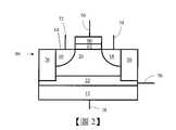
圖2和3示意性地示出了根據本發明實施例的記憶體格的截面圖。2 and 3 schematically show cross-sectional views of memory cells according to embodiments of the present invention.
圖4A是根據本發明另一實施例的記憶體格的示意性橫截面圖示。4A is a schematic cross-sectional illustration of a memory bank according to another embodiment of the present invention.
圖4B是圖4A中所示的記憶體格的示無性俯視圖。FIG. 4B is a schematic top view of the memory cell shown in FIG. 4A.
圖5A和5B是根據本發明實施例的具有鰭狀結構的記憶體格的示意性三維視圖。5A and 5B are schematic three-dimensional views of a memory cell with a fin structure according to an embodiment of the present invention.
圖6A是根據本發明實施例的具有鰭狀結構的記憶體格的示意性三維視圖。6A is a schematic three-dimensional view of a memory cell with a fin structure according to an embodiment of the present invention.
圖6B是根據本發明實施例的具有鰭狀結構的記憶體元陣列的示意性三維視圖。FIG. 6B is a schematic three-dimensional view of a memory cell array with a fin structure according to an embodiment of the present invention.
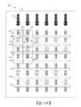
圖7示意性地示出了根據本發明實施例的圖6B中所示的記憶體陣列的佈局圖。FIG. 7 schematically shows a layout of the memory array shown in FIG. 6B according to an embodiment of the present invention.
圖8A和8B示意性地示出了根據本發明實施例的圖6B中所示的記憶體陣列的佈局圖。8A and 8B schematically illustrate the layout of the memory array shown in FIG. 6B according to an embodiment of the present invention.
圖9A和9B示意性地示出了根據本發明另一實施例的圖6B中所示的記憶體陣列的佈局。9A and 9B schematically illustrate the layout of the memory array shown in FIG. 6B according to another embodiment of the present invention.
圖10A和10B示意性地示出了根據本發明另一實施例的圖6B中所示的記憶體陣列的佈局圖。10A and 10B schematically illustrate the layout of the memory array shown in FIG. 6B according to another embodiment of the present invention.
圖11A和11B示意性地示出了根據本發明另一實施例的圖6B中所示的記憶體陣列的佈局圖。11A and 11B schematically illustrate the layout of the memory array shown in FIG. 6B according to another embodiment of the present invention.
圖12A和12B示意性地示出了根據本發明另一實施例的圖6B中所示的記憶體陣列的佈局圖。12A and 12B schematically illustrate the layout of the memory array shown in FIG. 6B according to another embodiment of the present invention.
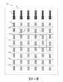
圖13是根據本發明實施例的具有鰭狀結構的記憶體格陣列的示意性三維視圖。FIG. 13 is a schematic three-dimensional view of a memory cell array with a fin structure according to an embodiment of the present invention.
圖14示意性地示出了根據本發明的實施例的圖13中所示的記憶體陣列的佈局圖。FIG. 14 schematically shows a layout of the memory array shown in FIG. 13 according to an embodiment of the present invention.
圖15A和15B示意性地示出了根據本發明另一實施例的圖13中所示的記憶體陣列的佈局圖。15A and 15B schematically illustrate the layout of the memory array shown in FIG. 13 according to another embodiment of the present invention.
圖16A和16B示意性地示出了根據本發明另一實施例的圖13中所示的記憶體陣列的佈局圖。16A and 16B schematically illustrate the layout of the memory array shown in FIG. 13 according to another embodiment of the present invention.
圖17示意性地示出了根據本發明另一實施例的記憶體陣列的佈局圖。FIG. 17 schematically shows a layout diagram of a memory array according to another embodiment of the present invention.
圖18是根據本發明的實施例的記憶體格的示意性橫截面圖示。Figure 18 is a schematic cross-sectional illustration of a memory bank according to an embodiment of the invention.
圖19是根據本發明實施例的具有記憶體件和具有不同導電類型的存取電晶體的記憶體格的示意性橫截面圖示。19 is a schematic cross-sectional illustration of a memory cell having memory elements and access transistors of different conductivity types according to an embodiment of the present invention.
圖20是根據本發明實施例的具有鰭狀結構的記憶體格的示意性三維視圖。FIG. 20 is a schematic three-dimensional view of a memory cell having a fin structure according to an embodiment of the present invention.
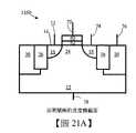
圖21A-21B是根據本發明另一實施例的記憶體格的示意性橫截面圖示。21A-21B are schematic cross-sectional illustrations of memory cells according to another embodiment of the present invention.
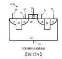
圖22A-22B是根據本發明另一實施例的記憶體格的示意性橫截面圖示。22A-22B are schematic cross-sectional illustrations of memory cells according to another embodiment of the present invention.
圖23A-23B示意性地示出了根據本發明實施例的由於施加到記憶體格的偏置條件而形成的空乏區。23A-23B schematically illustrate depletion regions formed due to bias conditions applied to memory cells, according to embodiments of the present invention.
圖24A-24B示意性地示出了根據本發明另一實施例的由於施加到記憶體格的偏置條件而形成的空乏區。24A-24B schematically illustrate depletion regions formed due to bias conditions applied to memory cells according to another embodiment of the present invention.
圖25是根據本發明另一實施例的具有記憶體件和具有不同導電類型的存取電晶體的記憶體格的示意性橫截面圖示。25 is a schematic cross-sectional illustration of a memory cell with memory elements and access transistors with different conductivity types according to another embodiment of the present invention.
圖26示意性地示出了根據本發明另一實施例的由於施加到記憶體格的偏置條件而形成的空乏區。Fig. 26 schematically shows another embodiment according to the present inventionThe depletion region formed due to the bias conditions applied to the memory cell.
圖27是示出根據本發明的實施例的記憶體件的操作的流程圖。FIG. 27 is a flowchart showing the operation of the memory device according to the embodiment of the present invention.
圖28示意性地示出了根據本發明實施例的記憶體格,其包括串聯連接的記憶體件和存取裝置,以及與記憶體件串聯連接的電阻改變元件。FIG. 28 schematically shows a memory cell according to an embodiment of the present invention, which includes a memory device and an access device connected in series, and a resistance changing element connected in series with the memory device.
圖29示意性地示出了根據本發明實施例的圖28的記憶體格的等效電路表示,其中記憶體設備是雙穩態浮體設備。Figure 29 schematically illustrates an equivalent circuit representation of the memory grid of Figure 28, in which the memory device is a bistable floating body device, according to an embodiment of the present invention.
圖30是根據本發明的實施例的記憶體格的示意圖。FIG. 30 is a schematic diagram of a memory bank according to an embodiment of the present invention.
圖31是根據本發明另一實施例的記憶體格的示意圖。FIG. 31 is a schematic diagram of a memory grid according to another embodiment of the present invention.
圖32示意性地示出了根據本發明實施例的圖29中所示類型的多個格被連接以製造記憶體陣列。Figure 32 schematically illustrates a plurality of grids of the type shown in Figure 29 being connected to fabricate a memory array in accordance with an embodiment of the present invention.
圖33示意性地示出了根據本發明實施例的對記憶體陣列的保持操作的性能。FIG. 33 schematically illustrates performance of a hold operation on a memory array according to an embodiment of the present invention.
圖34示出了根據本發明實施例的施加在所選記憶體格的端子上的偏置條件。FIG. 34 illustrates bias conditions applied to terminals of selected memory cells according to an embodiment of the invention.
圖35示意性地示出了根據本發明實施例的對記憶體陣列的遮蔽操作的性能。Figure 35 schematically illustrates the performance of a masking operation on a memory array according to an embodiment of the present invention.
圖36A-36B示出了根據本發明實施例的施加在所選記憶體格的端子上的偏置條件。36A-36B illustrate bias conditions applied to terminals of selected memory cells according to an embodiment of the present invention.
圖37示意性地示出了根據本發明實施例的記憶體陣列上的恢復操作的性能。Figure 37 schematically shows a record according to an embodiment of the present inventionperformance of restore operations on memory arrays.
圖38A-38C示出了根據本發明實施例的施加在所選記憶體格的端子上的偏置條件。38A-38C illustrate bias conditions applied to terminals of selected memory cells according to an embodiment of the present invention.
圖39示意性地示出了根據本發明實施例的記憶體陣列上的複位操作的性能。Figure 39 schematically illustrates the performance of a reset operation on a memory array according to an embodiment of the present invention.
圖40A-40B示出了根據本發明實施例的施加在所選記憶體格的端子上的偏置條件。40A-40B illustrate bias conditions applied to terminals of selected memory cells in accordance with an embodiment of the present invention.
圖41示意性地示出了圖1和圖2的記憶體格的等效電路表示。參照圖40A-40B,根據本發明的一個實施例。FIG. 41 schematically shows an equivalent circuit representation of the memory cells of FIGS. 1 and 2 . Referring to Figures 40A-40B, according to one embodiment of the present invention.
圖42示意性地示出了包括記憶體件和具有不同導電類型的串聯連接的存取裝置的記憶體格,和根據本發明的另一個實施例,電阻改變元件與記憶體件串聯連接。42 schematically shows a memory cell including memory elements and access devices having different conductivity types connected in series, and according to another embodiment of the present invention, a resistance changing element is connected in series with the memory elements.
圖43示意性地示出了包括記憶體件和具有不同導電類型的串聯連接的存取裝置的記憶體格,和根據本發明的另一個實施例,電阻改變元件與記憶體件串聯連接。43 schematically shows a memory cell including memory elements and access devices having different conductivity types connected in series, and according to another embodiment of the present invention, a resistance changing element is connected in series with the memory elements.
圖44示意性地示出了根據本發明實施例的由於施加到圖43的記憶體格的偏置條件而形成的空乏區。FIG. 44 schematically illustrates depletion regions formed due to bias conditions applied to the memory cells of FIG. 43 in accordance with an embodiment of the present invention.
圖45示意性地示出了具有三維鰭狀結構的記憶體格,並且其包括串聯連接的記憶體件和存取器件,以及與記憶體件串聯連接的電阻改變元件,根據本發明的另一個實施方案。Figure 45 schematically shows a memory grid with a three-dimensional fin structure, and it includes memory devices and access devices connected in series, and resistance changing elements connected in series with the memory devices, according to another implementation of the present invention plan.
在描述本發明記憶體格,陣列和方法之前,應理解本發明不限於所描述的特定實施例,因此當然可以改變。還應理解,本文使用的術語僅用於描述特定實施方案的目的,而不是限制性的,因為本發明的範圍僅受所附權利要求的限制。Before the present invention memory cells, arrays and methods are described, it is to be understood that this invention is not limited to particular embodiments described, as such may, of course, vary. It is also to be understood that the terminology used herein is for the purpose of describing particular embodiments only and is not limiting, since the scope of the present invention will be limited only by the appended claims.
在提供數值範圍的情況下,應當理解,除非上下文另有明確規定,否則還具體公開了該範圍的上限和下限之間的每個中間值,至下限單位的十分之一。在所述範圍內的任何規定值或介入值與所述範圍內的任何其他陳述或介入值之間的每個較小範圍都包含在本發明內。這些較小範圍的上限和下限可以獨立地包括在該範圍內或排除在該範圍內,並且在較小範圍中包括任一個,兩個或兩個限制的每個範圍也包括在本發明內,受制於本發明中的任何特別排除的限制。規定的範圍。在所述範圍包括一個或兩個限制的情況下,排除那些包括的限制之一或兩者的範圍也包括在本發明中。Where a range of values is provided, it is understood that unless the context clearly dictates otherwise, each intervening value between the upper and lower limits of that range, to the tenth of the unit of the lower limit, is also specifically disclosed. Each smaller range between any stated value or intervening value in a stated range and any other stated or intervening value in that stated range is encompassed within the invention. The upper and lower limits of these smaller ranges may independently be included in or excluded from that range, and where either is included in the smaller ranges, each range of both or both limits is also encompassed within the invention, subject to any specifically excluded limitations herein. specified range. Where the stated range includes one or both of the limits, ranges excluding either or both of those included limits are also included in the invention.
除非另有定義,本文使用的所有技術和科學術語具有與本發明所屬領域的普通技術人員通常理解的含義相同的含義。儘管與本文描述的那些類似或等同的任何方法和材料可用於本發明的實踐或測試,但現在描述優選的方法和材料。本文提及的所有出版物均通過引用併入本文,以公開和描述與所引用的出版物相關的方法和/或材料。Unless defined otherwise, all technical and scientific terms used herein have the same meaning as commonly understood by one of ordinary skill in the art to which this invention belongs. Although any methods and materials similar or equivalent to those described herein can be used in the practice or testing of the present invention, the preferred methods and materials are now described. All publications mentioned herein are incorporated herein by reference to disclose and describe the methods and/or materials in connection with which the publications are cited.material.
必須指出,如本文和所附權利要求中所使用的,單數形式“一”,“一個”和“該”包括複數指示物,除非上下文另有明確說明。因此,例如,對“記憶體格”的引用包括多個這樣的記憶體格,並且對“該區域”的引用包括對一個或多個區域的引用及其本領域技術人員已知的等同物,等等。It must be noted that as used herein and in the appended claims, the singular forms "a," "an," and "the" include plural referents unless the context clearly dictates otherwise. Thus, for example, reference to "a memory cell" includes a plurality of such memory cells and reference to "the region" includes reference to one or more regions and equivalents known to those skilled in the art, etc. .
提供本文討論的出版物僅僅是因為它們在本申請的提交日之前的公開內容。本文中的任何內容均不應被解釋為承認本發明無權憑藉在先發明而先於這些出版物。此外,提供的出版日期可能與可能需要獨立確認的實際出版日期不同。The publications discussed herein are provided solely for their disclosure prior to the filing date of the present application. Nothing herein should be construed as an admission that the present invention is not entitled to antedate these publications by virtue of prior invention. In addition, the dates of publication provided may differ from the actual publication dates which may need to be independently confirmed.
如本文所使用的短語“穩定浮體充電位準”或“穩定充電位準”是指浮體充電位準,其中註入浮體區域的空穴(或電子)的量(例如,通過碰撞游離機制產生的空穴的結果)補償浮體區域外的電荷損失(例如由於p-n結正向偏置電流或由於電荷複合)。As used herein, the phrase "stable buoy charge level" or "stable charge level" refers to the buoy charge level in which the amount of holes (or electrons) injected into the buoy region (e.g., by collision The result of holes generated by the dissociation mechanism) compensates for charge loss outside the floating body region (eg due to p-n junction forward bias current or due to charge recombination).
如本文所用,“雙穩態記憶體格”或“雙穩態”是指具有兩種穩定狀態的記憶體格。例如,雙穩態浮體記憶體格具有兩個穩定的浮體充電位準,其中註入浮體區域的空穴(或電子)的量補償浮體區域外的電荷損失(例如由於p-n結正向偏置電流或由於電荷重組)。As used herein, a "bistable memory cell" or "bistable" refers to a memory cell that has two stable states. For example, a bistable floating body memory cell has two stable floating body charge levels, where the amount of holes (or electrons) injected into the floating body region compensates for charge loss outside the floating body region (e.g. due to p-n junction forward bias current or due to charge recombination).
圖1示出了記憶體實例1200,其包括記憶體陣列100和與記憶體陣列100相關聯的外圍電路。外圍電路的例子如圖1所示:控制邏輯102接收例如使能(/E)和寫(/W)信號並控制記憶體陣列的操作;地址緩衝器110,其將接收到的地址發送到行解碼器112和列解碼器114;讀出電路,例如讀出放大器116和糾錯電路(ECC)118;數據緩衝器120,輸出讀數據或將寫數據發送到寫驅動器130;模擬電源發生器和/或調節器140,它們提供記憶體陣列操作所需的附加電壓電平;冗餘邏輯150,可用於增加記憶體實例的產量;內置自測試(BIST)160,其可用於設置供應發生器140的調整水平和/或用冗餘陣列替換缺陷格。BIST 160可以感測芯片溫度並根據溫度調整電源發生器的電壓電平。記憶體實例1200可以是分立記憶體組件,或者它可以嵌入在另一個集成電路器件1000內。FIG. 1 shows a
參考圖2,示出了根據本發明的實施例的記憶體格50。多個記憶體格50(或本文所述的任何其他記憶體格)可用於構成記憶體陣列100,如圖1所示。記憶體格50包括例如第一導電類型的襯底12,例如p型。襯底12通常由矽製成,但是也可以包括例如鍺,矽鍺,砷化鎵,碳納米管和/或其他半導體材料。在本發明的一些實施例中,襯底12可以是半導體晶片的塊狀材料。在圖3所示的另一個實施例中,第一導電類型(例如,p型)的襯底12A可以是嵌入第二導電類型的井29中的第一導電類型的井,例如n型。井29又可以是第一導電類型的襯底12B內的另一個井(例如,p型)。在另一個實施例中,井12A可以嵌入第二導電類型的半導體晶片的主體內(例如,n型)。這些佈置允許分割基板端子78,基板端子78連接到區域12A。為了簡化描述,通常將基板12拉成如圖2中的半導體塊材料。Referring to FIG. 2 , a
記憶體格50還包括第二導電類型的掩埋層區域22,例如n型;第一導電類型的浮體區24,例如p型;和第二導電類型的源/漏區16和18,例如n型。The
可以通過離子注入工藝在襯底12的材料上形成掩埋層22。或者,掩埋層22可以在襯底12的頂部外延生長,或者通過固態擴散工藝形成。The buried
第一導電類型的浮體區域24在頂部由源極線區域16,漏極區域18和絕緣層62(或通常由表面14)界定,在側面上由絕緣層26界定,並且在底部是埋層22。如果埋入層22被植入,則浮體24可以是掩埋層22上方的原始襯底12的部分。或者,浮體24可以外延生長。取決於如何形成掩埋層22和浮體24,在一些實施例中,浮體24可以具有與襯底12相同的摻雜或者如果在其他實施例中需要,可以具有不同的摻雜。The floating
具有第二導電類型(例如,n型)的源極線區域16設置在浮體區域24中,以便以上面討論的方式限制浮體區域的頂部的一部分。,並在表面14處暴露。根據本領域已知和通常使用的任何注入工藝,源極線區16可以通過注入工藝在構成基板12的材料上形成。或者,可以使用固態擴散或選擇性外延生長工藝來形成源極線區域16。A
在浮體區域24中提供具有第二導電類型(例如,n型)的位線區域18(也稱為漏極區域18),以便限制頂部的一部分以上述方式測量浮體區域,並暴露在細胞表面14處。根據本領域已知和通常使用的任何注入工藝,可以通過在構成襯底12的材料上的注入工藝來形成位線區域18。或者,可以使用固態擴散或選擇性外延生長工藝來形成位線區域18。A bitline region 18 (also referred to as drain region 18) of a second conductivity type (eg, n-type) is provided in the floating
閘極60位於浮置體區域24上方的源極線區域16和漏極區域18之間。閘極60通過絕緣層62與浮體區域24絕緣。絕緣層62可以由氧化矽和/或其他介電材料製成,包括高K介電材料,例如但不限於過氧化鉭,氧化鈦,氧化鋯,氧化鉿和/或氧化鋁。閘極60可以由例如多晶矽材料或金屬柵電極製成,例如鎢,鉭,鈦和它們的氮化物。
絕緣層26(例如,淺溝槽隔離(STI))可以由例如氧化矽製成,但是可以使用其他絕緣材料。絕緣層26使記憶體格50與相鄰的記憶體格50絕緣。絕緣層26的底部可以位於掩埋區域22內,允許掩埋區域22連續,如圖2和3所示。或者,記憶體件可具有兩個不同的絕緣層26和28(例如,淺溝槽隔離(STI)和深溝槽隔離(DTI)。如圖4A和4B所示,絕緣層26的底部可以位於掩埋區域22內,允許掩埋區域22在圖4A所示的橫截面圖的雙側方向上連續,而底部絕緣層28可以位於掩埋層22下方。The insulating layer 26 (eg, shallow trench isolation (STI)) may be made of, for example, silicon oxide, although other insulating materials may be used. The insulating
格50包括多個端子:字線(WL)端子70電連接到閘極60,位線(BL)端子74電連接到位線區域18,源極線(SL)端子72電連接到源極線區域如圖16所示,掩埋井(BW)端子76電連接到掩埋層22,並且襯底端子78電連接到襯底12。或者,SL端子72可以電連接到區域18,BL端子74可以電連接到區域16。
記憶體格50可以執行若干操作,例如保持,讀取,寫入邏輯1和寫入邏輯0操作,並且已經在Widjaja等人於美國專利申請9,230,651號,標題為“帶有電浮體電晶體的非對稱半導體記憶體器件”(“Widjaja-3”)中上述的一樣和美國專利8,077,536號,標題為“帶有浮體電晶體使用可控矽整流器原理的半導體記憶體件之操作方法”(“Widjaja-2”)中上述的一樣,它們完整引用於此。
圖5A和5B示出了根據本發明另一實施例的具有鰭狀結構的記憶體格50的示意性三維視圖。記憶體格50具有在諸如p型的第一導電類型的基板12上製造的鰭狀結構,以便從基板的表面延伸以形成三維結構,其中鰭片基本上垂直於上方延伸。基板12的頂表面。記憶體格50具有在諸如p型的第一導電類型的基板12上製造的鰭狀結構,以便從基板的表面延伸以形成三維結構,其中鰭片基本上垂直於上方延伸。基板12的頂表面。鰭狀結構是半導電的並且構建在第二導電類型的掩埋井層22上,例如n型,其本身構建在襯底12的頂部上。或者,掩埋井22可以是襯底12內部的擴散區域,其餘部分構造在其上方,或者掩埋井22可以是襯底12頂部上的導電層,以類似於記憶體的方式連接到所有其他鰭狀結構上述細胞50。鰭片通常由矽製成,但可包括鍺,矽鍺,砷化鎵,碳納米管或本領域已知的其他半導體材料。在其他實施例中,襯底12A可以是嵌入第二導電類型的井29中的第一導電類型的井,或者可選地,嵌入在第二導電類型的半導體晶片的主體中,例如n型,用於例如,如圖5B所示。為了簡化描述,通常將基板12拉成半導體塊材料,如圖5A所示。5A and 5B show schematic three-dimensional views of a
圖6A和6B分別示出了根據本發明另一實施例的具有鰭狀結構和記憶體格陣列100陣列的記憶體格50的示意性三維視圖。具有鰭狀結構的記憶體格50是圖1和2中所示的鰭型器件的示例。圖4A和4B。記憶體格50可以包括雙深度絕緣層;像淺溝槽隔離(STI)的絕緣層26和像深溝槽隔離(DTI)的絕緣層28。絕緣層26使記憶體格50與相鄰的記憶體格50絕緣。絕緣層26的底部位於掩埋區域22內,允許掩埋區域22連續,如圖6B所示。絕緣層28的底部位於掩埋層22下方。結果,掩埋層22沿溝道長度方向變得連續,但沿著閘極60方向電去耦,使得沿溝道長度方向的每個掩埋層可以具有獨立的偏置。6A and 6B respectively show schematic three-dimensional views of a
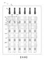
圖7示出了根據本發明另一實施例的記憶體陣列100的佈局圖。記憶體陣列100位於掩埋井區170內。記憶體陣列100包括位於場氧化物區域上的附加虛設POLY層160D。在另一個實施例中,每個場區域(未示出)可以使用兩個虛設POLY層160D。對於雙虛設POLY層的情況,虛設POLY層可以部分地覆蓋DIFF區域130。虛設層160D例如可以是限制性設計規則(其引導層的佈局圖)的結果,以用於更好的光刻圖案化過程。為了簡化描述,通常在下文中如圖7中那樣繪製單個虛設POLY層160D。DIFF層130限定記憶體格的有源區(圖4A中的橫截面圖中所示的絕緣層26和28之間的區域)。或者,DIFF層130可以限定記憶體格50的鰭片.DIFF層130可以通過兩步驟工藝形成。心軸層是長線圖案,其中心軸層之間的層限定絕緣層28,例如深溝槽隔離。然後,接著進行鰭片切割層,其中鰭片切割層之間的層限定絕緣層26,例如淺溝槽隔離。POLY層160和虛設POLY層160D限定了圖4A的橫截面圖中所示的閘極區60。如圖7所示,記憶體格50的單位格包括兩個POLY160區域;一個160D用於限定虛設區域,另一個160用於限定與DIFF層130完全重疊的電晶體區域。POLY 160和DIFF 130層之間的重疊形成記憶體格50的溝道區,例如閘極區60和介電層62下方的區域,位於圖2中所示的源極線區16和位線區18之間。記憶體陣列100可以包括掩埋井層抽頭180。掩埋井層抽頭180形成在DIFF 130層上,而其可以摻雜第二導電類型,例如n型,與掩埋層區域22相同。掩埋井層抽頭180形成在記憶體陣列100或記憶體子陣列100的周邊處,例如陣列的頂部或底部。每個掩埋井層抽頭180連接到其自己的掩埋層22,並且通過相應的掩埋井層抽頭180獨立地控制掩埋層22的電壓。FIG. 7 shows a layout diagram of a
根據本發明的一個實施例,如圖7所示的記憶體格陣列100被配置用於由兩個電晶體組成的格記憶體格;一個用於浮體記憶體格電晶體,一個用於非浮體存取電晶體,通過基於雙深度絕緣層技術的獨立掩埋井偏置方案,如圖4A-4B和圖6A-6B所示。According to one embodiment of the present invention, the
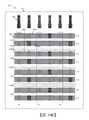
圖8A和8B示出了來自圖7的記憶體陣列100的記憶體陣列400的佈局圖,示出了關於如何為雙電晶體格記憶體格450形成與源極線區域16和位線區域18的電性接觸的示例。雙電晶體格記憶體格450包括記憶體件450M和存取器件450A,它們串聯連接,美國專利申請號為14/380,779,標題為“包括第一和第二電晶體和操作方法的記憶體格”(“Widjaja-4”)中所描述一樣,其全部內容通過引用結合於此。8A and 8B show layout views of
記憶體件450M和存取裝置450A都是在掩埋層170上找到的電晶體。CONT-A 140A層可用於形成與DIFF區域的連接,例如,記憶體件450M的漏極區域18和DIFF區域,例如通過導電METAL1層190A的存取裝置450A的源區16,例如金屬層。接下來,如圖8B所示,存取裝置450A的漏極區域18和記憶體裝置450M的源極區域16可以通過另一導電層172/174,172/174(例如METAL2層)連接到VIA層140B,其中導電層172和導電層174可互換地是記憶體陣列400的源極線和位線。Both
圖9A和9B示出了來自圖7的記憶體陣列100的記憶體陣列400的佈局圖,根據本發明另一實施例的關於如何為雙電晶體單位存儲格450形成與源極線區16和位線區18的電性接觸的示例。該實施例類似於圖8A-8B的實施例,除了記憶體裝置450M和存取裝置450A之間的連接190A以交錯方式製成之外。CONT-A 140A層可用於通過導電METAL1層190A形成與DIFF區域(例如記憶體件450M的漏極區域18)和DIFF區域(例如存取器件450A的源極區域16)的連接,例如,如圖9A所示的金屬層。接下來,如圖9B所示,存取裝置450A的漏極區域18和記憶體裝置450M的源極區域16然後可以通過另一導電層172/174,174/172(例如METAL2層)連接到VIA層140B,其中導電層172和導電層174可互換地是記憶體陣列400的源極線和位線。9A and 9B show layout diagrams of the
圖8A-9B中示出的示例性記憶體陣列400包括可互換源極線172和位線174,其中源極線172和位線174平行佈置。The
圖10A和10B示出了來自圖7的記憶體陣列100的記憶體陣列400的佈局圖,圖示了根據本發明另一實施例的關於如何為雙電晶體單位存儲格450形成與源極線區16和位線區18的電性接觸的示例。該實施例類似於圖8A-8B的實施例,除了源極線172和位線174沿彼此正交的方向排列之外。CONT-A 140A層可用於通過導電METAL1層190A形成與DIFF區域(例如記憶體件450M的漏極區域18)和DIFF區域(例如存取器件450A的源極區域16)的連接,例如,金屬層,如圖10A所示。接下來,接入裝置450A的漏極區域18然後可以通過VIA層140B連接到用於位線(例如METAL2層)的另一導電層174。10A and 10B show layout diagrams of
圖8A-10B中示出的示例性記憶體格450包括具有相同導電類型的兩個電晶體(450M和450A),例如,兩個串聯連接的n溝道電晶體,其中記憶體件450M和存取器件450A都是位於掩埋井層170內的電晶體。然而,由於連接到相應的掩埋井層抽頭180的獨立電壓可控掩埋井層170,記憶體件450M和存取器件450A可具有不同的掩埋井層170電壓。連接到記憶體件450M的掩埋井的掩埋井層抽頭180可以具有正偏置以在記憶體件450M中形成浮體,而連接到存取器件450A的掩埋井的掩埋井層抽頭180可以具有零或者諸如-0.1V的輕微負偏壓以在存取裝置450A中形成非浮體。The
圖8A-10B中所示的示例性記憶體格450包括對於記憶體件450M和存取裝置450A共同的字線160。在本發明的另一個實施例中,存儲格陣列被配置用於由兩個電晶體組成的格存儲格,用於浮體存儲電晶體的存儲格字線和用於非浮體存取電晶體的存取選擇字線,通過獨立的掩埋井偏置方案基於雙深度絕緣層技術。The
圖11A和11B示出了來自圖7的記憶體陣列100的記憶體陣列800的佈局圖,示出了關於如何為四電晶體格存儲格850形成與源極線區域16和位線區域18的電性接觸的示例。四電晶體格存儲格850包括串聯連接的記憶體件850M和存取器件850A,以及兩個虛設備850D,它們不與任何端子連接。所有記憶體件850M,存取裝置850A和虛設備850D是在掩埋層170上找到的電晶體。CONT-A 140A層可用於通過導電METAL1層190A形成與DIFF區域(例如記憶體件850M的漏極區域18)和DIFF區域(例如存取器件850A的源極區域16)的連接,用於示例金屬層。接下來,如圖11B所示,存取裝置850A的漏極區域18和記憶體裝置850M的源極區域16然後可以通過另一導電層172/174,174/172(例如METAL2層)連接到VIA層140B,其中導電層172和導電層174可互換地是記憶體陣列800的源極線和位線。11A and 11B show layout views of
圖11A-11中示出的示例性記憶體陣列800包括可互換源極線172和位線174,其中源極線172和位線174並聯佈置。The
圖12A和12B示出了來自圖7的記憶體陣列100的記憶體陣列800的佈局圖,示出了根據本發明另一實施例的關於如何為四線晶體格存儲格850形成與源極線區16和位線區18的電性接觸的示例。該實施例類似於圖11A-11B所示的類似除了源極線172和位線174彼此正交的方向排列之外。CONT-A 140A層可用於通過導電METAL1層190A形成與DIFF區域(例如記憶體件850M的漏極區域18)和DIFF區域(例如存取器件850A的源極區域16)的連接,用於示例金屬層如圖12A所示。接下來,接入裝置850A的漏極區域18然後可以通過VIA層140B連接到用於位線(例如METAL2層)的另一導電層174。接下來,如圖12B所示,記憶體件850M的源極區16可以通過VIA層140C連接到用於源極線(例如METAL3層)的另一導電層172。12A and 12B show layout diagrams of
圖11A-12B中所示的示例性記憶體格850包括具有相同導電類型的四個電晶體(850M,850A和850D),例如串聯連接的兩個n溝道電晶體,其中所有記憶體件850M,存取器件850A和虛設備850D是電晶體位於掩埋井層170上方(或在圖11A-12B所示的佈局圖中的掩埋井層170內)。然而,由於連接到相應的掩埋井層抽頭180的獨立電壓可控掩埋井層170,記憶體件850M和存取器件850A可具有不同的掩埋井層170電壓。連接到記憶體件850M的掩埋井的掩埋井層抽頭180可以具有正偏置以在記憶體件850M中形成浮體,而連接到存取器件850A的掩埋井的掩埋井層抽頭180可以具有零或者諸如-0.1V的輕微負偏壓以在存取裝置850A中形成非浮體。The
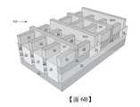
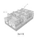
圖13示出了根據本發明另一實施例的記憶體格陣列300的示意性三維視圖。具有鰭狀結構的記憶體格50是圖4A和4B中所示的鰭型器件的示例。鰭片結構以交錯的方式佈置,使得相鄰格的鰭片偏移並且彼此不對齊,如圖13所示。本文描述的任何其他記憶體格的鰭狀結構也可以以圖13中所示的交錯方式佈置。記憶體格50可以包括雙深度絕緣層;像淺溝槽隔離(STI)的絕緣層26和像深溝槽隔離(DTI)的絕緣層28。絕緣層26使記憶體格50與相鄰的記憶體格50絕緣。絕緣層26的底部位於掩埋區域22內,允許掩埋區域22連續,如圖13所示。絕緣層28的底部位於掩埋層22下方。結果,掩埋層22沿溝道長度方向變得連續,但沿著閘極60方向電去耦,使得沿溝道長度方向的每個掩埋層可以具有獨立的偏置。FIG. 13 shows a schematic three-dimensional view of a
圖14示出了根據本發明另一實施例的記憶體陣列300的佈局圖。記憶體陣列300位於掩埋井區170內。DIFF層130限定記憶體格的有源區(圖4A中的橫截面圖中所示的絕緣層26和28之間的區域)。或者,DIFF層130可以限定記憶體格50的鰭片。DIFF層130以交錯的方式佈置,使得它們不沿著POLY 160延伸的方向對齊。因此,記憶體陣列300中的POLY層160僅在與DIFF層130重疊或交叉的區域中形成閘極60。DIFF層130可以通過兩步工藝形成。心軸層是長線圖案,其中心軸層之間的層限定絕緣層28,例如深溝槽隔離。然後,接著進行鰭片切割層,其中鰭片切割層之間的層限定絕緣層26,例如淺溝槽隔離。POLY層160限定了圖4A的橫截面圖中所示的閘極區域60。記憶體格50的晶胞包括兩個POLY160區域;一個POLY區域160用於限定電晶體區域,例如存儲電晶體,與DIFF層130和另一個POLY區域160完全重疊,以限定另一個電晶體區域,例如存取電晶體,與另一個DIFF層130完全重疊。POLY 160和DIFF 130層之間的重疊形成存儲電晶體和存取電晶體的溝道區,例如圖2中所示的源極線區16和位線區18之間的閘極區60和介電層62下方的區域。記憶體陣列300可以包括掩埋井層抽頭180。掩埋井層抽頭180形成在DIFF 130層上,而它可以摻雜第二導電類型,例如n型,與掩埋層區域22相同。掩埋井層抽頭180圍繞記憶體陣列300或記憶體子陣列300的周邊形成,例如在陣列的頂部或底部。每個掩埋井層抽頭180連接到其自己的掩埋層22部分,並且通過相應的掩埋井層抽頭180獨立地控制掩埋層22的電壓。Figure 14 shows a memory according to another embodiment of the present inventionLayout diagram of
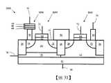
圖15A和15B示出了來自圖14的記憶體陣列300的記憶體陣列900的佈局圖,示出了關於如何為雙電晶體格記憶體格950形成與源極線區域16和位線區域18的電性接觸的示例。雙電晶體格存儲格950包括記憶體件950M和存取器件950A,它們串聯連接,美國專利申14/380,779號,標題為“包括第一和第二電晶體和操作方法的記憶體格”(“Widjaja-4”)中所描述一樣,其全部內容通過引用結合於此。記憶體件950M和存取器件950A都是在掩埋層170上(或在圖15A-15B所示的佈局圖中的掩埋層170內)形成的電晶體。CONT-A 140A層可用於通過導電METAL1層190A形成與DIFF區域(例如記憶體件950M的漏極區域18)和DIFF區域(例如存取器件950A的源極區域16)的連接,用於示例金屬層。接下來,如圖15B所示,接入裝置950A的漏極區域18和記憶體裝置950M的源極區域16然後可以通過另一導電層172/174,174/172(例如METAL2層)連接到VIA層140B,其中導電層172和導電層174可互換地是記憶體陣列900的源極線和位線。15A and 15B show layout views of
圖16A和16B示出了來自圖14的記憶體陣列300的記憶體陣列900的佈局圖,示出了根據另一實施例的關於如何為雙電晶體格記憶體格950形成與源極線區域16和位線區域18的電性接觸的示例。除了源極線172和位線174彼此正交地佈置之外,該實施例類似於圖15A-15B的實施例。CONT-A 140A層可用於通過導電METAL1層190A形成與DIFF區域(例如記憶體件950M的漏極區域18)和DIFF區域(例如存取器件950A的源極區域16)的連接,用於示例金屬層如圖16A所示。接下來,接入裝置950A的漏極區域18然後可以通過VIA層140B連接到用於位線(例如METAL2層)的另一導電層174。接下來,如圖16B所示,記憶體件950M的源極區16可以通過VIA層140C連接到用於源極線(例如METAL3層)的另一導電層172。16A and 16B show layout views of
圖15A-16B中示出的示例性記憶體格950包括:具有相同導電類型的兩個電晶體(950M和950A),例如串聯連接的兩個n溝道電晶體,其中記憶體件950M和存取器件950A都是位於掩埋井層170內的電晶體,如圖所示在圖15A-16B中的佈局視圖中。然而,由於連接到相應的掩埋井層抽頭180的獨立電壓可控掩埋井層170,記憶體件950M和存取器件950A可以具有不同的掩埋井層170電壓。連接到記憶體件950M的掩埋井的掩埋井層抽頭180可以具有正偏置以在記憶體件950M中形成浮體,而連接到接入器件950A的掩埋井的掩埋井層抽頭180可以具有零或者諸如-0.1V的輕微負偏壓以在存取裝置950A中形成非浮體。The
圖17示出了根據本發明另一實施例的記憶體陣列1000。在記憶體陣列1000中,記憶體格1050M和存取裝置1050A的閘極區域例如使用POLYCUT層160C分離。然後可以使用CONT-P 140P層來形成到記憶體件1050M和存取裝置1050A的閘極區域的連接,然後可以通過導電層(例如METAL1層(未示出))電連接。FIG. 17 shows a
圖18示出了根據本發明實施例的記憶體格1150。記憶體格1150的掩埋層區域22位於絕緣區域26下方。記憶體格1150的浮體區域24除了由16,62,18,26和22界定之外還受相鄰井區域的限制。例如,第二導電類型可以是20,例如n型。記憶體格1150的浮體區域24可以由浮體區域24的四個側面或者沿著溝道長度方向的兩個側面(即,沿著區域16和18的方向)由第二導電類型的相鄰井區域20界定,沿著繪圖平面)或垂直於浮體區域24的溝道長度方向的兩側(即垂直於由區域16和18限定的方向,進入繪圖平面)。FIG. 18 shows a
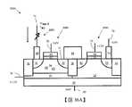
記憶體格1150的操作類似於記憶體格50的操作,例如在Widjaja-1,Widjaja-2和Widjaja-3中所描述的。對於記憶體格1150施加到掩埋層區域22(通過BW端子76,經由井區域20)的反偏壓可以比記憶體格50更高,因由源/漏區16和18形成的垂直雙極器件的基極區,浮體區24和掩埋層22對於存儲格1150而言比存儲格50的寬。The operation of the
圖19示出了根據本發明另一實施例的記憶體格1250。記憶體格1250包括記憶體裝置40和存取電晶體42’。圖19還示出了另一個記憶體格1250的一部分,其中僅示出了存取電晶體42’。因此,記憶體格1250的浮體區24部分地由存取電晶體42’的相鄰井區20和另一相鄰記憶體格1250的存取電晶體42’的相鄰井區20界定。記憶體件40包括具有多於一個穩定狀態的浮體區24。類似於記憶體格1150,記憶體格1250的記憶體裝置40包括位於絕緣區域26下方的掩埋層區域22。FIG. 19 shows a
存取電晶體42’具有與記憶體件40不同的導電類型。例如,記憶體件40可以是n型電晶體,存取電晶體42’可以是p型電晶體。存取電晶體42’包括第二導電類型的井區20,例如第一導電類型的n型源區16’和漏區18’,例如p型。第二導電類型的井區20電連接到掩埋井區22,因此不浮動。記憶體件40的浮體區24部分地由存取電晶體42’的井區20界定。The access transistor 42' has a different conductivity type than the
存取電晶體42’還包括位於源區16’和漏區18’之間的閘極64。絕緣層66可以由氧化矽和/或其他介電材料製成,包括高K介電材料,例如但不限於過氧化鉭,氧化鈦,氧化鋯,氧化鉿和/或氧化鋁。閘極64可以由例如多晶矽材料或金屬柵電極製成,例如鎢,鉭,鈦和它們的氮化物。Access transistor 42' also includes
具有記憶體件和存取電晶體的記憶體格1250的操作已在例如美國專利申請公開2015/0023105號,標題為“包括第一和第二電晶體和操作方法的記憶體格”中所描述一樣,其全部內容通過引用結合於此。Operation of a
在根據本發明的另一個實施例中,記憶體格1150和1250也可以以三維鰭狀結構形成。圖20示出了形成在鰭狀結構52中的存儲格1250F。圖20還示出了存儲格1250F,其中記憶體件40和存取電晶體42’在I-I’方向上(沿著繪圖平面)以交替模式排列。並且在I-I’方向(垂直於繪圖平面,即進入圖紙的頁面)。在根據本發明的另一個實施例中,記憶體件40和存取電晶體42’可以僅在一個方向上交替佈置,例如I-I’方向(沿著繪圖平面),其中沿著II“方向的行(進入繪圖平面)將包括所有記憶體設備40或所有存取電晶體42’。In another embodiment according to the present invention, the
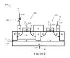
圖21A-21B示出了根據本發明另一實施例的記憶體格1350。記憶體格1350的體區24也由第二導電類型的井區20界定,例如n型。井區20可以沿著閘極寬度方向僅形成在兩側。然而,記憶體格1350的體區24在底部沒有被掩埋層區域物理限制。如圖21A-21B所示,在沒有施加到記憶體格1350的電壓偏置的情況下,記憶體格1350的體區24電連接到襯底區12。21A-21B illustrate a
圖22A-22B示出了根據本發明另一實施例的記憶體格1350。記憶體格1350的體區24也部分地由第二導電類型的井區20界定,例如n型。井區20可以沿閘極長度方向僅形成在兩側,如圖22B所示。然而,記憶體格1350的體區24在底部沒有被掩埋層區域物理限制。如圖22A-22B所示,在沒有施加到記憶體格1350的電壓偏置的情況下,記憶體格1350的體區24電連接到襯底區12。22A-22B illustrate a
如圖23A-24B所示,在向井區20(通過端子76)施加反偏壓時,在體區24和井區20的結中形成空乏區23(以虛線包圍)。應該理解的是,圖1和圖2中所示的空乏區邊界的形狀可以包括在內。圖23A-24B僅用於說明目的。相反,應該理解,它概念性地示出了來自左和右井區域20的耗盡邊界合併並且導致主體24浮動。由於反向偏置的p-n結,空乏區23可以延伸到體區24中,並且形成體區24的隔離。因此,記憶體格1350的體區24現在是浮動的,並且現在與相鄰的記憶體格1350的體區域隔離。主體區域24現在形成可以存儲電荷的勢井。空乏區形成體區24的隔離的記憶體格1350的操作已經在例如美國專利申請公開9,029,922,號,標題為”包含電浮體電晶體的記憶體件”中所描述一樣,其全部內容通過引用結合於此。As shown in FIGS. 23A-24B , upon application of a reverse bias voltage to the well region 20 (via terminal 76 ), a depletion region 23 (enclosed by a dashed line) is formed in the junction of the
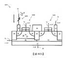
圖25示出了根據本發明另一實施例的記憶體格1450。記憶體格1450包括記憶體器件40和具有不同導電類型的存取電晶體42’。圖25還示出了另一個記憶體格1450的一部分,其中僅示出了存取電晶體42’。記憶體格1450的體區24部分地由第二導電類型的井區20界定,例如n型。然而,記憶體格1450的體區24在底部不被掩埋層區域界定。如圖25所示,在沒有施加到記憶體格1450的電壓偏置的情況下,記憶體格1350的體區24電連接到襯底區12。FIG. 25 shows a
如圖26所示,在向井區20(通過端子76)施加反偏壓時,在體區24和井區20的結中形成空乏區23(包圍在虛線中)。因此,記憶體格1450的體區24現在是浮動的並且現在與相鄰的記憶體格1450的體區域隔離。體區24現在形成可以存儲電荷的勢井。As shown in FIG. 26 , upon application of a reverse bias voltage to the well region 20 (via terminal 76 ), a depletion region 23 (enclosed in dashed line) is formed in the junction of the
圖27是示出根據本發明的記憶體件的操作的流程圖2100。在事件102處,當首次向記憶體設備供電時,記憶體設備處於初始狀態,處於揮發性操作模式,並且非揮發性記憶體被設置為預定狀態。在事件104處,記憶體設備以與揮發性記憶體相同的方式操作,例如作為SRAM或DRAM記憶體格。然而,在電源關閉期間,或者當電力意外丟失或者任何其他中斷或擾亂記憶體設備的電源的事件時,在參考的過程期間,在事件106處將揮發性記憶體的內容加載到非揮發性記憶體中。這裡稱為“陰影”(事件106),並且揮發性記憶體中保存的數據丟失。陰影可以在備份操作期間執行,其可以在揮發性操作104時段期間和/或在用戶手動指示備份的任何時間以規則間隔執行。在備份操作期間,揮發性記憶體的內容被複製到非揮發性記憶體,同時保持對揮發性記憶體的供電,使得揮發性記憶體的內容也保留在揮發性記憶體中。或者,因為揮發性記憶體操作比揮發性記憶體的內容的非揮發性存儲消耗更多的功率,所以該設備可以被配置為在設備已經空閒至少預定的時間段的任何時間執行陰影處理,從而將揮發性記憶體的內容傳送到非揮發性記憶體中並節省電力。作為一個示例,預定時間段可以是大約30秒,但是當然,本發明不限於該時間段,因為可以在幾乎任何預定時間段內對設備進行編程。FIG. 27 is a
在異常操作期間揮發性記憶體的內容已經移動到非揮發性記憶體之後,發生記憶體設備的關閉,因為不再向揮發性記憶體供電。此時,記憶體件將存儲的數據保存在非揮發性記憶體中。在事件108恢復供電時,通過在此處稱為“恢復”過程的過程中將非揮發性記憶體的內容傳送到揮發性記憶體來恢復非揮發性記憶體的內容,之後,在重置記憶體設備時在事件110處,記憶體設備可以被重置為初始狀態(事件102)並且再次以揮發性模式操作,如SRAM或DRAM記憶體設備,事件104。Shutdown of the memory device occurs after the contents of the volatile memory have been moved to the non-volatile memory during abnormal operation because power is no longer being supplied to the volatile memory. At this time, the memory component saves the stored data in the non-volatile memory. When power is restored at
圖28示出了根據本發明實施例的記憶體格2050的說明性非排他性示例。格2050包括串聯連接的存取裝置2050A和存儲裝置2050M,例如在Widjaja-4中所描述的,其在此通過引用整體併入本文,以及存儲格450,850,300,950,根據本發明的實施例的1250,1250F,1450;電阻改變元件2090串聯連接到記憶體件2050M。記憶體裝置2050M用於將記憶體格2050的狀態存儲在揮發性記憶體操作模式中,並且通過存取裝置2050A存取,而電阻改變元件2090用於將記憶體格2050的存儲狀態在非揮發性記憶體操作模式中。Figure 28 shows an illustrative, non-exclusive example of a
圖29示出了根據本發明實施例的記憶體格2050的等效電路表示,其中記憶體件2050M是雙穩態浮體裝置,例如Widjaja-1,Widjaja-2中所述,和Widjaja-3,以及根據本發明實施例的記憶體格50,1150,1350,並且其中存取裝置2050A是金屬氧化物半導體(MOS)電晶體。Figure 29 shows an equivalent circuit representation of a
圖30中示出了根據本發明的實施例的記憶體格2050的示意性剖視圖。記憶體格2050包括兩個電晶體:具有電晶體2040的記憶體件2050M,其具有電浮置體24和具有存取電晶體2042的存取裝置2050A。記憶體格2050包括例如第一導電類型的襯底10,例如p型。襯底10通常由矽製成,但也可包括例如鍺,矽鍺,砷化鎵,碳納米管或其他半導體材料。在本發明的一些實施例中,襯底10可以是半導體晶片的塊狀材料。在其他實施例中,襯底10可以是嵌入第二導電類型的井中的第一導電類型的井,或者可選地,嵌入在第二導電類型的半導體晶片的主體中,例如n型,(在圖中未示出)。作為設計選擇的問題。為了簡化描述,通常將襯底10繪製為如圖30中的半導體塊狀材料。A schematic cross-sectional view of a
浮體電晶體2040還包括第二導電類型的掩埋層區域30,例如n型;第一導電類型的浮體區24,例如p型;和第二導電類型的源/漏區16和18,例如n型。The floating
可以通過離子注入工藝在襯底10的材料上形成掩埋層30.或者,可以在襯底10的頂部外延生長掩埋層30。The buried
第一導電類型的浮體區域24在頂部由表面14,源極線區域16,漏極區域18和絕緣層62界定,在側面上由絕緣層26界定,並且在底部由埋層層界定30。如果埋入層30被植入,則浮體24可以是掩埋層30上方的原始襯底10的部分。或者,浮體24可以外延生長。取決於如何形成掩埋層30和浮體24,在一些實施例中,浮體24可以具有與襯底10相同的摻雜或者如果在其他實施例中需要,可以具有不同的摻雜。The floating
閘極60位於浮置體區域24上方的源極線區域16和漏極區域18之間。閘極60通過絕緣層62與浮體區域24絕緣。絕緣層62可以由氧化矽和/或其他電介質材料製成,包括高K電介質材料,例如但不限於過氧化鉭,氧化鈦,氧化鋯,氧化鉿和/或氧化鋁。閘極60可以由例如多晶矽材料或金屬柵電極製成,例如鎢,鉭,鈦和它們的氮化物。
絕緣層26(例如,淺溝槽隔離(STI))可以由氧化矽製成,但是可以使用其他絕緣材料。絕緣層26使浮體電晶體2040與相鄰的浮體電晶體2040和相鄰的存取電晶體2042絕緣。絕緣層26的底部可以位於掩埋區域30內,允許掩埋區域30連續,如圖30所示。或者,絕緣層26的底部可以位於掩埋區域30下方。這需要較淺的絕緣層28,其使浮體區域24絕緣,但允許埋層30在圖30所示的橫截面圖的垂直方向上連續。為簡單起見,將僅示出在所有方向上具有連續掩埋區域30的記憶體格2050。The insulating layer 26 (eg, shallow trench isolation (STI)) may be made of silicon oxide, although other insulating materials may be used. The insulating
存取電晶體2042包括第一導電類型的井區12,例如p型,源區20和第二導電類型的位線區22,例如n型。第一導電類型的井區12電連接到襯底區10,因此不浮動。閘極64位於源極區20和位線區22之間。閘極64通過絕緣層66與井區12絕緣。絕緣層66可以由氧化矽和/或其他介電材料製成,包括高K介電材料,例如但不限於過氧化鉭,氧化鈦,氧化鋯,氧化鉿和/或氧化鋁。閘極64可以由例如多晶矽材料或金屬柵電極製成,例如鎢,鉭,鈦和它們的氮化物。The
浮體電晶體2040的漏極區18通過導電元件94連接到存取電晶體2042的源極區20。導電元件90將浮體電晶體2040的源極線區域16(可以互換地稱為記憶體件50的源極線區域16)連接到電阻改變元件2090,電阻改變元件2090又連接到源極線(SL)終端74。導電元件92將存取電晶體2042的位線區域22(可以互換地稱為記憶體件2050的位線區域22)連接到位線(BL)端子76.導電元件90,92和94可以由,但不限於,鎢或矽化矽形成。The
圖31中示出了記憶體格2050的非限制性實施例。該實施例中的電阻改變記憶體元件2090包括底部電極44,電阻改變材料46和頂部電極48。A non-limiting example of a
圖31中示出了記憶體格2050的非限制性實施例。該實施例中的電阻改變記憶體元件2090包括底部電極44,電阻改變材料46和頂部電極48。電阻改變存儲元件2090通過導電元件90連接到基板12上的第二導電區域16。電阻改變材料46可以通過由導電材料形成的電極48連接到地址線(例如圖31中的SL端子74)。導電元件90可以包括鎢或矽化矽材料。電極44,48可以由一種或多種導電材料形成,包括但不限於氮化鈦,氮化鈦鋁或氮化鈦矽。電阻改變材料46是可以使用電信號修改諸如電阻的特性的材料。A non-limiting example of a
對於相變存儲元件的情況,電阻率取決於材料的晶相,而對於金屬氧化物材料,電阻率通常取決於導電細絲的存在或不存在。相變型電阻改變材料的晶相表現出低電阻率(例如~1kΩ)狀態,並且該材料的非晶相表現出高電阻率狀態(例如>100kΩ)。相變材料的實例包括含有元素週期表第VI列元素的合金,例如GeSbTe合金。金屬-絕緣體-金屬電阻改變材料的實例包括各種氧化物,如Nb2O5,Al2O3,Ta2O5,TiO2和NiO,以及鈣鈦礦金屬氧化物,如SrZrO3,(PrCa)MnO3和SrTiO3:Cr。In the case of phase-change memory elements, the resistivity depends on the crystalline phase of the material, while for metal oxide materials, the resistivity typically depends on the presence or absence of conductive filaments. The crystalline phase of the phase-change resistance-altering material exhibits a low-resistivity (eg, ~1 kΩ) state, and the amorphous phase of the material exhibits a high-resistivity state (eg, >100 kΩ). Examples of phase change materials include alloys containing elements of column VI of the periodic table, such as GeSbTe alloys. Metal-Examples of insulator-metal resistance changing materials include various oxides such as Nb2O5, Al2O3, Ta2O5, TiO2 and NiO, and perovskite metal oxides such as SrZrO3, (PrCa)MnO3 and SrTiO3:Cr.
電阻改變材料46也可以由雙極電阻存儲元件形成,例如過渡金屬氧化物,鐵電,鐵磁材料,磁阻和/或自旋轉移扭矩磁性材料。雙極電阻存儲元件的電阻率狀態取決於跨越雙極電阻存儲元件的電位差或電流的極性。The resistance-altering material 46 may also be formed from bipolar resistive memory elements, such as transition metal oxides, ferroelectric, ferromagnetic materials, magnetoresistive and/or spin-transfer torque magnetic materials. The resistivity state of a bipolar resistive memory element depends on the polarity of the potential difference or current across the bipolar resistive memory element.
電阻改變存儲元件2090電連接到浮體電晶體2040,浮體電晶體2040包括第一區域16,浮體區域24,第二區域18和柵電極60。揮發性記憶體(即浮體電晶體2040)和非揮發性記憶體(即電阻改變存儲元件2090)之間的間隔距離可以很小,例如從大約90nm到大約1μm,優選從大約90nm到大約90nm。如果電阻改變元件2090位於表面14和最底部(或第一)金屬層之間用於28-nm技術,則為500nm,更優選地為約90nm至約100nm,或者如果電阻改變元件2090,則小於1um。用於28nm技術工藝的第四金屬層位於第四金屬層下方,或者小於10um,這取決於例如在其上實現可尋址線(例如,源極線74)的哪個金屬層,以及工藝技術節點。The resistance
除了SL端子74和BL端子76之外,記憶體格2050還包括字線1(WL1)端子70,其電連接到浮體電晶體2040的閘極60,字線2(WL2)端子72,其電連接到存取電晶體2042的閘極64,掩埋井(BW)端子78,其電連接到浮體電晶體2040的掩埋井區域30,以及襯底(SUB)端子80,其與基板區域10連接。In addition to
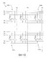
圖32中示出了包括以行和列佈置的多個記憶體格2050的記憶體陣列2120(作為圖28中所示的記憶體格2050的示例性實施方式)。圖32示出了標記為2050a,2050b,2050c和2050d的記憶體格2050的四個示例性實例。在示例性陣列2120出現的許多但不是全部的圖中,當所描述的操作具有一個(或多個在一些實施例中)選定的記憶體格2050時,代表性記憶體格2050a將代表“選定的”記憶體格2050。這些圖中,代表性記憶體格2050b將代表與所選代表性記憶體格2050a共享相同行的未選擇記憶體格2050,代表性記憶體格2050c將代表與所選代表性記憶體格共享相同列的未選定記憶體格2050。在圖2050a中,代表性記憶體格2050d將代表與所選代表性記憶體格2050a既不共享行也不共享行的記憶體格2050。A
為簡單起見,下面的大多數描述將使用MOS電晶體作為接入設備2050A的示例。然而,應該理解,使用雙極電晶體作為存取裝置2050A的記憶體格2050的操作遵循相同的原理。為簡單起見,下面的大部分描述將使用相變存儲元件作為電阻改變元件2090的示例。然而,應該指出,使用其他電阻存儲元件的存儲格2050的操作遵循相同的原理。For simplicity, most of the description below will use MOS transistors as an example for the
圖32中的存在是WL1端子70a至70n,WL2端子72a至72n,SL端子74a至74n,BW端子78a至78n,SUB端子80a至80n,以及BL端子76a至76p,其中下標“a“指整數1,下標”n“和”p“指的是大於”1“的整數,並且其中包括1和n之間以及1和p之間的所有整數,但未示出,以簡化畫畫。WL1,WL2,SL和BW端子中的每一個被示出與單行記憶體格2050相關聯,並且每個BL端子76與單列記憶體格2050相關聯。本領域普通技術人員將理解,記憶體陣列2120的許多其他組織和佈局是可能的,例如,在記憶體陣列2120的整個段中或整個記憶體陣列2120中僅存在一個公共SUB端子80。類似地,其他終端可以被分段或緩衝,而諸如字解碼器,列解碼器,分段設備,讀出放大器,寫放大器等的控制電路可以排列在陣列2120周圍或插入陣列2120的子陣列之間。所描述的示例性實施例,特徵,設計選項等不以任何方式進行限制。Existing in Figure 32 are WL1
當向記憶體格2050施加電力時,電池2050處於揮發性模式操作並且在執行諸如以下操作期間像雙穩態浮體裝置那樣操作:保持,讀取,寫入邏輯-1和寫入邏輯0,例如在Widjaja等人的美國專利申請公開號2010/00246284中所描述的,標題為“具有浮體電晶體和操作方法的半導體記憶體”,美國專利申請公開號2010/0034041,“使用可控矽整流器原理的具有浮體電晶體的半導體記憶體件的操作方法”,美國專利申請公開號2012/0217549,“具有電浮置體電晶體的非對稱半導體記憶體件”,美國專利申請號13/746,523,“具有電浮體的記憶體件”,其全部內容通過引用結合於此。在一個實施例中,非揮發性存儲元件2090被初始化為具有低電阻率狀態。When power is applied to the
圖33和34分別示出了在記憶體陣列2120和所選記憶體格2050上執行的保持操作。通過向BW端子78施加正反偏壓,WL1端子70和WL2端子72上的零或低負偏壓來執行保持操作,以關斷浮體電晶體2040和存取電晶體2042的溝道區域,SL端子74,SUB端子80和BL端子76上的零偏壓。施加到連接到BW端子78的掩埋層區域30的正反偏壓將通過保持存儲在相應浮體電晶體2040的浮體區域24中的電荷來維持其連接的存儲格2050的狀態。33 and 34 illustrate the hold operations performed on the
在一個實施例中,用於記憶體格2050的保持操作的偏置條件是:0.0伏特被施加到WL1端子70,WL2端子72,SL端子74,BL端子76和SUB端子78,並且正電壓像例如,將+1.2伏特應用於BW終端78。在其他實施例中,作為設計選擇的問題,可以將不同的電壓施加到記憶體格2050的各種端子,並且所描述的示例性電壓不以任何方式進行限制。In one embodiment, the bias conditions for the hold operation of the
當檢測到斷電時,例如,當用戶關閉電池2050的電源,或者電源被無意中斷時,或者出於任何其他原因,電源至少暫時停止到電池2050,存儲在浮動中的數據體區24被轉移到電阻改變記憶體2090。該操作被稱為“陰影”,並且參考圖3和4進行描述。35,36A和36B。將使用相變存儲元件作為電阻改變元件2090的示例來描述“陰影”操作。然而,應當指出,使用其他電阻存儲元件的存儲格2050的操作遵循相同的原理。When a power outage is detected, for example, when the user turns off power to the
為了執行陰影處理,將正電壓V重置施加到SL端子74,並且將基本上中性的電壓施加到BL端子76.將中性電壓或略微正電壓施加到WL1端子70,施加正電壓在WL端子72上,正電壓施加到BW端子78,並且基本上中性的電壓施加到SUB端子80。當預期電源關閉時(例如在待機操作期間或進入省電模式時)或在突然和突然斷電的情況下從外部電容器控制記憶體格陣列,可以驅動這些電壓電平。To perform shading, apply a positive voltage,VRESET , to the
當浮體具有正電位時,由源極線區16,浮體24和漏區18形成的雙極電晶體將導通(圖36A)。施加到SL端子74的正電壓被控制(例如,變化以保持恆定電流I重置),使得流過電阻改變記憶體2090的電流足以將材料的狀態從低電阻率狀態改變為高電阻狀態。在相變材料的情況下,這涉及硫族化物材料的結晶度從結晶態到非晶態的變化,而在金屬氧化物材料中,這通常涉及導電細絲的湮滅。因此,當電池2050的揮發性記憶體處於狀態“1”(即浮體24帶正電)時,非揮發性電阻改變材料將處於高電阻率狀態。When the floating body has a positive potential, the bipolar transistor formed by
當浮體是中性或帶負電時,由源極線區域16,浮體24和漏極區域18形成的雙極電晶體將被關斷(圖36B)。因此,當如上所述施加電壓時,沒有電流將流過電阻改變記憶體2090並且它將保持其低電阻率狀態。因此,當電池2050的揮發性記憶體處於狀態“0”(即浮體為中性或帶負電)時,非揮發性電阻改變材料將處於低電阻率狀態。When the floating body is neutral or negatively charged, the bipolar transistor formed by
在該實施例的一個特定非限制性示例中,向BL端子76施加大約0.0伏特,向SL端子74施加大約700μA的恆定電流,向WL1端子70施加大約0.0伏特,大約+1.2。伏特施加到WL2端子72,大約+1.2伏特施加到BW端子78,並且大約0.0伏特施加到SUB端子80。然而,如上所述,這些電壓和電流水平可以變化,同時保持施加的電荷之間的相對關係。例如,可以向WL1端子70施加正電壓以增加流過浮體電晶體2040的電流。為了將非揮發性相變記憶體從低電阻率狀態改變為高電阻率狀態,可以使用電流水平在600μA和1mA之間。當相變材料縮放到更小的幾何形狀時,將需要更低的電流。金屬氧化物系統中使用的電流水平根據所使用的材料而變化很大,範圍從幾十微安到幾十毫安。In one specific non-limiting example of this embodiment, approximately 0.0 volts is applied to
必須指出,該過程非算法地發生,因為不必讀取,解釋或以其他方式測量浮體24的狀態以確定將非揮發性電阻改變記憶體2090寫入哪個狀態。相反,陰影過程自動發生,由電勢差異驅動。因此,該過程比需要算法干預的過程快幾個數量級。It must be noted that this process occurs non-algorithmically, since the state of the floating
當電力恢復到電池2050時,存儲在非揮發性電阻改變記憶體2090上的電池2050的狀態恢復到浮體區域24中。參考圖37,38A-38C描述恢復操作(從非揮發性記憶體到揮發性記憶體的數據恢復)。在一個實施例中,為了執行恢復操作,將2相波形施加到WL1端子70,SL端子74和BL端子76,將正電壓施加到WL2端子72,將正電壓施加到BW端子78,並且大約零電壓被施加到SUB端子80。When power is restored to the
在恢復操作的第一階段期間(圖38B),正電壓被施加到WL1端子70,正電壓被施加到BL端子76,並且大約零電壓被施加到SL端子74。在該實施例的一個特定的非限制性示例中,向WL1端子70施加大約+1.2伏特,向WL2端子72施加大約+1.2伏特,向BL端子76施加大約+1.2伏特,向大約0.0伏特施加大約0.0伏特。將大約+1.2伏的SL端子74施加到BW端子78,並且將約0.0伏特施加到SUB端子80。結果,記憶體陣列2120中的所有浮體電晶體2040將被寫入狀態“1”。必須指出該過程非算法地發生,因為連接到WL1端子70,WL2端子72,BL端子76,SL端子74,BW端子78和SUB端子80的所有記憶體格2050將應用該偏置條件寫入狀態“1”。During the first phase of recovery operation ( FIG. 38B ), a positive voltage is applied to the
在恢復操作的第二階段(圖38C),向WL1端子70施加負電壓,向SL端子74施加負電壓,並且向BL端子76施加大約零電壓。在該實施例的一個特定的非限制性示例中,向WL1端子70施加大約-0.3伏特,向WL2端子72施加大約+1.2伏特,向BL端子76施加大約0.0伏特,向大約-0.3伏特施加大約-0.3伏特。將大約+1.2伏的SL端子74施加到BW端子78,並且將約0.0伏特施加到SUB端子80。In the second phase of the recovery operation ( FIG. 38C ), a negative voltage is applied to the
如果電阻改變記憶體2090處於低電阻率狀態,則施加到SL端子74的負電壓將抽空浮體24中的空穴,因為由浮體24和源極線區域16形成的pn結是正向偏置。因此,在完成恢復操作時,記憶體格2050的揮發性記憶體狀態將恢復到狀態“0”,從而恢復記憶體格2050在陰影操作之前保持的狀態。如果電阻改變記憶體2090處於高電阻率狀態,則沒有電流流過電阻改變記憶體2090,因此浮體區域24中的正電荷將不會被抽空。結果,記憶體格2050將保持在狀態“1”(作為恢復操作的第一階段的結果),其在陰影操作之前恢復記憶體格2050的揮發性狀態。If the
必須指出,在恢復操作結束時,恢復陰影操作之前的記憶體格2050的揮發性狀態。還要注意,該過程非算法地發生,因為不必讀取,解釋或以其他方式測量非揮發性電阻改變記憶體2090的狀態以確定將浮體24恢復到什麼狀態。相反,恢復過程自動發生,由電阻率狀態差異驅動。因此,該過程比需要算法干預的過程快幾個數量級。It must be noted that at the end of the restore operation, the volatile state of the
在恢復記憶體格2050之後,電阻改變記憶體2090被重置為預定狀態,例如,如圖3和圖4所示的低電阻率狀態。如圖39,40A和40B所示,每個電阻改變記憶體2090在執行另一個陰影操作之前具有已知狀態。After restoring the
為了執行複位處理,將正電壓V設定施加到SL端子74,並且將基本上中性的電壓施加到BL端子76。施加中性電壓或略微正電壓WL1端子70,正電壓施加到WL2端子72,正電壓施加到BW端子78,並且基本中性電壓施加到SUB端子80。To perform the reset process, a positive voltage VSETis applied to the
當浮體具有正電位時,由源極線區16,浮體24和漏區18形成的雙極電晶體將導通(圖40A)。施加到SL端子74的正電壓被控制(例如,變化以保持恆定電流I設定),使得流過電阻改變記憶體2090的電流足以將材料的狀態從高電阻率狀態改變為低電壓狀態。施加到端子74的電壓最初必須超過閾值(有時稱為“動態閾值電壓”),以確保所有電阻改變記憶體材料(包括處於高電阻率狀態的記憶體材料)都在導通。在相變材料的情況下,這涉及硫族化物材料的結晶度從非晶態到結晶態的變化,而在金屬氧化物材料中,這通常涉及導電細絲的形成。When the floating body has a positive potential, the bipolar transistor formed by
當浮體是中性或帶負電時,由源極線區域16,浮體24和漏極區域18形成的雙極電晶體將被關斷(圖40B)。因此,當如上所述施加電壓時,沒有電流將流過電阻改變記憶體2090並且它將保持其低電阻率狀態。因此,當電池2050的揮發性記憶體處於狀態“0”(即浮體為中性或帶負電)時,非揮發性電阻改變材料將處於低電阻率狀態。When the floating body is neutral or negatively charged, the bipolar transistor formed by
因此,在完成複位操作時,所有非揮發性電阻改變記憶體2090將處於低電阻率狀態。Therefore, when the reset operation is completed, all non-volatile
在該實施例的一個特定非限制性示例中,向BL端子76施加大約0.0伏特,向SL端子74施加大約400μA的恆定電流,向WL1端子70施加大約0.0伏特,大約+1.2。伏特施加到WL2端子72,大約+1.2伏特施加到BW端子78,並且大約0.0伏特施加到SUB端子80。然而,如上所述,這些電壓和電流水平可以變化,同時保持施加的電荷之間的相對關係。例如,可以向WL1端子70施加正電壓以增加流過浮體電晶體40的電流。相變非揮發性記憶體的動態閾值電壓通常大於1.0伏特,此時高電阻率相位改變材料將成為進行。將相變記憶體材料改變為低電阻率狀態所需的電流水平通常在100μA至600μA之間。對於金屬氧化物系統的情況,閾值電壓和電流水平根據材料而變化。當相變材料縮放到更小的幾何形狀時,將需要更低的電流。In one specific non-limiting example of this embodiment, approximately 0.0 volts is applied to
必須指出,該過程非算法地發生,因為不必讀取,解釋或以其他方式測量浮體24的狀態以確定將非揮發性電阻改變記憶體2090寫入哪個狀態。相反,復位過程在電勢差的驅動下自動發生。因此,該過程比需要算法干預的過程快幾個數量級。It must be noted that this process occurs non-algorithmically, since the state of the floating
在根據本發明的另一個實施例中,電阻改變元件2090由雙極電阻存儲元件形成。在一個實施例中,非揮發性雙極電阻存儲元件2090被初始化為具有低電阻率狀態。In another embodiment according to the invention, the
為了執行陰影操作,將正V重置施加到SL端子74,將大約零電壓施加到BL端子76。施加中性電壓或略微正電壓WL1端子70,正電壓施加到WL2端子72,正電壓施加到BW端子78,並且基本上中性的電壓施加到SUB端子80。這類似於陰影操作如圖35,36A和36B所示。To perform a shading operation, a positiveVRESET is applied to the
當記憶體格2050處於狀態“1”時,電流將從SL端子74流到記憶體格2050到BL端子76,並且穿過電阻改變存儲元件2090從頂部電極48到底部電極44。流過存儲元件46的電流足以將電阻改變記憶體2090的狀態從低電阻率狀態切換到高電阻率狀態。因此,當電池2050的揮發性記憶體處於狀態“1”(即浮體24帶正電)時,非揮發性電阻改變記憶體2090將處於高電阻率狀態。When
當記憶體格2050處於狀態“0”時,由於記憶體格2050的較高閾值電壓,沒有(或低)電流將流過記憶體格2050。因此,沒有(或低)電流將流過電阻改變存儲元件46,並且電阻改變記憶體2090將保持在低電阻率狀態。因此,當格2050的揮發性記憶體處於邏輯0狀態(即,浮體區域24為中性)時,非揮發性電阻改變記憶體2090將處於低電阻率狀態。When
在該實施例的一個特定非限制性示例中,向SL端子74施加大約+1.2伏特,向WL端子70施加大約0.0伏特,向BL端子74施加大約0.0伏特,大約+1.2伏特應用於BW端子76,並且將約0.0伏特施加到基板端子78。這些電壓和電流水平可以變化,同時保持如上所述施加的電荷之間的相對關係,例如,施加到SL端子74的V重置比施加到BL端子76的電壓更正。例如,可以將正電壓施加到WL1端子70以增加流過浮體電晶體2040的電流。In one specific non-limiting example of this embodiment, approximately +1.2 volts are applied to the
為了執行複位操作,將負V設定施加到SL端子74,將大約零電壓施加到BL端子76。施加中性電壓或略微正電壓WL1端子70,正電壓施加到WL2端子72,正電壓施加到BW端子78,並且基本中性電壓施加到SUB端子80。這類似於圖39,40A和40B中所示的複位操作。To perform a reset operation, a negative Vset is applied to the
當記憶體格2050處於邏輯1狀態時,電流將從BL端子76流到記憶體格2050到SL端子74並且從底部電極44穿過電阻改變記憶體元件46到頂部電極48。流過存儲元件46的電流足以將電阻改變記憶體2090的狀態從高電阻率狀態切換到低電阻率狀態。因此,當電池2050的揮發性記憶體處於邏輯1狀態(即,浮體24帶正電)時,非揮發性電阻改變記憶體2090將處於低電阻率狀態。必須指出,在復位操作期間的電流(或電阻改變記憶體2090的頂部電極和底部電極之間的電壓差)方向與陰影操作期間的電流相反。根據記憶體格2050的操作模式,浮體電晶體2040允許電流在兩個方向上流動。When the
當記憶體格2050處於邏輯因此,沒有(或低)電流將流過電阻改變存儲元件46,並且電阻改變記憶體2090將保持在低電阻率狀態。0狀態時,由於記憶體格2050的較高閾值電壓,沒有(或低)電流將流過記憶體格2050。因此,當格2050的揮發性記憶體處於邏輯0狀態(即,浮體區域24為中性)時,非揮發性電阻改變記憶體2090將處於低電阻率狀態。When
在該實施例的一個特定非限制性示例中,向SL端子74施加大約-1.2伏特,向WL端子70施加大約0.0伏特,向BL端子74施加大約0.0伏特,向BW端子76施加大約+1.2伏特,並且向基板端子78施加大約0.0伏特。這些電壓和電流水平可以變化,同時保持如上所述施加的電荷之間的相對關係,例如,施加到SL端子74的V設定比施加到BL端子76的電壓更負(在更低的電位)。或者,可以將正V設定施加到BL端子76,並且將大約零電壓施加到SL端子74。例如,可以將正電壓施加到WL1端子70以增加流過浮體電晶體2040的電流。In one specific non-limiting example of this embodiment, approximately -1.2 volts are applied to the
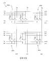
圖41和42示出了根據本發明另一實施例的記憶體格2150。格2150包括串聯連接的存取裝置2050A’和存儲裝置2050M,其中存取裝置2050A’和存儲裝置2050M是具有不同導電類型的電晶體;電阻改變元件2090串聯連接到記憶體件2050M。例如,記憶體件2050M是n型電晶體,存取器件2050A’是p型電晶體。如圖42所示,存取電晶體2042’包括第二導電類型的井區12’,例如n型,源區20’和第一導電類型的位線區22’,例如p型。第二導電類型的井區12’電連接到掩埋井區30,因此不浮動。例如在Widjaja-1中已經描述了諸如保持,讀取,寫入邏輯-1和寫入邏輯0操作的揮發性模式操作。41 and 42 illustrate a
當檢測到斷電時,例如,當用戶關閉電池2150的電源,或電源被無意中斷時,或者出於任何其他原因,電源至少暫時停止到電池2150,陰影操作可以是執行以將存儲在浮體區域24中的數據傳送到電阻改變記憶體2090。當電池恢復到電池2150時,存儲在非揮發性電阻改變記憶體2090上的電池2150的狀態恢復到浮體區域24,然後進行複位操作以將非揮發性電阻改變記憶體2090復位到初始狀態。When a power outage is detected, for example, when the user turns off power to the
圖43和44示出了根據本發明另一實施例的記憶體格2250。作為向BW端子76施加反偏壓的結果,在浮體區域24和掩埋層22的結中形成空乏區域23(圖44中以虛線包圍)。如果在源極線區域16或漏極區域18接地或負偏置的同時將正電壓施加到掩埋層22,則空乏區域23由於反向偏置的p-n結而延伸到浮體區域24中,並且頂部部分空乏區23位於絕緣層26的底部上方。因此,一個記憶體格2250的浮體區域24現在與相鄰記憶體格2250的浮體區域隔離,並形成用於過量電荷存儲的勢井。這已經在例如和美國專利9,029,922號,標題為“包含電浮體的記憶體件”(“Widjaja-6”)中上述內容一樣,它們完整引用於此,或者在根據本發明實施例的記憶體格1150,1250,1250F,1350,1450中。空乏區也可以由於向相鄰n井區施加反偏壓而形成。43 and 44 illustrate a
記憶體格2250還可包括具有不同導電類型的記憶體裝置2250M和存取裝置2250A。The
當向記憶體格2250施加電力時,電池2250處於揮發性模式操作並且像雙穩態浮體裝置那樣操作。例如在Widjaja-6中已經描述了諸如保持,讀取,寫入邏輯-1和寫入邏輯0操作的揮發性模式操作。When power is applied to the
當檢測到斷電時,例如,當用戶關閉電池2250的電源,或者電源被無意中斷時,或者出於任何其他原因,電源至少暫時停止到電池2250,陰影操作可以是執行以將存儲在浮體區域24中的數據傳送到電阻改變記憶體2090。當電池2250恢復供電時,存儲在非揮發性電阻改變記憶體2090上的電池2250的狀態恢復到浮體區域24,然後進行複位操作以將非揮發性電阻改變記憶體2090復位到初始狀態。When a power outage is detected, for example, when the user turns off power to the
圖45說明以三維鰭狀結構形成的記憶體格3350,其包括串聯的記憶體裝置3350M和存取裝置3350A,以及串聯連接到記憶體裝置3350M的電阻改變元件2090。記憶體格3350可以包括具有相同導電類型的記憶體設備3350M和訪問設備3350A,或者可以包括具有不同導電類型的記憶體設備3350M和訪問設備3350A。45 illustrates a
當功率施加到記憶體格3350時,格3350處於揮發性模式操作並且像雙穩態浮體裝置那樣操作。例如在Widjaja-1中已經描述了諸如保持,讀取,寫入邏輯-1和寫入邏輯0操作的揮發性模式操作。When power is applied to the
當檢測到斷電時,例如,當用戶關閉電池3350的電源,或者電源被無意中斷時,或者出於任何其他原因,電源至少暫時停止到電池3350,陰影操作可以是執行以傳送存儲在浮體區域24中的數據被傳送到電阻改變記憶體2090。當電池3350恢復供電時,存儲在非揮發性電阻改變記憶體2090上的電池3350的狀態恢復到浮體區24,然後進行複位操作以將非揮發性電阻改變記憶體2090復位到初始狀態。When a power outage is detected, for example, when the user turns off power to the
從前述內容可以看出,已經描述了具有電浮體的記憶體格。雖然前面對本發明的書面描述使普通技術人員能夠製作和使用目前被認為是其最佳模式的內容,但普通技術人員將理解並理解具體實施例的變化,組合和等同物的存在,方法和本文的實施例。因此,本發明不應受上述實施方案,方法和實施例的限制,而應受所要求保護的本發明範圍和精神內的所有實施方案和方法的限制。From the foregoing it can be seen that memory cells having electrically floating bodies have been described. While the foregoing written description of the invention enables one of ordinary skill to make and use what is presently believed to be its best mode, those of ordinary skill will appreciate and appreciate variations, combinations, and the like of the specific embodiments.Existence of peers, methods and examples herein. Accordingly, the present invention should not be limited by the embodiments, methods and examples described above, but by all embodiments and methods within the scope and spirit of the invention as claimed.
雖然已經參考本發明的特定實施例描述了本發明,但是本領域技術人員應該理解,在不脫離本發明的真實精神和範圍的情況下,可以進行各種改變並且可以替換等同物。另外,可以進行許多修改以使特定情況,材料,物質組成,過程,過程步驟或步驟適應本發明的目的,精神和範圍。所有這些修改都在所附權利要求的範圍內。While the invention has been described with reference to specific embodiments thereof, it will be understood by those skilled in the art that various changes may be made and equivalents may be substituted without departing from the true spirit and scope of the invention. In addition, many modifications may be made to adapt a particular situation, material, composition of matter, process, process step or steps to the objective, spirit and scope of the invention. All such modifications are within the scope of the appended claims.
12:襯底(圖2-6、13、18-26、29)、井區(圖30、31、34、36A、36B、38A-38C、40A、40B)12: Substrate (Fig. 2-6, 13, 18-26, 29), well area (Fig. 30, 31, 34, 36A, 36B, 38A-38C, 40A, 40B)
14:表面14: surface
16:源極線區域16: Source line area
18:漏極區域18: Drain area
20:井區域(圖18-26)、源區(圖30、31、34、36A、36B、38A-38C、40A、40B、43、44)20: Well area (Figure 18-26), source area (Figure 30, 31, 34, 36A, 36B, 38A-38C, 40A, 40B, 43, 44)
23:結中形成空乏區23: A depletion zone is formed in the junction
24:浮體區域24: Floating body area
26:絕緣層26: Insulation layer
60:閘極60: gate
62:閘極絕緣層62: Gate insulating layer
70:字線(WL)端子(圖2-6、18、19、21-26)、字線1(WL1)端子(圖29-45)70: word line (WL) terminal (Figure 2-6, 18, 19, 21-26), word line 1 (WL1) terminal (Figure 29-45)
72:源極線(SL)端子(圖2-6、18、19、21-26)、字線2(WL2)端子(圖29-45)72: Source line (SL) terminal (Figure 2-6, 18, 19, 21-26), word line 2 (WL2) terminal (Figure 29-45)
74:位線(BL)端子(圖2-6、18、19、21-26)、源極線(SL)端子(圖29-45)74: Bit line (BL) terminal (Figure 2-6, 18, 19, 21-26), source line (SL) terminal (Figure 29-45)
76:掩埋井(BW)端子(圖2-6、18、19、21-26)、位線(BL)端子(圖29-45)76: Buried well (BW) terminal (Figure 2-6, 18, 19, 21-26), bit line (BL) terminal (Figure 29-45)
78:襯底端子(圖2-6、18、19、21-26)、掩埋井(BW)端子(圖29-45)78: Substrate terminal (Figure 2-6, 18, 19, 21-26), buried well (BW) terminal (Figure 29-45)
1350:記憶體件1350: memory parts
Claims (14)
Translated fromChineseApplications Claiming Priority (6)
| Application Number | Priority Date | Filing Date | Title |
|---|---|---|---|
| US201862659628P | 2018-04-18 | 2018-04-18 | |
| US62/659,628 | 2018-04-18 | ||
| US201862661722P | 2018-04-24 | 2018-04-24 | |
| US62/661,722 | 2018-04-24 | ||
| US201862678975P | 2018-05-31 | 2018-05-31 | |
| US62/678,975 | 2018-05-31 |
Publications (2)
| Publication Number | Publication Date |
|---|---|
| TW202004756A TW202004756A (en) | 2020-01-16 |
| TWI787498Btrue TWI787498B (en) | 2022-12-21 |
Family
ID=68239063
Family Applications (5)
| Application Number | Title | Priority Date | Filing Date |
|---|---|---|---|
| TW108113471ATWI787498B (en) | 2018-04-18 | 2019-04-17 | A memory device comprising an electrically floating body transistor |
| TW113105941ATWI846663B (en) | 2018-04-18 | 2019-04-17 | A memory device comprising an electrically floating body transistor |
| TW113122070ATWI865411B (en) | 2018-04-18 | 2019-04-17 | A memory device comprising an electrically floating body transistor |
| TW112137853ATWI835705B (en) | 2018-04-18 | 2019-04-17 | A memory device comprising an electrically floating body transistor |
| TW111147140ATWI821065B (en) | 2018-04-18 | 2019-04-17 | A memory device comprising an electrically floating body transistor |
Family Applications After (4)
| Application Number | Title | Priority Date | Filing Date |
|---|---|---|---|
| TW113105941ATWI846663B (en) | 2018-04-18 | 2019-04-17 | A memory device comprising an electrically floating body transistor |
| TW113122070ATWI865411B (en) | 2018-04-18 | 2019-04-17 | A memory device comprising an electrically floating body transistor |
| TW112137853ATWI835705B (en) | 2018-04-18 | 2019-04-17 | A memory device comprising an electrically floating body transistor |
| TW111147140ATWI821065B (en) | 2018-04-18 | 2019-04-17 | A memory device comprising an electrically floating body transistor |
Country Status (3)
| Country | Link |
|---|---|
| US (2) | US11404419B2 (en) |
| TW (5) | TWI787498B (en) |
| WO (1) | WO2019204525A1 (en) |
Families Citing this family (7)
| Publication number | Priority date | Publication date | Assignee | Title |
|---|---|---|---|---|
| TWI787498B (en) | 2018-04-18 | 2022-12-21 | 美商季諾半導體股份有限公司 | A memory device comprising an electrically floating body transistor |
| US20240107741A1 (en)* | 2018-04-24 | 2024-03-28 | Zeno Semiconductor, Inc. | Memory Device Comprising an Electrically Floating Body Transistor |
| US11600663B2 (en) | 2019-01-11 | 2023-03-07 | Zeno Semiconductor, Inc. | Memory cell and memory array select transistor |
| US12439611B2 (en) | 2019-03-12 | 2025-10-07 | Zeno Semiconductor, Inc. | Memory cell and memory array select transistor |
| CN218004905U (en) | 2020-10-29 | 2022-12-09 | 意法半导体(克洛尔2)公司 | Electronic device and semiconductor structure |
| FR3115932A1 (en)* | 2020-10-29 | 2022-05-06 | Stmicroelectronics (Crolles 2) Sas | Phase change memory |
| FR3115931A1 (en) | 2020-10-29 | 2022-05-06 | Stmicroelectronics (Rousset) Sas | Phase change memory |
Citations (3)
| Publication number | Priority date | Publication date | Assignee | Title |
|---|---|---|---|---|
| US20100046287A1 (en)* | 2008-08-22 | 2010-02-25 | Yuniarto Widjaja | Semiconductor memory having both volatile and non-volatile functionality including resistance change material and method of operating |
| US20140252451A1 (en)* | 2013-03-09 | 2014-09-11 | Jin-Woo Han | Memory device comprising electrically floating body transistor |
| US20150023105A1 (en)* | 2012-02-16 | 2015-01-22 | Zeno Semiconductor, Inc. | Memory Cell Comprising First and Second Transistors and Methods of Operating |
Family Cites Families (120)
| Publication number | Priority date | Publication date | Assignee | Title |
|---|---|---|---|---|
| US4274012A (en) | 1979-01-24 | 1981-06-16 | Xicor, Inc. | Substrate coupled floating gate memory cell |
| JP2685770B2 (en) | 1987-12-28 | 1997-12-03 | 株式会社東芝 | Nonvolatile semiconductor memory device |
| US5844842A (en) | 1989-02-06 | 1998-12-01 | Hitachi, Ltd. | Nonvolatile semiconductor memory device |
| US4975764A (en) | 1989-06-22 | 1990-12-04 | David Sarnoff Research Center, Inc. | High density BiCMOS circuits and methods of making same |
| JP2660056B2 (en) | 1989-09-12 | 1997-10-08 | 三菱電機株式会社 | Complementary MOS semiconductor device |
| GB2256735B (en) | 1991-06-12 | 1995-06-21 | Intel Corp | Non-volatile disk cache |
| US5465249A (en) | 1991-11-26 | 1995-11-07 | Cree Research, Inc. | Nonvolatile random access memory device having transistor and capacitor made in silicon carbide substrate |
| US5365477A (en) | 1992-06-16 | 1994-11-15 | The United States Of America As Represented By The Secretary Of The Navy | Dynamic random access memory device |
| KR100473308B1 (en) | 1995-01-31 | 2005-03-14 | 가부시끼가이샤 히다치 세이사꾸쇼 | Nonvolatile memory device |
| US6163048A (en) | 1995-10-25 | 2000-12-19 | Cypress Semiconductor Corporation | Semiconductor non-volatile memory device having a NAND cell structure |
| US5581504A (en) | 1995-11-14 | 1996-12-03 | Programmable Microelectronics Corp. | Non-volatile electrically erasable memory with PMOS transistor NAND gate structure |
| US5767549A (en) | 1996-07-03 | 1998-06-16 | International Business Machines Corporation | SOI CMOS structure |
| US5896315A (en) | 1997-04-11 | 1999-04-20 | Programmable Silicon Solutions | Nonvolatile memory |
| US6835979B1 (en) | 1997-04-11 | 2004-12-28 | Altera Corporation | Nonvolatle memory |
| JP3951443B2 (en) | 1997-09-02 | 2007-08-01 | ソニー株式会社 | Nonvolatile semiconductor memory device and writing method thereof |
| JP3492168B2 (en) | 1997-10-21 | 2004-02-03 | シャープ株式会社 | Nonvolatile semiconductor memory device |
| US6005818A (en) | 1998-01-20 | 1999-12-21 | Stmicroelectronics, Inc. | Dynamic random access memory device with a latching mechanism that permits hidden refresh operations |
| AU3073800A (en) | 1999-02-01 | 2000-08-25 | Hitachi Limited | Semiconductor integrated circuit and nonvolatile memory element |
| US6356485B1 (en) | 1999-02-13 | 2002-03-12 | Integrated Device Technology, Inc. | Merging write cycles by comparing at least a portion of the respective write cycle addresses |
| US6141248A (en) | 1999-07-29 | 2000-10-31 | Micron Technology, Inc. | DRAM and SRAM memory cells with repressed memory |
| KR100323140B1 (en) | 2000-01-17 | 2002-02-06 | 윤종용 | NAND-type flash memory device and method of fabricating the same |
| DE10012105B4 (en) | 2000-03-13 | 2007-08-23 | Infineon Technologies Ag | Method for reading non-volatile semiconductor memory devices |
| JP2001274265A (en) | 2000-03-28 | 2001-10-05 | Mitsubishi Electric Corp | Semiconductor device |
| JP2001358313A (en) | 2000-06-14 | 2001-12-26 | Hitachi Ltd | Semiconductor device |
| KR100821456B1 (en) | 2000-08-14 | 2008-04-11 | 샌디스크 쓰리디 엘엘씨 | Dense array and charge storage device and manufacturing method thereof |
| KR20030041974A (en) | 2000-08-24 | 2003-05-27 | 코바 테크놀로지스, 인크. | Single transistor rare earth manganite ferroelectric nonvolatile memory cell |
| JP2002133878A (en) | 2000-10-23 | 2002-05-10 | Hitachi Ltd | Nonvolatile memory circuit and semiconductor integrated circuit |
| EP1384232A4 (en) | 2001-04-05 | 2008-11-19 | T Ram Inc | Dynamic data restore in thyristor-based memory device |
| US6433391B1 (en) | 2001-06-08 | 2002-08-13 | Advanced Micro Devices, Inc. | Bonded SOI for floating body and metal gettering control |
| TWI230392B (en) | 2001-06-18 | 2005-04-01 | Innovative Silicon Sa | Semiconductor device |
| US6686624B2 (en) | 2002-03-11 | 2004-02-03 | Monolithic System Technology, Inc. | Vertical one-transistor floating-body DRAM cell in bulk CMOS process with electrically isolated charge storage region |
| US6661042B2 (en) | 2002-03-11 | 2003-12-09 | Monolithic System Technology, Inc. | One-transistor floating-body DRAM cell in bulk CMOS process with electrically isolated charge storage region |
| US6954377B2 (en) | 2002-03-19 | 2005-10-11 | O2Ic, Inc. | Non-volatile differential dynamic random access memory |
| EP1355316B1 (en) | 2002-04-18 | 2007-02-21 | Innovative Silicon SA | Data storage device and refreshing method for use with such device |
| US7042052B2 (en) | 2003-02-10 | 2006-05-09 | Micron Technology, Inc. | Transistor constructions and electronic devices |
| US6956256B2 (en) | 2003-03-04 | 2005-10-18 | Micron Technology Inc. | Vertical gain cell |
| US20040228168A1 (en) | 2003-05-13 | 2004-11-18 | Richard Ferrant | Semiconductor memory device and method of operating same |
| US7227803B2 (en) | 2003-07-31 | 2007-06-05 | Brocade Communications Systems, Inc. | Apparatus for reducing data corruption in a non-volatile memory |
| DE10350751B4 (en) | 2003-10-30 | 2008-04-24 | Infineon Technologies Ag | Method for producing a vertical field effect transistor and field effect memory transistor, in particular FLASH memory transistor |
| US6969656B2 (en) | 2003-12-05 | 2005-11-29 | Freescale Semiconductor, Inc. | Method and circuit for multiplying signals with a transistor having more than one independent gate structure |
| JP2005243709A (en) | 2004-02-24 | 2005-09-08 | Toshiba Corp | Semiconductor device and manufacturing method thereof |
| JP4331053B2 (en) | 2004-05-27 | 2009-09-16 | 株式会社東芝 | Semiconductor memory device |
| KR100621628B1 (en) | 2004-05-31 | 2006-09-19 | 삼성전자주식회사 | Nonvolatile Memory Cells and Their Formation Methods |
| US7009887B1 (en) | 2004-06-03 | 2006-03-07 | Fasl Llc | Method of determining voltage compensation for flash memory devices |
| US7118986B2 (en) | 2004-06-16 | 2006-10-10 | International Business Machines Corporation | STI formation in semiconductor device including SOI and bulk silicon regions |
| US7259420B2 (en) | 2004-07-28 | 2007-08-21 | International Business Machines Corporation | Multiple-gate device with floating back gate |
| US7145186B2 (en) | 2004-08-24 | 2006-12-05 | Micron Technology, Inc. | Memory cell with trenched gated thyristor |
| KR100591770B1 (en) | 2004-09-01 | 2006-06-26 | 삼성전자주식회사 | Flash memory device using semiconductor pin and manufacturing method thereof |
| KR100598109B1 (en) | 2004-10-08 | 2006-07-07 | 삼성전자주식회사 | Nonvolatile Memory Device and Formation Method |
| US7301803B2 (en) | 2004-12-22 | 2007-11-27 | Innovative Silicon S.A. | Bipolar reading technique for a memory cell having an electrically floating body transistor |
| US7307268B2 (en) | 2005-01-19 | 2007-12-11 | Sandisk Corporation | Structure and method for biasing phase change memory array for reliable writing |
| US7504302B2 (en) | 2005-03-18 | 2009-03-17 | Freescale Semiconductor, Inc. | Process of forming a non-volatile memory cell including a capacitor structure |
| US7602006B2 (en) | 2005-04-20 | 2009-10-13 | Taiwan Semiconductor Manufacturing Co., Ltd. | Semiconductor flash device |
| US7376006B2 (en) | 2005-05-13 | 2008-05-20 | International Business Machines Corporation | Enhanced programming performance in a nonvolatile memory device having a bipolar programmable storage element |
| US7208795B2 (en) | 2005-05-24 | 2007-04-24 | Atmel Corporation | Low-cost, low-voltage single-layer polycrystalline EEPROM memory cell integration into BiCMOS technology |
| US7205601B2 (en) | 2005-06-09 | 2007-04-17 | Taiwan Semiconductor Manufacturing Company, Ltd. | FinFET split gate EEPROM structure and method of its fabrication |
| CN1897282A (en) | 2005-06-30 | 2007-01-17 | St微电子克鲁勒斯图股份公司 | Memory cell with an isolated-body mos transistor with reinforced memory effect |
| US20070013007A1 (en)* | 2005-07-15 | 2007-01-18 | Kabushiki Kaisha Toshiba | Semiconductor device and method of fabricating the same |
| FR2889356A1 (en)* | 2005-07-26 | 2007-02-02 | St Microelectronics Crolles 2 | MEMORY CELL HAS AN INSULATED BODY TRANSISTOR WITH ENHANCED READING SENSITIVITY |
| TWI263310B (en) | 2005-09-28 | 2006-10-01 | Powerchip Semiconductor Corp | Non-volatile memory and fabricating method thereof |
| KR100663366B1 (en) | 2005-10-26 | 2007-01-02 | 삼성전자주식회사 | Flash memory device manufacturing method having self-aligned floating gate and related devices |
| WO2007070808A2 (en) | 2005-12-12 | 2007-06-21 | The Regents Of The University Of California | Multi-bit-per-cell nvm structures and architecture |
| JP2007194259A (en) | 2006-01-17 | 2007-08-02 | Toshiba Corp | Semiconductor device and manufacturing method thereof |
| US7542345B2 (en) | 2006-02-16 | 2009-06-02 | Innovative Silicon Isi Sa | Multi-bit memory cell having electrically floating body transistor, and method of programming and reading same |
| US7535060B2 (en) | 2006-03-08 | 2009-05-19 | Freescale Semiconductor, Inc. | Charge storage structure formation in transistor with vertical channel region |
| US7439594B2 (en) | 2006-03-16 | 2008-10-21 | Micron Technology, Inc. | Stacked non-volatile memory with silicon carbide-based amorphous silicon thin film transistors |
| EP1835530A3 (en) | 2006-03-17 | 2009-01-28 | Samsung Electronics Co., Ltd. | Non-volatile memory device and method of manufacturing the same |
| KR100810614B1 (en) | 2006-08-23 | 2008-03-06 | 삼성전자주식회사 | Semiconductor memory device having DRAM cell mode and nonvolatile memory cell mode and method of operating same |
| JP4364227B2 (en) | 2006-09-29 | 2009-11-11 | 株式会社東芝 | Semiconductor memory device |
| US8325530B2 (en) | 2006-10-03 | 2012-12-04 | Macronix International Co., Ltd. | Cell operation methods using gate-injection for floating gate NAND flash memory |
| US8077536B2 (en) | 2008-08-05 | 2011-12-13 | Zeno Semiconductor, Inc. | Method of operating semiconductor memory device with floating body transistor using silicon controlled rectifier principle |
| US9391079B2 (en) | 2007-11-29 | 2016-07-12 | Zeno Semiconductor, Inc. | Compact semiconductor memory device having reduced number of contacts, methods of operating and methods of making |
| US9601493B2 (en) | 2006-11-29 | 2017-03-21 | Zeno Semiconductor, Inc | Compact semiconductor memory device having reduced number of contacts, methods of operating and methods of making |
| US8194451B2 (en) | 2007-11-29 | 2012-06-05 | Zeno Semiconductor, Inc. | Memory cells, memory cell arrays, methods of using and methods of making |
| US8514622B2 (en) | 2007-11-29 | 2013-08-20 | Zeno Semiconductor, Inc. | Compact semiconductor memory device having reduced number of contacts, methods of operating and methods of making |
| US8547756B2 (en) | 2010-10-04 | 2013-10-01 | Zeno Semiconductor, Inc. | Semiconductor memory device having an electrically floating body transistor |
| US7760548B2 (en) | 2006-11-29 | 2010-07-20 | Yuniarto Widjaja | Semiconductor memory having both volatile and non-volatile functionality and method of operating |
| US7450423B2 (en) | 2007-01-03 | 2008-11-11 | Macronix International Co., Ltd. | Methods of operating non-volatile memory cells having an oxide/nitride multilayer insulating structure |
| US7447068B2 (en) | 2007-03-19 | 2008-11-04 | Macronix International Co., Ltd. | Method for programming a multilevel memory |
| US7452776B1 (en) | 2007-04-24 | 2008-11-18 | Promos Technoloies Pte. Ltd. | Integrated circuits with substrate protrusions, including (but not limited to) floating gate memories |
| JP2009037703A (en) | 2007-08-02 | 2009-02-19 | Toshiba Corp | Resistance change memory |
| US7674669B2 (en) | 2007-09-07 | 2010-03-09 | Micron Technology, Inc. | FIN field effect transistor |
| TWI351767B (en) | 2007-10-02 | 2011-11-01 | Nanya Technology Corp | Two-bit flash memory |
| US7759715B2 (en) | 2007-10-15 | 2010-07-20 | Micron Technology, Inc. | Memory cell comprising dynamic random access memory (DRAM) nanoparticles and nonvolatile memory (NVM) nanoparticle |
| US8059459B2 (en) | 2007-10-24 | 2011-11-15 | Zeno Semiconductor, Inc. | Semiconductor memory having both volatile and non-volatile functionality and method of operating |
| US20090108351A1 (en) | 2007-10-26 | 2009-04-30 | International Business Machines Corporation | Finfet memory device with dual separate gates and method of operation |
| KR100930074B1 (en)* | 2007-11-20 | 2009-12-08 | 경북대학교 산학협력단 | Single Transistor Floating Body DRAM Cell Device with Nonvolatile Functions |
| US8130547B2 (en) | 2007-11-29 | 2012-03-06 | Zeno Semiconductor, Inc. | Method of maintaining the state of semiconductor memory having electrically floating body transistor |
| US8264875B2 (en)* | 2010-10-04 | 2012-09-11 | Zeno Semiconducor, Inc. | Semiconductor memory device having an electrically floating body transistor |
| US8174886B2 (en) | 2007-11-29 | 2012-05-08 | Zeno Semiconductor, Inc. | Semiconductor memory having electrically floating body transistor |
| US8130548B2 (en) | 2007-11-29 | 2012-03-06 | Zeno Semiconductor, Inc. | Semiconductor memory having electrically floating body transistor |
| US10403361B2 (en) | 2007-11-29 | 2019-09-03 | Zeno Semiconductor, Inc. | Memory cells, memory cell arrays, methods of using and methods of making |
| US8331150B2 (en) | 2008-01-03 | 2012-12-11 | Aplus Flash Technology, Inc. | Integrated SRAM and FLOTOX EEPROM memory device |
| US8014200B2 (en) | 2008-04-08 | 2011-09-06 | Zeno Semiconductor, Inc. | Semiconductor memory having volatile and multi-bit, non-volatile functionality and methods of operating |
| US7701763B2 (en) | 2008-04-23 | 2010-04-20 | Micron Technology, Inc. | Leakage compensation during program and read operations |
| KR101498873B1 (en) | 2008-07-08 | 2015-03-04 | 삼성전자주식회사 | Method for operating an memory device having characters of DRAM and Non-volatile memory |
| US7933140B2 (en) | 2008-10-02 | 2011-04-26 | Micron Technology, Inc. | Techniques for reducing a voltage swing |
| US7924630B2 (en) | 2008-10-15 | 2011-04-12 | Micron Technology, Inc. | Techniques for simultaneously driving a plurality of source lines |
| KR101442177B1 (en)* | 2008-12-18 | 2014-09-18 | 삼성전자주식회사 | Processes for fabricating semiconductor devices with capacitorless one-transistor memory cells |
| US11908899B2 (en)* | 2009-02-20 | 2024-02-20 | Zeno Semiconductor, Inc. | MOSFET and memory cell having improved drain current through back bias application |
| WO2016176248A1 (en) | 2015-04-29 | 2016-11-03 | Zeno Semiconductor, Inc. | A mosfet and memory cell having improved drain current through back bias application |
| IN2012DN06399A (en) | 2010-02-07 | 2015-10-02 | Zeno Semiconductor Inc | |
| US10461084B2 (en) | 2010-03-02 | 2019-10-29 | Zeno Semiconductor, Inc. | Compact semiconductor memory device having reduced number of contacts, methods of operating and methods of making |
| US10340276B2 (en) | 2010-03-02 | 2019-07-02 | Zeno Semiconductor, Inc. | Method of maintaining the state of semiconductor memory having electrically floating body transistor |
| US9922981B2 (en) | 2010-03-02 | 2018-03-20 | Zeno Semiconductor, Inc. | Compact semiconductor memory device having reduced number of contacts, methods of operating and methods of making |
| US8582359B2 (en) | 2010-11-16 | 2013-11-12 | Zeno Semiconductor, Inc. | Dual-port semiconductor memory and first-in first-out (FIFO) memory having electrically floating body transistor |
| US8957458B2 (en) | 2011-03-24 | 2015-02-17 | Zeno Semiconductor, Inc. | Asymmetric semiconductor memory device having electrically floating body transistor |
| US9025358B2 (en) | 2011-10-13 | 2015-05-05 | Zeno Semiconductor Inc | Semiconductor memory having both volatile and non-volatile functionality comprising resistive change material and method of operating |
| CN107331416B (en) | 2012-02-16 | 2020-11-10 | 芝诺半导体有限公司 | Memory cell including primary and secondary transistors |
| FR2990553B1 (en)* | 2012-05-09 | 2015-02-20 | Soitec Silicon On Insulator | COMPLEMENTARY FET INJECTION FOR FLOATING BODY CELL |
| US9208880B2 (en) | 2013-01-14 | 2015-12-08 | Zeno Semiconductor, Inc. | Content addressable memory device having electrically floating body transistor |
| US9275723B2 (en) | 2013-04-10 | 2016-03-01 | Zeno Semiconductor, Inc. | Scalable floating body memory cell for memory compilers and method of using floating body memories with memory compilers |
| US9368625B2 (en) | 2013-05-01 | 2016-06-14 | Zeno Semiconductor, Inc. | NAND string utilizing floating body memory cell |
| US9281022B2 (en) | 2013-07-10 | 2016-03-08 | Zeno Semiconductor, Inc. | Systems and methods for reducing standby power in floating body memory devices |
| US9548119B2 (en) | 2014-01-15 | 2017-01-17 | Zeno Semiconductor, Inc | Memory device comprising an electrically floating body transistor |
| US9496053B2 (en) | 2014-08-15 | 2016-11-15 | Zeno Semiconductor, Inc. | Memory device comprising electrically floating body transistor |
| US10553683B2 (en) | 2015-04-29 | 2020-02-04 | Zeno Semiconductor, Inc. | MOSFET and memory cell having improved drain current through back bias application |
| US10079301B2 (en) | 2016-11-01 | 2018-09-18 | Zeno Semiconductor, Inc. | Memory device comprising an electrically floating body transistor and methods of using |
| TWI787498B (en)* | 2018-04-18 | 2022-12-21 | 美商季諾半導體股份有限公司 | A memory device comprising an electrically floating body transistor |
| US11600663B2 (en) | 2019-01-11 | 2023-03-07 | Zeno Semiconductor, Inc. | Memory cell and memory array select transistor |
- 2019
- 2019-04-17TWTW108113471Apatent/TWI787498B/enactive
- 2019-04-17WOPCT/US2019/027994patent/WO2019204525A1/ennot_activeCeased
- 2019-04-17TWTW113105941Apatent/TWI846663B/enactive
- 2019-04-17USUS17/047,623patent/US11404419B2/enactiveActive
- 2019-04-17TWTW113122070Apatent/TWI865411B/enactive
- 2019-04-17TWTW112137853Apatent/TWI835705B/enactive
- 2019-04-17TWTW111147140Apatent/TWI821065B/enactive
- 2022
- 2022-07-13USUS17/863,848patent/US11882684B2/enactiveActive
Patent Citations (4)
| Publication number | Priority date | Publication date | Assignee | Title |
|---|---|---|---|---|
| US20100046287A1 (en)* | 2008-08-22 | 2010-02-25 | Yuniarto Widjaja | Semiconductor memory having both volatile and non-volatile functionality including resistance change material and method of operating |
| US20150023105A1 (en)* | 2012-02-16 | 2015-01-22 | Zeno Semiconductor, Inc. | Memory Cell Comprising First and Second Transistors and Methods of Operating |
| US20140252451A1 (en)* | 2013-03-09 | 2014-09-11 | Jin-Woo Han | Memory device comprising electrically floating body transistor |
| US9831247B2 (en)* | 2013-03-09 | 2017-11-28 | Zeno Semiconductor Inc. | Memory device comprising electrically floating body transistor |
Also Published As
| Publication number | Publication date |
|---|---|
| TWI865411B (en) | 2024-12-01 |
| WO2019204525A1 (en) | 2019-10-24 |
| US20220344337A1 (en) | 2022-10-27 |
| US11404419B2 (en) | 2022-08-02 |
| TW202403748A (en) | 2024-01-16 |
| TWI835705B (en) | 2024-03-11 |
| TWI846663B (en) | 2024-06-21 |
| TW202314706A (en) | 2023-04-01 |
| TW202445575A (en) | 2024-11-16 |
| TW202424971A (en) | 2024-06-16 |
| TWI821065B (en) | 2023-11-01 |
| US11882684B2 (en) | 2024-01-23 |
| US20210159227A1 (en) | 2021-05-27 |
| TW202004756A (en) | 2020-01-16 |
Similar Documents
| Publication | Publication Date | Title |
|---|---|---|
| US20250061945A1 (en) | Semiconductor Memory Having Both Volatile and Non-Volatile Functionality Comprising Resistive Change Material and Method of Operating | |
| US11348922B2 (en) | Memory cell comprising first and second transistors and methods of operating | |
| TWI787498B (en) | A memory device comprising an electrically floating body transistor | |
| US20250037766A1 (en) | Semiconductor Memory Having Both Volatile and Non-Volatile Functionality Including Resistance Change Material and Method of Operating | |
| US10991697B2 (en) | NAND string utilizing floating body memory cell | |
| US20220278104A1 (en) | Memory Cell Comprising First and Second Transistors and Methods of Operating | |
| US20240107741A1 (en) | Memory Device Comprising an Electrically Floating Body Transistor | |
| US20240243492A1 (en) | Memory Cell Comprising First and Second Transistors and Methods of Operating |