TWI784135B - Method, system, and non-transitory computer readable medium for producing image on substrate - Google Patents
Method, system, and non-transitory computer readable medium for producing image on substrateDownload PDFInfo
- Publication number
- TWI784135B TWI784135BTW108105386ATW108105386ATWI784135BTW I784135 BTWI784135 BTW I784135BTW 108105386 ATW108105386 ATW 108105386ATW 108105386 ATW108105386 ATW 108105386ATW I784135 BTWI784135 BTW I784135B
- Authority
- TW
- Taiwan
- Prior art keywords
- emitter
- substrate
- emitters
- arrays
- instructions
- Prior art date
Links
Images


Classifications
- G—PHYSICS
- G03—PHOTOGRAPHY; CINEMATOGRAPHY; ANALOGOUS TECHNIQUES USING WAVES OTHER THAN OPTICAL WAVES; ELECTROGRAPHY; HOLOGRAPHY
- G03F—PHOTOMECHANICAL PRODUCTION OF TEXTURED OR PATTERNED SURFACES, e.g. FOR PRINTING, FOR PROCESSING OF SEMICONDUCTOR DEVICES; MATERIALS THEREFOR; ORIGINALS THEREFOR; APPARATUS SPECIALLY ADAPTED THEREFOR
- G03F1/00—Originals for photomechanical production of textured or patterned surfaces, e.g., masks, photo-masks, reticles; Mask blanks or pellicles therefor; Containers specially adapted therefor; Preparation thereof
- G03F1/68—Preparation processes not covered by groups G03F1/20 - G03F1/50
- G03F1/76—Patterning of masks by imaging
- G—PHYSICS
- G03—PHOTOGRAPHY; CINEMATOGRAPHY; ANALOGOUS TECHNIQUES USING WAVES OTHER THAN OPTICAL WAVES; ELECTROGRAPHY; HOLOGRAPHY
- G03F—PHOTOMECHANICAL PRODUCTION OF TEXTURED OR PATTERNED SURFACES, e.g. FOR PRINTING, FOR PROCESSING OF SEMICONDUCTOR DEVICES; MATERIALS THEREFOR; ORIGINALS THEREFOR; APPARATUS SPECIALLY ADAPTED THEREFOR
- G03F7/00—Photomechanical, e.g. photolithographic, production of textured or patterned surfaces, e.g. printing surfaces; Materials therefor, e.g. comprising photoresists; Apparatus specially adapted therefor
- G03F7/70—Microphotolithographic exposure; Apparatus therefor
- G03F7/70383—Direct write, i.e. pattern is written directly without the use of a mask by one or multiple beams
- G03F7/70391—Addressable array sources specially adapted to produce patterns, e.g. addressable LED arrays
- G—PHYSICS
- G03—PHOTOGRAPHY; CINEMATOGRAPHY; ANALOGOUS TECHNIQUES USING WAVES OTHER THAN OPTICAL WAVES; ELECTROGRAPHY; HOLOGRAPHY
- G03F—PHOTOMECHANICAL PRODUCTION OF TEXTURED OR PATTERNED SURFACES, e.g. FOR PRINTING, FOR PROCESSING OF SEMICONDUCTOR DEVICES; MATERIALS THEREFOR; ORIGINALS THEREFOR; APPARATUS SPECIALLY ADAPTED THEREFOR
- G03F7/00—Photomechanical, e.g. photolithographic, production of textured or patterned surfaces, e.g. printing surfaces; Materials therefor, e.g. comprising photoresists; Apparatus specially adapted therefor
- G03F7/0005—Production of optical devices or components in so far as characterised by the lithographic processes or materials used therefor
- G03F7/0007—Filters, e.g. additive colour filters; Components for display devices
- G—PHYSICS
- G03—PHOTOGRAPHY; CINEMATOGRAPHY; ANALOGOUS TECHNIQUES USING WAVES OTHER THAN OPTICAL WAVES; ELECTROGRAPHY; HOLOGRAPHY
- G03F—PHOTOMECHANICAL PRODUCTION OF TEXTURED OR PATTERNED SURFACES, e.g. FOR PRINTING, FOR PROCESSING OF SEMICONDUCTOR DEVICES; MATERIALS THEREFOR; ORIGINALS THEREFOR; APPARATUS SPECIALLY ADAPTED THEREFOR
- G03F7/00—Photomechanical, e.g. photolithographic, production of textured or patterned surfaces, e.g. printing surfaces; Materials therefor, e.g. comprising photoresists; Apparatus specially adapted therefor
- G03F7/70—Microphotolithographic exposure; Apparatus therefor
- G03F7/70008—Production of exposure light, i.e. light sources
- G03F7/70041—Production of exposure light, i.e. light sources by pulsed sources, e.g. multiplexing, pulse duration, interval control or intensity control
- G—PHYSICS
- G03—PHOTOGRAPHY; CINEMATOGRAPHY; ANALOGOUS TECHNIQUES USING WAVES OTHER THAN OPTICAL WAVES; ELECTROGRAPHY; HOLOGRAPHY
- G03F—PHOTOMECHANICAL PRODUCTION OF TEXTURED OR PATTERNED SURFACES, e.g. FOR PRINTING, FOR PROCESSING OF SEMICONDUCTOR DEVICES; MATERIALS THEREFOR; ORIGINALS THEREFOR; APPARATUS SPECIALLY ADAPTED THEREFOR
- G03F7/00—Photomechanical, e.g. photolithographic, production of textured or patterned surfaces, e.g. printing surfaces; Materials therefor, e.g. comprising photoresists; Apparatus specially adapted therefor
- G03F7/70—Microphotolithographic exposure; Apparatus therefor
- G03F7/70216—Mask projection systems
- G03F7/70358—Scanning exposure, i.e. relative movement of patterned beam and workpiece during imaging
- G—PHYSICS
- G03—PHOTOGRAPHY; CINEMATOGRAPHY; ANALOGOUS TECHNIQUES USING WAVES OTHER THAN OPTICAL WAVES; ELECTROGRAPHY; HOLOGRAPHY
- G03F—PHOTOMECHANICAL PRODUCTION OF TEXTURED OR PATTERNED SURFACES, e.g. FOR PRINTING, FOR PROCESSING OF SEMICONDUCTOR DEVICES; MATERIALS THEREFOR; ORIGINALS THEREFOR; APPARATUS SPECIALLY ADAPTED THEREFOR
- G03F7/00—Photomechanical, e.g. photolithographic, production of textured or patterned surfaces, e.g. printing surfaces; Materials therefor, e.g. comprising photoresists; Apparatus specially adapted therefor
- G03F7/70—Microphotolithographic exposure; Apparatus therefor
- G03F7/70383—Direct write, i.e. pattern is written directly without the use of a mask by one or multiple beams
- G03F7/704—Scanned exposure beam, e.g. raster-, rotary- and vector scanning
- G—PHYSICS
- G03—PHOTOGRAPHY; CINEMATOGRAPHY; ANALOGOUS TECHNIQUES USING WAVES OTHER THAN OPTICAL WAVES; ELECTROGRAPHY; HOLOGRAPHY
- G03F—PHOTOMECHANICAL PRODUCTION OF TEXTURED OR PATTERNED SURFACES, e.g. FOR PRINTING, FOR PROCESSING OF SEMICONDUCTOR DEVICES; MATERIALS THEREFOR; ORIGINALS THEREFOR; APPARATUS SPECIALLY ADAPTED THEREFOR
- G03F7/00—Photomechanical, e.g. photolithographic, production of textured or patterned surfaces, e.g. printing surfaces; Materials therefor, e.g. comprising photoresists; Apparatus specially adapted therefor
- G03F7/70—Microphotolithographic exposure; Apparatus therefor
- G03F7/70408—Interferometric lithography; Holographic lithography; Self-imaging lithography, e.g. utilizing the Talbot effect
- G—PHYSICS
- G03—PHOTOGRAPHY; CINEMATOGRAPHY; ANALOGOUS TECHNIQUES USING WAVES OTHER THAN OPTICAL WAVES; ELECTROGRAPHY; HOLOGRAPHY
- G03F—PHOTOMECHANICAL PRODUCTION OF TEXTURED OR PATTERNED SURFACES, e.g. FOR PRINTING, FOR PROCESSING OF SEMICONDUCTOR DEVICES; MATERIALS THEREFOR; ORIGINALS THEREFOR; APPARATUS SPECIALLY ADAPTED THEREFOR
- G03F7/00—Photomechanical, e.g. photolithographic, production of textured or patterned surfaces, e.g. printing surfaces; Materials therefor, e.g. comprising photoresists; Apparatus specially adapted therefor
- G03F7/70—Microphotolithographic exposure; Apparatus therefor
- G03F7/70425—Imaging strategies, e.g. for increasing throughput or resolution, printing product fields larger than the image field or compensating lithography- or non-lithography errors, e.g. proximity correction, mix-and-match, stitching or double patterning
- G03F7/70475—Stitching, i.e. connecting image fields to produce a device field, the field occupied by a device such as a memory chip, processor chip, CCD, flat panel display
- G—PHYSICS
- G03—PHOTOGRAPHY; CINEMATOGRAPHY; ANALOGOUS TECHNIQUES USING WAVES OTHER THAN OPTICAL WAVES; ELECTROGRAPHY; HOLOGRAPHY
- G03F—PHOTOMECHANICAL PRODUCTION OF TEXTURED OR PATTERNED SURFACES, e.g. FOR PRINTING, FOR PROCESSING OF SEMICONDUCTOR DEVICES; MATERIALS THEREFOR; ORIGINALS THEREFOR; APPARATUS SPECIALLY ADAPTED THEREFOR
- G03F7/00—Photomechanical, e.g. photolithographic, production of textured or patterned surfaces, e.g. printing surfaces; Materials therefor, e.g. comprising photoresists; Apparatus specially adapted therefor
- G03F7/70—Microphotolithographic exposure; Apparatus therefor
- G03F7/70483—Information management; Active and passive control; Testing; Wafer monitoring, e.g. pattern monitoring
- G03F7/7055—Exposure light control in all parts of the microlithographic apparatus, e.g. pulse length control or light interruption
- G03F7/70558—Dose control, i.e. achievement of a desired dose
- G—PHYSICS
- G03—PHOTOGRAPHY; CINEMATOGRAPHY; ANALOGOUS TECHNIQUES USING WAVES OTHER THAN OPTICAL WAVES; ELECTROGRAPHY; HOLOGRAPHY
- G03F—PHOTOMECHANICAL PRODUCTION OF TEXTURED OR PATTERNED SURFACES, e.g. FOR PRINTING, FOR PROCESSING OF SEMICONDUCTOR DEVICES; MATERIALS THEREFOR; ORIGINALS THEREFOR; APPARATUS SPECIALLY ADAPTED THEREFOR
- G03F7/00—Photomechanical, e.g. photolithographic, production of textured or patterned surfaces, e.g. printing surfaces; Materials therefor, e.g. comprising photoresists; Apparatus specially adapted therefor
- G03F7/70—Microphotolithographic exposure; Apparatus therefor
- G03F7/70483—Information management; Active and passive control; Testing; Wafer monitoring, e.g. pattern monitoring
- G03F7/70605—Workpiece metrology
- G03F7/70616—Monitoring the printed patterns
- H—ELECTRICITY
- H01—ELECTRIC ELEMENTS
- H01L—SEMICONDUCTOR DEVICES NOT COVERED BY CLASS H10
- H01L21/00—Processes or apparatus adapted for the manufacture or treatment of semiconductor or solid state devices or of parts thereof
- H01L21/02—Manufacture or treatment of semiconductor devices or of parts thereof
- H01L21/027—Making masks on semiconductor bodies for further photolithographic processing not provided for in group H01L21/18 or H01L21/34
- H—ELECTRICITY
- H01—ELECTRIC ELEMENTS
- H01S—DEVICES USING THE PROCESS OF LIGHT AMPLIFICATION BY STIMULATED EMISSION OF RADIATION [LASER] TO AMPLIFY OR GENERATE LIGHT; DEVICES USING STIMULATED EMISSION OF ELECTROMAGNETIC RADIATION IN WAVE RANGES OTHER THAN OPTICAL
- H01S5/00—Semiconductor lasers
- H01S5/02—Structural details or components not essential to laser action
- H01S5/026—Monolithically integrated components, e.g. waveguides, monitoring photo-detectors, drivers
- H—ELECTRICITY
- H01—ELECTRIC ELEMENTS
- H01S—DEVICES USING THE PROCESS OF LIGHT AMPLIFICATION BY STIMULATED EMISSION OF RADIATION [LASER] TO AMPLIFY OR GENERATE LIGHT; DEVICES USING STIMULATED EMISSION OF ELECTROMAGNETIC RADIATION IN WAVE RANGES OTHER THAN OPTICAL
- H01S5/00—Semiconductor lasers
- H01S5/30—Structure or shape of the active region; Materials used for the active region
- H01S5/3013—AIIIBV compounds
- H—ELECTRICITY
- H01—ELECTRIC ELEMENTS
- H01S—DEVICES USING THE PROCESS OF LIGHT AMPLIFICATION BY STIMULATED EMISSION OF RADIATION [LASER] TO AMPLIFY OR GENERATE LIGHT; DEVICES USING STIMULATED EMISSION OF ELECTROMAGNETIC RADIATION IN WAVE RANGES OTHER THAN OPTICAL
- H01S5/00—Semiconductor lasers
- H01S5/40—Arrangement of two or more semiconductor lasers, not provided for in groups H01S5/02 - H01S5/30
- H01S5/4025—Array arrangements, e.g. constituted by discrete laser diodes or laser bar
- H—ELECTRICITY
- H10—SEMICONDUCTOR DEVICES; ELECTRIC SOLID-STATE DEVICES NOT OTHERWISE PROVIDED FOR
- H10H—INORGANIC LIGHT-EMITTING SEMICONDUCTOR DEVICES HAVING POTENTIAL BARRIERS
- H10H20/00—Individual inorganic light-emitting semiconductor devices having potential barriers, e.g. light-emitting diodes [LED]
- H10H20/80—Constructional details
- H10H20/81—Bodies
- H10H20/822—Materials of the light-emitting regions
- H10H20/824—Materials of the light-emitting regions comprising only Group III-V materials, e.g. GaP
- H10H20/825—Materials of the light-emitting regions comprising only Group III-V materials, e.g. GaP containing nitrogen, e.g. GaN
- H—ELECTRICITY
- H10—SEMICONDUCTOR DEVICES; ELECTRIC SOLID-STATE DEVICES NOT OTHERWISE PROVIDED FOR
- H10H—INORGANIC LIGHT-EMITTING SEMICONDUCTOR DEVICES HAVING POTENTIAL BARRIERS
- H10H29/00—Integrated devices, or assemblies of multiple devices, comprising at least one light-emitting semiconductor element covered by group H10H20/00
- H10H29/10—Integrated devices comprising at least one light-emitting semiconductor component covered by group H10H20/00
- H10H29/14—Integrated devices comprising at least one light-emitting semiconductor component covered by group H10H20/00 comprising multiple light-emitting semiconductor components
- H10H29/142—Two-dimensional arrangements, e.g. asymmetric LED layout
Landscapes
- Physics & Mathematics (AREA)
- General Physics & Mathematics (AREA)
- Engineering & Computer Science (AREA)
- Condensed Matter Physics & Semiconductors (AREA)
- Manufacturing & Machinery (AREA)
- Computer Hardware Design (AREA)
- Microelectronics & Electronic Packaging (AREA)
- Power Engineering (AREA)
- Plasma & Fusion (AREA)
- Exposure And Positioning Against Photoresist Photosensitive Materials (AREA)
- Exposure Of Semiconductors, Excluding Electron Or Ion Beam Exposure (AREA)
- Crystals, And After-Treatments Of Crystals (AREA)
Abstract
Description
Translated fromChinese本揭示案的實施例概略關於一種在基板上製造一影像的設備,更特定地關於改良的空間光調制器。Embodiments of the disclosure relate generally to an apparatus for producing an image on a substrate, and more particularly to improved spatial light modulators.
光刻廣泛地使用在半導體裝置及顯示裝置(像是液晶顯示器(LCD))之製造中。大面積基板經常被運用在LCD的製造中。LCD(或平面平板)常見用於主動矩陣顯示器,像是電腦、觸控平板裝置、個人數位助理(PDA)、手機、電視監視器、及類似者。一般,平面平板可包括形成像素的一層液晶材料,其夾在兩平板之間。當跨於該液晶材料施加來自電源供應器的電力時,可於像素位置處控制通過該液晶材料的光的量,使能產生影像。Photolithography is widely used in the manufacture of semiconductor devices and display devices such as liquid crystal displays (LCDs). Large area substrates are often used in the manufacture of LCDs. LCDs (or flat panels) are commonly used in active matrix displays, such as computers, touch panel devices, personal digital assistants (PDAs), cell phones, television monitors, and the like. In general, planar plates may include a layer of liquid crystal material forming pixels, sandwiched between two plates. When power from a power supply is applied across the liquid crystal material, the amount of light passing through the liquid crystal material can be controlled at the pixel location, enabling an image to be produced.
微光刻技術一般被用以製造電特徵,該些電特徵被併入成為形成像素之液晶材料的部分。按照此技術,典型將光敏光阻劑施加至基板的至少一個表面。接著,圖案產生器藉著光將所選範圍的光敏光阻劑露出成為一圖案的部分,致使對所選範圍中的光阻劑的化學改變,以製備該些範圍供後續材料移除及/或材料添加程序,來產生該些電特徵。Microlithography is generally used to fabricate the electrical features that are incorporated as part of the liquid crystal material forming the pixels. According to this technique, a light sensitive photoresist is typically applied to at least one surface of the substrate. Next, the pattern generator exposes the selected area of photosensitive photoresist as part of a pattern by light, causing chemical changes to the photoresist in the selected area to produceThese ranges are prepared for subsequent material removal and/or material addition procedures to create the electrical features.
習用的微光刻系統運用一數位微反射鏡裝置(DMD),藉由朝向光阻劑反射光來形成複數個光束。DMD包括複數個反射鏡,該DMD的各反射鏡處在「開」位置抑或「關」位置中,使該系統侷限於二元放射器的影像品質。為了持續提供給顯示裝置及其他裝置更精確的影像品質,需要新的設備、作法、及系統以精確地且節省成本地在基板(像是大面積基板)上產生圖案。Conventional microlithography systems use a digital micromirror device (DMD) to form a plurality of beams by reflecting light toward a photoresist. A DMD includes a plurality of mirrors, with each mirror of the DMD being in an "on" or "off" position, limiting the system to the image quality of a binary emitter. In order to continue to provide more accurate image quality for display devices and other devices, new apparatus, methods, and systems are needed to accurately and cost-effectively generate patterns on substrates, such as large area substrates.
由於以上的說明,持續需要改良的技術以用於精確地且節省成本地在基板上產生圖案。In view of the foregoing, there is a continuing need for improved techniques for accurately and cost-effectively generating patterns on substrates.
在一或更多個實施例中,本文中揭露一種影像投射系統。影像投射系統包括一主動矩陣固態放射器(SSE)。主動矩陣SSE包括一基板、一矽層、及一放射器基板。該矽層經沉積在該基板之上,該基板具有複數個電晶體形成於其中。該放射器基板經定位在矽層與基板之間。該放射器基板包含複數個放射器陣列。各放射器陣列界定一像素,其中一個像素包含來自該複數個電晶體的一或更多個電晶體。各電晶體經配置以接收可變量的電流。In one or more embodiments, an image projection system is disclosed herein. The image projection system includes an active matrix solid state emitter (SSE). Active matrix SSE includes a substrate, a silicon layer, and an emitter substrate. The silicon layer is deposited on the substrate having a plurality of transistors formed therein. The emitter substrate is positioned between the silicon layer and the substrate. The emitter substrate includes a plurality of emitter arrays. Each array of emitters defines a pixel, where a pixel includes one or more transistors from the plurality of transistors. Each transistor is configured to receive a variable amount of current.
在其他實施例中,本文揭露一種用於在一基板上產生一影像的方法。指令被傳送至一影像投射系統。該影像投射系統包含複數個放射器陣列。該等指令包含針對該複數個放射器陣列中之各放射器的狀態資訊。在開啟狀態中的該等放射器經脈衝激發以曝光該基板的一第一部分。該基板經平移一個步階大小。在開啟狀態中的該等放射器經脈衝激發以曝光該基板的一第二部分。在每個步階大小之平移後重複對開啟狀態中的該等放射器的脈衝激發以曝光該基板的後續部分,直到該基板被處理為止。In other embodiments, a method for generating an image on a substrate is disclosed herein. The commands are sent to an image projection system. The image projection system includes a plurality of emitter arrays. These directives include theStatus information of each emitter in the plurality of emitter arrays. The emitters in the on state are pulsed to expose a first portion of the substrate. The substrate is translated by a step size. The emitters in the on state are pulsed to expose a second portion of the substrate. The pulsing of the emitters in the on state is repeated after each step-sized translation to expose subsequent portions of the substrate until the substrate is processed.
100:系統100: system
110:底座框架110: base frame
112:空氣隔離器112: Air separator
120:板120: board
122:支撐件122: support
124:軌道124: track
126:編碼器126: Encoder
128:內壁128: inner wall
130:工件台130: work table
140:基板140: Substrate
150:軌道150: track
160:處理設備160: Processing equipment
162:支撐件162: support
164:處理單元164: processing unit
165:殼體165: shell
166:開口166: opening
190:控制器190: Controller
192:中央處理單元(CPU)192: Central Processing Unit (CPU)
194:記憶體194: memory
196:支援電路196: Support circuit
202:空氣軸承202: Air bearing
270:影像投射設備270: Image projection equipment
300:放射器300: emitter
301:影像投射系統301: Image projection system
302:光束302: Beam
304:表面304: surface
402:光源402: light source
403:光束403: Beam
404:光圈404: Aperture
406:透鏡406: lens
408:反射鏡408: Mirror
410:數位微反射鏡裝置(DMD)410: Digital Micromirror Device (DMD)
412:光傾洩器412: light dumper
414:照相機414: camera
416:投射透鏡416: projection lens
452:反射鏡452: Mirror
454:反射鏡454: Mirror
456:傾斜機構456:Tilt Mechanism
458:記憶體單元458: Memory unit
500:影像投射系統500: Image projection system
502:光束502: Beam
504:表面504: surface
602:AMSSE602: AMSSE
604:輻射604: Radiation
606:光學元件606: Optical components
614:照相機614: camera
616:焦點感測器616:Focus sensor
618:投射光學元件618: Projection optics
700:基板700: Substrate
701:圖701: figure
702:氮化鎵層702: GaN layer
704:電晶體704: Transistor
706:矽層706: silicon layer
708:放射器708:Emitter
710:像素710: pixels
711:放射器基板711: emitter substrate
720:p型氮化鎵層720: p-type gallium nitride layer
722:i型氮化鎵層722: i-type gallium nitride layer
724:n型氮化鎵層724: n-type gallium nitride layer
726:觸點726: contact
740:單一金屬觸點740: single metal contact
744a:第一電晶體744a: first transistor
744b:第二電晶體744b: second transistor
750:圖750: figure
752a、752b、752c:電晶體752a, 752b, 752c: Transistors
754a、754b、754c:連接線754a, 754b, 754c: connecting wire
760:圖760: Figure
762a、762b、762c:電晶體762a, 762b, 762c: Transistors
764a、764b、764c:連接線764a, 764b, 764c: connecting wire
770:金屬觸點區域770: Metal contact area
772、772a、772b、772c:金屬觸點772, 772a, 772b, 772c: metal contacts
800:方法800: method
802、804、806、808:方塊802, 804, 806, 808: block
900:方法900: method
902、904、906、908、910:方塊902, 904, 906, 908, 910: block
1000:方法1000: method
1002、1004、1006、1008、1010、1012:方塊1002, 1004, 1006, 1008, 1010, 1012: block
為使以上所述本揭示案之特徵能詳細地被了解,可藉由參照實施例得到本揭示案更特定的說明(如以上簡短摘要者),該些實施例之部分經圖示在隨附圖式中。然而,應注意隨附圖式僅描繪本揭示案的典型實施例,因此不應被認為設定本揭示案之範疇,因為本揭示案可承認其他同等有效的實施例。In order that the features of the disclosure described above may be understood in detail, a more specific description of the disclosure (as in the brief summary above) may be had by reference to the examples, some of which are illustrated in the accompanying in the schema. It is to be noted, however, that the accompanying drawings depict only typical embodiments of the disclosure and are therefore not to be considered as limiting its scope, for the disclosure may admit to other equally effective embodiments.
第1圖描繪按照一或更多個實施例之處理系統的透視圖。Figure 1 depicts a perspective view of a processing system in accordance with one or more embodiments.
第2圖描繪按照一或更多個實施例,第1圖之處理系統的截面側視圖。Figure 2 depicts a cross-sectional side view of the processing system of Figure 1, according to one or more embodiments.
第3圖描繪按照一或更多個實施例之複數個影像投射系統的透視圖。Figure 3 depicts a perspective view of a plurality of image projection systems in accordance with one or more embodiments.
第4A圖描繪第3圖之複數個影像投射系統之一個影像投射系統的透視示意圖。FIG. 4A depicts a schematic perspective view of one image projection system of the plurality of image projection systems in FIG. 3 .
第4B圖描繪按照一或更多個實施例之多重DMD組合件的透視圖。Figure 4B depicts a perspective view of a multiple DMD assembly in accordance with one or more embodiments.
第5圖描繪按照一或更多個實施例之複數個改良影像投射系統的透視圖。Figure 5 depicts a perspective view of an improved image projection system in accordance with one or more embodiments.
第6圖描繪第5圖之複數個影像投射系統中一個改良影像投射系統的透視示意圖。FIG. 6 depicts a schematic perspective view of an improved image projection system among the plurality of image projection systems in FIG. 5 .
第7A圖描繪按照一或更多個實施例之主動矩陣輻射放射器的示意側面圖。Figure 7A depicts a schematic side view of an active matrix radiation emitter in accordance with one or more embodiments.
第7B圖是按照一或更多個實施例用於AMSSE的電路圖。Figure 7B is a circuit diagram for an AMSSE in accordance with one or more embodiments.
第7C圖圖示用於按照一或更多個實施例之AMSSE的一種配置方式。Figure 7C illustrates one configuration for an AMSSE in accordance with one or more embodiments.
第7D圖圖示用於按照另一實施例之AMSSE的一種配置方式。Figure 7D illustrates one configuration for an AMSSE according to another embodiment.
第8圖描繪利用第6圖之改良影像投射系統在基板上產生影像的方法。FIG. 8 depicts a method of producing an image on a substrate using the improved image projection system of FIG. 6.
第9圖描繪利用第6圖之改良影像投射系統在基板上產生影像的方法。FIG. 9 depicts a method of producing an image on a substrate using the improved image projection system of FIG. 6.
第10圖描繪利用第6圖之改良影像投射系統在基板上產生影像的方法。FIG. 10 depicts a method of producing an image on a substrate using the improved image projection system of FIG. 6.
為了促進了解,已在可行之處使用相同的參考元件符號來指稱圖中共有的相同元件。可想到一個實施例的元件與特徵可在沒有進一步說明下有益地併在其他實施例中。To facilitate understanding, like reference numerals have been used, where practicable, to refer to like elements that are common to the figures. It is contemplated that elements and features of one embodiment may be beneficially incorporated in other embodiments without further recitation.
然而,應注意隨附圖式僅描繪本揭示案的例示性實施例,因此不應被認為限制本揭示案之範疇,因為本揭示案可承認其他同等有效的實施例。It is to be noted, however, that the accompanying drawings depict only illustrative embodiments of the disclosure and are therefore not to be considered limiting of its scope, for the disclosure may admit to other equally effective embodiments.
本揭示案之實施例概略關於一種影像投射系統。一個影像投射系統包括一主動矩陣固態放射器(SSE)。該主動矩陣固態放射器包括基板、矽層、及放射器基板。該矽層經沉積在具有複數個電晶體形成在其中(或在其上)的該基板之上。該放射器基板經定位在該矽層與該基板之間。該放射器基板包含複數個放射器陣列。各放射器陣列界定一像素,其中一個像素包含來自該複數個電晶體的兩個或更多個電晶體。各電晶體經配置以接收一可變量的電流。各放射器的強度能被控制,在一像素可定址(addressable)系統中提供灰階(gray level)控制。以下將更詳細描述實施例及態樣。Embodiments of the disclosure generally relate to an image projection system. An image projection system includes an active matrix solid state emitter (SSE). The active matrix solid-state emitter includes a substrate, a silicon layer, and an emitter substrate. The silicon layer is deposited over the substrate having the plurality of transistors formed therein or on it. The emitter substrate is positioned between the silicon layer and the substrate. The emitter substrate includes a plurality of emitter arrays. Each array of emitters defines a pixel, where a pixel includes two or more transistors from the plurality of transistors. Each transistor is configured to receive a variable amount of current. The intensity of each emitter can be controlled, providing gray level control in a pixel addressable system. The embodiments and aspects will be described in more detail below.
第1圖是可得益自本文所揭露實施例的系統100的透視圖。系統100包括一底座框架110、一板120、一或更多工件台130、及一處理設備160。底座框架110擱放在製造設施的地板上並將板120支撐在地板上方。被動式空氣隔離器112經定位在底座框架110與板120之間。在一或更多個實施例中,板120是整塊的花崗岩,而工件台130經設置在板120上。一基板140被工件台130支撐。複數個孔洞(未圖示)經形成在工件台130中以允許複數個升舉銷(未圖示)從中延伸穿過。在一些實施例中,升舉銷升起至一延伸位置以接收基板140,像是從一或更多個傳遞機械手(未圖示)。該一或更多個傳遞機械手被用以裝載及從工件台130卸載基板140。FIG. 1 is a perspective view of a
基板140包含被使用作為平板顯示器之部分的任何適當材料。在其他實施例中,基板140由其他材料製成。基板140具有在其上形成的一光阻劑層。該光阻劑對於至少特定的電磁輻射波長敏感,並在曝光至至少特定的電磁輻射波長時發生反應。正光阻劑包括光阻劑之部分,當該等部分曝光至電磁輻射時,在利用電磁輻射將一圖案寫入光阻劑中後該等部分將分別地可溶於施加至光阻劑的光阻劑顯影劑。負光阻劑包括光阻劑之部分,當該等部分曝光至電磁輻射時,在電磁輻射圖案寫入光阻劑中後該等部分將分別地不可溶於施加至光阻劑的光阻劑顯影劑。光阻劑的化學組成決定該光阻劑是正光阻劑或負光阻劑。光阻劑的例子包括(但不限於)下列至少一者:重氮萘醌、酚醛樹脂、聚(甲基丙烯酸甲酯)、聚(甲基戊二酰亞胺)和SU-8。以此方式,在基板140上之光阻劑層的一表面上製造一圖案以形成電子電路系統。
系統100包括一對支撐件122及一對軌道124。該對支撐件122經設置在板120上,而板120與該對支撐件122為單一件材料。該對軌道124由該對支撐件122支撐,而工件台130在X方向中沿軌道124移動。在一或更多個實施例中,該對軌道124是一對平行的磁通道。如所示,該對軌道124的各軌道124在一直線路徑中延伸。一編碼器126經耦接至工件台130以提供工件台130之位置的資訊給一控制器(未圖示)。
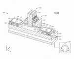
處理設備160包括一支撐件162及一處理單元164。支撐件162經設置在板120上且包括通過其的一開口166,該開口供工件台130在處理單元164下方通過。處理單元164被支撐件162支撐在板120上方。在一或更多個實施例中,處理單元164是經配置在光刻程序中曝光光阻劑的一圖案產生器。在一些實施例中,該圖案產生器經配置以進行無遮罩光刻程序。處理單元164包括複數個影像投射設備(顯示在第5圖中)。在一或更多個實施例中,處理單元164包含多達84個影像投射設備。各影像投射設備經設置在一殼體165中。處理設備160有用於對光阻劑或其他電磁輻射敏感材料進行無遮罩直接圖案寫入。The
在操作期間,工件台130從一負載位置(如第1圖中所示)在一X方向中移動至一處理位置。該處理位置是工件台130隨工件台130在處理單元164之下通過的一或更多個位置。在操作期間,工件台130從軌道124被複數個空氣軸承202(顯示在第2圖中)升舉,並在從軌道124被升起的同時從該負載位置沿該對軌道124移動至該處理位置。複數個垂直導引空氣軸承(未圖示)被耦接至工件台130且經定位鄰接各支撐件122的一內壁128以將工件台130的移動穩定化。工件台130也藉由沿著用於處理及/或定位(index)基板140的軌道150移動來在Y方向中移動。工件台130能夠獨立操作且能在一方向掃描基板140且在另一方向步進。During operation, the workpiece table 130 moves in an X direction from a loading position (shown in FIG. 1 ) to a processing position. The processing position is one or more positions at which the workpiece table 130 passes under the
一計量系統即時測量工件台130的X及Y橫向位置座標(每個工件台的),使得複數個影像投射設備中之各者能準確地定位要寫入的圖案到覆蓋有光阻劑之基板的正確位置。該計量系統也提供工件台130圍繞垂直或Z軸之角位置的即時測量。角位置的測量能被用以在藉由伺服機構掃描的期間保持工件台130的角位置不變,或者能被用以對將由影像投射設備270(第5圖中所示)寫到基板140上的圖案的位置施加校正。這些技術能結合使用。A metrology system measures the X and Y lateral position coordinates of the workpiece stages 130 (of each stage) in real time, enabling each of the plurality of image projection devices to accurately position the pattern to be written onto the photoresist-covered substrate the correct position. The metrology system also provides instant measurement of the angular position of the workpiece table 130 about the vertical or Z-axis. The measurement of the angular position can be used to maintain the angular position of the
第2圖是按照一或更多個實施例第1圖之處理系統100的截面側視圖。如上討論的,各工件台130包括複數個空氣軸承202以供升舉工件台130。各工件台130也可包括一致動器(像是馬達)以用於沿軌道124移動工件台130。兩個或更多個工件台130及處理設備160可經一外殼(未圖示)包圍以提供溫度及壓力控制。Figure 2 is a cross-sectional side view of the
系統100也包括一控制器190。控制器190概略經設計以促進本文所述處理技術的控制與自動化。控制器190可耦接至處理設備160、工件台130與編碼器126中一或更多者或與其通訊。處理設備160及工件台130可提供相關於基板處理及基板對準的資訊給控制器190。例如,處理設備160可提供資訊至控制器190以通知控制器190已完成基板處理。
控制器190可包括一中央處理單元(CPU)192、記憶體194、及支援電路(或I/O)196。CPU可為使用在工業設定中以供控制各種程序及硬體(例如圖案產生器、馬達及其他硬體)和監測程序(例如處理時間及基板位置)的任意形式電腦處理器之一者。記憶體194連接至CPU 192,且可為一或更多個隨時可得之記憶體,像是隨機存取記憶體(RAM)、唯讀記憶體(ROM)、軟碟、硬碟、或任何其他形式的數位儲存器,無論本機的或遠端的。能將軟體指令及資料編碼並儲存在記憶體194內以供指示CPU 192。支援電路196也連接至CPU以供用習知方式支援該處理器。該等支援電路可包括習用的快取、電源供應、時脈電路、輸入/輸出電路系統、子系統、及類似者。該控制器可讀取的程式(或電腦指令)決定哪些任務在基板上為可進行的。程式可為能由控制器讀取的軟體,並可包括代碼以監測及控制(例如)處理時間及基板位置。The
第3圖是可在按照一或更多個實施例之處理系統100中使用的複數個習用影像投射系統301的透視圖。如第3圖所示,各影像投射系統301製造到基板140之表面304上的複數個寫入光束302。隨基板140在x方向及y方向中移動,整個表面304可被寫入光束302形成圖案。影像投射系統301的個數可基於基板140的大小及/或工件台130的速度而異。Figure 3 is a perspective view of a plurality of conventional
第4A圖是按照一或更多個實施例第3圖中描繪之複數個影像投射系統301中之一習用影像投射系統301的透視示意圖。影像投射系統301可有一或更多光源402、光圈404、透鏡406、反射鏡408、數位微反射鏡裝置(DMD)410、光傾洩器(light dump)412、照相機414、及投射透鏡416。光源402可為LED或雷射。光源402能夠製造具有預定波長的光。在一或更多個實施例中,該預定波長是在藍光或近紫外光(UV)範圍中(像是小於大約450nm)。反射鏡408可為球面或其他適當的反射鏡。投射透鏡416可為10X接物透鏡。投射透鏡416可替代地具有其他放大率。Figure 4A is a schematic perspective view of a conventional
在操作期間,具有預定波長(像是在藍光範圍中的波長)的一光束403由光源402所製造。光束403被反射鏡408反射至DMD 410。During operation, a
DMD 410包括可經個別控制的複數個反射鏡,而DMD之複數個反射鏡中的各反射鏡可基於由控制器(未圖示)提供給該DMD的遮罩資料而於「開」位置抑或「關」位置。當光束403到達DMD 410的反射鏡時,位在「開」位置的反射鏡將光束403反射(例如形成複數個寫入光束302)至投射透鏡416。投射透鏡416接著將寫入光束302投射至基板140的表面304。位於「關」位置的反射鏡將光束403反射到光傾洩器412而非基板140的表面304。
按照一或更多個實施例,第4B圖描繪DMD 410的兩個反射鏡452、454。如所示,DMD 410的各反射鏡452、454經設置在一傾斜機構456上,該傾斜機構設置在一記憶體單元458上。在操作期間,各反射鏡452、454的控制是藉由將遮罩資料加載至該記憶體單元中。該遮罩資料以二進位方式靜電地控制反射鏡452、454的傾斜。當反射鏡452、454在重設模式中或未經施加電力時,其可被設定至未對應任何二進位數的平面位置。二進位的零可對應至「關」位置,其表示反射鏡傾斜-10度、-12度、或其他適當的負傾斜度。二進位的一可對應至「開」位置,其表示反射鏡傾斜+10度、+12度、或其他適當的正傾斜度。如第4B圖中顯示,反射鏡452位於「關」位置而反射鏡454位於「開」位置。Figure 4B depicts two
電流影像投射系統(像是影像投射系統301)苦受數種限制。例如,習用的影像投射系統受限於DMD 410中的各反射鏡僅可在「開」狀態與「關」狀態之間配置,因此僅提供兩種可能的曝光。額外地,習用的影像投射系統受限於DMD 410中的各反射鏡必須被移動定位至「開」抑或「關」狀態。例如,在操作期間有一準備時間,在準備時間期間用於各反射鏡的各記憶體單元458自一控制器接收資料,以在「開」位置抑或「關」位置之間切換。為此應用之目的,傳送指令至各記憶體單元458所花費的時間被稱為「資料加載」時間。在一些例子中,此可花費大約10微秒。除了資料加載時間之外,後續有花費時間來配置各反射鏡至開啟或關閉位置,例如「翻轉時間」(flip time)。各反射鏡必須基於被傳送給其個別記憶體單元458的指令而被帶至其正確位置中。在一些例子中,此花費大約10~15微秒。最後,也有一段時間在其間該系統在各反射鏡被帶至其正確位置中之後等待各反射鏡安定,例如「安定時間」(settling time)。此安定時間確保沒有機械性運動而產生的反射鏡之搖晃或震動。因此,對於各曝光有一總計準備時間為資料加載時間加上翻轉時間加上安定時間。由於各反射鏡必須經配置至一給定位置並經後續安定,因此唯一可改良的變數是資料加載時間,其可藉由更強的記憶體單元458來改良。然而,翻轉時間及安定時間仍將約束習用的影像投射系統。Current video projection systems such as
第5圖是按照一或更多個實施例供在處理系統100中使用的複數個改良影像投射系統500的透視圖。如第5圖中所示,各影像投射系統500製造複數個寫入光束502到基板140的表面504上。隨基板140在x方向及y方向中移動,整個表面504可被寫入光束502形成圖案。影像投射系統500的個數可基於基板140的大小及/或工件台130的速度而異。FIG. 5 is a perspective view of a plurality of improved
第6圖是按照一或更多個實施例第5圖之複數個影像投射系統500的一改良影像投射系統500的透視示意圖。影像投射系統500可包括一主動矩陣固態放射器顯示器(AMSSE)602、一照相機614、一焦點感測器616、一光學元件606、及一投射光學元件618。AMSSE 602包括至少複數個放射器元件(以下結合第7圖所討論及顯示),各放射器元件經配置以朝向基板140發出輻射604。放射器元件可為能夠發出輻射的任意足夠元件。在一或更多個實施例中,各放射器元件是一微放射器元件,像是二極體。因此,影像投射系統500不包括習用的機械組件(像是影像投射系統301的DMD 410),影像投射系統500也不包括一分離能量源402,因為各放射器元件是其自身的能量源。在一或更多個實施例中,影像投射系統500經配置以包括至少一個放射器元件,該至少一個放射器元件否則將是習用的影像投射系統301之DMD 410中的一個反射鏡。FIG. 6 is a schematic perspective view of an improved
在所顯示實施例中,光束604被朝向照相機614放射。照相機614與投射光學元件618類似以上結合第4A及4B圖討論的照相機414與投射透鏡416。在一或更多個實施例中,投射光學元件618是一投射透鏡。光學元件606經設置在AMSSE 602與照相機614之間。光學元件606供用於經傳輸至基板140之影像的視野大小縮減。在一或更多個實施例中,光學元件606是一透鏡。焦點感測器616可經設置在AMSSE 602與照相機614之間。在其他實施例中,焦點感測器616可經設置相鄰照相機614。焦點感測器616對影像投射系統500的對準及檢查提供反饋。在一或更多個實施例中,焦點感測器616包括一或更多輻射源,該一或更多輻射源經引導通過照相機614之透鏡並接著通過照相機614之透鏡返回且經成像在感測器上,以偵測是否從該等輻射源投射的光束點在光阻劑平面處聚焦。In the embodiment shown,
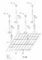
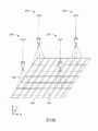
按照一或更多個實施例,第7A圖是第6圖之AMSSE 602的局部截面圖。AMSSE 602可經形成在一基板700上。在一或更多個實施例中,基板700可由藍寶石形成。一氮化鎵層702經沉積在基板700之上。矽層706經沉積在氮化鎵層702上。氮化鎵層702可包括p型氮化鎵層720、i型氮化鎵層722、及n型氮化鎵層724。一或更多電晶體704通過延伸進入氮化鎵層702中的複數個觸點726形成在矽層706中。複數個光修飾元件經定位在氮化鎵層702中。該複數個光修飾元件與氮化鎵層702一起被稱為一放射器基板711。例如,該等光修飾元件可包括以列與欄排列的複數個放射器708。各放射器708可為任何可配置以發射輻射的放射器。在一或更多例子中,各放射器708是微放射器。排列在一陣列中的一或更多放射器708,可界定一像素710。例如,放射器708可界定一1080p顯示畫面,其包含1920像素乘以1080像素的一陣列,總共大約2,073,600個像素。此例中2,073,600個像素的各像素可包含放射器708的一陣列。繼續此例,2,073,600個像素的各像素可對應至形成在矽層706中的一或更多電晶體704。在一些例子中,放射器708可界定一超高解析度(UHD)顯示畫面,其包含3840像素乘以2160像素的一陣列,總共8,294,400像素。一般,放射器708可界定任何適當的顯示畫面(例如UHD、1080p、720p、及類似者)。Figure 7A is a partial cross-sectional view of the
各放射器708可在「開」狀態與「關」狀態之間配置。在「開」狀態中,各放射器708可放射能量。此能量可為任意形式的電磁輻射。例如,在一或更多個實施例中,可使用所具波長在大約300nm到大約800nm之頻譜內的電磁輻射。在其他實施例中,也可使用此頻譜以外(例如紅外線、x射線、及類似者)的波長。在其他實施例中,該複數個放射器708之各放射器708具有不同波長。一控制器(像是控制器190)可將各放射器708配置成開啟狀態或關閉狀態。額外地,控制器190也可控制提供給放射器708的電流的量。因為不再需要機械地移動各放射器708(如先前使用DMD的習用影像投射系統所需要的),減去了翻轉時間及安定時間,因此縮短了整體的準備時間,因而改善了產量。額外地,各放射器708的強度可經調制以控制隨時間的曝光。傳統影像投射系統中,各反射鏡不是在「開」狀態就是在「關」狀態中;兩者之間沒有任何中間狀態。Each
按照一或更多個實施例,第7B圖是用於AMSSE 602的電路圖701。圖701包括一第一電晶體744a、一第二電晶體744b、及一放射器708。放射器708從第一電晶體744a及/或第二電晶體744b接收電流。在一些例子中,判斷哪些電晶體744a、744b是開或關的就決定了施加至對應於一像素之放射器陣列的電流量。可配置一像素來顯示各不同灰色色調,依照放射器所接收的電流而異。在一或更多個實施例中,各電晶體經配置以接收X與2X安培之間的電流。在一或更多個實施例中,提供給對應至像素之放射器708陣列的可能電流量為:3X安培(兩電晶體都是開)、2X安培(一個電晶體是開)、X(一個電晶體是開)、及0安培(兩電晶體都是關)。一個電晶體能接收的電流量依照該電晶體內閘極的寬度而定,使得閘極的寬度越寬則有更多電流能通過。在一或更多個實施例中,電晶體744a是開的且經配置以接收X安培的電流,而電晶體744b是開的且經配置以接收2X安培的電流,總共3X安培的總電流被施加至放射器708的陣列,該陣列對應於該像素的第一亮度。在其他實施例中,電晶體744a被關閉而電晶體744b被開啟接收2X安培的電流,總共2X安培的總電流被施加至放射器陣列,該陣列對應於該像素的第二亮度。在一些實施例中,電晶體744a被開啟並接收X安培的電流,同時電晶體744b被關閉,總共X安培的總電流被施加至放射器陣列,該陣列對應於該像素的第三亮度。在其他實施例中,各電晶體可經配置以接收有變化之電流量。概括先前的例子,各像素可經配置以顯示2n+1種灰色色調,其中n代表對應至該像素的電晶體個數。因此,AMSSE 602能夠獲得每像素灰階,其提供在像素可定址光刻系統的灰度(grey level)控制。在其他實施例中,各放射器可發射不同波長,使得產生的不是灰階而是色階。Figure 7B is a circuit diagram 701 for the
第7C圖是描繪按照一或更多個實施例用於AMSSE 602之一種配置方式的圖750。如所示,有單一金屬觸點740形成在p型氮化鎵層720中,該金屬觸點與放射器708電性連通。圖750包括三個電晶體(752a、752b、及752c)。電晶體752a經由連接線754a耦接至金屬觸點740。電晶體752b經由連接線754b耦接至金屬觸點740。電晶體752c經由連接線754c耦接至金屬觸點740。全部的電晶體752a~752c與金屬觸點740電接觸。因此,各電晶體752a~752c可提供可變量的信號至金屬觸點740。例如,提供給金屬觸點740的可變量的信號可為可變量的電壓、可變量的電流、或在高/低電線中為可變量。例如,電晶體752a經配置以提供100mA的電流;電晶體752b經配置以提供200mA的電流;電晶體752c經配置以提供400mA的電流。Figure 7C is a diagram 750 depicting one configuration for the
控制器190選擇地開啟/關閉各電晶體752a~752c。在一或更多例子中,控制器190僅開啟電晶體752a使得電流可流動至金屬觸點。繼續以上的例子,藉著僅電晶體752a在開啟位置中,金屬觸點740接收100mA的電流。在一些例子中,控制器190開啟電晶體752b及752c使得電流從電晶體752b流到金屬觸點740及從電晶體752c流到金屬觸點740。因此,電晶體752b及752c提供500mA的總電流給金屬觸點740。The
第7D圖是描繪按照一或更多個實施例用於AMSSE 602之一種配置方式的圖760。如所示,p型氮化鎵層720中界定有一金屬觸點範圍770。複數個金屬觸點772a~772c形成在金屬觸點範圍770中。例如,金屬觸點772a、772b、及772c經定位在金屬觸點範圍770中。圖760進一步包括三個電晶體(762a、762b、及762c)。電晶體762a經由連接線764a耦接至金屬觸點772a。電晶體762b經由連接線764b耦接至金屬觸點772b。電晶體762c經由連接線764c耦接至金屬觸點772c。全部的電晶體762a~762c都與金屬觸點740電接觸。因此,各電晶體762a~762c可對其個別的金屬觸點772a~772c提供可變量的信號。例如,電晶體762a經配置以提供100mA的電流至金屬觸點772a;電晶體762b經配置以提供200mA的電流至金屬觸點772b;電晶體762c經配置以提供400mA的電流至金屬觸點772c。儘管金屬觸點範圍770包括複數個金屬觸點772a~772c,金屬觸點772a~772c在光學上視為單一放射器,因此允許可變電流。Figure 7D is a diagram 760 depicting one configuration for the
控制器190選擇地開啟/關閉各電晶體762a~762c。在一或更多例子中,控制器190僅開啟電晶體762a使得電流可流動至觸點772a。繼續以上的例子,藉著僅電晶體762a在開啟位置中,金屬觸點772a接收100mA的電流。在一些例子中,控制器190開啟電晶體762b及762c使得電流從電晶體762b流到金屬觸點772b及從電晶體762c流到金屬觸點772c。因此,電晶體762b及762c提供500mA的總電流給金屬觸點範圍770。The
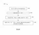
第8圖是按照一或更多個實施例,藉改良影像投射系統(像是以上第5-7B圖中揭示者)曝光基板的方法800。該方法開始於方塊802。於方塊802,AMSSE 602從控制器190接收指令,該指令包括曝光圖案。例如,控制器190指示AMSSE 602有關哪些放射器應在「開」位置中(例如控制器190指示AMSSE 602有關哪些放射器708將是開或關),基於所接收的曝光圖案。例如,控制器190可藉由選擇地選出哪些放射器708可被開啟或關閉,來產生放射器708的形狀。放射器708之形狀指的是針對曝光程序要開啟哪些放射器708至「開」狀態的圖案。繼續此例,給定nxm個放射器排列方式,控制器190可選擇地開啟n x m放射器708中的100 x 20子集合,以得到一細長矩形。在另一例中控制器可選擇地開啟放射器708以得到一圓形圖案或其他所欲的圖案。基本上,使用者可在不需改變AMSSE 602中放射器708之排列方式之下改變從AMSSE 602發射之輻射的形狀。Figure 8 is a
於方塊804,基板140的第一部分經曝光。曝光基板140可在基板140形成圖案來曝光基板140上的光阻劑。各曝光可持續的時間長在從大約2微秒到大約85微秒的範圍中,例如從大約5微秒到大約75微秒。例如,控制器可脈衝激發各放射器在開啟狀態中,以曝光基板140的第一部分。脈衝激發(pulse)可經界定為具有開始點及終止點,其中開始點及終止點具有兩者之間的持續時間。例如,該持續時間可能短至數秒或更短,長至數天或更久的時間。At
於方塊806,基板140經平移一步階大小,而基板140的第二部分經曝光。各曝光可持續的時間長在從大約2微秒到大約85微秒的範圍中,例如從大約5微秒到大約75微秒。例如,控制器可脈衝激發各放射器在開啟狀態中,以曝光基板140的第一部分。在一些實施例中,不是將基板140平移一步階大小,而是在維持基板140不動的同時將AMSSE 602平移一步階大小。At
於方塊808,重複將基板平移一步階大小與將基板的第二部分曝光至第二次電磁輻射射擊的程序,直到基板完全被處理為止。各曝光可產生一資料集,該資料集有關在基板140上被形成圖案的圖形對象。各資料集可經儲存在控制器的記憶體。各資料集可經組合以形成基板140上的影像圖案。各曝光可形成基板140之一部分的空拍影像。At
第9圖是按照一或更多個實施例,藉一改良影像投射系統(像是如上揭露在第5~7B圖中者)來曝光一基板的一方法900。該方法開始於方塊902。於方塊902,AMSSE 602從控制器190接收指令,該指令包括曝光圖案。例如,控制器190指示AMSSE 602有關哪些放射器708應在「開」位置中(例如控制器190指示AMSSE 602有關哪些放射器708將是開或關),基於所接收的曝光圖案。例如,控制器190可藉由選擇地選出哪些放射器708可被開啟或關閉,來產生放射器708的形狀。放射器的形狀指的是針對曝光程序要開啟哪些放射器708至「開」狀態的圖案。繼續此例,給定n x m個放射器708排列方式,控制器190可選擇地開啟n x m放射器708中的100 x 20子集合,以得到一細長矩形。在另一例中控制器可選擇地開啟放射器708以得到一圓形圖案,或其他所欲的圖案。基本上,使用者可在不需改變AMSSE 602中放射器708之排列方式之下改變從AMSSE 602發射之輻射的形狀。Figure 9 is a
於方塊904,AMSSE 602從控制器190接收指令,該等指令包括針對各放射器708之陣列的電晶體資訊。例如,給定用於界定第一像素之放射器708之第一陣列的第一組電晶體,AMSSE 602接收有關哪些電晶體將被開啟及哪些電晶體將被關閉的指令。利用此特定例子,當針對關聯於界定第一像素的放射器708之第一陣列的一組三個電晶體時,假設被送出的指令是全部三個電晶體將被開啟,則該第一像素將能顯示23=8種灰色色調。At
於方塊906,基板140的第一部分經曝光。曝光基板140可在基板140形成圖案來曝光基板140上的光阻劑。各曝光可持續在趨近大約2微秒與大約85微秒之間,例如在大約5微秒與大約75微秒之間。例如,控制器可脈衝激發各放射器708在開啟狀態中,以曝光基板140的第一部分。At
於方塊908,基板140經平移一步階大小,而基板140的第二部分經曝光。各曝光可持續在趨近大約2微秒與大約85微秒之間,例如在大約5微秒與大約75微秒之間。例如,控制器可脈衝激發各放射器708在開啟狀態中,以曝光基板140的第一部分。在一些實施例中,不是將基板140平移一步階大小,而是在維持基板140不動的同時將AMSSE 602平移一步階大小。At
於方塊910,重複將基板平移一步階大小與將基板的第二部分曝光至第二次電磁輻射射擊的程序,直到基板完全被處理為止。各曝光可產生一資料集,該資料集有關在基板140上被形成圖案的圖形對象。各資料集可經儲存在控制器的記憶體。各資料集可經組合以形成基板140上的影像圖案。各曝光可形成基板140之一部分的空拍影像。At
第10圖是按照一或更多個實施例,藉一改良影像投射系統(像是如上揭露在第5~7B圖中者)來曝光一基板的一方法1000。該方法開始於方塊1002。於方塊1002,AMSSE 602從控制器190接收指令,該指令包括曝光圖案。例如,控制器190指示AMSSE 602有關哪些放射器應在「開」位置中(例如控制器190指示AMSSE 602有關哪些放射器708將是開或關),基於所接收的曝光圖案。例如,控制器190可藉由選擇地選出哪些放射器708可被開啟或關閉,來產生放射器708的形狀。放射器的形狀指的是針對曝光程序要開啟哪些放射器708至「開」狀態的圖案。繼續此例,給定n x m個放射器708排列方式,控制器190可選擇地開啟n x m放射器708中的100 x 20子集合,以得到一細長矩形。在另一例中控制器可選擇地開啟放射器708以得到一圓形圖案,或其他所欲的圖案。基本上,使用者可在不需改變AMSSE 602中放射器708之排列方式之下改變從AMSSE 602發射之輻射的形狀。Figure 10 is a
於方塊1004,AMSSE 602從控制器190接收指令,該等指令包括針對各放射器708之陣列的電晶體資訊。例如,給定用於界定第一像素之放射器708之第一陣列的第一組電晶體,AMSSE 602接收有關哪些電晶體將被開啟及哪些電晶體將被關閉的指令。利用此特定例子,當針對關聯於界定第一像素的放射器708之第一陣列的一組三個電晶體時,假設被送出的指令是全部三個電晶體將被開啟,則該第一像素將能顯示23=8種灰色色調。At
於方塊1006,AMSSE 602自控制器190接收指令,該指令包括用於方塊1004中各電晶體的信號資訊。例如該信號資訊可包括將被施加至各電晶體或通過各電晶體的電流的量、電壓的量、或可變「開」狀態資訊。在一實施例中各放射器中的可變強度經選擇為一基極電流x的倍數。在另一實施例中各放射器中的可變強度乃選自x、2x、或3x。利用此特定例子,針對在方塊1004中所討論的該組三個電晶體,指令可包括由放射器拉動的450mA電流、同一放射器拉動的300mA、及同一放射器拉動的0mA。以此方式,一個放射器可經模製化已具有不同的灰色色調。因此,各像素可經驅動以傳達可變亮度。At
於方塊1008,基板140的第一部分經曝光。曝光基板140可在基板140形成圖案來曝光基板140上的光阻劑。各曝光可持續的時間長在從大約2微秒到大約85微秒的範圍中,例如從大約5微秒到大約50微秒。例如,控制器可脈衝激發各放射器在開啟狀態中,以曝光基板140的第一部分。At
於方塊1010,基板140經平移一步階大小,而基板140的第二部分經曝光。各曝光可在趨近大約2微秒與大約85微秒之間持續,例如在從大約5微秒到大約75微秒之間的範圍中。例如,控制器可脈衝激發各放射器在開啟狀態中,以曝光基板140的第一部分。在一實施例中各放射器經脈衝激發在開啟狀態中有一持續時間以曝光該基板的第一部分,該持續時間在從大約1奈秒到大約50微秒的範圍中。At
在一些實施例中,不是將基板140平移5mm或更低的步階大小,而是在維持基板140不動的同時將AMSSE 602平移一步階大小。In some embodiments, instead of translating the
於方塊1012,重複將基板平移一步階大小與將基板的第二部分曝光至第二次電磁輻射射擊的程序,直到基板完全被處理為止。各曝光可產生一資料集,該資料集有關在基板140上被形成圖案的圖形對象。各資料集可經儲存在控制器的記憶體中。各資料集可經組合以形成基板140上的影像圖案。各曝光可形成基板140之一部分的空拍影像。At
藉由允許每個像素的可變亮度,可利用該改良影像投射系統以得到相較於先前使用之基於DMD工具的改良光刻控制。例如,藉由有效運用像素的選擇性亮度,該改良影像投射系統能更佳地控制將被曝光之整個基板的均勻性。在一特定實施例中,終端使用者可校準各欄的驅動信號為具有不同亮度,用以校正整個基板上任何長程亮度變化。By allowing variable brightness per pixel, the improved image projection system can be utilized for improved lithographic control over previously used DMD-based tools. For example, by making efficient use of the selective brightness of pixels, the improved image projection system can better control the uniformity of the entire substrate to be exposed. In a specific embodiment, the end user can calibrate the drive signals for each column to have different brightness to correct for any long-term brightness variation across the substrate.
在一些例子中,藉由對各像素提供一不同信號來產生灰階效果,該改良影像投射系統允許終端使用者具有每像素之色階控制。此能輔助控制光刻特徵邊緣位置(feature edge placement)。額外地,此功能協助避免從整個基板上之階梯對角線產生的正交位址格線。藉著每像素亮度控制,藉由變化從各像素所發射之輻射的量,終端使用者能以此方式在基板曝光時控制「劑量」以避免階梯線。In some examples, the improved video projection system allows the end user to have per-pixel tone-scale control by providing a different signal to each pixel to produce a grayscale effect. This can assist in controlling lithographic feature edge placement. Additionally, this feature helps avoid orthogonal address grids arising from stepped diagonals across the substrate. By varying the amount of radiation emitted from each pixel by varying the amount of radiation emitted from each pixel through per-pixel brightness control, the end user can in this way control the "dose" when exposing a substrate to avoid step lines.
在一些例子中,對基板的不同區域可傳遞不同劑量,使得在光阻顯影之後,光阻劑被形成圖案成兩種不同深度。在基板經蝕刻至不同深度的一特定例子中,傳遞兩種不同劑量能在單一光刻步驟中藉由將像素劑量驅動至兩種不同位準而產生雙鑲嵌(dual damascene)圖案。In some examples, different doses may be delivered to different regions of the substrate such that after development of the photoresist, the photoresist is patterned to two different depths. In a specific example where the substrate is etched to different depths, delivering two different doses can create a dual damascene pattern in a single photolithography step by driving the pixel doses to two different levels.
在一些例子中,可在印刷條帶(swath)中利用該改良影像投射系統,在其中終端使用者需要確定相連條帶之間的拼接是混色的。此可藉由將像素的劑量從100%衰減至0%而經利用。In some instances, the improved image projection system can be utilized in printed swaths where the end user needs to assure that the stitching between adjacent swaths is color mixed. This can be exploited by attenuating the dose of a pixel from 100% to 0%.
儘管前述乃針對本揭示案之實施例,可設計出本揭示案的其他與進一步實施例而無悖離本揭示案的基本範疇,而本揭示案的範疇由以下的申請專利範圍所決定。Although the foregoing is directed to embodiments of the disclosure, other and further embodiments of the disclosure can be devised without departing from the basic scope of the disclosure, which is determined by the following claims.
100:系統100: system
110:底座框架110: base frame
112:空氣隔離器112: Air separator
120:板120: board
122:支撐件122: support
124:軌道124: track
126:編碼器126: Encoder
128:內壁128: inner wall
130:工件台130: work table
140:基板140: Substrate
150:軌道150: track
160:處理設備160: Processing equipment
162:支撐件162: support
164:處理單元164: processing unit
165:殼體165: shell
166:開口166: opening
190:控制器190: Controller
192:中央處理單元(CPU)192: Central Processing Unit (CPU)
194:記憶體194: memory
196:支援電路196: Support circuit
Claims (19)
Translated fromChineseApplications Claiming Priority (2)
| Application Number | Priority Date | Filing Date | Title |
|---|---|---|---|
| US15/933,147US10684555B2 (en) | 2018-03-22 | 2018-03-22 | Spatial light modulator with variable intensity diodes |
| US15/933,147 | 2018-03-22 |
Publications (2)
| Publication Number | Publication Date |
|---|---|
| TW201945838A TW201945838A (en) | 2019-12-01 |
| TWI784135Btrue TWI784135B (en) | 2022-11-21 |
Family
ID=67983224
Family Applications (1)
| Application Number | Title | Priority Date | Filing Date |
|---|---|---|---|
| TW108105386ATWI784135B (en) | 2018-03-22 | 2019-02-19 | Method, system, and non-transitory computer readable medium for producing image on substrate |
Country Status (7)
| Country | Link |
|---|---|
| US (1) | US10684555B2 (en) |
| EP (1) | EP3769155A4 (en) |
| JP (2) | JP7511474B2 (en) |
| KR (1) | KR102589768B1 (en) |
| CN (1) | CN111886543B (en) |
| TW (1) | TWI784135B (en) |
| WO (1) | WO2019182689A1 (en) |
Families Citing this family (3)
| Publication number | Priority date | Publication date | Assignee | Title |
|---|---|---|---|---|
| NO20190876A1 (en)* | 2019-07-11 | 2021-01-12 | Visitech As | Real time Registration Lithography system |
| CN111770244B (en)* | 2020-07-30 | 2022-10-04 | 哈尔滨方聚科技发展有限公司 | A non-modulated DMD spatial light modulator imaging method |
| US11880139B2 (en)* | 2021-09-23 | 2024-01-23 | Honeywell Federal Manufacturing & Technologies, Llc | Photolithography system including selective light array |
Citations (4)
| Publication number | Priority date | Publication date | Assignee | Title |
|---|---|---|---|---|
| CN106164777A (en)* | 2014-04-14 | 2016-11-23 | Asml荷兰有限公司 | The Optimizing Flow of photoetching process |
| TW201734663A (en)* | 2015-12-30 | 2017-10-01 | Asml荷蘭公司 | Method and apparatus for direct write maskless lithography |
| CN107425020A (en)* | 2009-06-17 | 2017-12-01 | 密执安州立大学董事会 | Radiation sensor |
| US20210307222A1 (en)* | 2020-03-31 | 2021-09-30 | Nippon Steel Chemical & Material Co., Ltd. | Carbon material filler for electromagnetic shield, electromagnetic shield material, and carbon-material-containing molded body for electromagnetic shield |
Family Cites Families (27)
| Publication number | Priority date | Publication date | Assignee | Title |
|---|---|---|---|---|
| US5043631A (en)* | 1988-08-23 | 1991-08-27 | Westinghouse Electric Corp. | Thin film electroluminescent edge emitter structure on a silicon substrate |
| JPH10294514A (en)* | 1997-04-17 | 1998-11-04 | Sharp Corp | Laser drive |
| JP3762091B2 (en)* | 1998-02-10 | 2006-03-29 | キヤノン株式会社 | Near-field photolithography method |
| JP2003251860A (en)* | 2001-12-27 | 2003-09-09 | Fuji Photo Film Co Ltd | Laser exposure system |
| JP3730573B2 (en)* | 2002-01-16 | 2006-01-05 | シャープ株式会社 | Exposure apparatus and image forming apparatus |
| DE10330135A1 (en)* | 2002-07-10 | 2004-01-22 | LumiLeds Lighting, U.S., LLC, San Jose | circuitry |
| WO2004013692A2 (en) | 2002-08-02 | 2004-02-12 | Massachusetts Institute Of Technology | System and method for maskless lithography using an array of sources and an array of focusing elements |
| DE10242142A1 (en) | 2002-09-03 | 2004-03-25 | Kleo Halbleitertechnik Gmbh & Co Kg | Manufacture of exposed structures using exposure apparatus, by reading macro line data sets for lines being exposed from memory while further macro lines are written to memory |
| JP2005072368A (en)* | 2003-08-26 | 2005-03-17 | Sony Corp | Semiconductor light emitting delement, semiconductor laser element, and image display device |
| JP2006091341A (en)* | 2004-09-22 | 2006-04-06 | Fuji Photo Film Co Ltd | Light source device for scanning exposure, scanning exposure method, and scanning exposure device |
| US7256867B2 (en) | 2004-12-22 | 2007-08-14 | Asml Netherlands B.V. | Lithographic apparatus and device manufacturing method |
| US9025136B2 (en) | 2008-09-23 | 2015-05-05 | Applied Materials, Inc. | System and method for manufacturing three dimensional integrated circuits |
| JP5294489B2 (en) | 2009-12-14 | 2013-09-18 | 株式会社ブイ・テクノロジー | Exposure method and exposure apparatus |
| TWI448830B (en)* | 2010-02-09 | 2014-08-11 | Asml Netherlands Bv | Lithographic apparatus and device manufacturing method |
| US9420653B2 (en)* | 2010-11-19 | 2016-08-16 | Semiconductor Components Industries, Llc | LED driver circuit and method |
| WO2012136434A2 (en)* | 2011-04-08 | 2012-10-11 | Asml Netherlands B.V. | Lithographic apparatus, programmable patterning device and lithographic method |
| KR101616761B1 (en)* | 2011-08-16 | 2016-04-29 | 에이에스엠엘 네델란즈 비.브이. | Lithographic apparatus, programmable patterning device and lithographic method |
| US9490239B2 (en)* | 2011-08-31 | 2016-11-08 | Micron Technology, Inc. | Solid state transducers with state detection, and associated systems and methods |
| US9001305B2 (en) | 2011-10-11 | 2015-04-07 | Wenhui Mei | Ultra-large size flat panel display maskless photolithography system and method |
| US10485066B2 (en)* | 2013-07-09 | 2019-11-19 | Ledvance Llc | Lamp with variable-beam output by discretely activating LED light sources |
| US20160266498A1 (en) | 2013-10-25 | 2016-09-15 | Asml Netherlands B.V. | Lithography apparatus, patterning device, and lithographic method |
| KR102427154B1 (en)* | 2014-08-01 | 2022-07-28 | 어플라이드 머티어리얼스, 인코포레이티드 | Digital grey tone lithography for 3d pattern formation |
| WO2016082941A1 (en)* | 2014-11-27 | 2016-06-02 | Carl Zeiss Smt Gmbh | Lithography apparatus comprising a plurality of individually controllable write heads |
| TWM550415U (en)* | 2016-01-28 | 2017-10-11 | 應用材料股份有限公司 | Image projection apparatus and system |
| US10908507B2 (en) | 2016-07-13 | 2021-02-02 | Applied Materials, Inc. | Micro LED array illumination source |
| CN109075185B (en) | 2016-07-13 | 2023-07-18 | 应用材料公司 | Micro LED array as illumination source |
| JP6678782B2 (en)* | 2016-07-19 | 2020-04-08 | エーエスエムエル ネザーランズ ビー.ブイ. | Apparatus for direct write maskless lithography |
- 2018
- 2018-03-22USUS15/933,147patent/US10684555B2/enactiveActive
- 2019
- 2019-02-05WOPCT/US2019/016601patent/WO2019182689A1/ennot_activeCeased
- 2019-02-05JPJP2020549761Apatent/JP7511474B2/enactiveActive
- 2019-02-05CNCN201980018636.XApatent/CN111886543B/enactiveActive
- 2019-02-05KRKR1020207030399Apatent/KR102589768B1/enactiveActive
- 2019-02-05EPEP19772405.7Apatent/EP3769155A4/ennot_activeWithdrawn
- 2019-02-19TWTW108105386Apatent/TWI784135B/enactive
- 2023
- 2023-04-05JPJP2023061225Apatent/JP7536939B2/enactiveActive
Patent Citations (4)
| Publication number | Priority date | Publication date | Assignee | Title |
|---|---|---|---|---|
| CN107425020A (en)* | 2009-06-17 | 2017-12-01 | 密执安州立大学董事会 | Radiation sensor |
| CN106164777A (en)* | 2014-04-14 | 2016-11-23 | Asml荷兰有限公司 | The Optimizing Flow of photoetching process |
| TW201734663A (en)* | 2015-12-30 | 2017-10-01 | Asml荷蘭公司 | Method and apparatus for direct write maskless lithography |
| US20210307222A1 (en)* | 2020-03-31 | 2021-09-30 | Nippon Steel Chemical & Material Co., Ltd. | Carbon material filler for electromagnetic shield, electromagnetic shield material, and carbon-material-containing molded body for electromagnetic shield |
Also Published As
| Publication number | Publication date |
|---|---|
| TW201945838A (en) | 2019-12-01 |
| KR20200124323A (en) | 2020-11-02 |
| JP7536939B2 (en) | 2024-08-20 |
| JP7511474B2 (en) | 2024-07-05 |
| EP3769155A4 (en) | 2021-12-15 |
| US10684555B2 (en) | 2020-06-16 |
| KR102589768B1 (en) | 2023-10-17 |
| JP2023098934A (en) | 2023-07-11 |
| EP3769155A1 (en) | 2021-01-27 |
| CN111886543A (en) | 2020-11-03 |
| US20190294051A1 (en) | 2019-09-26 |
| JP2021518577A (en) | 2021-08-02 |
| WO2019182689A1 (en) | 2019-09-26 |
| CN111886543B (en) | 2024-03-22 |
Similar Documents
| Publication | Publication Date | Title |
|---|---|---|
| JP7536939B2 (en) | Spatial light modulator with variable intensity diodes | |
| JP7271655B2 (en) | Keeping Spatial Light Modulator Sections in Spare to Address Field Non-Uniformities | |
| US10908507B2 (en) | Micro LED array illumination source | |
| KR102197572B1 (en) | Micro LED array as lighting source | |
| KR200492661Y1 (en) | Dmd with a long axis substantially perpendicular to the direction of scan | |
| CN112041751B (en) | Systems and methods using solid state emitter arrays | |
| JP7596139B2 (en) | Drawing device, drawing system, and drawing method | |
| CN112262346B (en) | Method for reducing data flow for spatial light modulator | |
| CN112020675B (en) | Fabrication and use of dose and feature size maps during substrate processing | |
| TW201812458A (en) | Direct imaging exposure apparatus and method |