TWI783154B - Determination method for defect of optical film, determination system for defect, and cutting system using the same - Google Patents
Determination method for defect of optical film, determination system for defect, and cutting system using the sameDownload PDFInfo
- Publication number
- TWI783154B TWI783154BTW108121331ATW108121331ATWI783154BTW I783154 BTWI783154 BTW I783154BTW 108121331 ATW108121331 ATW 108121331ATW 108121331 ATW108121331 ATW 108121331ATW I783154 BTWI783154 BTW I783154B
- Authority
- TW
- Taiwan
- Prior art keywords
- defect
- area
- value
- optical film
- gray scale
- Prior art date
Links
Images


Classifications
- G—PHYSICS
- G06—COMPUTING OR CALCULATING; COUNTING
- G06T—IMAGE DATA PROCESSING OR GENERATION, IN GENERAL
- G06T7/00—Image analysis
- G06T7/0002—Inspection of images, e.g. flaw detection
- G06T7/0004—Industrial image inspection
- G06T7/0006—Industrial image inspection using a design-rule based approach
- G—PHYSICS
- G06—COMPUTING OR CALCULATING; COUNTING
- G06T—IMAGE DATA PROCESSING OR GENERATION, IN GENERAL
- G06T7/00—Image analysis
- G06T7/10—Segmentation; Edge detection
- G06T7/11—Region-based segmentation
- G—PHYSICS
- G06—COMPUTING OR CALCULATING; COUNTING
- G06T—IMAGE DATA PROCESSING OR GENERATION, IN GENERAL
- G06T7/00—Image analysis
- G06T7/60—Analysis of geometric attributes
- G06T7/62—Analysis of geometric attributes of area, perimeter, diameter or volume
- G—PHYSICS
- G06—COMPUTING OR CALCULATING; COUNTING
- G06T—IMAGE DATA PROCESSING OR GENERATION, IN GENERAL
- G06T2207/00—Indexing scheme for image analysis or image enhancement
- G06T2207/10—Image acquisition modality
- G06T2207/10004—Still image; Photographic image
- G—PHYSICS
- G06—COMPUTING OR CALCULATING; COUNTING
- G06T—IMAGE DATA PROCESSING OR GENERATION, IN GENERAL
- G06T2207/00—Indexing scheme for image analysis or image enhancement
- G06T2207/30—Subject of image; Context of image processing
- G06T2207/30108—Industrial image inspection
Landscapes
- Engineering & Computer Science (AREA)
- Physics & Mathematics (AREA)
- Computer Vision & Pattern Recognition (AREA)
- General Physics & Mathematics (AREA)
- Theoretical Computer Science (AREA)
- Quality & Reliability (AREA)
- Geometry (AREA)
- Investigating Materials By The Use Of Optical Means Adapted For Particular Applications (AREA)
- Testing Of Optical Devices Or Fibers (AREA)
Abstract
Description
Translated fromChinese本發明是有關於一種缺陷判斷方法、缺陷判斷系統及使用其之切割系統,且特別是有關於一種光學膜之缺陷判斷方法、缺陷判斷系統及使用其之切割系統。The present invention relates to a defect judgment method, a defect judgment system and a cutting system using the same, and in particular to a defect judgment method of an optical film, a defect judgment system and a cutting system using the same.
習知光學膜在製作完成後通常需要分割成數條面積較小的光學膜。在分割後,必須以人工肉眼觀察方式,觀察切割後光學膜的斷面(側面)是否具有缺陷以及缺陷種類。然而,人工肉眼觀察方式容易造成誤判。因此,提出一種新的可增加判斷準確度的缺陷判斷技術是本技術領域業者努力的目標之一。Conventional optical films usually need to be divided into several optical films with smaller areas after they are fabricated. After the division, it is necessary to observe with the naked eye whether there is a defect and the type of the defect on the section (side surface) of the cut optical film. However, artificial naked eye observation is easy to cause misjudgment. Therefore, proposing a new defect judgment technology that can increase the judgment accuracy is one of the goals of the industry in this technical field.
本發明實施例提出一種光學膜之缺陷判斷方法、缺陷判斷系統及使用其之切割系統,可改善上述問題。Embodiments of the present invention provide a method for judging defects of an optical film, a defect judging system and a cutting system using the same, which can improve the above problems.
本發明一實施例提出一種光學膜之缺陷判斷方法。缺陷判斷方法包括以下步驟。擷取一光學膜之側面之一圖像,圖像包含一光學膜影像區及一背景區;取得光學膜影像區之一邊界基準線,圖像中位於邊界基準線上方的面積為一基準背景面積;取得基準背景面積相對於背景區之一背景區面積的一面積差值;以及,依據面積差值,判斷光學膜之一缺陷之類型。An embodiment of the present invention provides a method for judging defects of an optical film. The defect judgment method includes the following steps. Capture an image of the side of an optical film, the image contains a lightLearn the film image area and a background area; Obtain a boundary reference line of the optical film image area, and the area above the boundary reference line in the image is a reference background area; Obtain the ratio of the reference background area relative to the background area of the background area an area difference; and, according to the area difference, determine the type of a defect in the optical film.
本發明另一實施例提出一種光學膜之缺陷判斷系統。輸送系統包括一攝像器及一判斷器。攝像器用以擷取一光學膜之側面之一圖像,其中,圖像包含一光學膜影像區、一背景區及一缺陷區。判斷器用以:取得光學膜影像區之一邊界基準線,圖像中位於邊界基準線上方的面積為一基準背景面積;取得基準背景面積相對於背景區之一背景區面積的一面積差值;以及,依據面積差值,判斷光學膜之一缺陷之類型。Another embodiment of the present invention provides a defect judgment system for an optical film. The conveying system includes a camera and a judging device. The camera is used to capture an image of the side of an optical film, wherein the image includes an image area of the optical film, a background area and a defect area. The judging device is used to: obtain a border reference line of the image area of the optical film, and the area above the border reference line in the image is a reference background area; obtain an area difference between the reference background area and the background area of the background area; And, according to the area difference, determine the type of a defect in the optical film.
本發明另一實施例提出一種光學膜之切割系統。切割系統包括數個滾輪、一切割刀具及如前述之缺陷判斷系統。缺陷判斷系統之攝像器係鄰近於光學膜之側面配置。Another embodiment of the present invention provides an optical film cutting system. The cutting system includes several rollers, a cutting tool and the aforementioned defect judgment system. The camera of the defect judgment system is arranged adjacent to the side of the optical film.
為了對本發明之上述及其他方面有更佳的瞭解,下文特舉實施例,並配合所附圖式詳細說明如下:In order to have a better understanding of the above-mentioned and other aspects of the present invention, the following specific examples are given in detail with the accompanying drawings as follows:
10:光學膜10: Optical film
11:第一子光學膜11: The first sub-optical film
11s1、11s2、12s1、12s2:側面11s1, 11s2, 12s1, 12s2: side
12:第二子光學膜12: Second sub-optical film
20:切割系統20: Cutting system
21:滾輪21:Roller
22:切割刀具22: Cutting knife
23:雷射切割器23:Laser cutter
100:缺陷判斷系統100: Defect judgment system
110A~110D:攝像器110A~110D: camera
120:判斷器120:Judger
Ab:背景區面積Ab : area of background area
AL:基準背景面積AL : Reference background area
△A:面積差值△A: Area difference
D1:缺陷D1: defect
D1c:中心點D1c: center point
Gd,av:缺陷區平均灰階值Gd,av : Average gray scale value of defect area
Gf,av:影像區平均灰階值Gf,av : the average grayscale value of the image area
GL:灰階下限值GL : lower limit of gray scale
GU:灰階上限值GU : gray scale upper limit value
h1:距離h1: distance
L:邊界基準線L: boundary reference line
P:圖像P: Image
S110~S146B:步驟S110~S146B: steps
S:灰階值差異處S: Difference of gray scale value
T1:傳輸方向T1: Transmission direction
第1圖繪示依照本發明一實施例之光學膜之切割系統的示意圖。FIG. 1 shows a schematic diagram of an optical film cutting system according to an embodiment of the present invention.
第2圖繪示第1圖之缺陷判斷系統的功能方塊圖。FIG. 2 shows a functional block diagram of the defect judgment system in FIG. 1.
第3A~3C圖繪示第2圖之缺陷判斷系統之缺陷判斷方法的流程圖。3A-3C are flowcharts showing the defect judgment method of the defect judgment system in FIG. 2 .
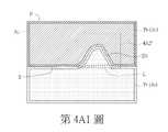
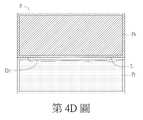
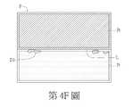
第4A1~4F圖繪示第1圖之光學膜可能發生的數種缺陷類型的圖像。Figures 4A1-4F show images of several types of defects that may occur in the optical film of Figure 1.
為了對本發明之上述及其他方面有更佳的瞭解,下文特舉實施例,並配合所附圖式詳細說明如下。In order to have a better understanding of the above and other aspects of the present invention, the following specific embodiments are described in detail in conjunction with the accompanying drawings.
請參照第1及2圖,第1圖繪示依照本發明一實施例之光學膜10之切割系統20的示意圖,而第2圖繪示第1圖之缺陷判斷系統100的功能方塊圖。Please refer to Figures 1 and 2. Figure 1 shows a schematic diagram of a
缺陷判斷系統100的缺陷判斷方法可採用對缺陷的特徵(如尺寸、灰階值)分類技術完成。例如,前述特徵分類技術係通過攝像器擷取待測物的完整圖像,此圖像是由許多圖元組成,每個圖元都有一定的灰階值(0~255)。因此,通過一定的數學、邏輯方法可對圖元資訊進行外觀分析,結構分析及幾何尺寸的計算,實現快速對待測物的各種檢測。在一實施例中,特徵分類技術例如是邊緣檢測法,而機器學習分類技術例如監督式學習,從給定的訓練資料集中學習出一個函式,當新的資料到來時,可以根據這個函式預測結果。以電腦進行特徵判斷缺陷類型,比人工判斷的方式更為準確。The defect judgment method of the
如第1圖所示,切割系統20包含數個滾輪21、切割刀具22及缺陷判斷系統100。此些滾輪21之一者鄰近切割刀具22配置。滾輪21可傳輸光學膜10經過切割刀具22,切割刀具22沿傳輸方向T1將光學膜10切割成(分離成)至少二條子光學膜,如第一子光學膜11及第二子光學膜12。在實施例中,切割刀具22例如是圓盤刀,其可透過旋轉運動切斷光學膜10。在一實施例中,切割系統20更包含雷射切割器23。滾輪21可傳輸光學膜10依序經過雷射切割器23及切割刀具22。雷射切割器23沿傳輸方向T1先對光學膜10進行半切割(不切穿光學膜10),然後,切割刀具22沿傳輸方向T1將光學膜10切割成(分離成)至少二條子光學膜,如第一子光學膜11及第二子光學膜12。As shown in FIG. 1 , the cutting
光學膜10可包含對光學之增益、配向、補償、轉向、直交、擴散、保護、防黏、耐刮、抗眩、反射抑制、高折射率等有所助益的膜,例如,可為偏光膜、離型膜、廣視角膜、增亮膜、反射膜、保護膜、具有控制視角補償或雙折射(birefraction)等特性的配向液晶膜、硬塗膜、抗反射膜、防黏膜、擴散膜、防眩膜等各種表面經處理的膜或上述之組合,但不限於此。
缺陷判斷系統100包含至少一攝像器(如攝像器110A~110D)及判斷器120。判斷器120例如是採用半導體製程所形成的電路結構。在一實施例中,判斷器120可整合於一處理器(processor)中。The
此些攝像器110A~110D之二者分別配置於一子光學膜斷面之相對二側,其中該相對二側之至少一者為切割側。在本實施例中,攝像器110A及110B分別鄰近子光學膜11之相對二側面11s1及11s2配置,且攝像器110A及110B分別鄰近子光學膜12之相對二側面12s1及12s2配置。在實施例中,攝像器110A~110D之照射方向與攝像器110A~110D正對光學膜側面之正對方向之間的夾角A1(第1圖僅以攝像器110B為例繪示)大致上介於±15°,較佳為±5°或0°。此外,當夾角A1為0°時,表示照射方向與正對方向重合;當夾角A1不為0°時,表示攝像器斜照光學膜之側面,即攝像器繞光學膜行進方向公轉後,照射方向與正對方向之間夾一不為0°的角度。The two
在一實施例中,切割系統20可更包括二切割刀具(圖未示),此二切割刀具分別切割出光學膜10之二邊條,二邊條分別自側面11s1及側面12s2分離。切割刀具可為圓盤刀或圓盤刀及雷射切割器併用。在此實施例中,側面11s1與11s2為切割側,且側面12s1與12s2也為切割側。此外,攝像器110A及110B分別朝向相對二側面11s1及11s2,以分別擷取相對二側11s1及11s2的圖像。相似地,攝像器110C及110D分別朝向相對二側面12s1及12s2,以分別擷取相對二側面12s1及12s2的圖像。In one embodiment, the cutting
在一實施例中,切割系統20可更包括二切割刀具(圖未示),此二切割刀具分別切割出光學膜10之二邊條(圖未示),二邊條分別自側面11s1及側面12s2分離。In one embodiment, the cutting
判斷器120用以分析攝像器110A~110D所擷取之圖像P,以判斷光學膜10的缺陷類型。以下係以第3A~3C圖及第4A1~4F圖說明第2圖之缺陷判斷系統100的缺陷判斷方法的流程。第3A~3C圖繪示第2圖之缺陷判斷系統100之缺陷判斷方法的流程圖,而第4A1~4F圖繪示第1圖之光學膜10可能發生的數種缺陷類型的圖像。The judging
如第4A1圖所示,圖像P之缺陷D1屬於凸膜型缺陷。如第4B1圖所示,圖像P之缺陷D1屬於毛屑型缺陷(例如是基於切割光學膜邊緣產生的毛屑)。如第4C圖所示,圖像P之缺陷D1屬於雷射起始點型缺陷(例如是基於使用雷射切割光學膜需求所產生的切割起始點缺陷)。如第4D圖所示,圖像P之缺陷D1屬於氣泡型缺陷(例如是基於多層光學膜貼合介面產生之氣泡)。如第4E圖所示,圖像P之缺陷D1屬於裂痕型缺陷。如第4F圖所示,圖像P之缺陷D1屬於髒污型缺陷。在另一實施例中,光學膜10的缺陷類型不限於前述6種,其可包含6種以上,或少於6種。As shown in FIG. 4A1, the defect D1 of the image P is a convex film defect. As shown in FIG. 4B1 , the defect D1 of the image P belongs to the dross type defect (for example, dross generated by cutting the edge of the optical film). As shown in FIG. 4C, the defect D1 of the image P belongs to the laser starting point defect (for example, it is a cutting starting point defect based on the requirement of cutting an optical film with a laser). As shown in Figure 4D, the defect D1 of the image P is a bubble-type defect (for example, bubbles generated at the bonding interface of the multilayer optical film). As shown in FIG. 4E, the defect D1 of the image P is a crack-type defect. As shown in FIG. 4F, the defect D1 of the image P is a dirty defect. In another embodiment, the defect types of the
在步驟S110中,數台攝像器110A~110D之至少一者擷取對應之子光學膜之側面的圖像。本發明實施例之缺陷判斷方法係以攝像器110C擷取第二子光學膜12之側面12s1之圖像為例說明,其餘攝像器110A、110B及110D擷取對應之子光學膜之側面之圖像皆可採用類似方法進行缺陷判斷,於此不再贅述。In step S110 , at least one of the plurality of
在步驟S110中,判斷器120分析所擷取的圖像P,並區分出圖像P之光學膜影像區Pf及背景區Pb,其中光學膜影像區Pf為攝像器110C所擷取的光學膜10的影像,而背景區Pb為攝像器110C所擷取的光學膜10以外的背景的影像。區分出圖像P之光學膜影像區Pf與背景區Pb之方式可採用二值化影像處理技術完成。以第4A1圖之圖像P舉例來說,判斷器120對圖像P進行二值化處理。二值化處理後,圖像P之光學膜影像區Pf之各像素點具有第一灰階值,於第4A1圖中以點剖面表示,而圖像P之背景區Pb之各像素點具有第二灰階值,於第4A1圖中以斜線剖面表示,其中第一灰階值與第二灰階值相異。如此,可透過灰階值差異區分出光學膜影像區Pf與背景區Pb。In step S110, the
在步驟S113中,如第4A1圖所示,判斷器120取得光學膜影像區Pf之邊界基準線L。例如,判斷器120以光學膜影像區Pf與背景區Pb之灰階值差異處S中相對變化「較緩和」之處的延伸做為邊界基準線L。前述「較緩和」的定義符合要件:灰階值差異處S=|Pf之第一灰階值-Pb之第二灰階值|,其中S>Pb之第二灰階值,S<Pf之第一灰階值,且S<(Pf之第一灰階值+Pb之第二灰階值)/2。邊界基準線L例如是光學膜10的外表面的輪廓線影像的延伸,即光學膜影像區Pf與背景區Pb之分界線。當圖像P無凸膜型缺陷(如第4A1圖)及毛屑型缺陷(如第4B1圖)時,光學膜影像區Pf之外表面輪廓線例如是直線,如第4C圖之圖像P中為水平線。In step S113 , as shown in FIG. 4A1 , the
取得邊界基準線L後,判斷器120計算圖像P之位於邊界基準線L上方之基準背景面積AL。以第4A1圖來說,背景區Pb及缺陷D1位於邊界基準線L上方,因此基準背景面積AL等於背景區Pb之背景區面積Ab與缺陷D1的面積之和。After obtaining the boundary reference line L, the
在步驟S115中,判斷器120取得基準背景面積AL相對於圖像P之背景區Pb之背景區面積Ab的面積差值△A。In step S115 , the
在另一實施例中,當邊界基準線L上方的基準背景面積AL與邊界基準線L下方的光學膜影像區Pf之光學區面積Af大致上相等時,判斷器120可取得光學膜影像區Pf之光學區面積Af相對於背景區Pb之背景區面積Ab之差值,並以此差值做為面積差值△A,其中若缺陷D1位於邊界基準線L上方,則光學區面積Af包含缺陷D1的面積。在此例子中,光學區面積Af相對於背景區Pb之背景區面積Ab之差值大致上等於缺陷D1的面積。In another embodiment, when the reference background area AL above the boundary reference line L is substantially equal to the optical zone area Af of the optical film image area Pf below the boundary reference line L, the
然而,本發明實施例不限定邊界基準線L的位置。依據攝像器與光學膜之側面的上下相對位置,邊界基準線L可位於圖像P的任何位置,且邊界基準線L之上、下區域面積可相等或相異。However, the embodiment of the present invention does not limit the position of the boundary reference line L. According to the vertical relative position of the camera and the side surface of the optical film, the boundary reference line L can be located at any position of the image P, and the area above and below the boundary reference line L can be equal or different.
在步驟S120中,判斷器120判斷面積差值△A是否大於第一面積預設值。當面積差值△A大於第一面積預設值,表示第一子光學膜11存在有缺陷D1且缺陷D1位於邊界基準線L上方,流程進入步驟S130,判斷器120判斷缺陷D1的類型,例如是判斷缺陷D1屬於第4A1圖之凸膜型缺陷或第4B1圖之毛屑型缺陷。此外,當缺陷D1位於邊界基準線L上方時,面積差值△A必為正值。In step S120, the
當面積差值△A不大於第一面積預設值,表示第一子光學膜11的缺陷D1不位於邊界基準線L上方(可能位於邊界基準線L下方),因此流程進入步驟S140,判斷器140接著判斷邊界基準線L下方的光學膜影像區Pf是否存在有缺陷D1,例如是否存在有第4C圖所示之雷射起始點型缺陷、第4D圖所示之氣泡型缺陷、如第4E圖所示之裂痕型缺陷或如第4F圖所示之髒污型缺陷。When the area difference ΔA is not greater than the first area preset value, it means that the defect D1 of the first
在一實施例中,前述第一面積預設值可以面積尺寸值或像素數量。以像素數量來說,例如是50點,然可依據像素數量換算成對應的尺寸值,或者依據尺寸值換算成對應的像素數量。In an embodiment, the aforementioned first area preset value may be an area size value or a number of pixels. In terms of the number of pixels, for example, 50 points, it can be converted into a corresponding size value according to the number of pixels, or converted into a corresponding number of pixels according to the size value.
位於邊界基準線L上方的缺陷類型判斷過程(步驟S130)可透過尺寸分析完成。以下係進一步舉例說明。The process of judging the defect type above the boundary reference line L (step S130 ) can be completed through size analysis. The following is a further example.
在步驟S131中,判斷器120判斷面積差值△A是否介於第一面積預設值與第二面積預設值之間,其中第二面積預設值大於第一面積預設值。以像素數量來說,第二面積預設值例如是200點。當面積差值△A介於第一面積預設值與第二面積預設值之間,表示缺陷D1可能是毛屑型缺陷,流程進入步驟S132A,進一步判斷缺陷D1是否屬於毛屑型缺陷;若否,表示缺陷D1可能是凸膜型缺陷,則流程進入步驟S133A,進一步判斷缺陷D1是否屬於凸膜型缺陷。In step S131 , the
在步驟S132A中,判斷器120判斷缺陷D1之第一方向尺寸是否小於第一尺寸預設值及缺陷D1之第二方向尺寸是否小於第二尺寸預設值。當缺陷D1之第一方向尺寸小於第一尺寸預設值及缺陷D1之第二方向尺寸小於第二尺寸預設值,判斷器120判定缺陷D1屬於毛屑型缺陷。以像素點來說,第一尺寸預設值及第二尺寸預設值例如是3點。缺陷D1之第一方向尺寸不小於第一尺寸預設值及缺陷D1之第二方向尺寸不小於第二尺寸預設值的情況(步驟S132A的「否」結果)於本發明實施例不會發生,因此本文不予討論。In step S132A, the
以第4B1及4B2圖舉例來說,判斷器120判定缺陷D1屬於毛屑型缺陷的方式例如是:取得缺陷D1沿第一方向(如X方向)的各Xi行的像素點數量(如X1~X3行各為2點);然後,判斷此些Xi行的最大像素點數量是否小於第一尺寸預設值,例如各Xi行的像素點數量皆等於2,其小於第一尺寸預設值(以3為例);然後,取得缺陷D1沿第二方向(如Y方向)的各Yi行的像素點數量(如Y1~Y4行分別為1、2、2及1點);然後,判斷此些Yi行的最大像素點數量是否小於第二尺寸預設值,例如Y2行具有最大像素點數量(即2),其小於第二尺寸預設值(以3為例)。據此,判斷器120判定第4B1圖之缺陷D1屬於毛屑型缺陷。Taking Figures 4B1 and 4B2 as an example, the way for the
在步驟S133A中,判斷器120判斷面積差值△A是否大於第二面積預設值。若是,表示缺陷D1可能屬於凸膜型缺陷(如第4A1圖所示),流程進入步驟S133B。In step S133A, the
在步驟S133B中,判斷器120判斷缺陷D1之第一方向尺寸是否等於或大於第一尺寸預設值及缺陷D1之第二方向尺寸是否等於或大於第二尺寸預設值。若是,流程進入步驟S133C,判斷器120判定缺陷D1屬於凸膜型缺陷(如第4A1圖所示)。缺陷D1之第一方向尺寸不等於或不大於第一尺寸預設值及缺陷D1之第二方向尺寸不等於或不大於第二尺寸預設值的情況(步驟S133B的「否」結果)於本發明實施例不會發生,因此本文不予討論。In step S133B, the
以第4A1及4A2圖舉例來說,判斷器120判定缺陷D1屬於凸膜型缺陷的方式例如是:取得缺陷D1沿第一方向(如X方向)的各Xi行的像素點數量(如X1~X3行分別為5、4及3點);然後,判斷此些Xi行的最大像素點數量是否小於第一尺寸預設值,例如X1行具有最大像素點數量(即5),其大於第一尺寸預設值(以3為例);然後,取得缺陷D1沿第二方向(如Y方向)的各Yi行的像素點數量(如Y1~Y5行分別為2、3、3、2及1點);然後,判斷此些Yi行的最大像素點數量是否小於第二尺寸預設值,例如Y3行具有最大像素點數量(即3),其等於第二尺寸預設值(以1為例)。據此,判斷器120判定第4A1圖所示之缺陷D1屬於凸膜型缺陷。Taking Figures 4A1 and 4A2 as an example, the method for judging that the defect D1 belongs to a convex-film defect by the
位於邊界基準線L下方的缺陷類型判斷過程(步驟S140)可透過灰階值分析完成。以下係進一步舉例說明。The defect type judgment process (step S140 ) located below the boundary reference line L can be completed through gray scale value analysis. The following is a further example.
在步驟S141中,判斷器120取得光學膜影像區Pf之缺陷D1的缺陷區平均灰階值Gd,av。詳言之,缺陷D1的像素灰階值與光學膜影像區Pf之缺陷D1以外區域的像素灰階值不同,因此判斷器120可透過光學膜影像區Pf之各像素的灰階值差異來判斷缺陷D1的分布區域,以及缺陷D1的分布區域的缺陷區平均灰階值Gd,av。In step S141 , the
在步驟S142中,判斷器120判斷缺陷平均灰階值Gd,av是否介於灰階下限值GL與灰階上限值GU之間。若是,流程進入步驟S144,判斷器120判定缺陷D1屬於髒污型缺陷。在一實施例中,灰階下限值GL例如是30,而灰階上限值GU例如是70(當灰階值為0時,顏色為黑色,而當灰階值為255時,顏色為白色)。以第4F圖舉例來說,由於髒汙的灰階值(顏色)範圍顏色大致上介於灰階下限值GL與灰階上限值GU之間。因此,當缺陷平均灰階值Gd,av介於灰階下限值GL與灰階上限值GU之間時,判斷器120判斷第4F圖之缺陷D1屬於髒污型缺陷。In step S142, the judging
在步驟S142中,當缺陷平均灰階值Gd,av未介於灰階下限值GL與灰階上限值GU之間,表示缺陷D1可能屬於雷射起始點缺陷(如第4C圖所示),流程進入步驟S143A,判斷器120進一步確認缺陷D1是否屬於雷射起始點缺陷。In step S142, when the defect average gray scale value Gd, av is not between the gray scale lower limit valueGL and the gray scale upper limit value GU , it means that the defect D1 may belong to the laser starting point defect (as in Section 4C As shown in the figure), the process enters step S143A, and the
在步驟S143A中,判斷器120判斷缺陷D1之缺陷區平均灰階值Gd,av是否小於灰階下限值GL。若是,則流程進入步驟S143B,再進一步判斷缺陷D1是否屬於雷射起始點型缺陷(如第4C圖所示);若否,表示缺陷D1可能屬於氣泡型缺陷(如第4D圖所示)或裂痕型缺陷(如第4E圖所示),則流程進入步驟S145A,進一步判斷缺陷D1屬於氣泡型缺陷或裂痕型缺陷。In stepS143A , the judging
在步驟S143B中,如第4C圖所示,判斷器120判斷光學膜影像區Pf之邊界基準線L與缺陷D1的中心點D1c之間的距離h1是否大於預設距離值。若是,則流程進入步驟S143C,判斷器120判定第4C圖所示之缺陷D1屬於雷射起始點型缺陷。在實施例中,預設距離值例如是200微米。若距離h1不大於預設距離值(步驟S143B的「否」結果),判斷器120判斷缺陷D1屬於其它類型缺陷。In step S143B, as shown in FIG. 4C , the
在步驟S145A中,判斷器120取得光學膜影像區Pf之影像區平均灰階值Gf,av。詳言之,判斷器120可分析光學膜影像區Pf之全區之各像素點的灰階值,並據以計算此些像素點的平均值,此平均值即影像區平均灰階值Gf,av。In step S145A, the judging
在步驟S145B中,判斷器120判斷缺陷區平均灰階值Gd,av是否大於影像區平均灰階值Gf,av。若是,流程進入步驟S145C。缺陷區平均灰階值Gd,av不大於影像區平均灰階值Gf,av的情況(步驟S145B的「否」結果)於本發明實施例不會發生,因此本文不予討論。In step S145B, the judging
在步驟S145C中,判斷器120判斷缺陷區平均灰階值Gd,av是否小於灰階下限值GL。若否,流程進入步驟S145D,判斷器120判定缺陷D1屬於氣泡型缺陷(如第4D圖所示)。當缺陷區平均灰階值Gd,av不小於灰階下限值GL,流程進入步驟S146A。In stepS145C , the judging
在步驟S146A中,判斷器120判斷光學膜影像區Pf之邊界基準線L與缺陷D1的中心點D1c之間的距離h1是否大於預設距離。若是,流程進入步驟S146B。若否,則判斷器120判斷缺陷D1屬於其它類型缺陷。In step S146A, the judging
在步驟S146B中,判斷器120判定缺陷D1屬於裂痕型缺陷(如第4E圖所示)。In step S146B, the
綜上所述,雖然本發明已以實施例揭露如上,然其並非用以限定本發明。本發明所屬技術領域中具有通常知識者,在不脫離本發明之精神和範圍內,當可作各種之更動與潤飾。因此,本發明之保護範圍當視後附之申請專利範圍所界定者為準。To sum up, although the present invention has been disclosed by the above embodiments, it is not intended to limit the present invention. Those skilled in the art of the present invention can make various changes and modifications without departing from the spirit and scope of the present invention. Therefore, the scope of protection of the present invention should be defined by the scope of the appended patent application.
S110~S133C:步驟S110~S133C: steps
Claims (19)
Translated fromChinesePriority Applications (2)
| Application Number | Priority Date | Filing Date | Title |
|---|---|---|---|
| TW108121331ATWI783154B (en) | 2019-06-19 | 2019-06-19 | Determination method for defect of optical film, determination system for defect, and cutting system using the same |
| CN202010293850.0ACN111507955B (en) | 2019-06-19 | 2020-04-15 | Defect judging method and defect judging system for optical film |
Applications Claiming Priority (1)
| Application Number | Priority Date | Filing Date | Title |
|---|---|---|---|
| TW108121331ATWI783154B (en) | 2019-06-19 | 2019-06-19 | Determination method for defect of optical film, determination system for defect, and cutting system using the same |
Publications (2)
| Publication Number | Publication Date |
|---|---|
| TW202101381A TW202101381A (en) | 2021-01-01 |
| TWI783154Btrue TWI783154B (en) | 2022-11-11 |
Family
ID=71864111
Family Applications (1)
| Application Number | Title | Priority Date | Filing Date |
|---|---|---|---|
| TW108121331ATWI783154B (en) | 2019-06-19 | 2019-06-19 | Determination method for defect of optical film, determination system for defect, and cutting system using the same |
Country Status (2)
| Country | Link |
|---|---|
| CN (1) | CN111507955B (en) |
| TW (1) | TWI783154B (en) |
Citations (4)
| Publication number | Priority date | Publication date | Assignee | Title |
|---|---|---|---|---|
| CN104792794A (en)* | 2015-04-28 | 2015-07-22 | 武汉工程大学 | Machine vision based optical film surface defect detecting method |
| US9582872B2 (en)* | 2015-07-03 | 2017-02-28 | Yuan Ze University | Optical film defect detection method and system thereof |
| TWI583476B (en)* | 2012-12-18 | 2017-05-21 | 住友化學股份有限公司 | Production method of optical display device and production system of optical display device |
| TW201741650A (en)* | 2016-05-24 | 2017-12-01 | Lg化學股份有限公司 | The system and method of detecting defect of optical film |
Family Cites Families (2)
| Publication number | Priority date | Publication date | Assignee | Title |
|---|---|---|---|---|
| WO2008144751A1 (en)* | 2007-05-21 | 2008-11-27 | Cornell University | Method for segmenting objects in images |
| CN109387525A (en)* | 2017-08-09 | 2019-02-26 | 苏州精濑光电有限公司 | On a kind of film in film defect determination method |
- 2019
- 2019-06-19TWTW108121331Apatent/TWI783154B/enactive
- 2020
- 2020-04-15CNCN202010293850.0Apatent/CN111507955B/enactiveActive
Patent Citations (4)
| Publication number | Priority date | Publication date | Assignee | Title |
|---|---|---|---|---|
| TWI583476B (en)* | 2012-12-18 | 2017-05-21 | 住友化學股份有限公司 | Production method of optical display device and production system of optical display device |
| CN104792794A (en)* | 2015-04-28 | 2015-07-22 | 武汉工程大学 | Machine vision based optical film surface defect detecting method |
| US9582872B2 (en)* | 2015-07-03 | 2017-02-28 | Yuan Ze University | Optical film defect detection method and system thereof |
| TW201741650A (en)* | 2016-05-24 | 2017-12-01 | Lg化學股份有限公司 | The system and method of detecting defect of optical film |
Also Published As
| Publication number | Publication date |
|---|---|
| CN111507955B (en) | 2024-03-08 |
| CN111507955A (en) | 2020-08-07 |
| TW202101381A (en) | 2021-01-01 |
Similar Documents
| Publication | Publication Date | Title |
|---|---|---|
| CN110473179B (en) | Method, system and equipment for detecting surface defects of thin film based on deep learning | |
| CN108760747B (en) | A visual inspection method for surface defects of 3D printing models | |
| CN105067638B (en) | Tire fetal membrane face character defect inspection method based on machine vision | |
| US6512239B1 (en) | Stereo vision inspection system for transparent media | |
| CN108764345B (en) | A crack detection method for underwater dams based on local and global clustering | |
| CN115311294B (en) | Glass bottle body flaw identification and detection method based on image processing | |
| CN115100200B (en) | Optical fiber defect detection method and system based on optical means | |
| WO2001081904A1 (en) | Dark view inspection system for transparent media | |
| US9594021B2 (en) | Apparatus of detecting transmittance of trench on infrared-transmittable material and method thereof | |
| CN114926407A (en) | Steel surface defect detection system based on deep learning | |
| TWI714923B (en) | Automated optical inspection system and automated optical inspection method using the same | |
| CN115546170B (en) | Fan blade defect positioning method and system based on laser ranging | |
| CN104568987A (en) | Method for inspecting transparent body, and apparatus for inspecting transparent body | |
| CN108469437B (en) | Method and device for detecting defects of float glass | |
| CN114119591A (en) | A kind of display screen picture quality detection method | |
| CN114858805A (en) | Glass coated surface defect online detection device and defect classification identification method | |
| CN106872488A (en) | A kind of double surface defect visible detection methods of rapid large-area transparent substrate and device | |
| CN104237246A (en) | Defect identification method of optical thin film | |
| CN116026861A (en) | Method and system for detecting glass bottles | |
| TWI783154B (en) | Determination method for defect of optical film, determination system for defect, and cutting system using the same | |
| CN106770372B (en) | Detection method of white glass surface defects based on microscopic vision | |
| TWI771594B (en) | Training method for defect and system using same, and determent method for defect and system using same | |
| EP3974817A1 (en) | Non-lambertian surface inspection system for line scan | |
| TW201617605A (en) | Defect inspection method and apparatus thereof | |
| CN120031791A (en) | A two-stage tool surface defect detection method and system |