TWI782573B - In-memory computation device and in-memory computation method - Google Patents
In-memory computation device and in-memory computation methodDownload PDFInfo
- Publication number
- TWI782573B TWI782573BTW110121220ATW110121220ATWI782573BTW I782573 BTWI782573 BTW I782573BTW 110121220 ATW110121220 ATW 110121220ATW 110121220 ATW110121220 ATW 110121220ATW I782573 BTWI782573 BTW I782573B
- Authority
- TW
- Taiwan
- Prior art keywords
- memory
- memory cell
- bits
- bit lines
- input
- Prior art date
Links
Images


Classifications
- G—PHYSICS
- G06—COMPUTING OR CALCULATING; COUNTING
- G06F—ELECTRIC DIGITAL DATA PROCESSING
- G06F7/00—Methods or arrangements for processing data by operating upon the order or content of the data handled
- G06F7/38—Methods or arrangements for performing computations using exclusively denominational number representation, e.g. using binary, ternary, decimal representation
- G06F7/48—Methods or arrangements for performing computations using exclusively denominational number representation, e.g. using binary, ternary, decimal representation using non-contact-making devices, e.g. tube, solid state device; using unspecified devices
- G06F7/544—Methods or arrangements for performing computations using exclusively denominational number representation, e.g. using binary, ternary, decimal representation using non-contact-making devices, e.g. tube, solid state device; using unspecified devices for evaluating functions by calculation
- G06F7/5443—Sum of products
- G—PHYSICS
- G11—INFORMATION STORAGE
- G11C—STATIC STORES
- G11C11/00—Digital stores characterised by the use of particular electric or magnetic storage elements; Storage elements therefor
- G11C11/21—Digital stores characterised by the use of particular electric or magnetic storage elements; Storage elements therefor using electric elements
- G11C11/34—Digital stores characterised by the use of particular electric or magnetic storage elements; Storage elements therefor using electric elements using semiconductor devices
- G11C11/40—Digital stores characterised by the use of particular electric or magnetic storage elements; Storage elements therefor using electric elements using semiconductor devices using transistors
- G11C11/401—Digital stores characterised by the use of particular electric or magnetic storage elements; Storage elements therefor using electric elements using semiconductor devices using transistors forming cells needing refreshing or charge regeneration, i.e. dynamic cells
- G11C11/4063—Auxiliary circuits, e.g. for addressing, decoding, driving, writing, sensing or timing
- G11C11/407—Auxiliary circuits, e.g. for addressing, decoding, driving, writing, sensing or timing for memory cells of the field-effect type
- G11C11/409—Read-write [R-W] circuits
- G11C11/4093—Input/output [I/O] data interface arrangements, e.g. data buffers
- G—PHYSICS
- G06—COMPUTING OR CALCULATING; COUNTING
- G06F—ELECTRIC DIGITAL DATA PROCESSING
- G06F7/00—Methods or arrangements for processing data by operating upon the order or content of the data handled
- G06F7/38—Methods or arrangements for performing computations using exclusively denominational number representation, e.g. using binary, ternary, decimal representation
- G06F7/48—Methods or arrangements for performing computations using exclusively denominational number representation, e.g. using binary, ternary, decimal representation using non-contact-making devices, e.g. tube, solid state device; using unspecified devices
- G06F7/50—Adding; Subtracting
- G06F7/501—Half or full adders, i.e. basic adder cells for one denomination
- G—PHYSICS
- G06—COMPUTING OR CALCULATING; COUNTING
- G06F—ELECTRIC DIGITAL DATA PROCESSING
- G06F7/00—Methods or arrangements for processing data by operating upon the order or content of the data handled
- G06F7/38—Methods or arrangements for performing computations using exclusively denominational number representation, e.g. using binary, ternary, decimal representation
- G06F7/48—Methods or arrangements for performing computations using exclusively denominational number representation, e.g. using binary, ternary, decimal representation using non-contact-making devices, e.g. tube, solid state device; using unspecified devices
- G06F7/52—Multiplying; Dividing
- G06F7/523—Multiplying only
- G—PHYSICS
- G11—INFORMATION STORAGE
- G11C—STATIC STORES
- G11C11/00—Digital stores characterised by the use of particular electric or magnetic storage elements; Storage elements therefor
- G11C11/21—Digital stores characterised by the use of particular electric or magnetic storage elements; Storage elements therefor using electric elements
- G11C11/34—Digital stores characterised by the use of particular electric or magnetic storage elements; Storage elements therefor using electric elements using semiconductor devices
- G11C11/40—Digital stores characterised by the use of particular electric or magnetic storage elements; Storage elements therefor using electric elements using semiconductor devices using transistors
- G11C11/401—Digital stores characterised by the use of particular electric or magnetic storage elements; Storage elements therefor using electric elements using semiconductor devices using transistors forming cells needing refreshing or charge regeneration, i.e. dynamic cells
- G11C11/4063—Auxiliary circuits, e.g. for addressing, decoding, driving, writing, sensing or timing
- G11C11/407—Auxiliary circuits, e.g. for addressing, decoding, driving, writing, sensing or timing for memory cells of the field-effect type
- G11C11/408—Address circuits
- G11C11/4085—Word line control circuits, e.g. word line drivers, - boosters, - pull-up, - pull-down, - precharge
- G—PHYSICS
- G11—INFORMATION STORAGE
- G11C—STATIC STORES
- G11C11/00—Digital stores characterised by the use of particular electric or magnetic storage elements; Storage elements therefor
- G11C11/21—Digital stores characterised by the use of particular electric or magnetic storage elements; Storage elements therefor using electric elements
- G11C11/34—Digital stores characterised by the use of particular electric or magnetic storage elements; Storage elements therefor using electric elements using semiconductor devices
- G11C11/40—Digital stores characterised by the use of particular electric or magnetic storage elements; Storage elements therefor using electric elements using semiconductor devices using transistors
- G11C11/401—Digital stores characterised by the use of particular electric or magnetic storage elements; Storage elements therefor using electric elements using semiconductor devices using transistors forming cells needing refreshing or charge regeneration, i.e. dynamic cells
- G11C11/4063—Auxiliary circuits, e.g. for addressing, decoding, driving, writing, sensing or timing
- G11C11/407—Auxiliary circuits, e.g. for addressing, decoding, driving, writing, sensing or timing for memory cells of the field-effect type
- G11C11/409—Read-write [R-W] circuits
- G11C11/4091—Sense or sense/refresh amplifiers, or associated sense circuitry, e.g. for coupled bit-line precharging, equalising or isolating
- G—PHYSICS
- G11—INFORMATION STORAGE
- G11C—STATIC STORES
- G11C11/00—Digital stores characterised by the use of particular electric or magnetic storage elements; Storage elements therefor
- G11C11/21—Digital stores characterised by the use of particular electric or magnetic storage elements; Storage elements therefor using electric elements
- G11C11/34—Digital stores characterised by the use of particular electric or magnetic storage elements; Storage elements therefor using electric elements using semiconductor devices
- G11C11/40—Digital stores characterised by the use of particular electric or magnetic storage elements; Storage elements therefor using electric elements using semiconductor devices using transistors
- G11C11/401—Digital stores characterised by the use of particular electric or magnetic storage elements; Storage elements therefor using electric elements using semiconductor devices using transistors forming cells needing refreshing or charge regeneration, i.e. dynamic cells
- G11C11/4063—Auxiliary circuits, e.g. for addressing, decoding, driving, writing, sensing or timing
- G11C11/407—Auxiliary circuits, e.g. for addressing, decoding, driving, writing, sensing or timing for memory cells of the field-effect type
- G11C11/409—Read-write [R-W] circuits
- G11C11/4094—Bit-line management or control circuits
- G—PHYSICS
- G11—INFORMATION STORAGE
- G11C—STATIC STORES
- G11C7/00—Arrangements for writing information into, or reading information out from, a digital store
- G11C7/10—Input/output [I/O] data interface arrangements, e.g. I/O data control circuits, I/O data buffers
- G11C7/1006—Data managing, e.g. manipulating data before writing or reading out, data bus switches or control circuits therefor
- G—PHYSICS
- G06—COMPUTING OR CALCULATING; COUNTING
- G06F—ELECTRIC DIGITAL DATA PROCESSING
- G06F2207/00—Indexing scheme relating to methods or arrangements for processing data by operating upon the order or content of the data handled
- G06F2207/38—Indexing scheme relating to groups G06F7/38 - G06F7/575
- G06F2207/48—Indexing scheme relating to groups G06F7/48 - G06F7/575
- G06F2207/4802—Special implementations
- G06F2207/4814—Non-logic devices, e.g. operational amplifiers
- G—PHYSICS
- G06—COMPUTING OR CALCULATING; COUNTING
- G06N—COMPUTING ARRANGEMENTS BASED ON SPECIFIC COMPUTATIONAL MODELS
- G06N3/00—Computing arrangements based on biological models
- G06N3/02—Neural networks
- G06N3/06—Physical realisation, i.e. hardware implementation of neural networks, neurons or parts of neurons
- G06N3/063—Physical realisation, i.e. hardware implementation of neural networks, neurons or parts of neurons using electronic means
- G—PHYSICS
- G11—INFORMATION STORAGE
- G11C—STATIC STORES
- G11C11/00—Digital stores characterised by the use of particular electric or magnetic storage elements; Storage elements therefor
- G11C11/54—Digital stores characterised by the use of particular electric or magnetic storage elements; Storage elements therefor using elements simulating biological cells, e.g. neuron
- G—PHYSICS
- G11—INFORMATION STORAGE
- G11C—STATIC STORES
- G11C16/00—Erasable programmable read-only memories
- G11C16/02—Erasable programmable read-only memories electrically programmable
- G11C16/04—Erasable programmable read-only memories electrically programmable using variable threshold transistors, e.g. FAMOS
Landscapes
- Engineering & Computer Science (AREA)
- Physics & Mathematics (AREA)
- General Physics & Mathematics (AREA)
- Theoretical Computer Science (AREA)
- Computational Mathematics (AREA)
- Mathematical Analysis (AREA)
- Pure & Applied Mathematics (AREA)
- Mathematical Optimization (AREA)
- General Engineering & Computer Science (AREA)
- Computing Systems (AREA)
- Microelectronics & Electronic Packaging (AREA)
- Computer Hardware Design (AREA)
- Dram (AREA)
- Static Random-Access Memory (AREA)
- Memory System Of A Hierarchy Structure (AREA)
- Apparatus For Radiation Diagnosis (AREA)
Abstract
Description
Translated fromChinese本發明是有關於一種記憶體內運算器,且特別是有關於一種可儲存單位元權重值的記憶體內運算器。The present invention relates to an in-memory arithmetic unit, and in particular to an in-memory arithmetic unit capable of storing the weight value of a unit cell.
隨著科技的進步,人工智慧成為一種技術的主流,為了使類神經網路的乘加運算可以有效的被執行,提供簡單且可快速執行乘加運算的硬體電路,成為電路設計者的重要課題。With the advancement of science and technology, artificial intelligence has become the mainstream of a technology. In order to enable the multiplication and addition operations of neural networks to be effectively executed, it is important for circuit designers to provide simple and fast hardware circuits for multiplication and addition operations. topic.
因應這樣的潮流,所謂的記憶體內運算器被提出。其中,記憶體內運算器利用記憶體來做為儲存權重值的媒介,並與所接收輸入信號來執行乘加運算。基於記憶體內的記憶胞的高密度特性,可以以較小的電路面積,來完成大量的乘加運算動作。In response to such trends, so-called in-memory arithmetic units have been proposed. Wherein, the in-memory operator uses the memory as a medium for storing weight values, and executes multiplication and addition operations with the received input signals. Based on the high-density characteristics of memory cells in the memory, a large number of multiplication and addition operations can be performed with a small circuit area.
本發明提供一種記憶體內運算器及其運算方法,可透過開啟部分的字元線來完成乘加運算動作。The invention provides an in-memory arithmetic unit and its arithmetic method, which can complete the multiplication and addition operation through the word line of the open part.
本發明的記憶體內運算器包括記憶胞陣列、輸入緩衝器以及感測放大器。記憶胞陣列包括記憶胞區塊。記憶胞區塊對應至少一字元線,記憶胞區塊用以儲存多個權重值,記憶胞區塊上的多個記憶胞儲存對應的各權重值的多個位元。輸入緩衝器耦接至多條位元線。輸入緩衝器分別傳送多個輸入信號至位元線。其中記憶胞陣列使輸入信號與權重值進行乘法運算以產生分別對應多個位元次序的多個第一運算結果。感測放大器依據第一運算結果對應的位元次序,使第一運算結果相加以產生第二運算結果。The in-memory arithmetic unit of the present invention includes a memory cell array, an input buffer, and a sense amplifier. The memory cell array includes memory cell blocks. The memory cell block corresponds to at least one word line, and the memory cell block is used for storing multiple weight values, and the multiple memory cells on the memory cell block store multiple bits corresponding to each weight value. The input buffer is coupled to a plurality of bit lines. The input buffers respectively transmit a plurality of input signals to the bit lines. The memory cell array multiplies the input signal and the weight value to generate a plurality of first operation results respectively corresponding to a plurality of bit sequences. According to the bit sequence corresponding to the first operation result, the sense amplifier adds the first operation result to generate the second operation result.
本發明的記憶體內運算方法包括:在記憶胞陣列中,提供對應至少一字元線的記憶胞區塊,使記憶胞區塊儲存多個權重值,其中記憶胞區塊上的多個記憶胞儲存對應的各權重值的多個位元;提供輸入緩衝器以分別傳送多個輸入信號至該些位元線;使輸入信號與權重值在記憶胞陣列中進行乘法運算以產生分別對應多個位元次序的多個第一運算結果;以及,依據第一運算結果對應的位元次序,使第一運算結果相加以產生第二運算結果。The operation method in the memory of the present invention includes: in the memory cell array, providing a memory cell block corresponding to at least one word line, so that the memory cell block stores a plurality of weight values, wherein the plurality of memory cell blocks on the memory cell block storing a plurality of bits corresponding to each weight value; providing an input buffer to respectively transmit a plurality of input signals to the bit lines; multiplying the input signal and the weight value in the memory cell array to generate respectively corresponding to a plurality of a plurality of first operation results in bit order; and, according to the bit order corresponding to the first operation results, add the first operation results to generate a second operation result.
基於上述,本發明的記憶體內運算器設置記憶胞區塊以儲存多個權重值。並透過輸入緩衝器傳送多個輸入信號至對應的位元線,以使輸入信號與權重值進行乘法運算。感測放大器則用以感測乘法運算的運算結果,並使各運算結果依據對應的位元次序進行相加,來獲得乘加運算的運算結果。Based on the above, the intra-memory operator of the present invention sets the memory cell block to store a plurality of weight values. And transmit a plurality of input signals to the corresponding bit lines through the input buffer, so that the input signal and the weight value are multiplied. The sense amplifier is used for sensing the operation result of the multiplication operation, and adding the operation results according to the corresponding bit order to obtain the operation result of the multiplication-add operation.
請參照圖1,圖1繪示本發明一實施例的記憶體內運算器的示意圖。記憶體內運算器100包括記憶胞陣列110、輸入緩衝器130、感測放大器120以及字元線驅動器140。記憶胞陣列110中具有多個記憶胞區塊CA1~CAm。記憶胞區塊CA1~CAm中的每一者對應至一條或多條字元線。字元線驅動器140耦接至字元線,用以提供字元線信號至對應的字元線。Please refer to FIG. 1 , which is a schematic diagram of an in-memory arithmetic unit according to an embodiment of the present invention. The in-
在本實施例中,記憶胞區塊CAj儲存權重值組W,權重值組W包括多個權重值W1j~Wnj。權重值W1j~Wnj的每一者可具有多個位元,並分別儲存在記憶胞區塊CAj中的每一記憶胞中。在此,本實施例的記憶胞陣列110可以為反及式快閃記憶胞陣列,其中的每一記憶胞並為單階儲存記憶胞(Single-Level Cell ,SLC)的形式。In this embodiment, the memory cell block CAj stores a weight value group W, and the weight value group W includes a plurality of weight values W1j˜Wnj. Each of the weight values W1j˜Wnj can have a plurality of bits, and is stored in each memory cell in the memory cell block CAj respectively. Here, the
輸入緩衝器130耦接至記憶胞陣列110的多條位元線。輸入緩衝器130中儲存輸入信號組A,其中輸入信號組A包括多個輸入信號A1~An。在記憶體內運算器100執行運算動作時,輸入緩衝器130分別傳送輸入信號A1~An至記憶胞陣列110的位元線上。並使輸入信號A1~An的多個位元,可以與記憶胞區塊CAj中的多個權重值W1j~Wnj進行乘法運算,並產生對應多條位元線的多個第一運算結果。The
在此請注意,以輸入信號A1的p個位元與權重值W1j的q個位元(p、q皆為正整數)進行乘法運算為例,記憶胞陣列110可以產生p x q個第一運算結果(每一第一運算結果為一個位元)。且上述的第一運算結果依據其位元的高低,具有一位元次序。例如,輸入信號A1的最高有效位元與權重值W1j的最高有效位元相乘所產生的第一運算結果可具有最高的位元次序;輸入信號A1的最低有效位元與權重值W1j的最低有效位元相乘所產生的第一運算結果可具有最低的位元次序,其餘可類推得知。Please note here that, taking p bits of the input signal A1 and q bits of the weight value W1j to perform multiplication as an example (both p and q are positive integers), the
感測放大器120耦接至記憶胞陣列110。在記憶體內運算器100執行運算動作時,感測放大器120可接收記憶胞陣列110所產生的第一運算結果,並依據第一運算結果對應的位元次序,使第一運算結果相加以產生第二運算結果。The
在動作細節上,當記憶體內運算器100執行乘加運算時,字元線驅動器140可啟動記憶胞區塊CAj對應的一條或多條字元線。輸入緩衝器130可提供輸入信號(例如輸入信號A1)的多個位元至位元線上。如此一來,記憶胞區塊CAj中儲存的權重值W1j~Wnj的多個位元可以與輸入信號A1的多個位元相乘,並產生多個第一運算結果。在此同時,感測放大器120可接收並感測記憶胞陣列110所產生的第一運算結果。感測放大器120並依據第一運算結果對應的位元次序,使第一運算結果相加以產生第二運算結果。In terms of action details, when the in-
以下請參照圖2,圖2繪示本發明另一實施例的記憶體內運算器的示意圖。記憶體內運算器200包括記憶胞陣列210、輸入緩衝器230、感測放大器220以及字元線驅動器240。記憶胞陣列210中具有多個記憶胞區塊CAj~CAm。以記憶胞區塊CAj為範例,記憶胞區塊CAj中儲存權重值W1j~Wnj,其中每一權重值W1j~Wnj可具有q個位元,q為正整數。Please refer to FIG. 2 below. FIG. 2 is a schematic diagram of an in-memory arithmetic unit according to another embodiment of the present invention. The in-
輸入緩衝器230中儲存輸入信號A1~An。其中輸入信號A1~An的每一者均具有p個位元,p為正整數。在運算過程中,輸入緩衝器230可分時傳送輸入信號A1~An的多個位元分別至多條對應位元線上。具體來說明,輸入緩衝器230可在時間點t0傳送輸入信號A1~An的最低有效位元A1(0)~An(0)至對應位元線上;在時間點t1傳送輸入信號A1~An的第二位元A1(1)~An(1)至對應位元線上;…;在時間點tp-1傳送輸入信號A1~An的最高有效位元A1(p-1)~An(p-1)至對應位元線上。The
在本實施例中,基於權重值W1j具有q個位元,記憶胞區塊CAj中的q條對應位元線上的記憶胞分別用以儲存權重值W1j的q個位元的資料。在此,對應權重值W1j的對應位元線的數量等於權重值W1j的位元數。此外,輸入信號A1的多個位元A1(0)~A1(p-1)則可分時的被傳送至上述的q條對應位元線上。In this embodiment, based on the weight value W1j having q bits, memory cells on q corresponding bit lines in the memory cell block CAj are respectively used to store data of q bits of the weight value W1j. Here, the number of corresponding bit lines corresponding to the weight value W1j is equal to the number of bits of the weight value W1j. In addition, a plurality of bits A1(0)˜A1(p−1) of the input signal A1 can be time-divisionally transmitted to the above q corresponding bit lines.
由上述的說明可以得知,記憶胞陣列210可分時的接收輸入信號A1~An的多個位元A1(0)~A1(p-1)、…、An(0)~An(p-1),並使輸入信號A1~An與權重值W1j~Wnj進行乘法運算以產生多個第一運算結果。感測放大器220則可依據第一運算結果的位元次序來執行加法運算,並產生一第二運算結果。It can be known from the above description that the
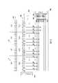
以下請參照圖3,圖3繪示對應本發明圖2實施例的記憶體內運算器的實施方式的示意圖。記憶體內運算器300包括記憶胞陣列310、感測放大器320、輸入緩衝器330以及字元線驅動器340。在圖3中,輸入信號A1~An皆具有三個位元A1(0)~An(2),並被儲存在輸入緩衝器330中。其中,輸入信號A1~An的第一位元A1(0)~An(0)對應至時間點t0;輸入信號A1~An的第二位元A1(1)~An(1)對應至時間點t1;輸入信號A1~An的第三位元A1(2)~An(2)對應至時間點t2。另外,在記憶胞區塊CAj中,權重值W1j~Wnj的每一者均具有四個位元W1j(0)~W1j(3)、…、Wnj(0)~Wnj(3)。因此,記憶胞陣列310中,權重值W1j~Wnj的每一者對應至四條對應位元線。並且,在輸入緩衝器330中的輸入信號A1~An的每一位元A1(0)~An(2)也可被複製為四份,以分別被傳送至對應的四條對應位元線。Please refer to FIG. 3 below. FIG. 3 is a schematic diagram of an implementation of an in-memory arithmetic unit corresponding to the embodiment of FIG. 2 of the present invention. The in-
在本實施方式中,感測放大器320包括多個感測電路SA1~SA4以及CSA1~CSA4、多個第一乘法器321、第二乘法器322、加法器323以及緩衝器324。在本實施例中,感測電路SA1耦接至權重值W1j~Wnj的第四個位元W1j(3)~Wnj(3)的對應位元線;感測電路SA2耦接至權重值W1j~Wnj的第三個位元W1j(2)~Wnj(2)的對應位元線;感測電路SA3耦接至權重值W1j~Wnj的第二個位元W1j(1)~Wnj(1)的對應位元線;感測電路SA4耦接至權重值W1j~Wnj的第一個位元W1j(0)~Wnj(0)的對應位元線。感測電路SA1~SA4可用以感測對應位元線上的電流值或電流放電率。另外,感測電路CSA1~CSA4分別耦接至感測電路SA1~SA4。其中以感測電路CSA1為例,感測電路CSA1用以累加多個感測電路SA1上所感測出的對應位元線上的電流值或電流放電率,來感測出記憶胞區塊CAj所產生的第一運算結果。其中,感測電路CSA1~CSA4可以為類比的電流感測電路。In this embodiment, the
在本實施例中,多個感測電路SA1耦接至相同的第四位元次序的對應位元線;多個感測電路SA2耦接至相同的第三位元次序的對應位元線;多個感測電路SA3耦接至相同的第二位元次序的對應位元線;多個感測電路SA4則耦接至相同的第一位元次序的對應位元線。In this embodiment, the plurality of sensing circuits SA1 are coupled to corresponding bit lines of the same fourth bit order; the plurality of sensing circuits SA2 are coupled to corresponding bit lines of the same third bit order; The plurality of sensing circuits SA3 are coupled to corresponding bit lines of the same second bit order; the plurality of sensing circuits SA4 are coupled to corresponding bit lines of the same first bit order.
第一乘法器321分別耦接至感測電路CSA1~CSA4,並使感測電路CSA1的輸出乘以2的3次方;使感測電路CSA2的輸出乘以2的2次方;以及使感測電路CSA3的輸出乘以2的1次方。第一乘法器321用以產生多個第一信號。第二乘法器322耦接第一乘法器。第二乘法器322使上述的第一信號與2的y次方相乘以產生多個第二信號,其中y依據各輸入信號A1~An的各位元A1(0)~An(2)傳送的時間順序來決定,y為大於或等於0的整數。細節上來說明,在時間點t0時,y=0;在時間點t1時,y=1;在時間點t2時,y=2。第二乘法器322用以產生多個第二信號。The first multiplier 321 is respectively coupled to the sensing circuits CSA1~CSA4, and multiplies the output of the sensing circuit CSA1 by the third power of 2; multiplies the output of the sensing circuit CSA2 by the second power of 2; and makes the sensing The output of the test circuit CSA3 is multiplied by 2 to the power of 1. The first multiplier 321 is used for generating a plurality of first signals. The second multiplier 322 is coupled to the first multiplier. The second multiplier 322 multiplies the above-mentioned first signal by the y power of 2 to generate a plurality of second signals, wherein y is transmitted according to each bit A1(0)~An(2) of each input signal A1~An Time sequence is determined, and y is an integer greater than or equal to 0. In detail, at time t0, y=0; at time t1, y=1; at time t2, y=2. The second multiplier 322 is used to generate a plurality of second signals.
加法器323耦接至第二乘法器322,並用以使多個第二信號相加來產生第二運算結果。在此,第二運算結果也就是記憶體內運算器300的乘加運算結果。The
附帶一提的,緩衝器324可耦接至加法器323,並可作為暫存第二運算結果的媒介。Incidentally, the
以下請參照圖4,圖4繪示本發明另一實施例的記憶體內運算器的示意圖。記憶體內運算器400包括記憶胞陣列410、感測放大器420以及字元線驅動器440。記憶胞陣列410中具有多個記憶胞區塊CAj~CAm。以記憶胞區塊CAj為範例,記憶胞區塊CAj中儲存權重值W1j~Wnj,其中每一權重值W1j~Wnj可具有多個位元。Please refer to FIG. 4 below. FIG. 4 is a schematic diagram of an in-memory arithmetic unit according to another embodiment of the present invention. The in-
在本實施例中,輸入信號A1~An由輸入緩衝器(未繪示)所提供,輸入信號A1~An皆可具有多個位元。其中,輸入緩衝器使各個輸入信號A1~An的多個位元並列的傳送至多條對應位元線上。以各個輸入信號A1~An均具有三個位元為範例,本實施例的輸入緩衝器使輸入信號A1(0)、A1(1)、A1(2)同時被傳送至對應權重值W1j的多條對應位元線上,並同時使輸入信號An(0)、An(1)、An(2)同時被傳送至對應權重值Wnj的多條對應位元線上。In this embodiment, the input signals A1~An are provided by input buffers (not shown), and each of the input signals A1~An can have a plurality of bits. Wherein, the input buffer enables multiple bits of each input signal A1˜An to be transmitted in parallel to multiple corresponding bit lines. Taking each of the input signals A1~An having three bits as an example, the input buffer of this embodiment enables the input signals A1(0), A1(1), and A1(2) to be simultaneously transmitted to the corresponding weight value W1j. corresponding bit lines, and at the same time, the input signals An(0), An(1), An(2) are simultaneously transmitted to a plurality of corresponding bit lines corresponding to the weight values Wnj.
相較於圖2的實施例,本實施例不利用分時傳送輸入信號的多個位元至對應位元線的方式,而是透過並列的傳送輸入信號的多個位元至多條對應位元線上,可有效節省運算時間。而在此實施例中,權重值W1j~Wnj的多個位元可被複製為多份的複製權重值,並使多份的複製權重值寫入至記憶胞區塊CAj。其中,在本實施例中,權重值W1j~Wnj可分別複製成三份的複製權重值。Compared with the embodiment in FIG. 2 , this embodiment does not use the method of time-divisionally transmitting multiple bits of the input signal to corresponding bit lines, but transmits multiple bits of the input signal to multiple corresponding bit lines in parallel. Online, which can effectively save computing time. In this embodiment, multiple bits of the weight values W1j˜Wnj can be copied into multiple copies of the weight values, and the multiple copies of the weight values are written into the memory cell block CAj. Wherein, in this embodiment, the weight values W1j˜Wnj can be copied into three copy weight values respectively.
以下可參照圖5,圖5繪示對應本發明圖4實施例的記憶體內運算器的實施方式的示意圖。記憶體內運算器500包括記憶胞陣列510、感測放大器520、輸入緩衝器530以及字元線驅動器540。在本實施方式中,輸入緩衝器530可使輸入信號A1、A2的多個位元A1(2)~A1(0)、A2(2)並列的被傳送至多條對應位元線上。Referring to FIG. 5 , FIG. 5 is a schematic diagram of an implementation of an in-memory arithmetic unit corresponding to the embodiment of FIG. 4 of the present invention. The in-
記憶胞陣列510中的記憶胞區塊CAj用以儲存權重值W1j~W2j的多個位元W1j(0)~W1j(3)、…、W2j(0)~W2j(3)。在本實施方式中,以輸入信號A1為例,對應於輸入信號A1的多個位元A1(2)~A1(0),權重值W1j可以複製為三份(對應具有三個位元的輸入信號A1),並被儲存在記憶胞區塊CAj中。The memory cell block CAj in the
在本實施方式中,輸入信號A1~A2的所有位元A1(2)~A1(0)、A2(2)可以一次性的被輸入至記憶胞區塊CAj中以執行乘法運算。In this embodiment, all the bits A1(2)-A1(0), A2(2) of the input signals A1-A2 can be input into the memory cell block CAj at one time to perform multiplication.
另外,感測放大器520包括多個感測電路SA1~SA6、CSA1~CSA6、乘法器521以及加法器522。感測電路SA1~SA6分別耦接至不同位元次序的對應位元線,並用以感測對應位元線上的電流值或電流放電率。感測電路CSA1~CSA6分別耦接至感測電路SA1~SA6。其中以感測電路CSA1為例,感測電路CSA1用以累加多個感測電路SA1上所感測出的對應位元線上的電流值或電流放電率,來感測出記憶胞區塊CAj所產生的第一運算結果。其中,感測電路CSA1~CSA6可以為類比的電流感測電路。In addition, the
乘法器521分別耦接至感測電路CSA1~CSA5的輸出端。並使感測電路CSA1的輸出乘以2的5次方;使感測電路CSA2的輸出乘以2的4次方;使感測電路CSA3的輸出乘以2的3次方;使感測電路CSA4的輸出乘以2的2次方;並使感測電路CSA5的輸出乘以2的1次方。乘法器521用以產生多個第一信號。The
加法器522則耦接第一乘法器521。加法器522使第一乘法器521所產生的第一信號相加以產生第二運算結果。The
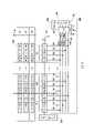
以下請參照圖6,圖6繪示本發明另一實施例的記憶體內運算器的示意圖。記憶體內運算器600包括記憶胞陣列610、感測放大器620以及字元線驅動器640。記憶胞陣列610中具有多個記憶胞區塊CAj~CAm。與圖4實施例不相同的,在本實施例中,記憶胞區塊CAj所儲存的權重值W1j~Wnj是依據權重值W1j~Wnj的每一位元的位元次序來進行排列的。在細節上,以權重值W1j為例,被複製的相同權重值W1j具有多個權重值W1j位元W1j(0)~W1j(3)。多個權重值W1j位元W1j(0)被儲存在相鄰的多條第一對應位元線;多個權重值W1j位元W1j(1)被儲存在相鄰的多條第二對應位元線;多個權重值W1j位元W1j(2)被儲存在相鄰的多條第三對應位元線;多個權重值W1j位元W1j(3)則被儲存在相鄰的多條第四對應位元線。Please refer to FIG. 6 below. FIG. 6 is a schematic diagram of an in-memory arithmetic unit according to another embodiment of the present invention. The in-
在實施細節上,可參照圖7繪示的對應本發明圖6實施例的記憶體內運算器的一實施方式的示意圖。記憶體內運算器700包括記憶胞陣列710、感測放大器720、輸入緩衝器730以及字元線驅動器740。記憶胞陣列710中具有記憶胞區塊CAj。記憶胞區塊CAj中,相鄰的對應位元線的記憶胞用以儲存相同位元次序的權重值W1j的多個位元。在本實施例中,多條位元線BL3上的記憶胞均儲存權重值W1j的位元W1j(3);多條位元線BL2上的記憶胞均儲存權重值W1j的位元W1j(2);多條位元線BL1上的記憶胞均儲存權重值W1j的位元W1j(1);多條位元線BL0上的記憶胞均儲存權重值W1j的位元W1j(0)。For implementation details, reference may be made to FIG. 7 , which is a schematic diagram of an implementation of the in-memory computing unit corresponding to the embodiment of FIG. 6 of the present invention. The in-
輸入緩衝器730則提供輸入信號A1~A2至記憶胞區塊CAj。在細節上,以輸入信號A1為範例,輸入緩衝器730可儲存複製為多份的輸入信號A1,並依據每一份的輸入信號A1的位元高低順序,將輸入信號A1的多個位元A1(3)~A1(0)提供至對應位元線BL3;將輸入信號A1的多個位元A1(3)~A1(0)提供至對應位元線BL2;將輸入信號A1的多個位元A1(3)~A1(0)提供至對應位元線BL1;將輸入信號A1的多個位元A1(3)~A1(0)提供至對應位元線BL0。The
感測放大器720包括感測電路SA1~SA6、CSA1~CSA6、乘法器721以及加法器722。感測電路SA1~SA6用以感測對應位元線上的電流值或電流放電率。在本實施例中,感測電路SA1~SA6的輸出端分別耦接至感測電路CSA1~CSA6。感測電路CSA1~CSA6用以分別累加多個感測電路SA1~SA6上所感測出的對應位元線上的電流值或電流放電率,來感測出記憶胞區塊CAj所產生的第一運算結果。其中,感測電路CSA1~CSA6可以為類比的電流感測電路。The
乘法器721耦接至感測電路CSA1~CSA5的輸出端,並使感測電路CSA1的輸出乘以2的5次方;使感測電路CSA2的輸出乘以2的4次方;使感測電路CSA3的輸出乘以2的3次方;使感測電路CSA4的輸出乘以2的2次方;使感測電路CSA5的輸出乘以2的1次方。乘法器721用以產生多個第一信號。加法器722耦接乘法器721,並用以使多個第一信號相加來產生第二運算結果。在此,第二運算結果也就是記憶體內運算器700的乘加運算結果。The
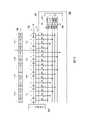
接著請參照圖8,圖8繪示本發明另一實施例的記憶體內運算器的示意圖。記憶體內運算器800包括記憶胞陣列810、感測放大器820以及字元線驅動器840。記憶胞陣列810中具有記憶胞區塊CAj~CAm。以記憶胞區塊CAj為例,記憶胞區塊CAj以及輸入緩衝器(未繪示)可依據乘法運算時所產生的第一運算結果的位元次序,來設定權重值的多個位元Wij(0)~Wij(3)以及與輸入信號的多個位元Ai(0)~Ai(2)間的對應排列關係。在細節上,輸入信號的位元Ai(2)與權重值的位元Wij(3)相乘,可產生第一運算結果的最高有效位元,因此相對應被設定在25的欄位中。輸入信號的位元Ai(1)與權重值的位元Wij(3)相乘,以及輸入信號的位元Ai(2)與權重值的位元Wij(2)相乘,均可產生第一運算結果的第二高位元,因此相對應被設定在24的欄位中。而輸入信號的位元Ai(0)與權重值的位元Wij(0)相乘,則可產生第一運算結果的最低有效位元,因此相對應被設定在20的欄位中。其餘欄位(24~21)的設定方式可依上述原則進行類推。Next, please refer to FIG. 8 . FIG. 8 is a schematic diagram of an in-memory arithmetic unit according to another embodiment of the present invention. The in-
以下參照圖9,圖9繪示對應本發明圖8實施例的記憶體內運算器的一實施方式的示意圖。記憶體內運算器900包括記憶胞陣列910、感測放大器920、輸入緩衝器930以及字元線驅動器940。記憶胞陣列910中具有記憶胞區塊CAj,其中在第一個欄位F1中,記憶胞區塊CAj儲存權重值的最高有效位元Wij(3)。相對應的,輸入緩衝器930在第一個欄位F1中則提供輸入信號的最高有效位元Ai(2)。在第二個欄位F2中,記憶胞區塊CAj儲存權重值的最高有效位元Wij(3)以及第二高位元Wij(2)。相對應的,輸入緩衝器930在第二個欄位F2中則提供輸入信號的位元Ai(1)以及Ai(2)。其中,輸入信號的位元Ai(1)以及Ai(2)分別對應權重值的位元Wij(3)以及Wij(2)。Referring to FIG. 9 below, FIG. 9 is a schematic diagram of an implementation of an in-memory computing unit corresponding to the embodiment of FIG. 8 of the present invention. The in-
在第一欄位F1中,輸入信號的位元Ai(2)與權重值的位元Wij(3)的乘法結果,可產生第一運算結果的最高有效位元。在第二欄位F2中,輸入信號的位元Ai(1)與權重值的位元Wij(3)的乘法結果以及輸入信號的位元Ai(2)與權重值的位元Wij(2)的乘法結果,則可產生第一運算結果的第二高有效位元,其餘欄位則可依此類推。In the first field F1, the multiplication result of the bit Ai(2) of the input signal and the bit Wij(3) of the weight value can generate the most significant bit of the first operation result. In the second field F2, the multiplication result of bit Ai(1) of the input signal and bit Wij(3) of the weight value and bit Ai(2) of the input signal and bit Wij(2) of the weight value The multiplication result of , then the second most significant bit of the first operation result can be generated, and the rest of the fields can be deduced by analogy.
感測放大器920包括感測電路SA1~SA3、CSA1~CSA6、乘法器921以及加法器922。感測電路SA1均設置在第一欄位F1中,感測電路SA2均設置在第二欄位F2中,其餘可依此類推。感測電路SA1~SA3用以感測對應位元線上的電流值或電流放電率。感測電路CSA1~CSA6用以分別累加多個感測電路SA1~SA3上所感測出的對應位元線上的電流值或電流放電率,來感測出記憶胞區塊CAj所產生的第一運算結果。乘法器921耦接至感測電路CSA1~CSA5的輸出端,並使感測電路CSA1的輸出乘以2的5次方;使感測電路CSA2的輸出乘以2的4次方;使感測電路CSA3的輸出乘以2的3次方;使感測電路CSA4的輸出乘以2的2次方;使感測電路CSA5的輸出乘以2的1次方。乘法器921用以產生多個第一信號。加法器922耦接乘法器921,並用以使多個第一信號相加來產生第二運算結果。在此,第二運算結果也就是記憶體內運算器900的乘加運算結果。The
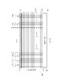
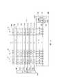
請參照圖10,圖10繪示本發明另一實施例的記憶體內運算器的示意圖。記憶體內運算器1000包括記憶胞陣列1010、感測放大器1020以及字元線驅動器1040。記憶胞陣列1010中具有記憶胞區塊CAj~CAm。以記憶胞區塊CAj為例,記憶胞區塊CAj具有多個記憶列以分別對應多條字元線。字元線驅動器1040可依序啟動這些字元線。記憶胞區塊CAj用以儲存權重值的多個位元,權重值的多個位元的排列方式可在下述的實施方式中具體說明。Please refer to FIG. 10 , which is a schematic diagram of an in-memory arithmetic unit according to another embodiment of the present invention. The in-
輸入緩衝器(未繪示)用以提供輸入信號A1~An的多個位元至記憶胞區塊CAj的多條對應位元線上。記憶胞區塊CAj則可依據依序被開啟的位元線,來使權重值的多個位元與輸入信號A1~An的多個位元進行乘法運算,並產生第一運算結果。The input buffer (not shown) is used to provide a plurality of bits of the input signals A1˜An to a plurality of corresponding bit lines of the memory cell block CAj. The memory cell block CAj can perform a multiplication operation on multiple bits of the weight value and multiple bits of the input signals A1˜An according to the sequentially turned on bit lines, and generate a first operation result.
感測放大器1020用以感測第一運算結果,並使第一運算結果依據位元次序來執行加法運算,可產生第二運算結果。The
接著請參照圖11,圖11繪示對應本發明圖10實施例的記憶體內運算器的實施方式的示意圖。記憶體內運算器1100包括記憶胞陣列1110、感測放大器1120、輸入緩衝器1130以及字元線驅動器1140。記憶胞陣列1110中具有記憶胞區塊CAj。記憶胞區塊CAj對應字元線WL1~WL6。記憶胞區塊CAj可區分為多個欄位F1~Fn,每一欄位儲存權重值W1j~Wnj的多個位元W1j(0)~W1j(3)、…、Wnj(0)~Wnj(3)。而多個欄位F1~Fn分別對應接收輸入信號A1~An的多個位元A1(2)~A1(0)、…、An(2)~An(0)。Next, please refer to FIG. 11 . FIG. 11 is a schematic diagram of an implementation of an in-memory arithmetic unit corresponding to the embodiment of FIG. 10 of the present invention. The in-
舉例來說明,在欄位F1中,對應字元線WL1的記憶列中,記憶胞區塊CAj儲存權重值的一個位元W1j(0);對應字元線WL2的記憶列中,記憶胞區塊CAj則依序儲存權重值的兩個位元W1j(1)、W1j(0);對應字元線WL3的記憶列中,記憶胞區塊CAj則依序儲存權重值的兩個位元W1j(2)、W1j(1)、W1j(0);對應字元線WL4的記憶列中,記憶胞區塊CAj則依序儲存權重值的兩個位元W1j(3)、W1j(2)、W1j(1);對應字元線WL5的記憶列中,記憶胞區塊CAj則依序儲存權重值的兩個位元W1j(3)、W1j(2);對應字元線WL6的記憶列中,記憶胞區塊CAj則儲存權重值的兩個位元W1j(3)。在記憶胞區塊CAj中,未儲存權重值的記憶胞則儲存0。For example, in the field F1, in the memory row corresponding to the word line WL1, the memory cell block CAj stores a bit W1j(0) of the weight value; in the memory row corresponding to the word line WL2, the memory cell block CAj The block CAj sequentially stores the two bits W1j(1) and W1j(0) of the weight value; in the memory column corresponding to the word line WL3, the memory cell block CAj sequentially stores the two bits W1j of the weight value (2), W1j(1), W1j(0); in the memory row corresponding to the word line WL4, the memory cell block CAj sequentially stores two bits W1j(3), W1j(2), W1j(1); in the memory column corresponding to the word line WL5, the memory cell block CAj sequentially stores two bits W1j(3) and W1j(2) of the weight value; in the memory column corresponding to the word line WL6 , and the memory cell block CAj stores two bits W1j(3) of the weight value. In the memory cell block CAj, memory cells that do not store weight values
由上述的說明可以得知,在相同的欄位F1~Fn中,記憶胞區塊CAj在每一字元線WL1~WL6上,可儲存一個或一個以上的權重值的位元W1j(3)~W1j(0)。而權重值的位元W1j(3)~W1j(0)的排列方式,則與對應的輸入信號(以輸入信號A1為例)的位元A1(2)~A1(0)相乘後所產生的運算結果的位元次序相關聯。It can be seen from the above description that in the same fields F1~Fn, the memory cell block CAj can store one or more bits W1j(3) of weight value on each word line WL1~WL6 ~W1j(0). The arrangement of the bits W1j(3)~W1j(0) of the weight value is generated by multiplying the bits A1(2)~A1(0) of the corresponding input signal (take the input signal A1 as an example). The bit order of the operation result is associated.
感測放大器1120包括感測電路SA1以及CSA1。感測電路SA1用以感測對應位元線上的電流值或電流放電率。感測電路CSA1用以累加多個感測電路SA1上所感測出的對應位元線上的電流值或電流放電率,來感測出記憶胞區塊CAj所產生的第一運算結果。The
在此請注意,由於字元線WL1~WL6是分時被啟動的,且基於本實施例的權重值的特殊排列方式,在相同的時間點上,所有感測電路SA1所感測出的對應位元線上的電流值或電流放電率皆對應相同位元次序。Please note here that since the word lines WL1~WL6 are activated in time division, and based on the special arrangement of the weight values in this embodiment, at the same time point, the corresponding bits sensed by all the sensing circuits SA1 The current value or current discharge rate on the element line corresponds to the same bit sequence.
乘法器1121可依據字元線WL1~WL6的開啟順序,使感測電路CSA1的輸出與2的冪次方y相乘,以獲得多個第一信號。其中,在本實施方式中,當字元線WL1~WL6依序被開啟時,y可以依序等於0~5。The
加法器1122耦接乘法器1121,並用以使多個第一信號相加來產生第二運算結果。在此,第二運算結果也就是記憶體內運算器1100的乘加運算結果。The
請參照圖12,圖12繪示本發明實施例的記憶體內運算方法的流程圖。其中,在步驟S1210中,在記憶胞陣列中,提供對應至少一字元線的記憶胞區塊,使記憶胞區塊儲存多個權重值,其中記憶胞區塊上的多個記憶胞儲存對應的各權重值的多個位元。在步驟S1220中,提供輸入緩衝器以分別傳送多個輸入信號至該些位元線。在步驟S1230中,使輸入信號與權重值在記憶胞陣列中進行乘法運算以產生分別對應多個位元次序的多個第一運算結果。以及,在步驟S1240中,依據第一運算結果對應的位元次序,使第一運算結果相加以產生第二運算結果。Please refer to FIG. 12 . FIG. 12 is a flow chart of an in-memory computing method according to an embodiment of the present invention. Wherein, in step S1210, in the memory cell array, a memory cell block corresponding to at least one word line is provided, so that the memory cell block stores a plurality of weight values, wherein a plurality of memory cell blocks on the memory cell block store corresponding Multiple bits for each weight value of . In step S1220, an input buffer is provided to respectively transmit a plurality of input signals to the bit lines. In step S1230, the input signal and the weight value are multiplied in the memory cell array to generate a plurality of first operation results respectively corresponding to a plurality of bit sequences. And, in step S1240, according to the bit sequence corresponding to the first operation result, the first operation results are added to generate the second operation result.
關於上述步驟的實施細節,在前述的實施例中已有詳細的說明,在此恕不多贅述。The implementation details of the above steps have been described in detail in the aforementioned embodiments, and will not be repeated here.
綜上所述,本發明的記憶體內運算器透過使記憶胞區塊中所儲存的權重值的多個位元與輸入信號的多個位元間,利用分時及/或空間配置上的對應關係,可以達到權重值的多個位元與輸入信號的多個位元間以兩兩相乘的方式進行運算。如此一來,記憶體內運算器的硬體結構可以被簡單化。並使利用單階儲存記憶胞形式的反及式快閃記憶體,可以用以實施本發明的記憶體內運算器。To sum up, the intra-memory arithmetic unit of the present invention makes use of time-sharing and/or spatial configuration correspondence between the multiple bits of the weight value stored in the memory cell block and the multiple bits of the input signal. The relationship between multiple bits of the weight value and multiple bits of the input signal can be multiplied in pairs. In this way, the hardware structure of the in-memory arithmetic unit can be simplified. And the NAND-type flash memory using single-level storage memory cells can be used to implement the in-memory arithmetic unit of the present invention.
100、200、300、400、500、600、700、800、900、1000、1100:記憶體內運算器 110、210、310、410、510、610、710、810、910、1010、1110:記憶胞陣列 120、220、320、420、520、620、720、820、920、1020、1120:感測放大器 130、230、330、530、730、930、1130:輸入緩衝器 140、240、340、440、540、640、740、840、940、1040、1140:字元線驅動器 A:輸入信號組 A1~An:輸入信號 CA1~CAm:記憶胞區塊 W:權重值組 W1j~Wnj:權重值 A1(0)~An(2)、A1(p-1)~An(p-1)、W1j(0)~Wnj(3)、Ai(1)、Ai(2):位元 t1~tp-1:時間點 SA1~SA6、CSA1~CSA6:感測電路 321、322、521、721、921、1121:乘法器 323、522、722、922、1122:加法器 324:緩衝器 F1、F2:欄位100, 200, 300, 400, 500, 600, 700, 800, 900, 1000, 1100: In-
圖1繪示本發明一實施例的記憶體內運算器的示意圖。 圖2繪示本發明另一實施例的記憶體內運算器的示意圖。 圖3繪示對應本發明圖2實施例的記憶體內運算器的實施方式的示意圖。 圖4繪示本發明另一實施例的記憶體內運算器的示意圖。 圖5繪示對應本發明圖4實施例的記憶體內運算器的實施方式的示意圖。 圖6繪示本發明另一實施例的記憶體內運算器的示意圖。 圖7繪示對應本發明圖6實施例的記憶體內運算器的一實施方式的示意圖。 圖8繪示本發明另一實施例的記憶體內運算器的示意圖。 圖9繪示對應本發明圖8實施例的記憶體內運算器的一實施方式的示意圖。 圖10繪示本發明另一實施例的記憶體內運算器的示意圖。 圖11繪示對應本發明圖10實施例的記憶體內運算器的實施方式的示意圖。 圖12繪示本發明實施例的記憶體內運算方法的流程圖。FIG. 1 is a schematic diagram of an in-memory arithmetic unit according to an embodiment of the present invention. FIG. 2 is a schematic diagram of an in-memory arithmetic unit according to another embodiment of the present invention. FIG. 3 is a schematic diagram of an implementation of an in-memory arithmetic unit corresponding to the embodiment of FIG. 2 of the present invention. FIG. 4 is a schematic diagram of an in-memory arithmetic unit according to another embodiment of the present invention. FIG. 5 is a schematic diagram of an implementation of an in-memory arithmetic unit corresponding to the embodiment of FIG. 4 of the present invention. FIG. 6 is a schematic diagram of an in-memory arithmetic unit according to another embodiment of the present invention. FIG. 7 is a schematic diagram of an implementation of an in-memory arithmetic unit corresponding to the embodiment of FIG. 6 of the present invention. FIG. 8 is a schematic diagram of an in-memory arithmetic unit according to another embodiment of the present invention. FIG. 9 is a schematic diagram of an implementation of an in-memory arithmetic unit corresponding to the embodiment of FIG. 8 of the present invention. FIG. 10 is a schematic diagram of an in-memory arithmetic unit according to another embodiment of the present invention. FIG. 11 is a schematic diagram of an implementation of an in-memory arithmetic unit corresponding to the embodiment of FIG. 10 of the present invention. FIG. 12 is a flow chart of an in-memory computing method according to an embodiment of the present invention.
100:記憶體內運算器 110:記憶胞陣列 120:感測放大器 130:輸入緩衝器 140:字元線驅動器 A:輸入信號組 A1~An:輸入信號 CA1~CAm:記憶胞區塊 W:權重值組 W1j~Wnj:權重值100: In-memory arithmetic unit 110: memory cell array 120: Sense amplifier 130: Input buffer 140: word line driver A: input signal group A1~An: input signal CA1~CAm: memory cell block W: weight value group W1j~Wnj: weight value
Claims (20)
Translated fromChineseApplications Claiming Priority (2)
| Application Number | Priority Date | Filing Date | Title |
|---|---|---|---|
| US202163142976P | 2021-01-28 | 2021-01-28 | |
| US63/142,976 | 2021-01-28 |
Publications (2)
| Publication Number | Publication Date |
|---|---|
| TW202230367A TW202230367A (en) | 2022-08-01 |
| TWI782573Btrue TWI782573B (en) | 2022-11-01 |
Family
ID=82495774
Family Applications (1)
| Application Number | Title | Priority Date | Filing Date |
|---|---|---|---|
| TW110121220ATWI782573B (en) | 2021-01-28 | 2021-06-10 | In-memory computation device and in-memory computation method |
Country Status (3)
| Country | Link |
|---|---|
| US (2) | US11664070B2 (en) |
| CN (1) | CN114816326B (en) |
| TW (1) | TWI782573B (en) |
Families Citing this family (9)
| Publication number | Priority date | Publication date | Assignee | Title |
|---|---|---|---|---|
| TWI782573B (en)* | 2021-01-28 | 2022-11-01 | 旺宏電子股份有限公司 | In-memory computation device and in-memory computation method |
| US11657864B1 (en)* | 2021-12-17 | 2023-05-23 | Winbond Electronics Corp. | In-memory computing apparatus and computing method having a memory array includes a shifted weight storage, shift information storage and shift restoration circuit to restore a weigh shifted amount of shifted sum-of-products to generate multiple restored sum-of-products |
| KR20240080913A (en)* | 2022-11-30 | 2024-06-07 | 에스케이하이닉스 주식회사 | Storage device and operating method thereof |
| US12190941B2 (en) | 2022-12-28 | 2025-01-07 | Macronix International Co., Ltd. | Memory cell and memory device thereof |
| US12347481B2 (en) | 2023-01-16 | 2025-07-01 | Macronix International Co., Ltd. | Universal memory for in-memory computing and operation method thereof |
| TWI856602B (en)* | 2023-01-16 | 2024-09-21 | 旺宏電子股份有限公司 | Universal memory for in-memory computing and operation method thereof |
| IT202300011370A1 (en)* | 2023-06-05 | 2024-12-05 | St Microelectronics Int Nv | MEMORY COMPUTING DEVICE FOR PERFORMING A SIGNED MAC OPERATION |
| EP4474977B1 (en)* | 2023-06-05 | 2025-10-01 | STMicroelectronics International N.V. | In-memory computation device for performing a multiply-and-accumulate (mac) operation, having a low elaboration time |
| US20250218475A1 (en)* | 2024-01-03 | 2025-07-03 | Qualcomm Incorporated | Compute-in-Memory with Current Transition Detection |
Citations (4)
| Publication number | Priority date | Publication date | Assignee | Title |
|---|---|---|---|---|
| US20170277659A1 (en)* | 2016-03-23 | 2017-09-28 | Gsi Technology Inc. | In memory matrix multiplication and its usage in neural networks |
| WO2020159800A1 (en)* | 2019-01-28 | 2020-08-06 | Rambus Inc. | Memory-integrated neural network |
| TWI705391B (en)* | 2018-05-29 | 2020-09-21 | 英屬開曼群島商意騰科技股份有限公司 | In-memory computing memory device and in-memory computing memory block for use in artificial neuron |
| US20200311523A1 (en)* | 2019-03-28 | 2020-10-01 | Sandisk Technologies Llc | Realization of neural networks with ternary inputs and binary weights in nand memory arrays |
Family Cites Families (11)
| Publication number | Priority date | Publication date | Assignee | Title |
|---|---|---|---|---|
| US5014235A (en)* | 1987-12-15 | 1991-05-07 | Steven G. Morton | Convolution memory |
| US6096604A (en)* | 1999-08-04 | 2000-08-01 | Chartered Semiconductor Manufacturing Ltd | Production of reversed flash memory device |
| US9111224B2 (en)* | 2011-10-19 | 2015-08-18 | Qualcomm Incorporated | Method and apparatus for neural learning of natural multi-spike trains in spiking neural networks |
| CN103176767B (en)* | 2013-03-01 | 2016-08-03 | 浙江大学 | The implementation method of the floating number multiply-accumulate unit that a kind of low-power consumption height is handled up |
| KR102408858B1 (en)* | 2017-12-19 | 2022-06-14 | 삼성전자주식회사 | A nonvolatile memory device, a memory system including the same and a method of operating a nonvolatile memory device |
| US10817260B1 (en)* | 2018-06-13 | 2020-10-27 | Amazon Technologies, Inc. | Reducing dynamic power consumption in arrays |
| US12008460B2 (en)* | 2019-09-05 | 2024-06-11 | Micron Technology, Inc. | Performing processing-in-memory operations related to pre-synaptic spike signals, and related methods and systems |
| CN112101539B (en)* | 2020-11-18 | 2021-07-20 | 南京优存科技有限公司 | A storage-computing integrated circuit and artificial intelligence chip |
| TWI782573B (en)* | 2021-01-28 | 2022-11-01 | 旺宏電子股份有限公司 | In-memory computation device and in-memory computation method |
| US11935586B2 (en)* | 2022-02-11 | 2024-03-19 | Taiwan Semiconductor Manufacturing Company, Ltd. | Memory device and method for computing-in-memory (CIM) |
| US20240303037A1 (en)* | 2023-03-09 | 2024-09-12 | Micron Technology, Inc. | Memory device having bonded integrated circuit dies used for multiplication |
- 2021
- 2021-06-10TWTW110121220Apatent/TWI782573B/enactive
- 2021-06-10USUS17/344,555patent/US11664070B2/enactiveActive
- 2021-06-23CNCN202110695913.XApatent/CN114816326B/enactiveActive
- 2023
- 2023-04-19USUS18/303,194patent/US12362003B2/enactiveActive
Patent Citations (4)
| Publication number | Priority date | Publication date | Assignee | Title |
|---|---|---|---|---|
| US20170277659A1 (en)* | 2016-03-23 | 2017-09-28 | Gsi Technology Inc. | In memory matrix multiplication and its usage in neural networks |
| TWI705391B (en)* | 2018-05-29 | 2020-09-21 | 英屬開曼群島商意騰科技股份有限公司 | In-memory computing memory device and in-memory computing memory block for use in artificial neuron |
| WO2020159800A1 (en)* | 2019-01-28 | 2020-08-06 | Rambus Inc. | Memory-integrated neural network |
| US20200311523A1 (en)* | 2019-03-28 | 2020-10-01 | Sandisk Technologies Llc | Realization of neural networks with ternary inputs and binary weights in nand memory arrays |
Also Published As
| Publication number | Publication date |
|---|---|
| US12362003B2 (en) | 2025-07-15 |
| US20230253032A1 (en) | 2023-08-10 |
| CN114816326B (en) | 2025-09-05 |
| US20220238151A1 (en) | 2022-07-28 |
| CN114816326A (en) | 2022-07-29 |
| US11664070B2 (en) | 2023-05-30 |
| TW202230367A (en) | 2022-08-01 |
Similar Documents
| Publication | Publication Date | Title |
|---|---|---|
| TWI782573B (en) | In-memory computation device and in-memory computation method | |
| CN113419705B (en) | In-memory multiplication and addition computing circuit, chip, and computing device | |
| KR20200082617A (en) | Calculation method using memory device and memory device performing the same | |
| US20220188604A1 (en) | Method and Apparatus for Performing a Neural Network Operation | |
| CN113885831B (en) | Storage and computing integrated circuit, chip and computing device based on mixed data input | |
| TWI784879B (en) | Computing method and electronic device | |
| CN115148234A (en) | Computing in Memory (CIM) Storage Arrays | |
| CN113268220B (en) | Memory Multiplication Circuit Based on Time Domain and Memory Multiplication and Addition Circuit Based on Time Domain | |
| KR20220008743A (en) | In-memory computation circuit and method | |
| CN115495152A (en) | Memory computing circuit with variable length input | |
| TWI842375B (en) | Method for reading memory and memory device | |
| KR20220054664A (en) | Methods and systems for performing in-memory processing operations related to pre-synaptic spike signals | |
| US12373131B2 (en) | Data sequencing circuit and method | |
| CN113838497B (en) | A simplified storage and computing circuit that can be used for data reading | |
| US12032959B2 (en) | Non-volatile memory die with latch-based multiply-accumulate components | |
| CN112862059B (en) | Long short-term memory (LSTM) network computing device and computing device | |
| CN119229916A (en) | Dual-port storage and computing integrated circuit, chip and electronic device | |
| TWI851495B (en) | Page buffer circuit and operating method thereof adapted for page read device | |
| US20240385802A1 (en) | System and methods for performing mac operations on floating point numbers | |
| US20250094125A1 (en) | Multi-mode compute-in-memory systems and methods for operating the same | |
| US20250251911A1 (en) | Systems and methods for post-multiplication alignment for floating point computing-in-memory (cim) | |
| US20250199765A1 (en) | Systems and methods for performing mac operations with reduced computation resources | |
| CN217933180U (en) | Memory computing circuit | |
| US20250191621A1 (en) | Page buffer circuit and operating method thereof adapted for page read device | |
| CN118626049A (en) | In-memory computing circuit and method for performing multiply-accumulate operations |