TWI782401B - Light emitting array structure and display - Google Patents
Light emitting array structure and displayDownload PDFInfo
- Publication number
- TWI782401B TWI782401BTW110102882ATW110102882ATWI782401BTW I782401 BTWI782401 BTW I782401BTW 110102882 ATW110102882 ATW 110102882ATW 110102882 ATW110102882 ATW 110102882ATW I782401 BTWI782401 BTW I782401B
- Authority
- TW
- Taiwan
- Prior art keywords
- layer
- light emitting
- array structure
- light
- substrate
- Prior art date
Links
Images


Classifications
- H—ELECTRICITY
- H01—ELECTRIC ELEMENTS
- H01L—SEMICONDUCTOR DEVICES NOT COVERED BY CLASS H10
- H01L25/00—Assemblies consisting of a plurality of semiconductor or other solid state devices
- H01L25/16—Assemblies consisting of a plurality of semiconductor or other solid state devices the devices being of types provided for in two or more different subclasses of H10B, H10D, H10F, H10H, H10K or H10N, e.g. forming hybrid circuits
- H01L25/167—Assemblies consisting of a plurality of semiconductor or other solid state devices the devices being of types provided for in two or more different subclasses of H10B, H10D, H10F, H10H, H10K or H10N, e.g. forming hybrid circuits comprising optoelectronic devices, e.g. LED, photodiodes
- H—ELECTRICITY
- H01—ELECTRIC ELEMENTS
- H01L—SEMICONDUCTOR DEVICES NOT COVERED BY CLASS H10
- H01L25/00—Assemblies consisting of a plurality of semiconductor or other solid state devices
- H01L25/03—Assemblies consisting of a plurality of semiconductor or other solid state devices all the devices being of a type provided for in a single subclass of subclasses H10B, H10D, H10F, H10H, H10K or H10N, e.g. assemblies of rectifier diodes
- H01L25/04—Assemblies consisting of a plurality of semiconductor or other solid state devices all the devices being of a type provided for in a single subclass of subclasses H10B, H10D, H10F, H10H, H10K or H10N, e.g. assemblies of rectifier diodes the devices not having separate containers
- H01L25/075—Assemblies consisting of a plurality of semiconductor or other solid state devices all the devices being of a type provided for in a single subclass of subclasses H10B, H10D, H10F, H10H, H10K or H10N, e.g. assemblies of rectifier diodes the devices not having separate containers the devices being of a type provided for in group H10H20/00
- H01L25/0753—Assemblies consisting of a plurality of semiconductor or other solid state devices all the devices being of a type provided for in a single subclass of subclasses H10B, H10D, H10F, H10H, H10K or H10N, e.g. assemblies of rectifier diodes the devices not having separate containers the devices being of a type provided for in group H10H20/00 the devices being arranged next to each other
- H—ELECTRICITY
- H10—SEMICONDUCTOR DEVICES; ELECTRIC SOLID-STATE DEVICES NOT OTHERWISE PROVIDED FOR
- H10H—INORGANIC LIGHT-EMITTING SEMICONDUCTOR DEVICES HAVING POTENTIAL BARRIERS
- H10H20/00—Individual inorganic light-emitting semiconductor devices having potential barriers, e.g. light-emitting diodes [LED]
- H10H20/80—Constructional details
- H10H20/85—Packages
- H10H20/855—Optical field-shaping means, e.g. lenses
- H10H20/856—Reflecting means
- H—ELECTRICITY
- H10—SEMICONDUCTOR DEVICES; ELECTRIC SOLID-STATE DEVICES NOT OTHERWISE PROVIDED FOR
- H10H—INORGANIC LIGHT-EMITTING SEMICONDUCTOR DEVICES HAVING POTENTIAL BARRIERS
- H10H20/00—Individual inorganic light-emitting semiconductor devices having potential barriers, e.g. light-emitting diodes [LED]
- H10H20/80—Constructional details
- H10H20/85—Packages
- H10H20/857—Interconnections, e.g. lead-frames, bond wires or solder balls
Landscapes
- Engineering & Computer Science (AREA)
- Microelectronics & Electronic Packaging (AREA)
- Physics & Mathematics (AREA)
- Condensed Matter Physics & Semiconductors (AREA)
- General Physics & Mathematics (AREA)
- Computer Hardware Design (AREA)
- Power Engineering (AREA)
- Led Device Packages (AREA)
- Devices For Indicating Variable Information By Combining Individual Elements (AREA)
- Electroluminescent Light Sources (AREA)
Abstract
Description
Translated fromChinese本揭露是有關於一種發光陣列結構及顯示器。The disclosure relates to a light emitting array structure and a display.
利用巨量轉移(Mass transfer)將微發光二極體(micro-LED)與微晶片(micro-IC)用覆蓋其上的線路重佈(Redistribution Layer, RDL)技術將彼此電性連接,形成顯示畫素陣列,是目前已知之技術。然而,這種結構會有難以修復之缺點。舉例來說,若微發光二極體或微晶片因瑕疵而需要置換,已覆蓋於其上的RDL會使得微發光二極體或微晶片無法取下。即便破壞RDL並置換上新的微發光二極體或微晶片,仍需要針對局部置換區域進行RDL修復,這種工法難以用於以黃光微影製作的RDL,且耗費成本極高。Using mass transfer to electrically connect micro-LEDs and micro-ICs with redistribution layer (RDL) technology covering them to form a display The pixel array is a currently known technology. However, this structure has the disadvantage that it is difficult to repair. For example, if the micro-LED or microchip needs to be replaced due to a defect, the RDL that has covered it will make it impossible to remove the micro-LED or microchip. Even if the RDL is destroyed and replaced with a new micro-LED or microchip, the RDL still needs to be repaired in the local replacement area. This method is difficult to use for RDL produced by yellow light lithography, and the cost is extremely high.
除此之外,因微發光二極體使用巨量轉移的技術進行固晶(bonding)時,難以預先根據微發光二極體的特性進行分規(bining),如此一來,所形成的畫素陣列容易形成顏色不均或亮度不均的狀況。In addition, when micro-light-emitting diodes are bonded using mass transfer technology, it is difficult to perform binning according to the characteristics of micro-light-emitting diodes in advance. Pixel arrays are prone to uneven color or uneven brightness.
有鑑於此,本揭露之一目的在於提出一種可解決上述問題的發光陣列結構。In view of this, one purpose of the present disclosure is to propose a light emitting array structure that can solve the above problems.
為了達到上述目的,本揭露之一態樣是提供一種發光陣列結構,其包含基板、多個發光畫素單元、多條第一訊號線、多條第二訊號線以及封裝層。這些發光畫素單元陣列設置於基板上,且各發光畫素單元包含驅動晶片、第一平坦層、第一重佈線路層、第二平坦層、第二重佈線路層以及發光二極體。驅動晶片設置於基板上。第一平坦層設置於基板上並覆蓋驅動晶片。第一重佈線路層設置於第一平坦層上並電性連接驅動晶片。第二平坦層設置於第一平坦層上並覆蓋第一重佈線路層。第二重佈線路層設置於第二平坦層上並電性連接第一重佈線路層。發光二極體覆晶接觸第二重佈線路層。各第一訊號線電性連接所述第一重佈線路層的對應一者,且各第一訊號線朝第一方向延伸。所述第二訊號線在不同於第一訊號線的水平面上延伸,各第二訊號線電性連接所述第二重佈線路層的對應一者,且各第二訊號線朝不同於第一方向的第二方向延伸。封裝層覆蓋發光畫素單元、第一訊號線、第二訊號線及基板。In order to achieve the above purpose, an aspect of the present disclosure provides a light emitting array structure, which includes a substrate, a plurality of light emitting pixel units, a plurality of first signal lines, a plurality of second signal lines and a packaging layer. These light-emitting pixel unit arrays are arranged on the substrate, and each light-emitting pixel unit includes a driving chip, a first planar layer, a first redistribution circuit layer, a second planar layer, a second redistribution circuit layer and a light emitting diode. The driving chip is arranged on the substrate. The first flat layer is disposed on the substrate and covers the driving chip. The first redistribution circuit layer is disposed on the first planar layer and electrically connected to the driving chip. The second flat layer is disposed on the first flat layer and covers the first redistribution circuit layer. The second redistribution circuit layer is disposed on the second flat layer and electrically connected to the first redistribution circuit layer. The light emitting diode flip-chip contacts the second redistribution circuit layer. Each first signal line is electrically connected to a corresponding one of the first redistribution circuit layers, and each first signal line extends toward a first direction. The second signal lines extend on a horizontal plane different from that of the first signal lines, each second signal line is electrically connected to a corresponding one of the second redistribution wiring layers, and each second signal line faces a direction different from that of the first signal line. The second direction of the direction extends. The encapsulation layer covers the light-emitting pixel unit, the first signal line, the second signal line and the substrate.
根據本揭露一實施方式,所述第一訊號線與所述第一重佈線路層位於同一水平面上。According to an embodiment of the present disclosure, the first signal line and the first redistribution wiring layer are located on the same horizontal plane.
根據本揭露一實施方式,所述第二訊號線與所述第二重佈線路層位於同一水平面上。According to an embodiment of the present disclosure, the second signal line and the second redistribution wiring layer are located on the same horizontal plane.
根據本揭露一實施方式,第一方向實質上垂直於第二方向。According to an embodiment of the present disclosure, the first direction is substantially perpendicular to the second direction.
根據本揭露一實施方式,發光陣列結構更包含一反射層設置於各第二平坦層的頂表面。According to an embodiment of the present disclosure, the light emitting array structure further includes a reflective layer disposed on the top surface of each second flat layer.
根據本揭露一實施方式,反射層包括銀反射鏡、鋁反射鏡或分散式布拉格反射鏡。According to an embodiment of the present disclosure, the reflection layer includes a silver mirror, an aluminum mirror or a distributed Bragg mirror.
根據本揭露一實施方式,各第二重佈線路層的上表面為黑化處理表面。According to an embodiment of the present disclosure, the upper surface of each second redistribution wiring layer is a blackened surface.
根據本揭露一實施方式,所述第一訊號線的上表面為黑化處理表面。According to an embodiment of the present disclosure, the upper surface of the first signal line is a blackened surface.
根據本揭露一實施方式,所述第二訊號線的上表面為黑化處理表面。According to an embodiment of the present disclosure, the upper surface of the second signal line is a blackened surface.
本揭露之另一態樣是提供一種發光陣列結構,其包含基板、驅動晶片、第一平坦層、第一重佈線路層、第二平坦層、第二重佈線路層、多個發光畫素單元、第一訊號線、第二訊號線以及封裝層。驅動晶片設置於基板上。第一平坦層設置於基板上並覆蓋驅動晶片。第一重佈線路層設置於第一平坦層上並電性連接驅動晶片。第二平坦層設置於第一平坦層上並覆蓋第一重佈線路層。第二重佈線路層設置於第二平坦層上並電性連接第一重佈線路層。多個發光畫素單元陣列設置於基板上方。第一訊號線電性連接第一重佈線路層且第一訊號線朝第一方向延伸。第二訊號線在不同於第一訊號線的一水平面上延伸。第二訊號線電性連接第二重佈線路層,且第二訊號線朝不同於第一方向的第二方向延伸。封裝層覆蓋該基板、驅動晶片、第二平坦層、第二重佈線路層、第一訊號線及第二訊號線。Another aspect of the present disclosure is to provide a light-emitting array structure, which includes a substrate, a driving chip, a first planar layer, a first redistribution circuit layer, a second planar layer, a second redistribution circuit layer, and a plurality of light-emitting pixels A unit, a first signal line, a second signal line and a packaging layer. The driving chip is arranged on the substrate. The first flat layer is disposed on the substrate and covers the driving chip. The first redistribution circuit layer is disposed on the first planar layer and electrically connected to the driving chip. The second flat layer is disposed on the first flat layer and covers the first redistribution circuit layer. The second redistribution circuit layer is disposed on the second flat layer and electrically connected to the first redistribution circuit layer. A plurality of light-emitting pixel unit arrays are arranged above the substrate. The first signal line is electrically connected to the first redistribution circuit layer, and the first signal line extends toward the first direction. The second signal line extends on a different horizontal plane than the first signal line. The second signal line is electrically connected to the second redistribution circuit layer, and the second signal line extends in a second direction different from the first direction. The encapsulation layer covers the substrate, the driving chip, the second planar layer, the second redistribution circuit layer, the first signal line and the second signal line.
根據本揭露一實施方式,第一訊號線與第一重佈線路層位於同一水平面上。According to an embodiment of the present disclosure, the first signal line and the first redistribution wiring layer are located on the same horizontal plane.
根據本揭露一實施方式,第二訊號線與第二重佈線路層位於同一水平面上。According to an embodiment of the present disclosure, the second signal line and the second redistribution wiring layer are located on the same horizontal plane.
根據本揭露一實施方式,第一方向實質上垂直於第二方向。According to an embodiment of the present disclosure, the first direction is substantially perpendicular to the second direction.
根據本揭露一實施方式,發光陣列結構更包含一反射層設置於第二平坦層的頂表面。According to an embodiment of the present disclosure, the light emitting array structure further includes a reflective layer disposed on the top surface of the second flat layer.
根據本揭露一實施方式,反射層包括銀反射鏡、鋁反射鏡或分散式布拉格反射鏡。According to an embodiment of the present disclosure, the reflection layer includes a silver mirror, an aluminum mirror or a distributed Bragg mirror.
根據本揭露一實施方式,第二重佈線路層的上表面為黑化處理表面。According to an embodiment of the present disclosure, the upper surface of the second redistribution wiring layer is a blackened surface.
根據本揭露一實施方式,第一訊號線的上表面為黑化處理表面。According to an embodiment of the present disclosure, the upper surface of the first signal line is a blackened surface.
根據本揭露一實施方式,第二訊號線的上表面為黑化處理表面。According to an embodiment of the present disclosure, the upper surface of the second signal line is a blackened surface.
本揭露之又一態樣是提供一種顯示器,其包含驅動基板以及多個如上所述的發光陣列結構。這些發光陣列結構設置於驅動基板上。Another aspect of the present disclosure is to provide a display, which includes a driving substrate and a plurality of light-emitting array structures as described above. These light emitting array structures are arranged on the driving substrate.
為了使本揭露內容的敘述更加詳盡與完備,下文針對了本揭露的實施態樣與具體實施例提出了說明性的描述;但這並非實施或運用本揭露具體實施例的唯一形式。以下所揭露的各實施例,在有益的情形下可相互組合或取代,也可在一實施例中附加其他的實施例,而無須進一步的記載或說明。In order to make the description of the present disclosure more detailed and complete, the following provides an illustrative description of the implementation and specific embodiments of the present disclosure; but this is not the only way to implement or use the specific embodiments of the present disclosure. The various embodiments disclosed below can be combined or replaced with each other when beneficial, and other embodiments can also be added to one embodiment, without further description or illustration.
在以下描述中,將詳細敘述許多特定細節以使讀者能夠充分理解以下的實施例。然而,可在無此等特定細節之情況下實踐本揭露之實施例。在其他情況下,為簡化圖式,熟知的結構與裝置僅示意性地繪示於圖中。In the following description, numerous specific details will be set forth in order to enable readers to fully understand the following embodiments. However, embodiments of the present disclosure may be practiced without these specific details. In other instances, well-known structures and devices are only schematically shown in order to simplify the drawings.
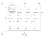
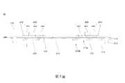
第1圖繪示本揭露一實施方式之發光陣列結構10的上視示意圖。第2圖繪示本揭露一實施方式之發光陣列結構的側視示意圖。請同時參閱第1圖及第2圖,發光陣列結構10包含基板110、多個發光畫素單元120、多條第一訊號線130、多條第二訊號線140以及封裝層150。在多個實施例中,基板110可以為高熱導係數鋁基板、可撓式基板、玻璃基板、金屬複合材料板、陶瓷基板或具有諸如電晶體或積體電路(ICs)之功能元件的半導體基板。FIG. 1 shows a schematic top view of a light
在多個實施例中,基板110還包含導電孔112、第一導電墊114及第二導電墊116。具體的說,導電孔112由基板110的上表面110a貫穿至下表面110b,且第一導電墊114及第二導電墊116分別設置於基板110的上表面110a及下表面110b並接觸導電孔112。在多個實例中,導電孔112的材質例如為銅或其他具導電性的材料,例如銀、鎳、錫或鋁等,但不限於此。在多個實例中,可先利用雷射鑽孔、化學鑽孔、機械鑽孔或其他合適的方式從基板110的上表面110a穿透至下表面110b以形成通孔。接著,在通孔內填入導電材質,以形成導電孔112。在多個實例中,第一導電墊114和第二導電墊116的材質例如可為銅或其他具導電性的材料,例如金、銀、鈀、鎳、錫或鋁等,但不限於此。In various embodiments, the
請繼續參閱第1圖及第2圖。多個發光畫素單元120陣列設置於基板110上。具體的說,各發光畫素單元120包含驅動晶片121、第一平坦層122、第一重佈線路層123、第二平坦層124、第二重佈線路層125以及發光二極體126。更詳細的說,驅動晶片121設置於基板110上。Please continue to refer to Figure 1 and Figure 2. A plurality of light-emitting
在多個實施例中,本揭露所使用的驅動晶片121例如為微型驅動晶片,其尺寸介於約1微米至300微米之間。進一步的說,微型驅動晶片的尺寸例如為10微米、30微米、50微米、70微米、100微米、120微米、150微米、200微米或250微米。可以理解的是,驅動晶片121的電源接腳可連接電源供應電路的輸出端,以接收電源,而驅動晶片121的驅動接腳則連接發光二極體126,以控制發光二極體電路的運作。在多個實施例中,驅動晶片121具有過高溫度保護(over temperature protection,OTP)功能。舉例來說,當驅動晶片121的內部溫度超過預設溫度(例如,100℃)時,會啟動保護功能,例如關閉驅動晶片121以停止接收供應電源。In various embodiments, the
請繼續參閱第1圖及第2圖。更詳細的說,第一平坦層122設置於基板110上並覆蓋驅動晶片121。在多個實施例中,第一平坦層122的材料可以為氧化層或是感光絕緣材料,例如含有環氧樹脂(epoxy)的光阻材料。在多個實施例中,可以利用塗佈、噴塗、印刷或其他合適的方式形成第一平坦層122。Please continue to refer to Figure 1 and Figure 2. In more detail, the first
請繼續參閱第1圖及第2圖。更詳細的說,第一重佈線路層123設置於第一平坦層122上並電性連接驅動晶片121。在一些實施例中,第一重佈線路層123的材料包含銅、鎳、金、鋁、銀或其他合適的金屬。在另一些實施例中,第一重佈線路層123的材料可包含鋁銅、鋁矽銅或其他合金。在一些實施例中,可以利用諸如濺鍍(sputtering)、蒸鍍(evaporating)、電鍍(electroplating)或其他合適的沉積製程、微影製程、和蝕刻製程的方式於第一平坦層122上形成第一重佈線路層123。在另一實施例中,可以先對第一平坦層122的表面進行粗化製程,以使第一重佈線路層123與第一平坦層122之間具有良好結合力。Please continue to refer to Figure 1 and Figure 2. In more detail, the first
請繼續參閱第1圖及第2圖。更詳細的說,第二平坦層124設置於第一平坦層122上並覆蓋第一重佈線路層123。在多個實施例中,第二平坦層124的材料及製作方法可以與第一平坦層122的材料及製作方法相同或類似,在此不再贅述。Please continue to refer to Figure 1 and Figure 2. In more detail, the second
請繼續參閱第1圖及第2圖。更詳細的說,第二重佈線路層125設置於第二平坦層124上並電性連接第一重佈線路層123。在多個實施例中,第二重佈線路層125的材料及製作方法可以與第一重佈線路層123的材料及製作方法相同或類似,在此不再贅述。在多個實施例中,第二重佈線路層125的上表面為一黑化處理表面。這種設計可以增加發光陣列結構10的佔黑比,以避免使用者目視可見。Please continue to refer to Figure 1 and Figure 2. In more detail, the second
請繼續參閱第1圖及第2圖。更詳細的說,發光二極體126覆晶接觸第二重佈線路層125。這種設計,可以使得發光二極體126不會被任何線路覆蓋,因此不影響其出光效率。在多個實施例中,發光二極體126可以為紅色發光二極體、綠色發光二極體、藍色發光二極體、黃色發光二極體、白發光二極體及其組合。在一些實施例中,發光二極體126可以是次毫米發光二極體(mini-LED)或微發光二極體(micro-LED)。雖然第1圖中的每個發光畫素單元120僅包含三個發光二極體126,但發光二極體126的數量可視設計需求增加,例如為4個、5個、6個、7個或者更多。Please continue to refer to Figure 1 and Figure 2. In more detail, the light-emitting
由於本揭露的發光畫素單元120的設計可以使發光二極體126與驅動晶片121位於不同的水平面(level)上,因此,兩者的擺放位置不相互影響。在多個實施例中,發光二極體126的垂直投影與驅動晶片121的垂直投影重疊。這種設計能夠將發光二極體126置中擺放,而不影響發光畫素單元120的出光對稱性並達到更佳的光學效果。在另一實施例中,依照發光設計需求,發光二極體126的垂直投影可以與驅動晶片121的垂直投影不重疊。Since the design of the light-emitting
請繼續參閱第1圖及第2圖。各第一訊號線130電性連接所述第一重佈線路層123的對應一者,且各第一訊號線130朝第一方向D1延伸。在多個實施例中,第一訊號線130的材料可包含鋁銅、鋁矽銅或其他合金。在一些實施例中,可以利用諸如濺鍍(sputtering)、蒸鍍(evaporating)、電鍍(electroplating)或其他合適的沉積製程、微影製程、和蝕刻製程的方式於第一平坦層122上形成第一訊號線130。因此,可以理解的是,這些第一訊號線130與所述第一重佈線路層123位於同一水平面(level)上。在多個實施例中,這些第一訊號線130的上表面為一黑化處理表面。這種設計可以增加發光陣列結構10的佔黑比,以避免使用者目視可見。Please continue to refer to Figure 1 and Figure 2. Each
請繼續參閱第1圖及第2圖。多條第二訊號線140,在不同於所述第一訊號線130的水平面(level)上延伸。更具體的說,各第二訊號線140電性連接所述第二重佈線路層125的對應一者,且各第二訊號線140朝不同於第一方向D1的第二方向D2延伸。在多個實施例中,第二訊號線140的材料可包含鋁銅、鋁矽銅或其他合金。在一些實施例中,可以利用諸如濺鍍(sputtering)、蒸鍍(evaporating)、電鍍(electroplating)或其他合適的沉積製程、微影製程、和蝕刻製程的方式於第二平坦層124上形成第二訊號線140。因此,可以理解的是,在多個實施例中,這些第二訊號線140與所述第二重佈線路層125位於同一水平面(level)上。在多個實施例中,第一方向D1實質上垂直於第二方向D2。在多個實施例中,這些第二訊號線140的一上表面為一黑化處理表面。這種設計可以增加發光陣列結構10的佔黑比,以避免使用者目視可見。Please continue to refer to Figure 1 and Figure 2. A plurality of
請繼續參閱第1圖及第2圖。封裝層150覆蓋所述發光畫素單元120、所述第一訊號線130、所述第二訊號線140及所述基板110。在多個實施例中,封裝層150可包含有機封裝膠材(organic packaging material)、無機封裝膠材(inorganic packaging material)或其組合。舉例來說,有機膠材包含矽橡膠(silicon rubber)、壓克力及環氧樹脂;無機膠材包含矽膠(silicon dioxide)及氟膠,但本揭露不以此為限。在多個實施方式中,可以藉由點膠、封膠(molding)、灌膠(glue-filling)或其他合適的製程來形成封裝層150。封裝層150可以增加屏蔽水氣入侵的面積,保護發光陣列結構10免於受到水氣的干擾,進而提升產品的信賴性及使用壽命。Please continue to refer to Figure 1 and Figure 2. The
在某些實施例中,可進一步增添一添加物(圖未示)於封裝層150中,用以遮蔽線路及增加發光元件的亮度。舉例來說,添加物可以為有機物或無機物的顆粒,例如,陶瓷粒子、金屬粒子、玻璃粒子及高分子粒子等。In some embodiments, an additive (not shown in the figure) can be further added in the
第3圖繪示本揭露另一實施方式之發光陣列結構30的側視示意圖。為了便於比較與上述各實施方式之相異處並簡化說明,在下文之各實施例中使用相同的符號標注相同的元件,且主要針對各實施方式之相異處進行說明,而不再對重覆部分進行贅述。FIG. 3 shows a schematic side view of a light emitting array structure 30 according to another embodiment of the present disclosure. In order to compare the differences with the above-mentioned implementations and simplify the description, the same symbols are used to mark the same components in the following embodiments, and the descriptions are mainly focused on the differences between the implementations, and the repetitions will not be repeated. The overlay part will be repeated.
發光陣列結構30與發光陣列結構10的不同之處在於: 發光陣列結構30還包含一反射層310設置於各第二平坦層124的頂表面。在多個實施例中,反射層310可以為銀反射鏡、鋁反射鏡或分散式布拉格反射鏡(Distributed Bragg Reflector,DBR)。具體的說,分散式布拉格反射鏡可由兩種以上具有不同折射率之同質或異質材料之薄膜相互堆疊所構成。舉例來說,分散式布拉格反射鏡可以由SiO2與TiO2交互堆疊所構成或者由SiO2/Al2O3/TiO2交互堆疊所構成。這種設計可以增加發光陣列結構30之發光效率。The difference between the light emitting array structure 30 and the light emitting
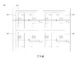
第4圖繪示本揭露一實施方式之發光陣列結構40的上視示意圖。第5圖繪示本揭露一實施方式之發光陣列結構40的剖面示意圖。為了便於比較與上述各實施方式之相異處並簡化說明,在下文之各實施例中使用相同的符號標注相同的元件。請同時參閱第4圖及第5圖,發光陣列結構40包含基板110、驅動晶片410、第一平坦層420、第一重佈線路層430、第二平坦層440、第二重佈線路層450、多個發光畫素單元460、第一訊號線470、第二訊號線480以及封裝層150。FIG. 4 shows a schematic top view of a light emitting
請繼續參閱第4圖及第5圖,驅動晶片410設置於基板110上。在多個實施例中,本揭露所使用的驅動晶片410例如為微型驅動晶片,其尺寸介於約1微米至300微米之間。進一步的說,微型驅動晶片的尺寸例如為10微米、30微米、50微米、70微米、100微米、120微米、150微米、200微米或250微米。可以理解的是,驅動晶片410的電源接腳可連接電源供應電路的輸出端,以接收電源,而驅動晶片410的驅動接腳則連接發光畫素單元460中的發光二極體,以控制發光二極體電路的運作。在多個實施例中,驅動晶片410具有過高溫度保護(over temperature protection,OTP)功能。舉例來說,當驅動晶片410的內部溫度超過預設溫度(例如,100℃)時,會啟動保護功能,例如關閉驅動晶片410以停止接收供應電源。Please continue to refer to FIG. 4 and FIG. 5 , the
請繼續參閱第4圖及第5圖,第一平坦層420設置於基板110上並覆蓋驅動晶片410。在多個實施例中,第一平坦層420的材料可以為氧化層或是感光絕緣材料,例如含有環氧樹脂(epoxy)的光阻材料。在多個實施例中,可以利用塗佈、噴塗、印刷或其他合適的方式形成第一平坦層420。Please continue to refer to FIG. 4 and FIG. 5 , the first
請繼續參閱第4圖及第5圖,第一重佈線路層430設置於第一平坦層420上並電性連接驅動晶片410。在一些實施例中,第一重佈線路層430的材料包含銅、鎳、金、鋁、銀或其他合適的金屬。在另一些實施例中,第一重佈線路層430的材料可包含鋁銅、鋁矽銅或其他合金。在一些實施例中,可以利用諸如濺鍍(sputtering)、蒸鍍(evaporating)、電鍍(electroplating)或其他合適的沉積製程、微影製程、和蝕刻製程的方式於第一平坦層420上形成第一重佈線路層430。在另一實施例中,可以先對第一平坦層420的表面進行粗化製程,以使第一重佈線路層430與第一平坦層420之間具有良好結合力。Please continue to refer to FIG. 4 and FIG. 5 , the first
請繼續參閱第4圖及第5圖,第二平坦層440設置於第一平坦層420上並覆蓋第一重佈線路層430。在多個實施例中,第二平坦層440的材料及製作方法可以與第一平坦層420的材料及製作方法相同或類似,在此不再贅述。Please continue to refer to FIG. 4 and FIG. 5 , the second
請繼續參閱第4圖及第5圖,第二重佈線路層450設置於第二平坦層440上並電性連接第一重佈線路層430。在多個實施例中,第二重佈線路層450的材料及製作方法可以與第一重佈線路層430的材料及製作方法相同或類似,在此不再贅述。在多個實施例中,第二重佈線路層450的上表面為一黑化處理表面。這種設計可以增加發光陣列結構40的佔黑比,以避免使用者目視可見。Please continue to refer to FIG. 4 and FIG. 5 , the second
請繼續參閱第4圖及第5圖,多個發光畫素單元460陣列設置於基板110上方。具體的說,各發光畫素單元460包含多個發光二極體462/464/466覆晶接觸第二重佈線路層450。這種設計,可以使得發光二極體462/464/466不會被任何線路覆蓋,因此不影響其出光效率。在一實施例中,發光二極體至少包含紅色發光二極體462、綠色發光二極體464和藍色發光二極體466。在多個實施例中,發光二極體可以更包含黃色發光二極體、白發光二極體及其組合。在一些實施例中,發光二極體462/464/466可以是次毫米發光二極體(mini-LED)或微發光二極體(micro-LED)。雖然第4圖和第5圖中的發光畫素單元460僅包含三個發光二極體462/464/466,但發光二極體的數量可視設計需求增加,例如為4個、5個、6個、7個或者更多。Please continue to refer to FIG. 4 and FIG. 5 , a plurality of light-emitting
由於本揭露的發光畫素單元460的設計可以使發光二極體462/464/466與驅動晶片410位於不同的水平面(level)上,因此,兩者的擺放位置不相互影響。在多個實施例中,發光畫素單元460的垂直投影與驅動晶片410的垂直投影重疊。這種設計能夠在發光陣列結構中將發光畫素單元460置中擺放,而不影響其出光對稱性並達到更佳的光學效果。在另一實施例中,依照發光設計需求,發光畫素單元460的垂直投影可以與驅動晶片410的垂直投影不重疊。Since the design of the light-emitting
此外,與前述發光陣列結構10或30的主要差異在於本揭露的發光陣列結構40藉由將多組發光畫素單元460電性連接至同一個驅動晶片410,構成一個高整合型封裝結構,即如第4圖所示,有四組發光畫素單元460連接至同一驅動晶片410。In addition, the main difference from the aforementioned light-emitting
請繼續參閱第4圖及第5圖,第一訊號線470電性連接第一重佈線路層430,且第一訊號線470朝第一方向D1延伸。在多個實施例中,第一訊號線470的材料可包含鋁銅、鋁矽銅或其他合金。在一些實施例中,可以利用諸如濺鍍(sputtering)、蒸鍍(evaporating)、電鍍(electroplating)或其他合適的沉積製程、微影製程、和蝕刻製程的方式於第一平坦層420上形成第一訊號線470。因此,可以理解的是,這些第一訊號線470與所述第一重佈線路層430位於同一水平面(level)上。在多個實施例中,這些第一訊號線470的上表面為一黑化處理表面。這種設計可以增加發光陣列結構40的佔黑比,以避免使用者目視可見。Please continue to refer to FIG. 4 and FIG. 5 , the
請繼續參閱第4圖及第5圖,第二訊號線480在不同於第一訊號線470的水平面上延伸。更具體的說,第二訊號線480電性連接第二重佈線路層450,且第二訊號線480朝不同於第一方向D1的第二方向D2延伸。在多個實施例中,第二訊號線480的材料可包含鋁銅、鋁矽銅或其他合金。在一些實施例中,可以利用諸如濺鍍(sputtering)、蒸鍍(evaporating)、電鍍(electroplating)或其他合適的沉積製程、微影製程、和蝕刻製程的方式於第二平坦層440上形成第二訊號線480。因此,可以理解的是,在多個實施例中,這些第二訊號線480與所述第二重佈線路層450位於同一水平面(level)上。在多個實施例中,第一方向D1實質上垂直於第二方向D2。在多個實施例中,這些第二訊號線480的上表面為一黑化處理表面。這種設計可以增加發光陣列結構40的佔黑比,以避免使用者目視可見。Please continue to refer to FIG. 4 and FIG. 5 , the
請繼續參閱第4圖及第5圖,封裝層150覆蓋基板110、驅動晶片410、第二平坦層440、第二重佈線路層450、第一訊號線470及第二訊號線480。封裝層150可以增加屏蔽水氣入侵的面積,保護發光陣列結構40免於受到水氣的干擾,進而提升產品的信賴性及使用壽命。Please continue to refer to FIG. 4 and FIG. 5 , the
在某些實施例中,可進一步增添一添加物(圖未示)於封裝層150中,用以遮蔽線路及增加發光元件的亮度。舉例來說,添加物可以為有機物或無機物的顆粒,例如,陶瓷粒子、金屬粒子、玻璃粒子及高分子粒子等。In some embodiments, an additive (not shown in the figure) can be further added in the
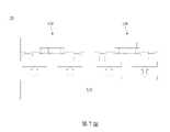
第6圖繪示本揭露一實施方式之顯示器60的上視示意圖。如第6圖所示,顯示器60包含驅動基板610以及如上所述之發光陣列結構10或30。發光陣列結構10或30設置於驅動基板610上。在多個實施例中,驅動基板610例如可為燈板、發光二極體陣列基板或電路板。當某一或某些發光畫素單元120產生瑕疵時,直接置換整個發光陣列結構10或30,可以達到簡易修復的效果。FIG. 6 shows a schematic top view of a
第7圖繪示本揭露又一實施方式之顯示器封裝70示意圖。如第7圖所示,可以將如第1圖所示的發光陣列結構10進行切割,以形成多個單一發光畫素單元120。再將這些單一發光畫素單元120各自依其特性進行分規(bining)後接合(bonding)於驅動基板610上。當某一發光畫素單元120產生瑕疵時,極易取下並直接置換整顆發光畫素單元120。這種方式不但具有易修復之優點,還可以減少失效分析以及修復工程的時間和材料成本。此外,先將單一發光畫素單元120進行分規後,再將相同規格之發光畫素單元120接合於同一驅動基板410上,可以解決視效不均的問題。相較於第7圖所示的顯示器封裝70,第6圖所示的顯示器60可以更進一步降低封裝體切割(dicing)、分規(bining)、打件(surface mount technology,SMT)及修復(repair)的成本。FIG. 7 shows a schematic diagram of a
第8圖繪示本揭露一實施方式之顯示器80的上視示意圖。如第8圖所示,顯示器80包含驅動基板610以及如前文之發光陣列結構40。多個發光陣列結構40設置於驅動基板610上。在多個實施例中,驅動基板610例如可為燈板、發光二極體陣列基板或電路板。當某一或某些發光畫素單元460產生瑕疵時,直接置換整個發光陣列結構40,可以達到簡易修復的效果。FIG. 8 shows a schematic top view of a
綜上所述,本揭露的發光陣列結構利用了多層平坦層減緩原本重佈線路層預計爬升的地段差,使得各層重佈線路層得以平舖在平坦層上,進而能夠維持較細較薄的高精度線路。而且,在製作重佈線路層的同時,可以一併製作顯示器的行列訊號線,以達到線路整合的優點。再者,重佈線路層的表面平整度遠優於基板的表面平整度,對於巨量轉移技術而言有較佳的轉移良率。本揭露的設計無需使用具有高精度線路的基板,且能夠輕易地微型化發光陣列結構。此外,本揭露的顯示器具有易修復之特性。To sum up, the light-emitting array structure disclosed in this disclosure uses multiple flat layers to slow down the expected climb of the original redistribution circuit layer, so that each layer of redistribution circuit layers can be tiled on the flat layer, thereby maintaining a thinner and thinner layer. High precision circuit. Moreover, while making the redistribution circuit layer, the row and column signal lines of the display can be produced at the same time, so as to achieve the advantage of circuit integration. Furthermore, the surface flatness of the redistribution wiring layer is much better than that of the substrate, which has a better transfer yield for the mass transfer technology. The design of the present disclosure does not need to use a substrate with high-precision circuits, and can easily miniaturize the light-emitting array structure. In addition, the display of the present disclosure is easy to repair.
雖然本揭露已以實施方式揭露如上,然其並非用以限定本揭露,任何熟習此技藝者,在不脫離本揭露之精神和範圍內,當可作各種之更動與潤飾,因此本揭露之保護範圍當視後附之申請專利範圍所界定者為準。Although this disclosure has been disclosed as above in the form of implementation, it is not intended to limit this disclosure. Anyone who is familiar with this technology can make various changes and modifications without departing from the spirit and scope of this disclosure. Therefore, the protection of this disclosure The scope shall be defined by the appended patent application scope.
10:發光陣列結構 110:基板 110a:上表面 110b:下表面 112:導電孔 114:第一導電墊 116:第二導電墊 120:發光畫素單元 121:驅動晶片 122:第一平坦層 123:第一重佈線路層 124:第二平坦層 125:第二重佈線路層 126:發光二極體 130:第一訊號線 140:第二訊號線 150:封裝層 30:發光陣列結構 310:反射層 40:發光陣列結構 410:驅動晶片 420:第一平坦層 430:第一重佈線路層 440:第二平坦層 450:第二重佈線路層 460:發光畫素單元 462:紅色發光二極體 464:綠色發光二極體 466:藍色發光二極體 470:第一訊號線 480:第二訊號線 60:顯示器 610:驅動基板 70:顯示器封裝 80:顯示器 D1:第一方向 D2:第二方向10:Light-emitting array structure 110:
為讓本揭露之上述和其他目的、特徵、優點與實施例能更明顯易懂,所附圖式之說明如下: 第1圖繪示本揭露一實施方式之發光陣列結構的上視示意圖。 第2圖繪示本揭露一實施方式之發光陣列結構的側視示意圖。 第3圖繪示本揭露另一實施方式之發光陣列結構的側視示意圖。 第4圖繪示本揭露一實施方式之發光陣列結構的上視示意圖。 第5圖繪示本揭露一實施方式之發光陣列結構的剖面示意圖。 第6圖繪示本揭露一實施方式之顯示器的上視示意圖。 第7圖繪示本揭露一實施方式之顯示器封裝示意圖。 第8圖繪示本揭露一實施方式之顯示器的上視示意圖。In order to make the above and other purposes, features, advantages and embodiments of the present disclosure more comprehensible, the accompanying drawings are described as follows: FIG. 1 shows a schematic top view of a light emitting array structure according to an embodiment of the present disclosure. FIG. 2 shows a schematic side view of a light emitting array structure according to an embodiment of the present disclosure. FIG. 3 shows a schematic side view of a light emitting array structure according to another embodiment of the present disclosure. FIG. 4 shows a schematic top view of a light emitting array structure according to an embodiment of the present disclosure. FIG. 5 shows a schematic cross-sectional view of a light emitting array structure according to an embodiment of the present disclosure. FIG. 6 is a schematic top view of a display according to an embodiment of the present disclosure. FIG. 7 shows a schematic diagram of a display package according to an embodiment of the present disclosure. FIG. 8 is a schematic top view of a display according to an embodiment of the present disclosure.
10:發光陣列結構10:Light-emitting array structure
110:基板110: Substrate
120:發光畫素單元120: Luminous pixel unit
121:驅動晶片121: Driver chip
124:第二平坦層124: second flat layer
126:發光二極體126: light emitting diode
130:第一訊號線130: The first signal line
140:第二訊號線140: Second signal line
D1:第一方向D1: the first direction
D2:第二方向D2: Second direction
Claims (19)
Translated fromChinesePriority Applications (1)
| Application Number | Priority Date | Filing Date | Title |
|---|---|---|---|
| US17/313,023US12094861B2 (en) | 2020-09-18 | 2021-05-06 | Light emitting array structure and display |
Applications Claiming Priority (2)
| Application Number | Priority Date | Filing Date | Title |
|---|---|---|---|
| TW109132460 | 2020-09-18 | ||
| TW109132460 | 2020-09-18 |
Publications (2)
| Publication Number | Publication Date |
|---|---|
| TW202213309A TW202213309A (en) | 2022-04-01 |
| TWI782401Btrue TWI782401B (en) | 2022-11-01 |
Family
ID=80740862
Family Applications (1)
| Application Number | Title | Priority Date | Filing Date |
|---|---|---|---|
| TW110102882ATWI782401B (en) | 2020-09-18 | 2021-01-26 | Light emitting array structure and display |
Country Status (2)
| Country | Link |
|---|---|
| US (1) | US11610875B2 (en) |
| TW (1) | TWI782401B (en) |
Families Citing this family (3)
| Publication number | Priority date | Publication date | Assignee | Title |
|---|---|---|---|---|
| US20230005985A1 (en)* | 2021-07-02 | 2023-01-05 | Samsung Electronics Co., Ltd. | Display layer having monolithic structure and display device including the display layer |
| TWI807909B (en)* | 2022-07-08 | 2023-07-01 | 宏齊科技股份有限公司 | Wafer-level full-color display device and manufacturing thereof |
| TWI824887B (en)* | 2022-12-16 | 2023-12-01 | 友達光電股份有限公司 | Display panel |
Citations (7)
| Publication number | Priority date | Publication date | Assignee | Title |
|---|---|---|---|---|
| TW200718347A (en)* | 2005-07-14 | 2007-05-01 | Mitsui Mining & Smelting Co | Blackening surface treated copper foil and electromagnetic wave shielding conductive mesh for front panel of plasma display using the blackening surface treated copper foil |
| TW200834876A (en)* | 2007-01-03 | 2008-08-16 | Advanced Chip Eng Tech Inc | Multi-chips package and method of forming the same |
| CN103594054A (en)* | 2012-08-17 | 2014-02-19 | 聚积科技股份有限公司 | Display structure and display |
| US20180261149A1 (en)* | 2015-08-06 | 2018-09-13 | Yi Lin | Led pixel,led component ,led panel and led display screen |
| TW201833890A (en)* | 2017-01-04 | 2018-09-16 | 南韓商三星顯示器有限公司 | Display device |
| US20190371229A1 (en)* | 2018-05-31 | 2019-12-05 | Invensas Corporation | Formation of a Light-Emitting Diode Display |
| TW202015261A (en)* | 2018-10-12 | 2020-04-16 | 欣興電子股份有限公司 | Light emitting device package structure and manufacturing method thereof |
Family Cites Families (9)
| Publication number | Priority date | Publication date | Assignee | Title |
|---|---|---|---|---|
| US10453398B2 (en) | 2013-06-20 | 2019-10-22 | Sharp Kabushiki Kaisha | Display apparatus and driving method thereof |
| US9368454B2 (en) | 2013-10-10 | 2016-06-14 | Taiwan Semiconductor Manufacturing Co., Ltd. | Semiconductor device with shielding layer in post-passivation interconnect structure |
| US10488961B2 (en) | 2015-07-17 | 2019-11-26 | Innolux Corporation | Gate driving circuit for driving a pixel array having a trigger circuit for receiving a touch sensing signal |
| JP7034423B2 (en) | 2016-04-28 | 2022-03-14 | オムニヴィジョン ティーディーディーアイ オンタリオ リミテッド パートナーシップ | Drive control devices and electronic devices |
| US10360846B2 (en) | 2016-05-10 | 2019-07-23 | X-Celeprint Limited | Distributed pulse-width modulation system with multi-bit digital storage and output device |
| KR102752222B1 (en) | 2016-11-11 | 2025-01-13 | 삼성디스플레이 주식회사 | Display apparatus and method of operating the same |
| CN108319385B (en) | 2016-12-23 | 2021-06-25 | 鸿富锦精密工业(深圳)有限公司 | Shift register and touch display device with shift register |
| CN106531051B (en) | 2017-01-03 | 2019-05-03 | 京东方科技集团股份有限公司 | Shift register unit and driving method thereof, gate driving circuit and display device |
| US10832609B2 (en) | 2017-01-10 | 2020-11-10 | X Display Company Technology Limited | Digital-drive pulse-width-modulated output system |
- 2020
- 2020-11-22USUS17/100,933patent/US11610875B2/enactiveActive
- 2021
- 2021-01-26TWTW110102882Apatent/TWI782401B/enactive
Patent Citations (7)
| Publication number | Priority date | Publication date | Assignee | Title |
|---|---|---|---|---|
| TW200718347A (en)* | 2005-07-14 | 2007-05-01 | Mitsui Mining & Smelting Co | Blackening surface treated copper foil and electromagnetic wave shielding conductive mesh for front panel of plasma display using the blackening surface treated copper foil |
| TW200834876A (en)* | 2007-01-03 | 2008-08-16 | Advanced Chip Eng Tech Inc | Multi-chips package and method of forming the same |
| CN103594054A (en)* | 2012-08-17 | 2014-02-19 | 聚积科技股份有限公司 | Display structure and display |
| US20180261149A1 (en)* | 2015-08-06 | 2018-09-13 | Yi Lin | Led pixel,led component ,led panel and led display screen |
| TW201833890A (en)* | 2017-01-04 | 2018-09-16 | 南韓商三星顯示器有限公司 | Display device |
| US20190371229A1 (en)* | 2018-05-31 | 2019-12-05 | Invensas Corporation | Formation of a Light-Emitting Diode Display |
| TW202015261A (en)* | 2018-10-12 | 2020-04-16 | 欣興電子股份有限公司 | Light emitting device package structure and manufacturing method thereof |
Also Published As
| Publication number | Publication date |
|---|---|
| TW202213309A (en) | 2022-04-01 |
| US20220093577A1 (en) | 2022-03-24 |
| US11610875B2 (en) | 2023-03-21 |
Similar Documents
| Publication | Publication Date | Title |
|---|---|---|
| TWI745206B (en) | Light emitting unit and display apparatus | |
| US10790267B2 (en) | Light emitting element for pixel and LED display module | |
| US12094861B2 (en) | Light emitting array structure and display | |
| US10782002B2 (en) | LED optical components | |
| TWI782401B (en) | Light emitting array structure and display | |
| US20180145236A1 (en) | Package structure for light emitting device | |
| US8283691B2 (en) | Light emitting device package and a lighting device | |
| CN210403726U (en) | Light Emitting Diode Package | |
| US11961951B2 (en) | Light emitting diode device | |
| US12020630B1 (en) | Stacked structure, display screen, and display apparatus | |
| CN109950380B (en) | Light Emitting Diode Package | |
| CN210403768U (en) | Light emitting diode packaging assembly | |
| JP7410752B2 (en) | Package structure and its electronics | |
| KR102585406B1 (en) | Light emitting device package | |
| TW201622100A (en) | Package structure for light emitting devices | |
| CN113224104A (en) | Micro light-emitting diode display device | |
| US10797210B2 (en) | Light emitting device having reduced thickness and increased light-reflectivity | |
| CN117637971A (en) | Display panels and display devices | |
| JP2023172904A (en) | pixel structure | |
| TWI805278B (en) | Light emitting module, display device, and manufacturing method of light emitting module | |
| US20240178197A1 (en) | Micro light-emitting diode display device and manufacturing method of the same | |
| CN111668361A (en) | Package structure and its manufacturing method and electronic device | |
| CN113903760A (en) | A stack structure, display screen and display device | |
| CN119208349A (en) | A display device |