TWI782400B - Semiconductor device and method of manufacturing the same - Google Patents
Semiconductor device and method of manufacturing the sameDownload PDFInfo
- Publication number
- TWI782400B TWI782400BTW110102842ATW110102842ATWI782400BTW I782400 BTWI782400 BTW I782400BTW 110102842 ATW110102842 ATW 110102842ATW 110102842 ATW110102842 ATW 110102842ATW I782400 BTWI782400 BTW I782400B
- Authority
- TW
- Taiwan
- Prior art keywords
- insulating film
- substrate
- semiconductor device
- opening
- plug
- Prior art date
Links
Images


Classifications
- H—ELECTRICITY
- H01—ELECTRIC ELEMENTS
- H01L—SEMICONDUCTOR DEVICES NOT COVERED BY CLASS H10
- H01L23/00—Details of semiconductor or other solid state devices
- H01L23/48—Arrangements for conducting electric current to or from the solid state body in operation, e.g. leads, terminal arrangements ; Selection of materials therefor
- H01L23/481—Internal lead connections, e.g. via connections, feedthrough structures
- H—ELECTRICITY
- H01—ELECTRIC ELEMENTS
- H01L—SEMICONDUCTOR DEVICES NOT COVERED BY CLASS H10
- H01L21/00—Processes or apparatus adapted for the manufacture or treatment of semiconductor or solid state devices or of parts thereof
- H01L21/70—Manufacture or treatment of devices consisting of a plurality of solid state components formed in or on a common substrate or of parts thereof; Manufacture of integrated circuit devices or of parts thereof
- H01L21/71—Manufacture of specific parts of devices defined in group H01L21/70
- H01L21/768—Applying interconnections to be used for carrying current between separate components within a device comprising conductors and dielectrics
- H01L21/76898—Applying interconnections to be used for carrying current between separate components within a device comprising conductors and dielectrics formed through a semiconductor substrate
- H—ELECTRICITY
- H01—ELECTRIC ELEMENTS
- H01L—SEMICONDUCTOR DEVICES NOT COVERED BY CLASS H10
- H01L21/00—Processes or apparatus adapted for the manufacture or treatment of semiconductor or solid state devices or of parts thereof
- H01L21/70—Manufacture or treatment of devices consisting of a plurality of solid state components formed in or on a common substrate or of parts thereof; Manufacture of integrated circuit devices or of parts thereof
- H01L21/71—Manufacture of specific parts of devices defined in group H01L21/70
- H01L21/768—Applying interconnections to be used for carrying current between separate components within a device comprising conductors and dielectrics
- H01L21/76801—Applying interconnections to be used for carrying current between separate components within a device comprising conductors and dielectrics characterised by the formation and the after-treatment of the dielectrics, e.g. smoothing
- H01L21/76802—Applying interconnections to be used for carrying current between separate components within a device comprising conductors and dielectrics characterised by the formation and the after-treatment of the dielectrics, e.g. smoothing by forming openings in dielectrics
- H01L21/76805—Applying interconnections to be used for carrying current between separate components within a device comprising conductors and dielectrics characterised by the formation and the after-treatment of the dielectrics, e.g. smoothing by forming openings in dielectrics the opening being a via or contact hole penetrating the underlying conductor
- H—ELECTRICITY
- H01—ELECTRIC ELEMENTS
- H01L—SEMICONDUCTOR DEVICES NOT COVERED BY CLASS H10
- H01L23/00—Details of semiconductor or other solid state devices
- H01L23/52—Arrangements for conducting electric current within the device in operation from one component to another, i.e. interconnections, e.g. wires, lead frames
- H01L23/535—Arrangements for conducting electric current within the device in operation from one component to another, i.e. interconnections, e.g. wires, lead frames including internal interconnections, e.g. cross-under constructions
- H—ELECTRICITY
- H01—ELECTRIC ELEMENTS
- H01L—SEMICONDUCTOR DEVICES NOT COVERED BY CLASS H10
- H01L24/00—Arrangements for connecting or disconnecting semiconductor or solid-state bodies; Methods or apparatus related thereto
- H01L24/01—Means for bonding being attached to, or being formed on, the surface to be connected, e.g. chip-to-package, die-attach, "first-level" interconnects; Manufacturing methods related thereto
- H01L24/02—Bonding areas ; Manufacturing methods related thereto
- H01L24/07—Structure, shape, material or disposition of the bonding areas after the connecting process
- H01L24/09—Structure, shape, material or disposition of the bonding areas after the connecting process of a plurality of bonding areas
- H—ELECTRICITY
- H01—ELECTRIC ELEMENTS
- H01L—SEMICONDUCTOR DEVICES NOT COVERED BY CLASS H10
- H01L24/00—Arrangements for connecting or disconnecting semiconductor or solid-state bodies; Methods or apparatus related thereto
- H01L24/80—Methods for connecting semiconductor or other solid state bodies using means for bonding being attached to, or being formed on, the surface to be connected
- H01L24/82—Methods for connecting semiconductor or other solid state bodies using means for bonding being attached to, or being formed on, the surface to be connected by forming build-up interconnects at chip-level, e.g. for high density interconnects [HDI]
- H—ELECTRICITY
- H01—ELECTRIC ELEMENTS
- H01L—SEMICONDUCTOR DEVICES NOT COVERED BY CLASS H10
- H01L25/00—Assemblies consisting of a plurality of semiconductor or other solid state devices
- H01L25/03—Assemblies consisting of a plurality of semiconductor or other solid state devices all the devices being of a type provided for in a single subclass of subclasses H10B, H10D, H10F, H10H, H10K or H10N, e.g. assemblies of rectifier diodes
- H01L25/04—Assemblies consisting of a plurality of semiconductor or other solid state devices all the devices being of a type provided for in a single subclass of subclasses H10B, H10D, H10F, H10H, H10K or H10N, e.g. assemblies of rectifier diodes the devices not having separate containers
- H01L25/065—Assemblies consisting of a plurality of semiconductor or other solid state devices all the devices being of a type provided for in a single subclass of subclasses H10B, H10D, H10F, H10H, H10K or H10N, e.g. assemblies of rectifier diodes the devices not having separate containers the devices being of a type provided for in group H10D89/00
- H01L25/0657—Stacked arrangements of devices
- H—ELECTRICITY
- H01—ELECTRIC ELEMENTS
- H01L—SEMICONDUCTOR DEVICES NOT COVERED BY CLASS H10
- H01L25/00—Assemblies consisting of a plurality of semiconductor or other solid state devices
- H01L25/18—Assemblies consisting of a plurality of semiconductor or other solid state devices the devices being of the types provided for in two or more different main groups of the same subclass of H10B, H10D, H10F, H10H, H10K or H10N
- H—ELECTRICITY
- H01—ELECTRIC ELEMENTS
- H01L—SEMICONDUCTOR DEVICES NOT COVERED BY CLASS H10
- H01L25/00—Assemblies consisting of a plurality of semiconductor or other solid state devices
- H01L25/50—Multistep manufacturing processes of assemblies consisting of devices, the devices being individual devices of subclass H10D or integrated devices of class H10
- H—ELECTRICITY
- H10—SEMICONDUCTOR DEVICES; ELECTRIC SOLID-STATE DEVICES NOT OTHERWISE PROVIDED FOR
- H10B—ELECTRONIC MEMORY DEVICES
- H10B43/00—EEPROM devices comprising charge-trapping gate insulators
- H10B43/20—EEPROM devices comprising charge-trapping gate insulators characterised by three-dimensional arrangements, e.g. with cells on different height levels
- H10B43/23—EEPROM devices comprising charge-trapping gate insulators characterised by three-dimensional arrangements, e.g. with cells on different height levels with source and drain on different levels, e.g. with sloping channels
- H10B43/27—EEPROM devices comprising charge-trapping gate insulators characterised by three-dimensional arrangements, e.g. with cells on different height levels with source and drain on different levels, e.g. with sloping channels the channels comprising vertical portions, e.g. U-shaped channels
- H—ELECTRICITY
- H10—SEMICONDUCTOR DEVICES; ELECTRIC SOLID-STATE DEVICES NOT OTHERWISE PROVIDED FOR
- H10B—ELECTRONIC MEMORY DEVICES
- H10B43/00—EEPROM devices comprising charge-trapping gate insulators
- H10B43/40—EEPROM devices comprising charge-trapping gate insulators characterised by the peripheral circuit region
- H—ELECTRICITY
- H01—ELECTRIC ELEMENTS
- H01L—SEMICONDUCTOR DEVICES NOT COVERED BY CLASS H10
- H01L2224/00—Indexing scheme for arrangements for connecting or disconnecting semiconductor or solid-state bodies and methods related thereto as covered by H01L24/00
- H01L2224/01—Means for bonding being attached to, or being formed on, the surface to be connected, e.g. chip-to-package, die-attach, "first-level" interconnects; Manufacturing methods related thereto
- H01L2224/02—Bonding areas; Manufacturing methods related thereto
- H01L2224/023—Redistribution layers [RDL] for bonding areas
- H01L2224/0237—Disposition of the redistribution layers
- H01L2224/02372—Disposition of the redistribution layers connecting to a via connection in the semiconductor or solid-state body
- H—ELECTRICITY
- H01—ELECTRIC ELEMENTS
- H01L—SEMICONDUCTOR DEVICES NOT COVERED BY CLASS H10
- H01L2224/00—Indexing scheme for arrangements for connecting or disconnecting semiconductor or solid-state bodies and methods related thereto as covered by H01L24/00
- H01L2224/01—Means for bonding being attached to, or being formed on, the surface to be connected, e.g. chip-to-package, die-attach, "first-level" interconnects; Manufacturing methods related thereto
- H01L2224/02—Bonding areas; Manufacturing methods related thereto
- H01L2224/03—Manufacturing methods
- H01L2224/034—Manufacturing methods by blanket deposition of the material of the bonding area
- H—ELECTRICITY
- H01—ELECTRIC ELEMENTS
- H01L—SEMICONDUCTOR DEVICES NOT COVERED BY CLASS H10
- H01L2224/00—Indexing scheme for arrangements for connecting or disconnecting semiconductor or solid-state bodies and methods related thereto as covered by H01L24/00
- H01L2224/01—Means for bonding being attached to, or being formed on, the surface to be connected, e.g. chip-to-package, die-attach, "first-level" interconnects; Manufacturing methods related thereto
- H01L2224/02—Bonding areas; Manufacturing methods related thereto
- H01L2224/03—Manufacturing methods
- H01L2224/036—Manufacturing methods by patterning a pre-deposited material
- H01L2224/0361—Physical or chemical etching
- H—ELECTRICITY
- H01—ELECTRIC ELEMENTS
- H01L—SEMICONDUCTOR DEVICES NOT COVERED BY CLASS H10
- H01L2224/00—Indexing scheme for arrangements for connecting or disconnecting semiconductor or solid-state bodies and methods related thereto as covered by H01L24/00
- H01L2224/01—Means for bonding being attached to, or being formed on, the surface to be connected, e.g. chip-to-package, die-attach, "first-level" interconnects; Manufacturing methods related thereto
- H01L2224/02—Bonding areas; Manufacturing methods related thereto
- H01L2224/03—Manufacturing methods
- H01L2224/036—Manufacturing methods by patterning a pre-deposited material
- H01L2224/03622—Manufacturing methods by patterning a pre-deposited material using masks
- H—ELECTRICITY
- H01—ELECTRIC ELEMENTS
- H01L—SEMICONDUCTOR DEVICES NOT COVERED BY CLASS H10
- H01L2224/00—Indexing scheme for arrangements for connecting or disconnecting semiconductor or solid-state bodies and methods related thereto as covered by H01L24/00
- H01L2224/01—Means for bonding being attached to, or being formed on, the surface to be connected, e.g. chip-to-package, die-attach, "first-level" interconnects; Manufacturing methods related thereto
- H01L2224/02—Bonding areas; Manufacturing methods related thereto
- H01L2224/04—Structure, shape, material or disposition of the bonding areas prior to the connecting process
- H01L2224/0401—Bonding areas specifically adapted for bump connectors, e.g. under bump metallisation [UBM]
- H—ELECTRICITY
- H01—ELECTRIC ELEMENTS
- H01L—SEMICONDUCTOR DEVICES NOT COVERED BY CLASS H10
- H01L2224/00—Indexing scheme for arrangements for connecting or disconnecting semiconductor or solid-state bodies and methods related thereto as covered by H01L24/00
- H01L2224/01—Means for bonding being attached to, or being formed on, the surface to be connected, e.g. chip-to-package, die-attach, "first-level" interconnects; Manufacturing methods related thereto
- H01L2224/02—Bonding areas; Manufacturing methods related thereto
- H01L2224/04—Structure, shape, material or disposition of the bonding areas prior to the connecting process
- H01L2224/04042—Bonding areas specifically adapted for wire connectors, e.g. wirebond pads
- H—ELECTRICITY
- H01—ELECTRIC ELEMENTS
- H01L—SEMICONDUCTOR DEVICES NOT COVERED BY CLASS H10
- H01L2224/00—Indexing scheme for arrangements for connecting or disconnecting semiconductor or solid-state bodies and methods related thereto as covered by H01L24/00
- H01L2224/01—Means for bonding being attached to, or being formed on, the surface to be connected, e.g. chip-to-package, die-attach, "first-level" interconnects; Manufacturing methods related thereto
- H01L2224/02—Bonding areas; Manufacturing methods related thereto
- H01L2224/04—Structure, shape, material or disposition of the bonding areas prior to the connecting process
- H01L2224/05—Structure, shape, material or disposition of the bonding areas prior to the connecting process of an individual bonding area
- H01L2224/0554—External layer
- H01L2224/05541—Structure
- H01L2224/05548—Bonding area integrally formed with a redistribution layer on the semiconductor or solid-state body
- H—ELECTRICITY
- H01—ELECTRIC ELEMENTS
- H01L—SEMICONDUCTOR DEVICES NOT COVERED BY CLASS H10
- H01L2224/00—Indexing scheme for arrangements for connecting or disconnecting semiconductor or solid-state bodies and methods related thereto as covered by H01L24/00
- H01L2224/01—Means for bonding being attached to, or being formed on, the surface to be connected, e.g. chip-to-package, die-attach, "first-level" interconnects; Manufacturing methods related thereto
- H01L2224/02—Bonding areas; Manufacturing methods related thereto
- H01L2224/04—Structure, shape, material or disposition of the bonding areas prior to the connecting process
- H01L2224/05—Structure, shape, material or disposition of the bonding areas prior to the connecting process of an individual bonding area
- H01L2224/0554—External layer
- H01L2224/0556—Disposition
- H01L2224/05567—Disposition the external layer being at least partially embedded in the surface
- H—ELECTRICITY
- H01—ELECTRIC ELEMENTS
- H01L—SEMICONDUCTOR DEVICES NOT COVERED BY CLASS H10
- H01L2224/00—Indexing scheme for arrangements for connecting or disconnecting semiconductor or solid-state bodies and methods related thereto as covered by H01L24/00
- H01L2224/01—Means for bonding being attached to, or being formed on, the surface to be connected, e.g. chip-to-package, die-attach, "first-level" interconnects; Manufacturing methods related thereto
- H01L2224/02—Bonding areas; Manufacturing methods related thereto
- H01L2224/07—Structure, shape, material or disposition of the bonding areas after the connecting process
- H01L2224/08—Structure, shape, material or disposition of the bonding areas after the connecting process of an individual bonding area
- H01L2224/081—Disposition
- H01L2224/0812—Disposition the bonding area connecting directly to another bonding area, i.e. connectorless bonding, e.g. bumpless bonding
- H01L2224/08135—Disposition the bonding area connecting directly to another bonding area, i.e. connectorless bonding, e.g. bumpless bonding the bonding area connecting between different semiconductor or solid-state bodies, i.e. chip-to-chip
- H01L2224/08145—Disposition the bonding area connecting directly to another bonding area, i.e. connectorless bonding, e.g. bumpless bonding the bonding area connecting between different semiconductor or solid-state bodies, i.e. chip-to-chip the bodies being stacked
- H—ELECTRICITY
- H01—ELECTRIC ELEMENTS
- H01L—SEMICONDUCTOR DEVICES NOT COVERED BY CLASS H10
- H01L2224/00—Indexing scheme for arrangements for connecting or disconnecting semiconductor or solid-state bodies and methods related thereto as covered by H01L24/00
- H01L2224/01—Means for bonding being attached to, or being formed on, the surface to be connected, e.g. chip-to-package, die-attach, "first-level" interconnects; Manufacturing methods related thereto
- H01L2224/02—Bonding areas; Manufacturing methods related thereto
- H01L2224/07—Structure, shape, material or disposition of the bonding areas after the connecting process
- H01L2224/09—Structure, shape, material or disposition of the bonding areas after the connecting process of a plurality of bonding areas
- H01L2224/091—Disposition
- H01L2224/0918—Disposition being disposed on at least two different sides of the body, e.g. dual array
- H01L2224/09181—On opposite sides of the body
- H—ELECTRICITY
- H01—ELECTRIC ELEMENTS
- H01L—SEMICONDUCTOR DEVICES NOT COVERED BY CLASS H10
- H01L2224/00—Indexing scheme for arrangements for connecting or disconnecting semiconductor or solid-state bodies and methods related thereto as covered by H01L24/00
- H01L2224/80—Methods for connecting semiconductor or other solid state bodies using means for bonding being attached to, or being formed on, the surface to be connected
- H01L2224/80001—Methods for connecting semiconductor or other solid state bodies using means for bonding being attached to, or being formed on, the surface to be connected by connecting a bonding area directly to another bonding area, i.e. connectorless bonding, e.g. bumpless bonding
- H01L2224/80053—Bonding environment
- H01L2224/80095—Temperature settings
- H01L2224/80096—Transient conditions
- H01L2224/80097—Heating
- H—ELECTRICITY
- H01—ELECTRIC ELEMENTS
- H01L—SEMICONDUCTOR DEVICES NOT COVERED BY CLASS H10
- H01L2224/00—Indexing scheme for arrangements for connecting or disconnecting semiconductor or solid-state bodies and methods related thereto as covered by H01L24/00
- H01L2224/80—Methods for connecting semiconductor or other solid state bodies using means for bonding being attached to, or being formed on, the surface to be connected
- H01L2224/80001—Methods for connecting semiconductor or other solid state bodies using means for bonding being attached to, or being formed on, the surface to be connected by connecting a bonding area directly to another bonding area, i.e. connectorless bonding, e.g. bumpless bonding
- H01L2224/802—Applying energy for connecting
- H01L2224/80201—Compression bonding
- H—ELECTRICITY
- H01—ELECTRIC ELEMENTS
- H01L—SEMICONDUCTOR DEVICES NOT COVERED BY CLASS H10
- H01L2224/00—Indexing scheme for arrangements for connecting or disconnecting semiconductor or solid-state bodies and methods related thereto as covered by H01L24/00
- H01L2224/80—Methods for connecting semiconductor or other solid state bodies using means for bonding being attached to, or being formed on, the surface to be connected
- H01L2224/80001—Methods for connecting semiconductor or other solid state bodies using means for bonding being attached to, or being formed on, the surface to be connected by connecting a bonding area directly to another bonding area, i.e. connectorless bonding, e.g. bumpless bonding
- H01L2224/8034—Bonding interfaces of the bonding area
- H01L2224/80357—Bonding interfaces of the bonding area being flush with the surface
- H—ELECTRICITY
- H01—ELECTRIC ELEMENTS
- H01L—SEMICONDUCTOR DEVICES NOT COVERED BY CLASS H10
- H01L2224/00—Indexing scheme for arrangements for connecting or disconnecting semiconductor or solid-state bodies and methods related thereto as covered by H01L24/00
- H01L2224/80—Methods for connecting semiconductor or other solid state bodies using means for bonding being attached to, or being formed on, the surface to be connected
- H01L2224/80001—Methods for connecting semiconductor or other solid state bodies using means for bonding being attached to, or being formed on, the surface to be connected by connecting a bonding area directly to another bonding area, i.e. connectorless bonding, e.g. bumpless bonding
- H01L2224/808—Bonding techniques
- H01L2224/80894—Direct bonding, i.e. joining surfaces by means of intermolecular attracting interactions at their interfaces, e.g. covalent bonds, van der Waals forces
- H01L2224/80895—Direct bonding, i.e. joining surfaces by means of intermolecular attracting interactions at their interfaces, e.g. covalent bonds, van der Waals forces between electrically conductive surfaces, e.g. copper-copper direct bonding, surface activated bonding
- H—ELECTRICITY
- H01—ELECTRIC ELEMENTS
- H01L—SEMICONDUCTOR DEVICES NOT COVERED BY CLASS H10
- H01L2224/00—Indexing scheme for arrangements for connecting or disconnecting semiconductor or solid-state bodies and methods related thereto as covered by H01L24/00
- H01L2224/80—Methods for connecting semiconductor or other solid state bodies using means for bonding being attached to, or being formed on, the surface to be connected
- H01L2224/80001—Methods for connecting semiconductor or other solid state bodies using means for bonding being attached to, or being formed on, the surface to be connected by connecting a bonding area directly to another bonding area, i.e. connectorless bonding, e.g. bumpless bonding
- H01L2224/808—Bonding techniques
- H01L2224/80894—Direct bonding, i.e. joining surfaces by means of intermolecular attracting interactions at their interfaces, e.g. covalent bonds, van der Waals forces
- H01L2224/80896—Direct bonding, i.e. joining surfaces by means of intermolecular attracting interactions at their interfaces, e.g. covalent bonds, van der Waals forces between electrically insulating surfaces, e.g. oxide or nitride layers
- H—ELECTRICITY
- H01—ELECTRIC ELEMENTS
- H01L—SEMICONDUCTOR DEVICES NOT COVERED BY CLASS H10
- H01L2224/00—Indexing scheme for arrangements for connecting or disconnecting semiconductor or solid-state bodies and methods related thereto as covered by H01L24/00
- H01L2224/80—Methods for connecting semiconductor or other solid state bodies using means for bonding being attached to, or being formed on, the surface to be connected
- H01L2224/80001—Methods for connecting semiconductor or other solid state bodies using means for bonding being attached to, or being formed on, the surface to be connected by connecting a bonding area directly to another bonding area, i.e. connectorless bonding, e.g. bumpless bonding
- H01L2224/80905—Combinations of bonding methods provided for in at least two different groups from H01L2224/808 - H01L2224/80904
- H01L2224/80906—Specific sequence of method steps
- H—ELECTRICITY
- H01—ELECTRIC ELEMENTS
- H01L—SEMICONDUCTOR DEVICES NOT COVERED BY CLASS H10
- H01L2224/00—Indexing scheme for arrangements for connecting or disconnecting semiconductor or solid-state bodies and methods related thereto as covered by H01L24/00
- H01L2224/80—Methods for connecting semiconductor or other solid state bodies using means for bonding being attached to, or being formed on, the surface to be connected
- H01L2224/80001—Methods for connecting semiconductor or other solid state bodies using means for bonding being attached to, or being formed on, the surface to be connected by connecting a bonding area directly to another bonding area, i.e. connectorless bonding, e.g. bumpless bonding
- H01L2224/80909—Post-treatment of the bonding area
- H01L2224/80948—Thermal treatments, e.g. annealing, controlled cooling
- H—ELECTRICITY
- H01—ELECTRIC ELEMENTS
- H01L—SEMICONDUCTOR DEVICES NOT COVERED BY CLASS H10
- H01L2224/00—Indexing scheme for arrangements for connecting or disconnecting semiconductor or solid-state bodies and methods related thereto as covered by H01L24/00
- H01L2224/91—Methods for connecting semiconductor or solid state bodies including different methods provided for in two or more of groups H01L2224/80 - H01L2224/90
- H01L2224/92—Specific sequence of method steps
- H01L2224/9202—Forming additional connectors after the connecting process
- H—ELECTRICITY
- H01—ELECTRIC ELEMENTS
- H01L—SEMICONDUCTOR DEVICES NOT COVERED BY CLASS H10
- H01L2224/00—Indexing scheme for arrangements for connecting or disconnecting semiconductor or solid-state bodies and methods related thereto as covered by H01L24/00
- H01L2224/93—Batch processes
- H01L2224/94—Batch processes at wafer-level, i.e. with connecting carried out on a wafer comprising a plurality of undiced individual devices
- H—ELECTRICITY
- H01—ELECTRIC ELEMENTS
- H01L—SEMICONDUCTOR DEVICES NOT COVERED BY CLASS H10
- H01L2225/00—Details relating to assemblies covered by the group H01L25/00 but not provided for in its subgroups
- H01L2225/03—All the devices being of a type provided for in the same main group of the same subclass of class H10, e.g. assemblies of rectifier diodes
- H01L2225/04—All the devices being of a type provided for in the same main group of the same subclass of class H10, e.g. assemblies of rectifier diodes the devices not having separate containers
- H01L2225/065—All the devices being of a type provided for in the same main group of the same subclass of class H10
- H01L2225/06503—Stacked arrangements of devices
- H01L2225/0651—Wire or wire-like electrical connections from device to substrate
- H—ELECTRICITY
- H01—ELECTRIC ELEMENTS
- H01L—SEMICONDUCTOR DEVICES NOT COVERED BY CLASS H10
- H01L2225/00—Details relating to assemblies covered by the group H01L25/00 but not provided for in its subgroups
- H01L2225/03—All the devices being of a type provided for in the same main group of the same subclass of class H10, e.g. assemblies of rectifier diodes
- H01L2225/04—All the devices being of a type provided for in the same main group of the same subclass of class H10, e.g. assemblies of rectifier diodes the devices not having separate containers
- H01L2225/065—All the devices being of a type provided for in the same main group of the same subclass of class H10
- H01L2225/06503—Stacked arrangements of devices
- H01L2225/06517—Bump or bump-like direct electrical connections from device to substrate
- H—ELECTRICITY
- H01—ELECTRIC ELEMENTS
- H01L—SEMICONDUCTOR DEVICES NOT COVERED BY CLASS H10
- H01L2225/00—Details relating to assemblies covered by the group H01L25/00 but not provided for in its subgroups
- H01L2225/03—All the devices being of a type provided for in the same main group of the same subclass of class H10, e.g. assemblies of rectifier diodes
- H01L2225/04—All the devices being of a type provided for in the same main group of the same subclass of class H10, e.g. assemblies of rectifier diodes the devices not having separate containers
- H01L2225/065—All the devices being of a type provided for in the same main group of the same subclass of class H10
- H01L2225/06503—Stacked arrangements of devices
- H01L2225/06524—Electrical connections formed on device or on substrate, e.g. a deposited or grown layer
- H—ELECTRICITY
- H01—ELECTRIC ELEMENTS
- H01L—SEMICONDUCTOR DEVICES NOT COVERED BY CLASS H10
- H01L2225/00—Details relating to assemblies covered by the group H01L25/00 but not provided for in its subgroups
- H01L2225/03—All the devices being of a type provided for in the same main group of the same subclass of class H10, e.g. assemblies of rectifier diodes
- H01L2225/04—All the devices being of a type provided for in the same main group of the same subclass of class H10, e.g. assemblies of rectifier diodes the devices not having separate containers
- H01L2225/065—All the devices being of a type provided for in the same main group of the same subclass of class H10
- H01L2225/06503—Stacked arrangements of devices
- H01L2225/06541—Conductive via connections through the device, e.g. vertical interconnects, through silicon via [TSV]
- H01L2225/06544—Design considerations for via connections, e.g. geometry or layout
- H—ELECTRICITY
- H01—ELECTRIC ELEMENTS
- H01L—SEMICONDUCTOR DEVICES NOT COVERED BY CLASS H10
- H01L24/00—Arrangements for connecting or disconnecting semiconductor or solid-state bodies; Methods or apparatus related thereto
- H01L24/01—Means for bonding being attached to, or being formed on, the surface to be connected, e.g. chip-to-package, die-attach, "first-level" interconnects; Manufacturing methods related thereto
- H01L24/02—Bonding areas ; Manufacturing methods related thereto
- H01L24/03—Manufacturing methods
- H—ELECTRICITY
- H01—ELECTRIC ELEMENTS
- H01L—SEMICONDUCTOR DEVICES NOT COVERED BY CLASS H10
- H01L24/00—Arrangements for connecting or disconnecting semiconductor or solid-state bodies; Methods or apparatus related thereto
- H01L24/01—Means for bonding being attached to, or being formed on, the surface to be connected, e.g. chip-to-package, die-attach, "first-level" interconnects; Manufacturing methods related thereto
- H01L24/02—Bonding areas ; Manufacturing methods related thereto
- H01L24/04—Structure, shape, material or disposition of the bonding areas prior to the connecting process
- H01L24/05—Structure, shape, material or disposition of the bonding areas prior to the connecting process of an individual bonding area
- H—ELECTRICITY
- H01—ELECTRIC ELEMENTS
- H01L—SEMICONDUCTOR DEVICES NOT COVERED BY CLASS H10
- H01L24/00—Arrangements for connecting or disconnecting semiconductor or solid-state bodies; Methods or apparatus related thereto
- H01L24/01—Means for bonding being attached to, or being formed on, the surface to be connected, e.g. chip-to-package, die-attach, "first-level" interconnects; Manufacturing methods related thereto
- H01L24/02—Bonding areas ; Manufacturing methods related thereto
- H01L24/07—Structure, shape, material or disposition of the bonding areas after the connecting process
- H01L24/08—Structure, shape, material or disposition of the bonding areas after the connecting process of an individual bonding area
- H—ELECTRICITY
- H01—ELECTRIC ELEMENTS
- H01L—SEMICONDUCTOR DEVICES NOT COVERED BY CLASS H10
- H01L2924/00—Indexing scheme for arrangements or methods for connecting or disconnecting semiconductor or solid-state bodies as covered by H01L24/00
- H01L2924/10—Details of semiconductor or other solid state devices to be connected
- H01L2924/11—Device type
- H01L2924/14—Integrated circuits
- H01L2924/143—Digital devices
- H01L2924/1431—Logic devices
- H—ELECTRICITY
- H01—ELECTRIC ELEMENTS
- H01L—SEMICONDUCTOR DEVICES NOT COVERED BY CLASS H10
- H01L2924/00—Indexing scheme for arrangements or methods for connecting or disconnecting semiconductor or solid-state bodies as covered by H01L24/00
- H01L2924/10—Details of semiconductor or other solid state devices to be connected
- H01L2924/11—Device type
- H01L2924/14—Integrated circuits
- H01L2924/143—Digital devices
- H01L2924/1434—Memory
- H01L2924/145—Read-only memory [ROM]
- H01L2924/1451—EPROM
- H01L2924/14511—EEPROM
- H—ELECTRICITY
- H10—SEMICONDUCTOR DEVICES; ELECTRIC SOLID-STATE DEVICES NOT OTHERWISE PROVIDED FOR
- H10B—ELECTRONIC MEMORY DEVICES
- H10B43/00—EEPROM devices comprising charge-trapping gate insulators
- H10B43/50—EEPROM devices comprising charge-trapping gate insulators characterised by the boundary region between the core and peripheral circuit regions
Landscapes
- Engineering & Computer Science (AREA)
- Microelectronics & Electronic Packaging (AREA)
- Power Engineering (AREA)
- Computer Hardware Design (AREA)
- Physics & Mathematics (AREA)
- Condensed Matter Physics & Semiconductors (AREA)
- General Physics & Mathematics (AREA)
- Manufacturing & Machinery (AREA)
- Internal Circuitry In Semiconductor Integrated Circuit Devices (AREA)
- Semiconductor Memories (AREA)
- Non-Volatile Memory (AREA)
- Design And Manufacture Of Integrated Circuits (AREA)
Abstract
Translated fromChineseDescription
Translated fromChinese本發明之實施形態係關於一種半導體裝置及其製造方法。Embodiments of the present invention relate to a semiconductor device and a manufacturing method thereof.
於基板上形成通孔插塞與接合墊之情形時,期望以較適宜之態樣將接合墊電性連接於通孔插塞。When forming via plugs and bonding pads on a substrate, it is desirable to electrically connect the bonding pads to the via plugs in a more suitable manner.
實施形態提供一種可以適宜之態樣將接合墊電性連接於通孔插塞之半導體裝置及其製造方法。The embodiment provides a semiconductor device and a manufacturing method thereof in which a bonding pad can be electrically connected to a via plug in an appropriate manner.
根據一實施形態,半導體裝置具備第1基板、及設置於上述第1基板上之第1絕緣膜。上述裝置進而具備:第1插塞,其設置於上述第1絕緣膜內;及第2基板,其設置於上述第1絕緣膜上。上述裝置進而具備第1配線,其包含:第1部分,其設置於上述第2基板內,且設置於上述第1插塞上;及第2部分,其設置於上述第2基板上,包含接合墊,且以與上述第1部分之材料相同之材料形成。According to one embodiment, a semiconductor device includes a first substrate and a first insulating film provided on the first substrate. The above device further includes: a first plug provided in the first insulating film; and a second substrate provided on the first insulating film. The above device further includes a first wiring including: a first part provided in the second substrate and provided on the first plug; and a second part provided on the second substrate and including a bonding Pads, and formed of the same material as in
以下,參照圖式說明本發明之實施形態。圖1至圖9中,對相同構成附注相同符號,省略重複之說明。Hereinafter, embodiments of the present invention will be described with reference to the drawings. In FIGS. 1 to 9 , the same symbols are assigned to the same configurations, and overlapping descriptions are omitted.
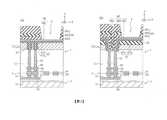
(第1實施形態) 圖1係顯示第1實施形態之半導體裝置之構造之剖視圖。圖1之半導體裝置係將陣列晶片1與電路晶片2加以貼合之3維記憶體。(first embodiment) FIG. 1 is a cross-sectional view showing the structure of a semiconductor device according to a first embodiment. The semiconductor device shown in FIG. 1 is a three-dimensional memory in which an
圖1表示互相垂直之X方向、Y方向及Z方向。本說明書中,將+Z方向作為上方向處理,將-Z方向作為下方向處理。-Z方向可與重力方向一致,亦可不與重力方向一致。FIG. 1 shows X direction, Y direction and Z direction which are perpendicular to each other. In this specification, the +Z direction is treated as an upward direction, and the -Z direction is treated as a downward direction. - The Z direction may or may not coincide with the direction of gravity.
陣列晶片1具備包含複數個記憶胞之記憶胞陣列11、記憶胞陣列11上之基板12、及記憶胞陣列11下之層間絕緣膜13。基板12例如為矽基板等半導體基板。圖1顯示形成於基板12內之井(well)區域12a。層間絕緣膜13例如為氧化矽膜、或包含氧化矽膜與其他絕緣膜之積層膜。基板12為第2基板之例。層間絕緣膜13為第1絕緣膜之例。The
電路晶片2設置於陣列晶片1下。圖1顯示陣列晶片1與電路晶片2之貼合面S。電路晶片2具備層間絕緣膜14、與層間絕緣膜14下之基板15。層間絕緣膜14例如為氧化矽膜、或包含氧化矽膜與其他絕緣膜之積層膜。基板15例如為矽基板等半導體基板。層間絕緣膜14與層間絕緣膜13皆為第1絕緣膜之例。基板15為第1基板之例。The
陣列晶片1具備複數條字元線WL作為記憶胞陣列11內之電極層。圖1顯示記憶胞陣列11內之階差構造部21。各字元線WL經由接觸插塞22及通孔插塞23與字元配線層WI電性連接。圖1中進而顯示貫通上述複數條字元線WL之複數個柱狀部CL中之一個。各柱狀部CL經由通孔插塞24與位元線BL電性連接。The
電路晶片2具備複數個電晶體31。圖1顯示該等電晶體31中之1個。各電晶體31具備介隔閘極絕緣膜設置於基板15上之閘極電極32、及設置於基板15內之未圖示之源極擴散層及汲極擴散層。又,電路晶片2具備:複數個接觸插塞33,其等設置於該等電晶體31之閘極電極32、源極擴散層或汲極擴散層上;配線層34,其設置於該等接觸插塞33上,包含複數條配線;及複數個通孔插塞35,其設置於配線層34上。The
電路晶片2進而具備:配線層36,其設置於該等通孔插塞35上,包含複數條配線;複數個通孔插塞37,其等設置於配線層36上;及複數個金屬焊墊38,其等設置於該等通孔插塞37上。金屬焊墊38例如為包含Cu層或Al層之金屬層(Cu表示銅,Al表示鋁)。電路晶片2作為控制陣列晶片1之動作之控制電路(邏輯電路)發揮功能。該控制電路由電晶體31等構成,電性連接於金屬焊墊38。The
陣列晶片1具備:複數個金屬焊墊41,其等設置於金屬焊墊38上;及複數個通孔插塞42,其等設置於金屬焊墊41上。又,陣列晶片1具備:配線層43,其設置於該等通孔插塞42上,包含複數條配線;及複數個通孔插塞44,其等設置於配線層43上。金屬焊墊41例如為包含Cu層或Al層之金屬層。上述位元線BL或字元配線層WI包含於配線層43。又,上述控制電路經由金屬焊墊41、38等電性連接於記憶胞陣列11,且經由金屬焊墊41、38等控制記憶胞陣列11之動作。The
陣列晶片1進而具備設置於上述複數個通孔插塞44上之複數個通孔插塞45。圖1顯示該等通孔插塞45中之2個。通孔插塞45設置於層間絕緣膜13內,設置於記憶胞陣列11之側方。通孔插塞45例如為包含W層之金屬層(W表示鎢)。通孔插塞45為第1插塞之例。The
陣列晶片1進而具備依序形成於基板12上之絕緣膜46、絕緣膜47及金屬配線48。絕緣膜46例如為氧化矽膜。絕緣膜47例如為氧化矽膜。金屬配線48例如為包含Al層之金屬層。絕緣膜46為第2絕緣膜或第1膜之例。絕緣膜47為第2絕緣膜或第2膜之例。金屬配線48為第1配線之例。The
絕緣膜47包含:側方部47a,其形成於基板12及絕緣膜46之側面;上方部47b,其形成於絕緣膜46之上表面;及埋入部47c,其埋入於基板12及絕緣膜46內。側方部47a及埋入部47c形成於基板12及絕緣膜46之內部,上方部47b形成於基板12及絕緣膜46之外部。本實施形態中,側方部47a作為基板12及絕緣膜46之側面之側壁絕緣膜發揮功能,埋入膜47c作為基板12及絕緣膜46內之元件分離絕緣膜發揮功能。本實施形態之埋入部47c包含將埋入部47埋入於基板12及絕緣膜46內時形成之氣隙AG。側方部47a為第3部分之例。埋入部47c為與第3部分不同之第4部分之例。The
金屬配線48包含:上方部48a,其形成於層間絕緣膜13及上述複數個通孔插塞45之上表面;側方部48b,其形成於絕緣膜47之側面;及上方部48c,其形成於絕緣膜47之上表面。金屬配線48電性連接於上述複數個通孔插塞45。上方部48a及側方部48b形成於基板12、絕緣膜46及絕緣膜47之內部,上方部48c形成於基板12、絕緣膜46及絕緣膜47之外部。因本實施形態之上方部48a、側方部48b及上方部48c由相同之配線層同時形成,故以相同之材料(例如鋁)形成。本實施形態之上方部48a、側方部48b及上方部48c形成連續之1條配線。上方部48a及側方部48b為第1部分之例。上方部48c為第2部分之例。The
陣列晶片1進而具備形成於絕緣膜47及金屬配線48上之鈍化膜49。鈍化膜49為第3絕緣膜之例。The
鈍化膜49包含依序形成於絕緣膜47及金屬配線48上之絕緣膜49a、絕緣膜49b、及絕緣膜49c。絕緣膜49a例如為氧化矽膜。絕緣膜49b例如為氮化矽膜。絕緣膜49c例如為聚醯亞胺膜。本實施形態之鈍化膜49如圖1所示包含介隔絕緣膜47(側方部47a)與金屬配線48(側方部48a)形成於基板12及絕緣膜46內之部分。The
鈍化膜49例如具有使金屬層48之上方部48c之上表面露出之開口部P。於開口部P內露出之上方部48c作為圖1之半導體裝置之外部連接墊(接合墊)發揮功能。上方部48c可經由開口部P利用接合線、焊料球、金屬凸塊等連接於安裝基板或其他裝置。The
本實施形態之金屬配線48包含:上方部48a,其設置於上述複數個通孔插塞45上;及上方部48c,其包含接合墊;且作為電性連接該等通孔插塞45與接合墊之連接配線發揮功能。與該1條金屬配線48電性連接之通孔插塞45之個數可為任意個,例如為100~10000個。The
陣列晶片1內之記憶胞陣列11包含與上述複數條字元線WL交替積層之複數個絕緣層51。絕緣層51例如為氧化矽膜。The
陣列晶片1內之各柱狀部CL包含記憶體絕緣膜52、通道半導體層53、芯絕緣膜54、半導體層55及半導體層56。記憶體絕緣膜52、通道半導體層53、及芯絕緣膜54依序形成於字元線WL及絕緣層51內。半導體層55形成於通道半導體層53上,電性連接通道半導體層53與基板12。半導體層56於芯絕緣膜54下形成於通道半導體層53之側面,且電性連接通道半導體層53與通孔插塞24。Each columnar portion CL in the
圖2係顯示第1實施形態之各柱狀部CL之構造之剖視圖。圖2相當於圖1之剖視圖之放大圖。Fig. 2 is a cross-sectional view showing the structure of each columnar portion CL in the first embodiment. FIG. 2 corresponds to an enlarged view of the cross-sectional view of FIG. 1 .
如圖2所示,記憶體絕緣膜52包含依序形成於字元線WL及絕緣層51內之阻擋絕緣膜52a、電荷蓄積層52b、及穿隧絕緣膜52c。阻擋絕緣膜52a、穿隧絕緣膜52c、及芯絕緣膜54例如為氧化矽膜或金屬絕緣膜。電荷蓄積層52b例如為氮化矽膜。電荷蓄積層52b亦可為多晶矽層等半導體層。通道半導體層53、半導體層55(圖1)及半導體層56(圖1)例如為多晶矽層或單晶矽層。As shown in FIG. 2 , the
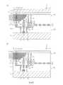
圖3係用於比較第1實施形態之半導體裝置及其比較例之半導體裝置之剖視圖。3 is a cross-sectional view for comparing the semiconductor device of the first embodiment and the semiconductor device of the comparative example.
圖3(a)顯示比較例之半導體裝置之構造。比較例之半導體裝置具有與本實施形態之半導體裝置大致相同之構造。但,比較例中,於上述複數個通孔插塞45上形成有複數個通孔插塞61,於該等通孔插塞61上形成有金屬配線48之上方部48c。比較例之金屬配線48不具備上方部48a或側方部48b。FIG. 3( a ) shows the structure of a semiconductor device of a comparative example. The semiconductor device of the comparative example has substantially the same structure as the semiconductor device of the present embodiment. However, in the comparative example, a plurality of via
圖3(a)所示之通孔插塞61與金屬配線48例如以如下方式形成。首先,於基板12內形成複數個通孔,於該等通孔內,使複數個通孔插塞45露出。接著,於該等通孔內介隔絕緣膜47形成通孔插塞61,於通孔插塞45上配置通孔插塞61。接著,於通孔插塞61上形成金屬配線48。The via
另一方面,圖3(b)顯示第1實施形態之半導體裝置之構造。圖3(b)所示之金屬配線48例如以如下方式形成。首先,於基板12內形成1個開口部,於該開口部內,使複數個通孔插塞45露出。接著,遍及該開口部之內部與外部形成金屬配線48,於通孔插塞45上形成金屬配線48。On the other hand, FIG. 3(b) shows the structure of the semiconductor device of the first embodiment. The
比較例中,為了將接合墊(金屬配線48之上方部48c)電性連接於通孔插塞45,需要進行形成通孔之步驟、形成通孔插塞61之步驟、及形成金屬配線48之步驟。另一方面,根據本實施形態,藉由進行形成開口部之步驟與形成金屬配線48之步驟,可將接合墊(金屬配線48之上方部48c)電性連接於通孔插塞45。如此,根據本實施形態,可省略形成通孔插塞61之步驟,藉此,可削減半導體裝置之製造步驟數、製造成本。In the comparative example, in order to electrically connect the bonding pad (
另外,比較例之上述通孔之縱橫比高,相對於此,本實施形態之上述開口部之縱橫比降低。因此,根據本實施形態,可於基板12內同時形成上述開口部與元件分離槽,藉此,可進一步削減半導體裝置之製造步驟數、製造成本。In addition, the aspect ratio of the above-mentioned through hole in the comparative example is high, whereas the aspect ratio of the above-mentioned opening in the present embodiment is low. Therefore, according to the present embodiment, the aforementioned openings and element isolation grooves can be simultaneously formed in the
本實施形態中,於該元件分離槽內埋入有元件分離絕緣膜(絕緣膜47之埋入部47c)。根據本實施形態,可與上述開口部之側面之側壁絕緣膜(絕緣膜47之側方部47a)同時形成該元件分離絕緣膜,藉此,可進一步削減半導體裝置之製造步驟數、製造成本。In this embodiment, an element isolation insulating film (embedded
又,比較例之金屬配線48經由通孔插塞61電性連接於通孔插塞45,相對於此,本實施形態之金屬配線48不經由其他層電性連接於通孔插塞45。因此,根據本實施形態,可減少通孔插塞45與金屬配線48間之電阻,藉此,可減少通孔插塞45與接合墊間之電阻。Also, the
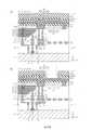
圖4至圖9係顯示第1實施形態之半導體裝置之製造方法之剖視圖。本實施形態之半導體裝置如後文所述,藉由將包含複數個陣列晶片1之陣列晶圓W1、與包含複數個電路晶片2之電路晶圓W2貼合而製造。4 to 9 are cross-sectional views showing the method of manufacturing the semiconductor device according to the first embodiment. The semiconductor device of this embodiment is manufactured by laminating an array wafer W1 including a plurality of
首先,準備基板12,於基板12內形成井區域12a(圖4(a))。圖4(a)顯示基板12內之井區域12a與其他區域12b。接著,於基板12上形成記憶胞陣列11、層間絕緣膜13、通孔插塞45、通孔插塞44、配線層43、通孔插塞42、金屬焊墊41等(圖4(a))。圖4(a)進而顯示記憶胞陣列11所含之字元線WL、絕緣層51、柱狀部CL、階差構造部21等。例如,複數個通孔插塞45於層間絕緣膜13內形成於基板12(井區域12a)上。如此,製造陣列晶圓W1。圖4(a)顯示陣列晶圓W1之上表面S1。First, the
接著,準備基板15,於基板15上形成層間絕緣膜14、電晶體31、閘極電極32、接觸插塞33、配線層34、通孔插塞35、配線層36、通孔插塞37、金屬焊墊38等(圖4(b))。如此,製造電路晶圓W2。圖4(b)顯示電路晶圓W2之上表面S2。Next, the
接著,將陣列晶圓W1與電路晶圓W2貼合(圖5(a))。具體而言,將基板12與基板15介隔記憶胞陣列11、層間絕緣膜13、層間絕緣膜14、電晶體31、通孔插塞45等貼合。圖5(a)中,使陣列晶圓W1之上下方向反轉,將陣列晶圓W1貼合於電路晶圓W2。其結果,將基板12配置於基板15之上方。於該貼合步驟中,層間絕緣膜13與層間絕緣膜14藉由機械壓力而接著,金屬焊墊41與金屬焊墊38藉由退火而接合。Next, the array wafer W1 and the circuit wafer W2 are bonded together ( FIG. 5( a )). Specifically, the
接著,藉由濕蝕刻將基板12薄膜化(圖5(b))。其結果,基板12之厚度變薄。圖5(b)中,基板12內之井區域12a於薄膜化後仍殘留,基板12內之其他區域12b藉由薄膜化而去除。Next, the
接著,於基板12上形成絕緣膜46(圖6(a))。接著,藉由RIE(Reactive Ion Etching:反應離子蝕刻)蝕刻絕緣膜46及基板12(圖6(b))。其結果,於絕緣膜46及基板12內形成開口部H1,於開口部H1內,層間絕緣膜13與上述複數個通孔插塞45露出。再者,於絕緣膜46及基板12內形成開口部H2,於開口部H2內,層間絕緣膜13露出。本實施形態之開口部H2為元件分離槽。圖6(b)之步驟中,藉由上述RIE同時形成開口部H1與開口部H2。開口部H1為第1開口部之例。開口部H2為與第1開口部不同之第2開口部之例。絕緣膜46為第1膜之例。Next, an insulating
接著,於基板12之整面形成絕緣膜47(圖7(a))。其結果,於絕緣膜46、基板12、層間絕緣膜13、及通孔插塞45之表面形成絕緣膜47。具體而言,開口部H1之側面及底面由絕緣膜47覆蓋,開口部H2由絕緣膜47填滿。本實施形態中,以圖7(a)之步驟,於開口部H2內之絕緣膜47內形成氣隙AG。接著,於基板12之整面形成抗蝕劑層71,自開口部H1之底面去除抗蝕劑層71(圖7(a))。Next, an insulating
接著,使用抗蝕劑層71作為遮罩,藉由RIE蝕刻絕緣膜47(圖7(b))。其結果,自開口部H1之底面去除絕緣膜47,於開口部H1內,層間絕緣膜13與上述複數個通孔插塞45再次露出。再者,將絕緣膜47加工成包含以下三部分之形狀,上述三部分指開口部H1之側面之側方部47a、絕緣膜46之上表面之上方側47b、及開口部H2內之埋入部47c。本實施形態中,側方部47a作為側壁絕緣膜發揮功能,埋入膜47c作為元件分離絕緣膜發揮功能。如此,根據本實施形態,可同時形成側壁絕緣膜與元件分離絕緣膜。絕緣膜47為第2膜之例。Next, using the resist
接著,於基板12之整面,形成作為金屬配線48之材料之金屬配線層48(圖8(a))。其結果,於絕緣膜47、層間絕緣膜13及通孔插塞45之表面形成金屬配線層48。具體而言,開口部H1之側面介隔絕緣膜47由金屬配線層48覆蓋,開口部H1之底面由金屬配線層48覆蓋。金屬配線層48例如為包含Al層之金屬層。接著,於基板12之整面形成抗蝕劑層72,其後去除抗蝕劑層72之一部分(圖8(a))。Next, the
接著,使用抗蝕劑層72作為遮罩,藉由RIE蝕刻金屬配線層48(圖8(b))。其結果,金屬配線層48被加工成包含開口部H1之底面之上方部48a、開口部H1之側面之側方部48b、及絕緣膜47之上表面之上方部48c之金屬配線48。因上方部48a形成於上述複數個通孔插塞45上,故金屬配線48電性連接於該等通孔插塞45。因本實施形態之上方部48a、側方部48b及上方部48c由相同之金屬配線層48同時形成,故可由相同材料(例如鋁)形成。本實施形態之上方部48a、側方部48b及上方部48c形成連續之1條配線。Next, using the resist
接著,於基板12之整面,依序形成鈍化膜49之絕緣膜49a、49b、49c(圖9(a))。其結果,於絕緣膜47及金屬配線48之表面形成鈍化膜49。本實施形態之鈍化膜49包含介隔絕緣膜47(側方部47a)與金屬配線48(側方部48a)形成於開口部H1內之部分。Next, the insulating
接著,去除上方部48c之上表面之鈍化膜49之一部分(圖9(b))。其結果,於鈍化膜49內形成開口部P,於開口部P內,上方部48c之上表面露出。於開口部P內露出之上方部48c作為接合墊發揮功能。因此,本實施形態之金屬配線48包含與通孔插塞45相接之部分、及作為接合墊發揮功能之部分之兩者。Next, a part of the
其後,藉由切割將陣列晶圓W1及電路晶圓W2切斷成複數個晶片。該等晶片以各晶片包含1個陣列晶片1與1個電路晶片2之方式被切斷。如此,製造圖1之半導體裝置。Thereafter, the array wafer W1 and the circuit wafer W2 are cut into a plurality of chips by dicing. These chips are cut so that each chip includes one
如以上所述,本實施形態之金屬配線48包含設置於通孔插塞45上之上方部48a、及包含接合墊之上方部48c。因此,根據本實施形態,可以適宜之態樣將接合墊電性連接於通孔插塞45。例如,可不使用如比較例之通孔插塞61而將接合墊電性連接於通孔插塞45,或可減少接合墊與通孔插塞45間之電阻。藉此,可削減半導體裝置之製造步驟數、製造成本。As mentioned above, the
以上,已說明若干實施形態,但該等實施形態僅作為例而提示,並非旨在限定發明範圍者。本說明書中說明之新穎之裝置及方法可以其他各種形態實施。又,對於本說明書中說明之裝置及方法之形態,可於不脫離發明主旨之範圍內進行各種省略、置換、變更。隨附之專利申請範圍及與其均等之範圍旨在包含發明範圍或主旨所含之此種形態或變化例。Although some embodiments have been described above, these embodiments are presented as examples and are not intended to limit the scope of the invention. The novel devices and methods described in this specification can be implemented in other various forms. In addition, various omissions, substitutions, and changes can be made in the form of the apparatus and method described in this specification without departing from the gist of the invention. The scope of the attached patent application and its equivalent scope are intended to cover such forms or modifications included in the scope or spirit of the invention.
[相關申請案] 本申請案享有以日本專利申請案第2020-156645號(申請日:2020年9月17日)為基礎申請案之優先權。本申請案藉由參照該基礎申請案而包含基礎申請案之所有內容。[Related applications] This application enjoys the priority of the basic application based on Japanese Patent Application No. 2020-156645 (filing date: September 17, 2020). This application incorporates all the contents of the basic application by referring to this basic application.
1:陣列晶片 2:電路晶片 11:記憶胞陣列 12:基板 12a:井區域 12b:其他區域 13:層間絕緣膜 14:層間絕緣膜 15:基板 21:階差構造部 22:接觸插塞 23:通孔插塞 24:通孔插塞 31:電晶體 32:閘極電極 33:接觸插塞 34:配線層 35:通孔插塞 36:配線層 37:通孔插塞 38:金屬焊墊 41:金屬焊墊 42:通孔插塞 43:配線層 44:通孔插塞 45:通孔插塞 46:絕緣膜 47:絕緣膜 47a:側方部 47b:上方部 47c:埋入部 48:金屬配線/金屬配線層 48a:上方部 48b:側方部 48c:上方部 49:鈍化膜 49a:絕緣膜 49b:絕緣膜 49c:絕緣膜 51:絕緣層 52:記憶體絕緣膜 52a:阻擋絕緣膜 52b:電荷蓄積層 52c:穿隧絕緣膜 53:通道半導體層 54:芯絕緣膜 55:半導體層 56:半導體層 61:通孔插塞 71:抗蝕劑層 72:抗蝕劑層 AG:氣隙 BL:位元線 CL:柱狀部 H1:開口部 H2:開口部 P:開口部 S:貼合面 S1:上表面 S2:上表面 WL:字元線 WI:字元配線層 W1:陣列晶圓 W2:電路晶圓1: array chip 2: circuit chip 11: Memory cell array 12: Substrate 12a: Well area 12b: Other areas 13: Interlayer insulating film 14: Interlayer insulating film 15: Substrate 21: Step structure department 22: Contact plug 23: Through hole plug 24: Through hole plug 31: Transistor 32: Gate electrode 33: contact plug 34: wiring layer 35: Through hole plug 36: wiring layer 37: Through hole plug 38: Metal pad 41: Metal pad 42: Through hole plug 43: Wiring layer 44: Through hole plug 45: Through hole plug 46: insulating film 47: insulating film 47a: side part 47b: upper part 47c: embedded part 48: Metal wiring/metal wiring layer 48a: upper part 48b: side part 48c: upper part 49: Passivation film 49a: insulating film 49b: insulating film 49c: insulating film 51: Insulation layer 52:Memory insulating film 52a: barrier insulating film 52b: Charge storage layer 52c: tunnel insulating film 53: Channel semiconductor layer 54: core insulating film 55: Semiconductor layer 56: Semiconductor layer 61: Through hole plug 71: resist layer 72: Resist layer AG: air gap BL: bit line CL: columnar part H1: opening H2: opening P: opening S: Fitting surface S1: upper surface S2: upper surface WL: character line WI: character wiring layer W1: array wafer W2: circuit wafer
圖1係顯示第1實施形態之半導體裝置之構造之剖視圖。 圖2係顯示第1實施形態之各柱狀部之構造之剖視圖。 圖3(a)、(b)係用以比較第1實施形態之半導體裝置與其之比較例之半導體裝置之剖視圖。 圖4(a)~9(b)係顯示第1實施形態之半導體裝置之製造方法之剖視圖。FIG. 1 is a cross-sectional view showing the structure of a semiconductor device according to a first embodiment. Fig. 2 is a cross-sectional view showing the structure of each columnar portion in the first embodiment. 3( a ) and ( b ) are sectional views for comparing the semiconductor device of the first embodiment and the semiconductor device of the comparative example. 4(a) to 9(b) are cross-sectional views showing the manufacturing method of the semiconductor device according to the first embodiment.
1:陣列晶片1: array chip
2:電路晶片2: circuit chip
11:記憶胞陣列11: Memory cell array
12:基板12: Substrate
12a:井區域12a: Well area
13:層間絕緣膜13: Interlayer insulating film
14:層間絕緣膜14: Interlayer insulating film
15:基板15: Substrate
21:階差構造部21: Step structure department
22:接觸插塞22: Contact plug
23:通孔插塞23: Through hole plug
24:通孔插塞24: Through hole plug
31:電晶體31: Transistor
32:閘極電極32: Gate electrode
33:接觸插塞33: contact plug
34:配線層34: wiring layer
35:通孔插塞35: Through hole plug
36:配線層36: wiring layer
37:通孔插塞37: Through hole plug
38:金屬焊墊38: Metal pad
41:金屬焊墊41: Metal pad
42:通孔插塞42: Through hole plug
43:配線層43: Wiring layer
44:通孔插塞44: Through hole plug
45:通孔插塞45: Through hole plug
46:絕緣膜46: insulating film
47:絕緣膜47: insulating film
47a:側方部47a: side part
47b:上方部47b: upper part
47c:埋入部47c: embedded part
48:金屬配線/金屬配線層48: Metal wiring/metal wiring layer
48a:上方部48a: upper part
48b:側方部48b: side part
48c:上方部48c: upper part
49:鈍化膜49: Passivation film
49a:絕緣膜49a: insulating film
49b:絕緣膜49b: insulating film
49c:絕緣膜49c: insulating film
51:絕緣層51: Insulation layer
52:記憶體絕緣膜52:Memory insulating film
53:通道半導體層53: Channel semiconductor layer
54:芯絕緣膜54: core insulating film
55:半導體層55: Semiconductor layer
56:半導體層56: Semiconductor layer
AG:氣隙AG: air gap
BL:位元線BL: bit line
CL:柱狀部CL: columnar part
P:開口部P: opening
S:貼合面S: Fitting surface
WL:字元線WL: character line
WI:字元配線層WI: character wiring layer
Claims (12)
Translated fromChineseApplications Claiming Priority (2)
| Application Number | Priority Date | Filing Date | Title |
|---|---|---|---|
| JP2020-156645 | 2020-09-17 | ||
| JP2020156645AJP2022050185A (en) | 2020-09-17 | 2020-09-17 | Semiconductor devices and their manufacturing methods |
Publications (2)
| Publication Number | Publication Date |
|---|---|
| TW202213554A TW202213554A (en) | 2022-04-01 |
| TWI782400Btrue TWI782400B (en) | 2022-11-01 |
Family
ID=80627003
Family Applications (1)
| Application Number | Title | Priority Date | Filing Date |
|---|---|---|---|
| TW110102842ATWI782400B (en) | 2020-09-17 | 2021-01-26 | Semiconductor device and method of manufacturing the same |
Country Status (4)
| Country | Link |
|---|---|
| US (2) | US11562976B2 (en) |
| JP (1) | JP2022050185A (en) |
| CN (1) | CN114203656A (en) |
| TW (1) | TWI782400B (en) |
Families Citing this family (5)
| Publication number | Priority date | Publication date | Assignee | Title |
|---|---|---|---|---|
| JP2022044428A (en)* | 2020-09-07 | 2022-03-17 | キオクシア株式会社 | Manufacturing method of semiconductor storage device and semiconductor storage device |
| KR20220053733A (en)* | 2020-10-22 | 2022-05-02 | 삼성전자주식회사 | Semiconductor memory device, electronic system including the same, and method for fabricating the same |
| JP2022128770A (en)* | 2021-02-24 | 2022-09-05 | キオクシア株式会社 | semiconductor storage device |
| JP7631049B2 (en)* | 2021-03-16 | 2025-02-18 | キオクシア株式会社 | Semiconductor memory device and method for manufacturing the same |
| EP4501627A1 (en) | 2022-03-25 | 2025-02-05 | Ajinomoto Co., Inc. | Resin sheet and production method therefor |
Citations (3)
| Publication number | Priority date | Publication date | Assignee | Title |
|---|---|---|---|---|
| US20160079164A1 (en)* | 2014-09-12 | 2016-03-17 | Kabushiki Kaisha Toshiba | Semiconductor memory device and method for manufacturing same |
| US20200286990A1 (en)* | 2019-03-07 | 2020-09-10 | Toshiba Memory Corporation | Semiconductor device and manufacturing method of semiconductor device |
| TW202034493A (en)* | 2019-03-11 | 2020-09-16 | 日商東芝記憶體股份有限公司 | Semiconductor device and method of manufacturing the same |
Family Cites Families (5)
| Publication number | Priority date | Publication date | Assignee | Title |
|---|---|---|---|---|
| JP5376916B2 (en) | 2008-11-26 | 2013-12-25 | ルネサスエレクトロニクス株式会社 | Manufacturing method of semiconductor device |
| JP2020141100A (en)* | 2019-03-01 | 2020-09-03 | キオクシア株式会社 | Semiconductor devices and their manufacturing methods |
| JP2020145231A (en)* | 2019-03-04 | 2020-09-10 | キオクシア株式会社 | Semiconductor device and manufacturing method thereof |
| US11211370B2 (en)* | 2020-01-28 | 2021-12-28 | Sandisk Technologies Llc | Bonded assembly with vertical power and control signal connection adjacent to sense amplifier regions and methods of forming the same |
| US11444039B2 (en)* | 2020-05-29 | 2022-09-13 | Sandisk Technologies Llc | Semiconductor die including diffusion barrier layers embedding bonding pads and methods of forming the same |
- 2020
- 2020-09-17JPJP2020156645Apatent/JP2022050185A/enactivePending
- 2021
- 2021-01-26TWTW110102842Apatent/TWI782400B/enactive
- 2021-01-28CNCN202110117503.7Apatent/CN114203656A/enactivePending
- 2021-03-02USUS17/190,006patent/US11562976B2/enactiveActive
- 2022
- 2022-12-23USUS18/145,979patent/US12057422B2/enactiveActive
Patent Citations (3)
| Publication number | Priority date | Publication date | Assignee | Title |
|---|---|---|---|---|
| US20160079164A1 (en)* | 2014-09-12 | 2016-03-17 | Kabushiki Kaisha Toshiba | Semiconductor memory device and method for manufacturing same |
| US20200286990A1 (en)* | 2019-03-07 | 2020-09-10 | Toshiba Memory Corporation | Semiconductor device and manufacturing method of semiconductor device |
| TW202034493A (en)* | 2019-03-11 | 2020-09-16 | 日商東芝記憶體股份有限公司 | Semiconductor device and method of manufacturing the same |
Also Published As
| Publication number | Publication date |
|---|---|
| US11562976B2 (en) | 2023-01-24 |
| US20220084970A1 (en) | 2022-03-17 |
| JP2022050185A (en) | 2022-03-30 |
| TW202213554A (en) | 2022-04-01 |
| CN114203656A (en) | 2022-03-18 |
| US12057422B2 (en) | 2024-08-06 |
| US20230129339A1 (en) | 2023-04-27 |
Similar Documents
| Publication | Publication Date | Title |
|---|---|---|
| TWI782794B (en) | semiconductor device | |
| US20250132276A1 (en) | Semiconductor device | |
| TWI711164B (en) | Semiconductor device and manufacturing method thereof | |
| TWI782400B (en) | Semiconductor device and method of manufacturing the same | |
| TWI725489B (en) | Semiconductor device and manufacturing method thereof | |
| TWI776616B (en) | Semiconductor device and method of manufacturing the same | |
| US11594514B2 (en) | Semiconductor device and method of manufacturing the same | |
| TWI770401B (en) | Semiconductor device and method of manufacturing the same | |
| TW202135240A (en) | Semiconductor device and manufacturing method thereof | |
| US11756909B2 (en) | Semiconductor storage device and method of manufacturing semiconductor storage device | |
| TWI787842B (en) | Semiconductor device and manufacturing method thereof | |
| TWI776181B (en) | Semiconductor device and method for manufacturing the same | |
| TWI849321B (en) | Semiconductor memory device and method for manufacturing the same | |
| TWI858315B (en) | Semiconductor devices | |
| JP2024129670A (en) | Semiconductor device and its manufacturing method | |
| JP2023177154A (en) | Semiconductor device and method for manufacturing the same |