TWI781445B - High-power vcsel - Google Patents
High-power vcselDownload PDFInfo
- Publication number
- TWI781445B TWI781445BTW109132787ATW109132787ATWI781445BTW I781445 BTWI781445 BTW I781445BTW 109132787 ATW109132787 ATW 109132787ATW 109132787 ATW109132787 ATW 109132787ATW I781445 BTWI781445 BTW I781445B
- Authority
- TW
- Taiwan
- Prior art keywords
- layer
- epitaxial
- type
- region
- laser diode
- Prior art date
Links
- 125000006850spacer groupChemical group0.000claimsdescription61
- 238000006243chemical reactionMethods0.000claimsdescription31
- 239000000463materialSubstances0.000claimsdescription19
- 239000000758substrateSubstances0.000claimsdescription14
- 229910001218Gallium arsenideInorganic materials0.000claimsdescription6
- 229910000530Gallium indium arsenideInorganic materials0.000claimsdescription3
- 239000010410layerSubstances0.000description359
- 238000010586diagramMethods0.000description8
- 238000002310reflectometryMethods0.000description6
- 238000000407epitaxyMethods0.000description4
- 230000003287optical effectEffects0.000description3
- 238000009826distributionMethods0.000description2
- 230000000694effectsEffects0.000description2
- 230000031700light absorptionEffects0.000description2
- 239000002344surface layerSubstances0.000description2
- 230000005641tunnelingEffects0.000description2
- VZSRBBMJRBPUNF-UHFFFAOYSA-N2-(2,3-dihydro-1H-inden-2-ylamino)-N-[3-oxo-3-(2,4,6,7-tetrahydrotriazolo[4,5-c]pyridin-5-yl)propyl]pyrimidine-5-carboxamideChemical compoundC1C(CC2=CC=CC=C12)NC1=NC=C(C=N1)C(=O)NCCC(N1CC2=C(CC1)NN=N2)=OVZSRBBMJRBPUNF-UHFFFAOYSA-N0.000description1
- YLZOPXRUQYQQID-UHFFFAOYSA-N3-(2,4,6,7-tetrahydrotriazolo[4,5-c]pyridin-5-yl)-1-[4-[2-[[3-(trifluoromethoxy)phenyl]methylamino]pyrimidin-5-yl]piperazin-1-yl]propan-1-oneChemical compoundN1N=NC=2CN(CCC=21)CCC(=O)N1CCN(CC1)C=1C=NC(=NC=1)NCC1=CC(=CC=C1)OC(F)(F)FYLZOPXRUQYQQID-UHFFFAOYSA-N0.000description1
- NIPNSKYNPDTRPC-UHFFFAOYSA-NN-[2-oxo-2-(2,4,6,7-tetrahydrotriazolo[4,5-c]pyridin-5-yl)ethyl]-2-[[3-(trifluoromethoxy)phenyl]methylamino]pyrimidine-5-carboxamideChemical compoundO=C(CNC(=O)C=1C=NC(=NC=1)NCC1=CC(=CC=C1)OC(F)(F)F)N1CC2=C(CC1)NN=N2NIPNSKYNPDTRPC-UHFFFAOYSA-N0.000description1
- AFCARXCZXQIEQB-UHFFFAOYSA-NN-[3-oxo-3-(2,4,6,7-tetrahydrotriazolo[4,5-c]pyridin-5-yl)propyl]-2-[[3-(trifluoromethoxy)phenyl]methylamino]pyrimidine-5-carboxamideChemical compoundO=C(CCNC(=O)C=1C=NC(=NC=1)NCC1=CC(=CC=C1)OC(F)(F)F)N1CC2=C(CC1)NN=N2AFCARXCZXQIEQB-UHFFFAOYSA-N0.000description1
- 238000010521absorption reactionMethods0.000description1
- QVGXLLKOCUKJST-UHFFFAOYSA-Natomic oxygenChemical compound[O]QVGXLLKOCUKJST-UHFFFAOYSA-N0.000description1
- 230000002238attenuated effectEffects0.000description1
- 239000000969carrierSubstances0.000description1
- 230000008859changeEffects0.000description1
- 238000004891communicationMethods0.000description1
- 239000013078crystalSubstances0.000description1
- 239000006185dispersionSubstances0.000description1
- 238000005516engineering processMethods0.000description1
- 238000000605extractionMethods0.000description1
- 230000017525heat dissipationEffects0.000description1
- 238000004519manufacturing processMethods0.000description1
- 238000000034methodMethods0.000description1
- 230000004048modificationEffects0.000description1
- 238000012986modificationMethods0.000description1
- 230000005693optoelectronicsEffects0.000description1
- 229910052760oxygenInorganic materials0.000description1
- 239000001301oxygenSubstances0.000description1
- 210000004508polar bodyAnatomy0.000description1
- 239000002356single layerSubstances0.000description1
- 230000007480spreadingEffects0.000description1
- 238000003892spreadingMethods0.000description1
- 230000009466transformationEffects0.000description1
- 238000000844transformationMethods0.000description1
- 230000007704transitionEffects0.000description1
Images


Classifications
- H—ELECTRICITY
- H01—ELECTRIC ELEMENTS
- H01S—DEVICES USING THE PROCESS OF LIGHT AMPLIFICATION BY STIMULATED EMISSION OF RADIATION [LASER] TO AMPLIFY OR GENERATE LIGHT; DEVICES USING STIMULATED EMISSION OF ELECTROMAGNETIC RADIATION IN WAVE RANGES OTHER THAN OPTICAL
- H01S5/00—Semiconductor lasers
- H01S5/10—Construction or shape of the optical resonator, e.g. extended or external cavity, coupled cavities, bent-guide, varying width, thickness or composition of the active region
- H01S5/18—Surface-emitting [SE] lasers, e.g. having both horizontal and vertical cavities
- H01S5/183—Surface-emitting [SE] lasers, e.g. having both horizontal and vertical cavities having only vertical cavities, e.g. vertical cavity surface-emitting lasers [VCSEL]
- H01S5/18361—Structure of the reflectors, e.g. hybrid mirrors
- H—ELECTRICITY
- H01—ELECTRIC ELEMENTS
- H01S—DEVICES USING THE PROCESS OF LIGHT AMPLIFICATION BY STIMULATED EMISSION OF RADIATION [LASER] TO AMPLIFY OR GENERATE LIGHT; DEVICES USING STIMULATED EMISSION OF ELECTROMAGNETIC RADIATION IN WAVE RANGES OTHER THAN OPTICAL
- H01S5/00—Semiconductor lasers
- H01S5/10—Construction or shape of the optical resonator, e.g. extended or external cavity, coupled cavities, bent-guide, varying width, thickness or composition of the active region
- H01S5/18—Surface-emitting [SE] lasers, e.g. having both horizontal and vertical cavities
- H01S5/183—Surface-emitting [SE] lasers, e.g. having both horizontal and vertical cavities having only vertical cavities, e.g. vertical cavity surface-emitting lasers [VCSEL]
- H01S5/18305—Surface-emitting [SE] lasers, e.g. having both horizontal and vertical cavities having only vertical cavities, e.g. vertical cavity surface-emitting lasers [VCSEL] with emission through the substrate, i.e. bottom emission
- H—ELECTRICITY
- H01—ELECTRIC ELEMENTS
- H01S—DEVICES USING THE PROCESS OF LIGHT AMPLIFICATION BY STIMULATED EMISSION OF RADIATION [LASER] TO AMPLIFY OR GENERATE LIGHT; DEVICES USING STIMULATED EMISSION OF ELECTROMAGNETIC RADIATION IN WAVE RANGES OTHER THAN OPTICAL
- H01S5/00—Semiconductor lasers
- H01S5/10—Construction or shape of the optical resonator, e.g. extended or external cavity, coupled cavities, bent-guide, varying width, thickness or composition of the active region
- H01S5/18—Surface-emitting [SE] lasers, e.g. having both horizontal and vertical cavities
- H01S5/183—Surface-emitting [SE] lasers, e.g. having both horizontal and vertical cavities having only vertical cavities, e.g. vertical cavity surface-emitting lasers [VCSEL]
- H01S5/18308—Surface-emitting [SE] lasers, e.g. having both horizontal and vertical cavities having only vertical cavities, e.g. vertical cavity surface-emitting lasers [VCSEL] having a special structure for lateral current or light confinement
- H01S5/18311—Surface-emitting [SE] lasers, e.g. having both horizontal and vertical cavities having only vertical cavities, e.g. vertical cavity surface-emitting lasers [VCSEL] having a special structure for lateral current or light confinement using selective oxidation
- H—ELECTRICITY
- H01—ELECTRIC ELEMENTS
- H01S—DEVICES USING THE PROCESS OF LIGHT AMPLIFICATION BY STIMULATED EMISSION OF RADIATION [LASER] TO AMPLIFY OR GENERATE LIGHT; DEVICES USING STIMULATED EMISSION OF ELECTROMAGNETIC RADIATION IN WAVE RANGES OTHER THAN OPTICAL
- H01S5/00—Semiconductor lasers
- H01S5/10—Construction or shape of the optical resonator, e.g. extended or external cavity, coupled cavities, bent-guide, varying width, thickness or composition of the active region
- H01S5/18—Surface-emitting [SE] lasers, e.g. having both horizontal and vertical cavities
- H01S5/183—Surface-emitting [SE] lasers, e.g. having both horizontal and vertical cavities having only vertical cavities, e.g. vertical cavity surface-emitting lasers [VCSEL]
- H01S5/18308—Surface-emitting [SE] lasers, e.g. having both horizontal and vertical cavities having only vertical cavities, e.g. vertical cavity surface-emitting lasers [VCSEL] having a special structure for lateral current or light confinement
- H01S5/18322—Position of the structure
- H—ELECTRICITY
- H01—ELECTRIC ELEMENTS
- H01S—DEVICES USING THE PROCESS OF LIGHT AMPLIFICATION BY STIMULATED EMISSION OF RADIATION [LASER] TO AMPLIFY OR GENERATE LIGHT; DEVICES USING STIMULATED EMISSION OF ELECTROMAGNETIC RADIATION IN WAVE RANGES OTHER THAN OPTICAL
- H01S5/00—Semiconductor lasers
- H01S5/30—Structure or shape of the active region; Materials used for the active region
- H01S5/305—Structure or shape of the active region; Materials used for the active region characterised by the doping materials used in the laser structure
- H01S5/3095—Tunnel junction
- H—ELECTRICITY
- H01—ELECTRIC ELEMENTS
- H01S—DEVICES USING THE PROCESS OF LIGHT AMPLIFICATION BY STIMULATED EMISSION OF RADIATION [LASER] TO AMPLIFY OR GENERATE LIGHT; DEVICES USING STIMULATED EMISSION OF ELECTROMAGNETIC RADIATION IN WAVE RANGES OTHER THAN OPTICAL
- H01S5/00—Semiconductor lasers
- H01S5/0014—Measuring characteristics or properties thereof
- H—ELECTRICITY
- H01—ELECTRIC ELEMENTS
- H01S—DEVICES USING THE PROCESS OF LIGHT AMPLIFICATION BY STIMULATED EMISSION OF RADIATION [LASER] TO AMPLIFY OR GENERATE LIGHT; DEVICES USING STIMULATED EMISSION OF ELECTROMAGNETIC RADIATION IN WAVE RANGES OTHER THAN OPTICAL
- H01S5/00—Semiconductor lasers
- H01S5/10—Construction or shape of the optical resonator, e.g. extended or external cavity, coupled cavities, bent-guide, varying width, thickness or composition of the active region
- H01S5/18—Surface-emitting [SE] lasers, e.g. having both horizontal and vertical cavities
- H01S5/183—Surface-emitting [SE] lasers, e.g. having both horizontal and vertical cavities having only vertical cavities, e.g. vertical cavity surface-emitting lasers [VCSEL]
- H01S5/18308—Surface-emitting [SE] lasers, e.g. having both horizontal and vertical cavities having only vertical cavities, e.g. vertical cavity surface-emitting lasers [VCSEL] having a special structure for lateral current or light confinement
- H01S5/18322—Position of the structure
- H01S5/18325—Between active layer and substrate
- H—ELECTRICITY
- H01—ELECTRIC ELEMENTS
- H01S—DEVICES USING THE PROCESS OF LIGHT AMPLIFICATION BY STIMULATED EMISSION OF RADIATION [LASER] TO AMPLIFY OR GENERATE LIGHT; DEVICES USING STIMULATED EMISSION OF ELECTROMAGNETIC RADIATION IN WAVE RANGES OTHER THAN OPTICAL
- H01S5/00—Semiconductor lasers
- H01S5/10—Construction or shape of the optical resonator, e.g. extended or external cavity, coupled cavities, bent-guide, varying width, thickness or composition of the active region
- H01S5/18—Surface-emitting [SE] lasers, e.g. having both horizontal and vertical cavities
- H01S5/183—Surface-emitting [SE] lasers, e.g. having both horizontal and vertical cavities having only vertical cavities, e.g. vertical cavity surface-emitting lasers [VCSEL]
- H01S5/18308—Surface-emitting [SE] lasers, e.g. having both horizontal and vertical cavities having only vertical cavities, e.g. vertical cavity surface-emitting lasers [VCSEL] having a special structure for lateral current or light confinement
- H01S5/18322—Position of the structure
- H01S5/1833—Position of the structure with more than one structure
- H01S5/18333—Position of the structure with more than one structure only above the active layer
- H—ELECTRICITY
- H01—ELECTRIC ELEMENTS
- H01S—DEVICES USING THE PROCESS OF LIGHT AMPLIFICATION BY STIMULATED EMISSION OF RADIATION [LASER] TO AMPLIFY OR GENERATE LIGHT; DEVICES USING STIMULATED EMISSION OF ELECTROMAGNETIC RADIATION IN WAVE RANGES OTHER THAN OPTICAL
- H01S5/00—Semiconductor lasers
- H01S5/10—Construction or shape of the optical resonator, e.g. extended or external cavity, coupled cavities, bent-guide, varying width, thickness or composition of the active region
- H01S5/18—Surface-emitting [SE] lasers, e.g. having both horizontal and vertical cavities
- H01S5/183—Surface-emitting [SE] lasers, e.g. having both horizontal and vertical cavities having only vertical cavities, e.g. vertical cavity surface-emitting lasers [VCSEL]
- H01S5/18397—Plurality of active layers vertically stacked in a cavity for multi-wavelength emission
- H—ELECTRICITY
- H01—ELECTRIC ELEMENTS
- H01S—DEVICES USING THE PROCESS OF LIGHT AMPLIFICATION BY STIMULATED EMISSION OF RADIATION [LASER] TO AMPLIFY OR GENERATE LIGHT; DEVICES USING STIMULATED EMISSION OF ELECTROMAGNETIC RADIATION IN WAVE RANGES OTHER THAN OPTICAL
- H01S5/00—Semiconductor lasers
- H01S5/30—Structure or shape of the active region; Materials used for the active region
- H01S5/305—Structure or shape of the active region; Materials used for the active region characterised by the doping materials used in the laser structure
- H01S5/3054—Structure or shape of the active region; Materials used for the active region characterised by the doping materials used in the laser structure p-doping
Landscapes
- Physics & Mathematics (AREA)
- Condensed Matter Physics & Semiconductors (AREA)
- General Physics & Mathematics (AREA)
- Electromagnetism (AREA)
- Optics & Photonics (AREA)
- Semiconductor Lasers (AREA)
- Superconductors And Manufacturing Methods Therefor (AREA)
Abstract
Description
Translated fromChinese一種VCSEL,尤其是一種具有PN轉換結構的高功率VCSEL,適合應用於距離感測、3D感測、光達與紅外線照明等技術領域。A VCSEL, especially a high-power VCSEL with a PN switching structure, suitable forIt is used in technical fields such as distance sensing, 3D sensing, lidar and infrared lighting.
垂直共振腔表面放射雷射二極體(Vertical Cavity Surface EmittingLaser Diode, VCSEL)是雷射元件的一種,其可以用來做為3D感測、光通訊或紅外線照明的光源。根據雷射光發出的方向,垂直共振腔表面放射雷射二極體可區分為正面出光型(上DBR層的總反射率小於下DBR層的總反射率)與背面出光型(上DBR層的總反射率大於下DBR層的總反射率)。Vertical Cavity Surface Emitting Laser Diode (Vertical Cavity Surface EmittingLaser Diode, VCSEL) is a kind of laser component, which can be used as a light source for 3D sensing, optical communication or infrared lighting. According to the direction in which the laser light is emitted, the laser diodes emitting on the surface of the vertical resonator can be divided into front-emitting type (the total reflectivity of the upper DBR layer is smaller than that of the lower DBR layer) and back-emitting type (the total reflectivity of the upper DBR layer The reflectivity is greater than the total reflectivity of the lower DBR layer).
VCSEL的製作是在基板之上磊晶成長多層結構而成,多層結構中包含下磊晶區、主動區與上磊晶區。The production of VCSEL is formed by growing a multilayer structure by epitaxial growth on the substrate, and the multilayer structureIncluding the lower epitaxy region, the active region and the upper epitaxy region.
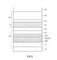
參圖1,下磊晶區包含下DBR層20’與下間隔層30’,上磊晶區包含上間隔層34’與上DBR層40’;主動區32’介於下磊晶區與上磊晶區之間。下磊晶區與上磊晶區中分別具有多層的N型磊晶層與多層的P型磊晶層,或分別具有多層的P型磊晶層與多層的N型磊晶層。下DBR層20’或上DBR層40’的設置層數通常多達數十層。Referring to Fig. 1, the lower epitaxial region includes the lower DBR layer 20' and the lower spacer layer 30', and the upper epitaxial region includesThe upper spacer layer 34' and the upper DBR layer 40'; the active region 32' is between the lower epitaxy region and the upper epitaxy region. The lower epitaxial region and the upper epitaxial region respectively have multiple layers of N-type epitaxial layers and multiple layers of P-type epitaxial layers, or respectively have multiple layers of P-type epitaxial layers and multiple layers of N-type epitaxial layers. The number of layers of the lower DBR layer 20' or the upper DBR layer 40' is usually as many as tens of layers.
P型磊晶層與N型磊晶層的多數載子(majority carrier)分別是電洞與電子。由於電洞的有效質量(effective mass)比電子大、遷移率(mobility)比電子低,P型磊晶層材料的電阻不但比N型磊晶層大,且導熱也比N型磊晶層差。此外,由於P型磊晶層材料的電阻較大,電流在通過P型磊晶層時不容易均勻散佈(Current spreading)。The majority carriers of the P-type epitaxial layer and the N-type epitaxial layer are electricholes and electrons. Since the effective mass of the hole is larger than that of the electron and the mobility is lower than that of the electron, the resistance of the P-type epitaxial layer material is not only larger than that of the N-type epitaxial layer, but also the thermal conductivity is worse than that of the N-type epitaxial layer. . In addition, due to the high resistance of the material of the P-type epitaxial layer, the current is not easy to spread uniformly (Current spreading) when passing through the P-type epitaxial layer.
當P型磊晶層與N型磊晶層的摻雜濃度相同時,P型磊晶層對光的吸收會比N型的磊晶層多。P型磊晶層吸收光線後除了會降低主動區的出光效率,也會因吸收光的能量而導致P型磊晶層溫度容易升高。When the doping concentration of the P-type epitaxial layer and the N-type epitaxial layer is the same, the P-type epitaxial layer has the same effect on lightThe absorption will be more than the N-type epitaxial layer. After the P-type epitaxial layer absorbs light, not only will the light extraction efficiency of the active region be reduced, but also the temperature of the P-type epitaxial layer will easily rise due to the energy of the absorbed light.
當下(上)DBR層中的數十層都是P型磊晶層時,則下(上)DBR層20’中的整體電阻偏大,電阻偏大表示功率損耗也大,如此VCSEL的出光功率與光電特性容易受限或甚至衰減。When dozens of layers in the lower (upper) DBR layer are P-type epitaxial layers, the lower (upper) DBRThe overall resistance in the layer 20' is relatively large, which means that the power loss is also large, so the light output power and photoelectric characteristics of the VCSEL are easily limited or even attenuated.
此外,由於電流通過數十層P型磊晶層時電流不容易均勻分佈,如此VCSEL所發射出的雷射光的發散角會較大,或VCSEL的雷射光的光形(beam profile)較不接近所需的特定光形。In addition, because the current is not easy to distribute evenly when the current passes through dozens of P-type epitaxial layers, such asThe divergence angle of the laser light emitted by the VCSEL is larger, or the beam profile of the laser light of the VCSEL is not close to the desired specific beam profile.
P型磊晶層的層數較多,P型磊晶層會吸收較多的光能;因此VCSEL工作時,P型下(上)DBR層的溫度容易偏高,而P型磊晶層的導熱又不佳,難以將主動區的熱能排散。因此VCSEL工作時,主動區的溫度因較難下降而偏高,造成VCSEL的出光功率與光電特性受到限制。The P-type epitaxial layer has more layers, and the P-type epitaxial layer will absorb more light energy; therefore, the VCSELDuring operation, the temperature of the P-type lower (upper) DBR layer tends to be too high, and the heat conduction of the P-type epitaxial layer is not good, so it is difficult to dissipate the heat energy in the active region. Therefore, when the VCSEL is working, the temperature of the active region is relatively high because it is difficult to drop, which limits the output power and photoelectric characteristics of the VCSEL.
通常在下(上)磊晶區設置DBR層以外的磊晶層,或者在主動區增加主動層的設置數目及其他磊晶層,能夠改善或增進VCSEL中的光電特性;不過現有技術中,在P型下(上)磊晶區中所增設的磊晶層須為P型摻雜或未摻雜的磊晶層,因此P型下(上)磊晶區的電阻或光吸收率很可能還會提高。再者,在主動區之上或之下的P型磊晶層的堆疊層數越多,主動區的溫度恐更難降低;因此在下(上)磊晶區設置DBR層以外的磊晶層,VCSEL的出光功率與光電特性反而有進一步降低的風險。Usually the epitaxial layer other than the DBR layer is set in the lower (upper) epitaxial area, or in the active areaIncreasing the number of active layers and other epitaxial layers can improve or enhance the photoelectric characteristics in VCSEL; however, in the prior art, the additional epitaxial layers in the P-type lower (upper) epitaxial region must be P-type doped Or an undoped epitaxial layer, so the resistance or light absorption rate of the P-type lower (upper) epitaxial region is likely to increase. Furthermore, the more stacked layers of P-type epitaxial layers above or below the active region, the more difficult it is to reduce the temperature of the active region; therefore, setting epitaxial layers other than the DBR layer in the lower (upper) epitaxial region, On the contrary, the output power and photoelectric characteristics of VCSEL may be further reduced.
在一實施例,提供一種高功率VCSEL,其主要包括一N型第一磊晶區、一主動區與一第二磊晶區;該N型第一磊晶區位於一基板之上;該主動區係位於該N型第一磊晶區之上,該主動區包含一或複數主動層;該第二磊晶區位於該主動區之上,該第二磊晶區包含一PN轉換結構(PN junction);該PN轉換結構包含至少一P型磊晶層、一穿隧接面層與至少一N型磊晶層,其中該穿隧接面層位於該至少一P型磊晶層與該至少一N型磊晶層之間;其中,該至少一P型磊晶層係靠近於該主動區,且該至少一P型磊晶層是介於該至少一N型磊晶層與該主動區之間。In one embodiment, a high-power VCSEL is provided, which mainly includes an N-type first epitaxialCrystal region, an active region and a second epitaxial region; the N-type first epitaxial region is located on a substrate; the active region is located on the N-type first epitaxial region, and the active region includes one or A plurality of active layers; the second epitaxial region is located on the active region, the second epitaxial region includes a PN transition structure (PN junction); the PN junction structure includes at least one P-type epitaxial layer, a tunnel junction Surface layer and at least one N-type epitaxial layer, wherein the tunnel junction layer is located between the at least one P-type epitaxial layer and the at least one N-type epitaxial layer; wherein, the at least one P-type epitaxial layer is It is close to the active area, and the at least one P-type epitaxial layer is between the at least one N-type epitaxial layer and the active area.
在一實施例,提供一種高功率VCSEL,其包括一第一磊晶區、一主動區與一N型第二磊晶區。該第一磊晶區係位於一基板之上,該第一磊晶區包含一PN轉換結構(PN junction),該PN轉換結構包含至少一P型磊晶層、一穿隧接面層與至少一N型磊晶層,其中該穿隧接面層位於該至少一P型磊晶層與該至少一N型磊晶層之間;該主動區位於該第一磊晶區之上,該主動區包含一或複數主動層;該N型第二磊晶區位於該主動區之上;該至少一P型磊晶層係靠近於該主動區,而該至少一N型磊晶層則靠近於該基板。In one embodiment, a high power VCSEL is provided, which includes a first epitaxial region, an active region and an N-type second epitaxial region. The first epitaxial region is located on a substrate, the first epitaxial region includes a PN junction structure, and the PN junction structure includes at least one P-type epitaxial layer, a tunnel junction layer and at least An N-type epitaxial layer, wherein the tunnel junction layer is located between the at least one P-type epitaxial layer and the at least one N-type epitaxial layer; the active region is located on the first epitaxial region, and the active The region includes one or a plurality of active layers; the N-type second epitaxial region is located on the active region; the at least one P-type epitaxial layer is close to the active region, and the at least one N-type epitaxial layer is close to the active region the substrate.
以下配合圖式及元件符號對本發明的實施方式作更詳細的說明,俾使熟習該項技藝者在研讀本說明書後能據以實施。為便於理解本發明,圖式中僅繪製出雷射二極體的部分結構,並非限制雷射二極體僅由下述結構所構成。圖式中各層之間的厚度比例也非實際比例,應根據實際需要而調整各層的厚度。Embodiments of the present invention will be described in more detail below in conjunction with the drawings and reference numbers,So that those who are familiar with the art can implement it after studying this manual. In order to facilitate the understanding of the present invention, only a part of the structure of the laser diode is drawn in the drawings, and the laser diode is not limited to be composed of only the following structures. The thickness ratio between the layers in the drawing is also not the actual ratio, and the thickness of each layer should be adjusted according to actual needs.
以下描述具體的元件及其排列的例子以簡化本發明。當然這些僅是例子且不該以此限定本發明的範圍。例如,在描述中提及一層於另一層之上時,其可能包括該層與該另一層層直接接觸的實施例,也可能包括兩者之間有其他元件或磊晶層形成而沒有直接接觸的實施例。此外,在不同實施例中可能使用重複的標號及/或符號,這些重複僅為了簡單清楚地敘述一些實施例,不代表所討論的不同實施例及/或結構之間有特定關聯。Specific examples of elements and their arrangements are described below to simplify the present invention. Of course these are onlyare examples and should not be used to limit the scope of the invention. For example, when the description refers to a layer being on top of another layer, it may include embodiments where the layer is in direct contact with the other layer, or may include other elements or epitaxial layers formed therebetween without direct contact. the embodiment. In addition, repeated numbers and/or symbols may be used in different embodiments, and these repetitions are only for the purpose of describing some embodiments simply and clearly, and do not mean that there is a specific relationship between the different embodiments and/or structures discussed.
此外,其中可能用到與空間相關的用詞,像是“在...下方”、“下方”、“較低的”、“上方”、“較高的”及類似的用詞,這些關係詞係為了便於描述圖式中一個(些)元件或特徵與另一個(些)元件或特徵之間的關係。這些空間關係詞包括使用中或操作中的裝置之不同方位,以及圖式中所描述的方位。In addition, space-related terms may be used, such as "below", "beneath","Lower", "above", "higher" and similar terms are used to describe the relationship between one (some) element or feature and another (some) element or feature in the drawings. relation. These spatial relative terms include various orientations of the device in use or operation, as well as the orientations depicted in the drawings.
本發明說明書提供不同的實施例來說明不同實施方式的技術特徵。舉例而言,全文說明書中所指的“一些實施例”意味著在實施例中描述到的特定特徵、結構、或特色至少包含在一實施例中。因此,全文說明書不同地方所出現的片語“在一些實施例中”所指不一定為相同的實施例。The description of the present invention provides different embodiments to illustrate the technical features of different implementations.sign. For example, "some embodiments" referred to throughout the specification means that the specific features, structures, or characteristics described in the embodiments are included in at least one embodiment. Thus, appearances of the phrase "in some embodiments" in various places throughout the specification are not necessarily to the same embodiments.
此外,特定的特徵、結構、或特色可在一或多個的實施例中透過任何合適的方法結合。進一步地,對於在此所使用的用語“包括”、“具有”、“有”、“其中”或前述之變換,這些語意類似於用語“包括”來包含相應的特徵。In addition, specific features, structures, or characteristics may be disclosed in one or more embodimentsAny suitable combination of methods. Further, as for the terms "comprising", "having", "having", "in which" or the aforementioned transformations used herein, these meanings are similar to the term "comprising" to include corresponding features.
此外,”層”可以是單一層或者包含是多層;而一磊晶層的”一部分”可能是該磊晶層的一層或互為相鄰的複數層。In addition, a "layer" can be a single layer or include multiple layers; and a "part" of an epitaxial layerIt may be one layer of the epitaxial layer or a plurality of layers adjacent to each other.
現有技術中,雷射二極體可依據實際需求而選擇性的設置緩衝層,且在一些實例中,緩衝層可與基板在材質是相同的。且緩衝層設置與否,跟以下實施例所欲講述的技術特點與所欲提供的效果並無實質相關,因此為了簡要示例說明,以下實施例僅以具有緩衝層的雷射二極體來做為說明用的示例,而不另贅述沒有設置緩衝層的雷射二極體,也就是以下實施例如置換無緩衝層的雷射二極體也能一體適用。In the prior art, the laser diode can be selectively provided with a buffer layer according to actual needs,And in some examples, the material of the buffer layer and the substrate can be the same. And whether the buffer layer is set or not is not substantially related to the technical characteristics and the effects to be provided in the following embodiments. Therefore, for a brief illustration, the following embodiments only use a laser diode with a buffer layer. It is an example for illustration, and the laser diode without the buffer layer is not further described, that is, the following embodiments can also be applied in place of the laser diode without the buffer layer.
[實施例1-1][Example 1-1]
如圖2所示, 高功率VCSEL100包含GaAs基板10、第一磊晶區E1、主動區A、第二磊晶區E2以及歐姆接觸層50;第一磊晶區E1係包含下DBR層20,並可進一步包含但不限於緩衝層12與第一下間隔層30;主動區A包含主動層32;第二磊晶區E2係包含上DBR層40,並可進一步包含但不限於第一上間隔層34與氧化層362。As shown in FIG. 2, the high-
本文中所稱的高功率VCSEL是指VCSEL的斜效率(slope efficiency,SE)是約在0.6~6 W/A之間,其中具體的斜效率值可以是0.65、0.7 、0.75、0.8、0.85、 0.9、0.95、1.0 、 1.05、1.1、1.15、1.2 、 1.5、1.8、2.1、2.4 、 2.7、3、3.5、4、5。高功率VCSEL可以是正面出光型或背面出光型的VCSEL。The high-power VCSEL referred to in this paper refers to the slope efficiency of the VCSEL (slope efficiency,SE) is about between 0.6~6 W/A, and the specific slope efficiency value can be 0.65, 0.7, 0.75, 0.8, 0.85, 0.9, 0.95, 1.0, 1.05, 1.1, 1.15, 1.2, 1.5, 1.8, 2.1, 2.4, 2.7, 3, 3.5, 4, 5. High-power VCSELs can be front-emitting or back-emitting VCSELs.
參閱圖2,第一磊晶區E1中的各磊晶層為N型材料。Referring to FIG. 2 , each epitaxial layer in the first epitaxial region E1 is an N-type material.
參圖2,首先在主動層32之上依序磊晶成長P型第一上間隔層34、P型氧化層362與P型磊晶層401;接著,P型磊晶層401之上則磊晶成長穿隧接面層403;接著,在穿隧接面層403之上則是磊晶成長N型磊晶層405與N型歐姆接觸層50。如圖2所示,上DBR層40包含由P型磊晶層401、穿隧接面層403與N型磊晶層405構成的PN轉換結構(PN junction)。P型第一上間隔層34、P型氧化層362與P型磊晶層401皆為P型摻雜,而可視為PN轉換結構的P型磊晶層。同樣的,N型磊晶層405與N型歐姆接觸層50能被視為PN轉換結構的N型磊晶層。Referring to FIG. 2, firstly, the P-type first
在一實施例中,P型磊晶層401或N型磊晶層405的設置數目可以是一層或多層。In one embodiment, the number of P-type
值得注意的是,氧化層362或第一上間隔層34的配置與否,或第二磊晶區E2中的氧化層或間隔層的配置數目與配置位置,係根據VCSEL的特性而定,並不以此實施例為限。例如,若圖2第二磊晶區E2未設置P型氧化層362與P型磊晶層401,則第一上間隔層34可以做為PN轉換結構的P型磊晶層;如此,第一上間隔層34之上直接形成穿隧接面層403,穿隧接面層403之上則形成N型上DBR層40。It is worth noting that whether the configuration of the
在一較佳實施例中,設置於第二磊晶區E2中的氧化層是P型,如圖2所示。In a preferred embodiment, the oxide layer disposed in the second epitaxial region E2 is P-type, as shown in the figure2.
[實施例1-2][Example 1-2]
在圖3中,第一磊晶區E1中的各磊晶層為N型材料。In FIG. 3 , each epitaxial layer in the first epitaxial region E1 is an N-type material.
參圖3,首先在主動層32之上先磊晶成長P型磊晶層341;接著,P型磊晶層341上磊晶成長穿隧接面層343;接著,在穿隧接面層343之上則是依序磊晶成長N型磊晶層345、N型氧化層362與N型上DBR層40。如圖3所示,第一上間隔層34包含由P型磊晶層341、穿隧接面層343與N型磊晶層345構成的PN轉換結構(PN junction)。Referring to FIG. 3 , first epitaxially grow a P-type
[實施例1-3][Example 1-3]
參圖3,首先在主動層32之上依序磊晶成長P型第一上間隔層34、P型氧化層362與P型磊晶層381。接著,在P型磊晶層381之上磊晶成長穿隧接面層383;接著,在穿隧接面層383之上依序磊晶成長N型磊晶層385與N型上DBR層40;如圖4所示,第二上間隔層38包含由P型磊晶層381、穿隧接面層383與N型磊晶層385所構成的PN轉換結構。Referring to FIG. 3 , firstly, a P-type first
在圖4中第二磊晶區E2雖包含較多的磊晶層(第一上間隔層34、氧化層362與第二上間隔層38與上DBR層),不過厚度較厚的上DBR層是N型,故相較於習知技術之各層為P型磊晶層的上磊晶區,第二磊晶區E2的各磊晶層材料的電阻(總合)明顯較少。因而, VCSEL的出光功率與光電特性得到明顯的改善或增進;此外,第二磊晶區E2也能設置不同作用的一(些)磊晶層,而進一步增進VCSEL的可靠度、堅固性、出光功率或光電特性。Although the second epitaxial region E2 in FIG. 4 contains more epitaxial layers (first
另一方面,當第二磊晶區E2的的電阻較小時,電流在第二磊晶區的散佈會較為均勻,如此VCSEL所發射出的雷射光的發散角會比較小,或VCSEL所發出的雷射光的光形(beam profile)接近或符合所需求的特定光形如高斯分佈。On the other hand, when the resistance of the second epitaxial region E2 is small, the current flow in the second epitaxial regionThe dispersion of the VCSEL will be relatively uniform, so that the divergence angle of the laser light emitted by the VCSEL will be relatively small, or the beam profile of the laser light emitted by the VCSEL is close to or conforms to the required specific light shape such as Gaussian distribution.
再者,相較於習知技術之各層為P型磊晶層的上磊晶區,包含PN轉換結構的第二磊晶區E2對光的吸收較少,也就是第二磊晶區E2所吸收的光線熱能較少,故第二磊晶區E2的溫度較低;此外,具有PN轉換結構的第二磊晶區E2的導熱性較佳,主動區中的一些熱能得藉第二磊晶區E2而間接導出。因此,VCSEL的出光功率與光電特性也因而獲得明顯改善或明顯增進。Furthermore, compared with the upper epitaxial region of the P-type epitaxial layer, each layer of the conventional technology includes PNThe second epitaxial region E2 of the conversion structure absorbs less light, that is, the second epitaxial region E2 absorbs less light heat energy, so the temperature of the second epitaxial region E2 is lower; in addition, it has a PN conversion structure The thermal conductivity of the second epitaxial region E2 is better, and some heat energy in the active region has to be indirectly dissipated through the second epitaxial region E2. Therefore, the output power and photoelectric characteristics of the VCSEL are significantly improved or improved.
實施例1-1至1-3是分別列舉以間隔層或DBR層的一或數層磊晶層作為是PN轉換結構的P型磊晶層,但並不限於此,在主動區之上若有其他磊晶層為P型,則該其他磊晶層亦可能作為PN轉換結構的P型磊晶層。Embodiments 1-1 to 1-3 respectively enumerate one or several epitaxial layers with a spacer layer or a DBR layerAs a P-type epitaxial layer with a PN conversion structure, but not limited to this, if there are other epitaxial layers on the active region that are P-type, the other epitaxial layers may also be used as a P-type epitaxial layer with a PN conversion structure Floor.
[實施例2-1][Example 2-1]
在圖5中,第二磊晶區E2中的各磊晶層是N型材料。In FIG. 5 , each epitaxial layer in the second epitaxial region E2 is an N-type material.
參圖5,首先在基板10之上依序磊晶成長N型緩衝層12與N型磊晶層205;接著,N型磊晶層205之上磊晶成長穿隧接面層203;然後,穿隧接面層203之上則依序磊晶成長P型磊晶層201、P型氧化層361與P型第一下間隔層30。如圖5所示,下DBR層20包含由N型磊晶層205、穿隧接面層203與P型磊晶層201構成的PN轉換結構。由於P型磊晶層201、P型氧化層361與P型第一下間隔層30皆為P型摻雜,而可被視為PN轉換結構的P型磊晶層。同樣的,N型緩衝層12與N型磊晶層205也可被視為PN轉換結構的N型磊晶層。Referring to FIG. 5 , firstly, an N-
值得注意的是,氧化層361或P型第一下間隔層30的配置與否,或第一磊晶區中的氧化層或(第一)下間隔層的配置數目與配置位置,係根據VCSEL的特性而定,並不以此實施例為限。若圖5中未設置P型磊晶層201與P型氧化層361,則第一下間隔層30可以做為PN轉換結構的P型磊晶層。也就是第一下間隔層30是設置於穿隧接面層203與主動區A之間。It should be noted that whether the
[實施例2-2][Example 2-2]
在圖6中,第二磊晶區(未示出)中的各磊晶層是N型材料。In FIG. 6, each epitaxial layer in the second epitaxial region (not shown) is an N-type material.
參圖6,首先,基板10之上依序磊晶成長N型緩衝層12、N型下DBR層20、N型氧化層361與N型磊晶層305;接著,N型磊晶層305之上磊晶成長穿隧接面層303。接著,穿隧接面層303之上則磊晶成長P型磊晶層301。P型磊晶層301之上則是磊晶成長主動層32。如圖6所示,第一下間隔層30包含由N型磊晶層305、穿隧接面層303與P型磊晶層301構成的PN轉換結構。Referring to FIG. 6, first, an N-
[實施例2-3][Example 2-3]
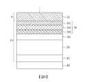
在圖7中,第二磊晶區(未示出)中的各磊晶層是N型材料。In FIG. 7, each epitaxial layer in the second epitaxial region (not shown) is an N-type material.
參圖6,首先,基板10之上是依序磊晶成長N型緩衝層12、N型下DBR層20與N型磊晶層395;接著,在N型磊晶層395之上磊晶成長穿隧接面層393。接著,穿隧接面層393之上依序形成P型磊晶層391、P型氧化層361與P型第一下間隔層30。如圖7所示,第二下間隔層30包含由N型磊晶層395、穿隧接面層393與P型磊晶層391構成的PN轉換結構。Referring to Fig. 6, firstly, on the
在圖7雖然第一磊晶區E1包含較多的磊晶層(P型第一下間隔層30、氧化層361、第二下間隔層39及下DBR層20),由於下DBR層20是N型磊晶層,因此第一磊晶區E1的各磊晶層的材料電阻總合並不會過大,且對光的吸收也較少且導熱性較佳。如此,第一磊晶區E1中可進一步增設有助於提升VCSEL特性的磊晶層, 進一步增進VCSEL的出光功率、光電轉換效率(power conversion efficiency)或特性。In FIG. 7, although the first epitaxial region E1 contains more epitaxial layers (P-type first
在一些實施例中,在第一磊晶區與第二磊晶區中分別設置一或多個的氧化層、間隔層與其他適當磊晶層。氧化層與間隔層的配置數目與配置位置係依照VCSEL所需特性而定。In some embodiments, one or moreindividual oxide layers, spacer layers, and other appropriate epitaxial layers. The number and location of the oxide layer and the spacer layer are determined according to the required characteristics of the VCSEL.
以PN轉換結構設置於第二磊晶區E2的上DBR層40為例;當雷射二極體受到順向偏壓時,雖然上DBR層40中的P型磊晶層的電洞遷移率較低,但N型磊晶層的電子遷移率較快,如此第二磊晶區E2的電流散佈會變得較為均勻,因此VCSEL產生的雷射光的發散角較小或VCSEL的出光光形(beam profile)能符合預定的特定光形(例如光形中央的出光強度相對周圍的出光強度比較相近)。Taking the
當P型磊晶層與N型磊晶層的摻雜濃度相同時,由於上DBR層40中的N型磊晶層的電子遷移率快,所以N型DBR層405材料的電阻較小,因此,這些N型DBR層405的摻雜濃度能適度的降低,如此可在不增加上DBR層40材料的電阻的情況下,更進一步減少上DBR層40對光的吸收以提高VCSEL的出光功率。When the doping concentration of the P-type epitaxial layer is the same as that of the N-type epitaxial layer, since the
當下DBR層、第一上間隔層、第二上間隔層、第一下間隔層或第二下間隔層包含PN轉換結構,VCSEL的出光功率與光電轉換效率也能獲得增進。The current DBR layer, the first upper spacer layer, the second upper spacer layer, the first lower spacer layer or the secondThe second lower spacer layer contains a PN conversion structure, and the output power and photoelectric conversion efficiency of the VCSEL can also be improved.
在一些實施例,當歐姆接觸層是包N型GaAs、N型InGaAs、N型GaAsSb、N型InAlGaAs、N型InGaAsSb或以上材料的任意組合。如此,歐姆接觸層材料的電阻能被降低,電流在第二磊晶區中的散佈較為均勻,或VCSEL的電阻能進一步降低。In some embodiments, when the ohmic contact layer is N-type GaAs, N-type InGaAs, N-typeGaAsSb, N-type InAlGaAs, N-type InGaAsSb or any combination of the above materials. In this way, the resistance of the material of the ohmic contact layer can be reduced, and the current spread in the second epitaxial region can be more uniform, or the resistance of the VCSEL can be further reduced.
在一些實施例,歐姆接觸層的摻雜元素是選自於Si、Te及Se的至少其中之一。如此,歐姆接觸層材料的電阻能被降低,電流在第二磊晶區中的散佈較為均勻,或VCSEL的電阻能進一步降低。In some embodiments, the doping element of the ohmic contact layer is selected from Si, Te and Se toOne of them is missing. In this way, the resistance of the material of the ohmic contact layer can be reduced, and the current spread in the second epitaxial region can be more uniform, or the resistance of the VCSEL can be further reduced.
[實施例3][Example 3]
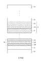
如圖8所示,主動區31包含兩主動層32、321及介於兩主動層32、321之間的穿隧接面層323。As shown in FIG. 8, the active region 31 includes two
在一些實施例中,兩主動層32、321之間也可設置PN轉換結構(後稱另一PN轉換結構),也就是圖8中的穿隧接面層之上與之下更設置N型磊晶層(圖8未示出)與P型磊晶層(圖8未示出)。要注意的是,當另一PN轉換結構設置於主動區中,P型磊晶層的設置位置不受限制,亦即P型磊晶層可設置於穿隧接面層323之上或之下。主動層的層數可以是一層或三層以上。In some embodiments, a PN switching structure can also be set between the two
在一些實施例中,兩主動層之間更設置氧化層及/或間隔層。In some embodiments, an oxide layer and/or a spacer layer are further disposed between the two active layers.
在一實施例中,主動區中的任兩相鄰的主動層之間皆設置穿隧接面層,比如,若主動區包含三層主動層,則最上層的主動層跟在中間的主動層之間設置穿隧接面層,以及在中間的主動層跟最下層的主動層之間也設置穿隧接面層。In one embodiment, a tunnel connection is set between any two adjacent active layers in the active region.surface layer, for example, if the active area includes three active layers, then a tunnel interface layer is set between the uppermost active layer and the middle active layer, and a tunnel interface layer is also set between the middle active layer and the lowermost active layer. Set the tunnel junction layer.
一實施例中,主動區中的任兩相鄰的主動層之間皆設置穿隧接面層與氧化層,比如,若主動區包含三層主動層,則最上層的主動層跟在中間的主動層之間設置穿隧接面層與氧化層,在中間的主動層跟最下層的主動層之間也設置穿隧接面層與氧化層。In one embodiment, a tunnel junction is provided between any two adjacent active layers in the active regionlayer and oxide layer, for example, if the active region contains three active layers, then a tunnel junction layer and an oxide layer are set between the uppermost active layer and the middle active layer, and the middle active layer and the lowermost active layer A tunnel junction layer and an oxide layer are also arranged between the layers.
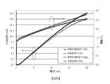
參閱圖9、10,圖9與圖10是圖7的VCSEL與先前技術的VCSEL在室溫下與在高溫下的L-I-V特性圖。上述的室溫與高溫分別為25℃與85℃。Referring to Fig. 9, 10, Fig. 9 and Fig. 10 are the VCSEL of Fig. 7 and the VCSEL of prior artL-I-V characteristic graph at room temperature and at high temperature. The above-mentioned room temperature and high temperature are 25° C. and 85° C., respectively.
本實施例的VCSEL,如圖7所示(參實施例2-3),在第一磊晶區E1的第二下間隔層39包含PN接面,而第二磊晶區則為N型。先前技術的VCSEL與圖7的VCSEL除了上DBR層的總反射率彼此接近外,下DBR層的總反射率亦彼此接近;此外,兩者的氧化層並具有直徑大致相同的電流侷限通孔(optical aperture)。先前技術的VCSEL的結構跟圖7的VCSEL的主要差異在於,先前技術的VCSEL的第二磊晶區的各磊晶層皆為P型;圖7的VCSEL的第一磊晶區中的一些磊晶層是P型,而其他磊晶層(包含下DBR層)則為N型。The VCSEL of this embodiment, as shown in Figure 7 (refer to Embodiment 2-3), in the first epitaxial region E1The second
根據圖9與圖10的出光功率-電流-電壓特性曲線(L-I-V curve)可以發現,圖7的VCSEL的電壓(Vf)在各電流值下皆小於現有技術的VCSEL的電壓(Vf),而圖7的VCSEL的出光功率在定電流值下大於現有技術的VCSEL的出光功率。由此可知,具有PN 接面的VCSEL因具有較多的N型磊晶層,因此VCSEL的電阻較小且出光功率較大。According to the light output power-current-voltage characteristic curve (L-I-V curve) of Figure 9 and Figure 10, it can be found thatNow, the voltage (Vf) of the VCSEL of FIG. 7 is lower than the voltage (Vf) of the VCSEL of the prior art at each current value, and the output power of the VCSEL of FIG. 7 is greater than that of the VCSEL of the prior art at a constant current value. It can be known that the VCSEL with the PN junction has more N-type epitaxial layers, so the resistance of the VCSEL is smaller and the output power of the VCSEL is larger.
當溫度是25℃時,圖7的VCSEL與現有技術的VCSEL在12mA的出光功率分別是11.7mW與11mW。而當溫度從25℃升高到85℃時,圖7的VCSEL的出光功率是從11.7mW稍微下降至9.34mW(在12mA時的出光功率) ,而現有技術的VCSEL的出光功率是從11mW下降至8.4mW。由此可知,具有PN 接面的VCSEL因具有較多的N型磊晶層,因此VCSEL的散熱明顯較佳,亦即,具有PN 接面的VCSEL具有較佳的高溫特性。When the temperature is 25°C, the VCSEL of Figure 7 and the VCSEL of the prior art have an output of 12mAThe optical power is 11.7mW and 11mW respectively. And when the temperature increases from 25°C to 85°C, the light output power of the VCSEL in Figure 7 drops slightly from 11.7mW to 9.34mW (light output power at 12mA), while the light output power of the prior art VCSEL drops from 11mW to 8.4mW. It can be seen that the VCSEL with the PN junction has more N-type epitaxial layers, so the heat dissipation of the VCSEL is obviously better, that is, the VCSEL with the PN junction has better high temperature characteristics.
以上所述者僅為用以解釋本發明之較佳實施例,並非企圖據以對本發明做任何形式上之限制,是以,凡有在相同之發明精神下所作有關本發明之任何修飾或變更,皆仍應包括在本發明意圖保護之範疇。The above descriptions are only used to explain the preferred embodiments of the present invention, and are not intended toThe present invention is limited in any form, so that any modification or change related to the present invention made under the same spirit of the invention should still be included in the intended protection scope of the present invention.
20’:下DBR層30’:下間隔層32’:主動層34’:上間隔層40’:上DBR層100:高功率VCSEL10:GaAs基板12:緩衝層20:下DBR層30:第一下間隔層361、362:氧化層39:第二下間隔層A:主動區32、321:主動層34:第一上間隔層38:第二上間隔層40:上DBR層50:歐姆接觸層201、401、301、341、381、391:P型磊晶層203、303、323、343、383、393、403:穿隧接面層205、305、345、385、395、405:N型磊晶層E1:第一磊晶區E2:第二磊晶區20': Lower DBR layer30': lower spacer layer32': active layer34': upper spacer layer40': Upper DBR layer100: High power VCSEL10: GaAs substrate12: buffer layer20: Lower DBR layer30: The first
圖1為習知技術的VCSEL的示意圖。圖2為依據被描述的一實施例的PN轉換結構設置於VCSEL的上DBR層的示意圖。圖3為依據被描述的一實施例的PN轉換結構設置於VCSEL的第一上間隔層的示意圖,第一上間隔層是位於主動層跟氧化層之間。圖4為依據被描述的一實施例的PN轉換結構設置於VCSEL的第二上間隔層的示意圖,PN轉換結構是位於上DBR層跟氧化層之間。圖5為依據被描述的一實施例的PN轉換結構設置於VCSEL的下DBR層的示意圖。圖6為依據被描述的一實施例的PN轉換結構設置於VCSEL的第一下間隔層的一示意圖,第一下間隔層是位於主動層跟氧化層之間。圖7為依據被描述的一實施例的磊晶轉換結構設置於VCSEL的第二下間隔層的示意圖,第二下間隔層是位於下DBR層跟氧化層之間。圖8為依據被描述的一實施例之包含兩主動層的主動區的VCSEL示意圖。圖9係表示以實施例2-3形成VCSEL(圖7)以及先前技術的VCSEL在室溫下的出光功率-電流-電壓(L-I-V)特性圖。圖10係表示以實施例2-3形成VCSEL(圖7)以及先前技術的VCSEL在高溫下的出光功率-電流-電壓(L-I-V)特性圖。FIG. 1 is a schematic diagram of a VCSEL in the prior art.FIG. 2 is a schematic diagram of a PN switching structure disposed on an upper DBR layer of a VCSEL according to an embodiment described.FIG. 3 is a schematic diagram of a PN switching structure disposed on a first upper spacer layer of a VCSEL according to an embodiment described, and the first upper spacer layer is located between an active layer and an oxide layer.4 is a schematic diagram of a PN switching structure disposed on the second upper spacer layer of a VCSEL according to an embodiment described, the PN switching structure is located between the upper DBR layer and the oxide layer.FIG. 5 is a schematic diagram of a PN switching structure disposed in a lower DBR layer of a VCSEL according to an embodiment described.FIG. 6 is a schematic diagram of a PN switching structure disposed on a first lower spacer layer of a VCSEL according to an embodiment described. The first lower spacer layer is located between the active layer and the oxide layer.FIG. 7 is a schematic diagram of an epitaxial conversion structure disposed on a second lower spacer layer of a VCSEL according to an embodiment described, and the second lower spacer layer is located between the lower DBR layer and the oxide layer.FIG. 8 is a schematic diagram of a VCSEL with an active region including two active layers according to one embodiment described.FIG. 9 is a graph showing the light output power-current-voltage (L-I-V) characteristics of the VCSEL formed in Example 2-3 ( FIG. 7 ) and the VCSEL of the prior art at room temperature.FIG. 10 is a graph showing the output power-current-voltage (L-I-V) characteristics of the VCSEL formed by Example 2-3 ( FIG. 7 ) and the VCSEL of the prior art at high temperature.
100:高功率VCSEL100: High power VCSEL
10:GaAs基板10: GaAs substrate
12:緩衝層12: buffer layer
20:下DBR層20: Lower DBR layer
30:第一下間隔層30: The first lower spacer layer
32:主動層32:Active layer
34:第一上間隔層34: The first upper spacer layer
362:氧化層362: oxide layer
40:上DBR層40: Upper DBR layer
50:歐姆接觸層50: ohmic contact layer
401:P型磊晶層401: P-type epitaxial layer
403:穿隧接面層403: Tunnel junction layer
405:N型磊晶層405: N-type epitaxial layer
A:主動區A: Active area
E1:第一磊晶區E1: the first epitaxial region
E2:第二磊晶區E2: the second epitaxial region
Claims (23)
Translated fromChineseApplications Claiming Priority (2)
| Application Number | Priority Date | Filing Date | Title |
|---|---|---|---|
| TW108134357 | 2019-09-24 | ||
| TW108134357 | 2019-09-24 |
Publications (2)
| Publication Number | Publication Date |
|---|---|
| TW202114312A TW202114312A (en) | 2021-04-01 |
| TWI781445Btrue TWI781445B (en) | 2022-10-21 |
Family
ID=74880164
Family Applications (1)
| Application Number | Title | Priority Date | Filing Date |
|---|---|---|---|
| TW109132787ATWI781445B (en) | 2019-09-24 | 2020-09-22 | High-power vcsel |
Country Status (3)
| Country | Link |
|---|---|
| US (1) | US20210091537A1 (en) |
| CN (1) | CN112636171B (en) |
| TW (1) | TWI781445B (en) |
Families Citing this family (4)
| Publication number | Priority date | Publication date | Assignee | Title |
|---|---|---|---|---|
| WO2022239330A1 (en)* | 2021-05-10 | 2022-11-17 | ソニーセミコンダクタソリューションズ株式会社 | Surface-emitting laser, surface-emitting laser array, and electronic apparatus |
| TW202316758A (en)* | 2021-10-14 | 2023-04-16 | 全新光電科技股份有限公司 | Vcsel with small divergence angle |
| US20230307889A1 (en)* | 2022-03-23 | 2023-09-28 | Visual Photonics Epitaxy Co., Ltd. | Vertical cavity surface-emitting laser epitaxial structure having a current spreading layer |
| TWI838206B (en)* | 2023-04-10 | 2024-04-01 | 台灣茂矽電子股份有限公司 | Transient-voltage-suppression diode structure and manufacturing method thereof |
Citations (4)
| Publication number | Priority date | Publication date | Assignee | Title |
|---|---|---|---|---|
| TW200417057A (en)* | 2002-09-30 | 2004-09-01 | Lumileds Lighting Llc | Light emitting devices including tunnel junctions |
| TW200943653A (en)* | 2008-02-12 | 2009-10-16 | Ricoh Co Ltd | Surface emitting laser element, surface emitting laser array, optical scanning device, and image forming apparatus |
| TW201234585A (en)* | 2010-12-21 | 2012-08-16 | Sumitomo Chemical Co | Semiconductor substrate, method for manufacturing semiconductor substrate and vertical resonator surface light-emitting laser |
| TW201840999A (en)* | 2017-01-06 | 2018-11-16 | 美商普林斯頓光電公司 | Vcsel narrow divergence proximity sensor |
Family Cites Families (12)
| Publication number | Priority date | Publication date | Assignee | Title |
|---|---|---|---|---|
| US6760357B1 (en)* | 1998-04-14 | 2004-07-06 | Bandwidth9 | Vertical cavity apparatus with tunnel junction |
| US6810065B1 (en)* | 2000-11-28 | 2004-10-26 | Optical Communication Productions, Inc. | Low electrical resistance n-type mirror for optoelectronic devices |
| US6515308B1 (en)* | 2001-12-21 | 2003-02-04 | Xerox Corporation | Nitride-based VCSEL or light emitting diode with p-n tunnel junction current injection |
| JP2004296972A (en)* | 2003-03-28 | 2004-10-21 | Yokogawa Electric Corp | Surface emitting laser |
| JP2006294811A (en)* | 2005-04-08 | 2006-10-26 | Fuji Xerox Co Ltd | Tunnel-junction surface emitting semiconductor laser element and manufacturing method thereof |
| DE102007011804A1 (en)* | 2007-01-25 | 2008-07-31 | Osram Opto Semiconductors Gmbh | Measuring arrangement and measuring system |
| CN101599518B (en)* | 2008-06-05 | 2012-05-23 | 广镓光电股份有限公司 | Optoelectronic component and method for the production thereof |
| CN101685942A (en)* | 2008-09-27 | 2010-03-31 | 中国科学院上海微系统与信息技术研究所 | Vertical-cavity surface-emitting laser with InAsP/InGaAsP quantum well as an active layer and method |
| JP5434201B2 (en)* | 2009-03-23 | 2014-03-05 | ソニー株式会社 | Semiconductor laser |
| US8654811B2 (en)* | 2010-08-25 | 2014-02-18 | Flir Systems, Inc. | Serially interconnected vertical-cavity surface emitting laser arrays |
| CN104577711A (en)* | 2013-10-24 | 2015-04-29 | 中国科学院苏州纳米技术与纳米仿生研究所 | Vertical-cavity surface-emitting laser and manufacturing method thereof |
| US20160049502A1 (en)* | 2014-08-15 | 2016-02-18 | Visual Photonics Epitaxy Co., Ltd. | Heterojunction bipolar transistor with blocking layer structure |
- 2020
- 2020-09-22TWTW109132787Apatent/TWI781445B/enactive
- 2020-09-23CNCN202011007258.6Apatent/CN112636171B/ennot_activeExpired - Fee Related
- 2020-09-23USUS17/029,177patent/US20210091537A1/ennot_activeAbandoned
Patent Citations (4)
| Publication number | Priority date | Publication date | Assignee | Title |
|---|---|---|---|---|
| TW200417057A (en)* | 2002-09-30 | 2004-09-01 | Lumileds Lighting Llc | Light emitting devices including tunnel junctions |
| TW200943653A (en)* | 2008-02-12 | 2009-10-16 | Ricoh Co Ltd | Surface emitting laser element, surface emitting laser array, optical scanning device, and image forming apparatus |
| TW201234585A (en)* | 2010-12-21 | 2012-08-16 | Sumitomo Chemical Co | Semiconductor substrate, method for manufacturing semiconductor substrate and vertical resonator surface light-emitting laser |
| TW201840999A (en)* | 2017-01-06 | 2018-11-16 | 美商普林斯頓光電公司 | Vcsel narrow divergence proximity sensor |
Also Published As
| Publication number | Publication date |
|---|---|
| US20210091537A1 (en) | 2021-03-25 |
| TW202114312A (en) | 2021-04-01 |
| CN112636171A (en) | 2021-04-09 |
| CN112636171B (en) | 2022-04-12 |
Similar Documents
| Publication | Publication Date | Title |
|---|---|---|
| TWI781445B (en) | High-power vcsel | |
| JP6184586B2 (en) | Light emitting assembly comprising a semiconductor stack having an active zone on a cylindrical structure | |
| TWI738388B (en) | Vcsel with multiple current confinement layers | |
| US20070223546A1 (en) | Red light laser | |
| JP7363897B2 (en) | surface emitting laser | |
| US5455429A (en) | Semiconductor devices incorporating p-type and n-type impurity induced layer disordered material | |
| JP2004336039A (en) | GaAs-based long wavelength laser incorporating tunnel junction structure | |
| US20200305354A1 (en) | Led for plant illumination | |
| CN115036789B (en) | GaAs-based high-speed vertical cavity surface emitting laser based on type-II tunnel junction | |
| JP2018500762A (en) | Optoelectronic parts | |
| CN105932542A (en) | Transistor vertical-cavity surface-emitting laser | |
| US12288965B1 (en) | Vertical cavity surface emitting laser structure and manufacturing method thereof | |
| US7271418B2 (en) | Semiconductor apparatus for white light generation and amplification | |
| TWI601308B (en) | Infrared LED | |
| US5138624A (en) | Multiwavelength LED and laser diode optical source | |
| US20170092828A1 (en) | Semiconductor light-emitting element | |
| US20140145647A1 (en) | Optical Tilted Charge Devices And Techniques | |
| CN117424068A (en) | Semiconductor laser diode | |
| US20220302343A1 (en) | Light emitting element | |
| JP3151096B2 (en) | Semiconductor light emitting device | |
| TWI845222B (en) | Surface-emitting laser epitaxial structure with current uniformity layer | |
| KR102714364B1 (en) | VCSEL and VCSEL Array with a Common Anode Structure and Micro VCSEL Array | |
| TWI233704B (en) | Semiconductor structure with white light generator and amplifier | |
| JP7738853B2 (en) | Vertical bipolar transistor and manufacturing method thereof | |
| TWI437730B (en) | Light emitting diode |
Legal Events
| Date | Code | Title | Description |
|---|---|---|---|
| GD4A | Issue of patent certificate for granted invention patent |