Movatterモバイル変換


[0]ホーム

URL:


TWI780709B - Spliced display apparatus - Google Patents

Spliced display apparatus
Download PDF

Info

Publication number
TWI780709B
TWI780709BTW110117761ATW110117761ATWI780709BTW I780709 BTWI780709 BTW I780709BTW 110117761 ATW110117761 ATW 110117761ATW 110117761 ATW110117761 ATW 110117761ATW I780709 BTWI780709 BTW I780709B
Authority
TW
Taiwan
Prior art keywords
display panel
display
outer pin
pixel
bonding area
Prior art date
Application number
TW110117761A
Other languages
Chinese (zh)
Other versions
TW202247129A (en
Inventor
何恕德
施景耀
Original Assignee
友達光電股份有限公司
Priority date (The priority date is an assumption and is not a legal conclusion. Google has not performed a legal analysis and makes no representation as to the accuracy of the date listed.)
Filing date
Publication date
Application filed by 友達光電股份有限公司filedCritical友達光電股份有限公司
Priority to TW110117761ApriorityCriticalpatent/TWI780709B/en
Application grantedgrantedCritical
Publication of TWI780709BpublicationCriticalpatent/TWI780709B/en
Publication of TW202247129ApublicationCriticalpatent/TW202247129A/en

Links

Images

Landscapes

Abstract

A spliced display apparatus includes a plurality of display panels. The display panel includes a first display panel and a second display panel. Each of the display panels has a first side facing one of the neighboring display panels and a second side crossing the first side. Each of the display panels has an outer lead bonding region and includes a substrate, a pixel array and data lines. Outer lead bonding region is between the pixel array and the second side. The pixel array includes a first pixel column. The first pixel column is adjacent to the first side. The data lines include a first fan out line and a second fan out line. The first fan out line is electrically connected to the first pixel column of the first display panel. The second fan out line is electrically connected to the first pixel column of the second display panel. The second fan out line is across the first side of the second display panel and the first side of the first display panel and extends to the outer lead bonding region of the first display panel.

Description

Translated fromChinese
拼接式顯示裝置tiled display device

本發明是有關於一種拼接式顯示裝置。The invention relates to a spliced display device.

微型發光二極體(micro LED)顯示器具有低耗能及高亮度的優點,是許多面板廠所積極開發的重點項目之一。目前微型發光二極體顯示器單一模組的最大尺寸僅為12至14吋,若要大於55吋以上,甚至100吋以上,需要透過拼接多個微型發光二極體顯示器來達成。然而,難以避免可視的拼接縫,像是亮縫、暗縫,或模組亮態暗態顯示不良(mura),降低了顯示器視覺上的品味。The micro light emitting diode (micro LED) display has the advantages of low power consumption and high brightness, and is one of the key projects that many panel manufacturers are actively developing. At present, the maximum size of a single micro-LED display module is only 12 to 14 inches. If it is larger than 55 inches or even 100 inches, it needs to be achieved by splicing multiple micro-light-emitting diode displays. However, it is difficult to avoid visible stitching seams, such as bright seams, dark seams, or poor display (mura) of modules in bright and dark states, which reduces the visual taste of the display.

本發明提供一種拼接式顯示裝置,其拼接縫不可視。The invention provides a splicing display device, the splicing seam of which is invisible.

本發明提供一種拼接式顯示裝置,包括多個顯示面板。顯示面板各具有至少一第一側面對相鄰之顯示面板其中之一以及與第一側相交的第二側,各顯示面板具有外引腳接合區。各顯示面板包括基板、畫素陣列及多條資料線。畫素陣列位於基板上,外引腳接合區位於畫素陣列及第二側之間。資料線位於基板上,且電性連接畫素陣列,畫素陣列包括第一畫素行,第一畫素行鄰近於第一側,顯示面板包括第一顯示面板及第二顯示面板,資料線包括多條第一扇出線及多條第二扇出線。第一扇出線電性連接第一顯示面板的第一畫素行。第二扇出線電性連接第二顯示面板的第一畫素行,第二扇出線跨越第二顯示面板的第一側至第一顯示面板的第一側並延伸至第一顯示面板的外引腳接合區上。The invention provides a spliced display device, which includes a plurality of display panels. Each of the display panels has at least one first side facing one of the adjacent display panels and a second side intersecting the first side, and each display panel has an outer lead bonding area. Each display panel includes a substrate, a pixel array and a plurality of data lines. The pixel array is located on the substrate, and the outer pin bonding area is located between the pixel array and the second side. The data line is located on the substrate and is electrically connected to the pixel array. The pixel array includes a first pixel row adjacent to the first side. The display panel includes a first display panel and a second display panel. The data line includes multiple A first fan-out line and a plurality of second fan-out lines. The first fan-out line is electrically connected to the first pixel row of the first display panel. The second fan-out line is electrically connected to the first pixel row of the second display panel, the second fan-out line crosses the first side of the second display panel to the first side of the first display panel and extends to the outside of the first display panel on the pin land.

本發明提供一種拼接式顯示裝置,包括多個顯示面板及電路板,顯示面板包括第一顯示面板及第二顯示面板。顯示面板各具有至少一第一側面對相鄰之顯示面板其中之一以及與第一側相交的第二側,各顯示面板具有外引腳接合區,且各顯示面板包括基板、畫素陣列及多條資料線。畫素陣列位於基板上,外引腳接合區位於畫素陣列及第二側之間。資料線位於基板上且電性連接畫素陣列,畫素陣列包括第一畫素行,第一畫素行鄰近於第一側。電路板配置於第一顯示面板的外引腳接合區及第二顯示面板的外引腳接合區上,電路板具有多條導線,導線電性連接第二顯示面板的第一畫素行,導線自第二顯示面板的外引腳接合區跨越第二顯示面板的第一側至第一顯示面板的第一側並延伸至第一顯示面板的外引腳接合區上。The present invention provides a spliced display device, which includes a plurality of display panels and circuit boards, and the display panels include a first display panel and a second display panel. Each display panel has at least one first side facing one of the adjacent display panels and a second side intersecting with the first side, each display panel has an outer pin bonding area, and each display panel includes a substrate, a pixel array and Multiple data lines. The pixel array is located on the substrate, and the outer pin bonding area is located between the pixel array and the second side. The data line is located on the substrate and is electrically connected to the pixel array. The pixel array includes a first pixel row adjacent to the first side. The circuit board is arranged on the outer pin bonding area of the first display panel and the outer pin bonding area of the second display panel. The circuit board has a plurality of wires, and the wires are electrically connected to the first pixel row of the second display panel. The outer pin land of the second display panel spans from the first side of the second display panel to the first side of the first display panel and extends onto the outer pin land of the first display panel.

本發明提供一種拼接式顯示裝置,包括母板及多個顯示面板。母板具有支撐基材及位於支撐基材上之多條導線。顯示面板位於母板上且各具有至少一第一側面對相鄰之顯示面板其中之一以及與第一側相交的第二側,各顯示面板具有外引腳接合區,且各顯示面板包括基板及畫素陣列。基板具有多個導電通孔。畫素陣列位於基板上,外引腳接合區位於畫素陣列及第二側之間,畫素陣列包括第一畫素行,第一畫素行鄰近於第一側,顯示面板包括第一顯示面板及第二顯示面板,導線透過導電通孔電性連接第二顯示面板的第一畫素行,導線自第二顯示面板的外引腳接合區跨越第二顯示面板的第一側至第一顯示面板的第一側並延伸至第一顯示面板的外引腳接合區上。The invention provides a spliced display device, which includes a motherboard and a plurality of display panels. The motherboard has a support substrate and a plurality of wires located on the support substrate. The display panels are located on the motherboard and each has at least one first side facing one of the adjacent display panels and a second side intersecting the first side, each display panel has an outer pin bonding area, and each display panel includes a substrate and pixel arrays. The substrate has a plurality of conductive vias. The pixel array is located on the substrate, the outer pin bonding area is located between the pixel array and the second side, the pixel array includes a first pixel row, and the first pixel row is adjacent to the first side, and the display panel includes the first display panel and The second display panel, the wire is electrically connected to the first pixel row of the second display panel through the conductive via hole, and the wire crosses the first side of the second display panel from the outer pin bonding area of the second display panel to the first display panel of the first display panel. The first side extends to the outer pin bonding area of the first display panel.

基於上述,在本發明一實施例的拼接式顯示裝置中,顯示面板各具有至少一第一側面對相鄰之顯示面板其中之一,第一扇出線電性連接第一顯示面板的第一畫素行。第二扇出線電性連接第二顯示面板的第一畫素行,第二扇出線跨越第二顯示面板的第一側至第一顯示面板的第一側並延伸至第一顯示面板的外引腳接合區上。藉此,第一顯示面板的第一側及第二顯示面板的第一側之拼接縫左右兩側的第一畫素行可由單一外接電路控制。藉由單一外接電路來調整第一畫素行之灰階,可使拼接縫不可視。Based on the above, in a spliced display device according to an embodiment of the present invention, each display panel has at least one first side facing one of the adjacent display panels, and the first fan-out line is electrically connected to the first side of the first display panel. Pixel row. The second fan-out line is electrically connected to the first pixel row of the second display panel, the second fan-out line crosses the first side of the second display panel to the first side of the first display panel and extends to the outside of the first display panel on the pin land. Thereby, the first pixel rows on the left and right sides of the seam between the first side of the first display panel and the first side of the second display panel can be controlled by a single external circuit. Adjusting the gray scale of the first pixel row by a single external circuit can make the stitching seam invisible.

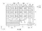
第1圖是依照本發明一實施例的拼接式顯示裝置10的上視示意圖。請參照第1圖,拼接式顯示裝置10包括多個顯示面板100。顯示面板100各具有至少一第一側a1面對相鄰之顯示面板100其中之一以及與第一側a1相交的第二側a2。為了方便說明,第1圖中繪示了第一方向D1及第二方向D2,第一方向D1與第二方向D2相交。舉例而言,第一方向D1與第二方向D2垂直,然而本發明不限於此。於本實施例中,第一側a1平行於第一方向D1,第二側a2平行於第二方向D2。FIG. 1 is a schematic top view of a spliceddisplay device 10 according to an embodiment of the present invention. Please refer to FIG. 1 , the spliceddisplay device 10 includes a plurality ofdisplay panels 100 . Each of thedisplay panels 100 has at least one first side a1 facing one of theadjacent display panels 100 and a second side a2 intersecting the first side a1 . For the convenience of illustration, the first direction D1 and the second direction D2 are shown in the first figure, and the first direction D1 intersects with the second direction D2. For example, the first direction D1 is perpendicular to the second direction D2, but the invention is not limited thereto. In this embodiment, the first side a1 is parallel to the first direction D1, and the second side a2 is parallel to the second direction D2.

各顯示面板100包括基板102、畫素陣列AR及多條資料線DL。畫素陣列AR位於基板102上。資料線DL位於基板102上,且電性連接畫素陣列AR。基板102的材質例如為玻璃、石英、塑膠、有機聚合物、不透光/反射材料(例如:導電材料、金屬、晶圓、陶瓷、或其他可適用的材料)或是其他可適用的材料。在一些實施例中,基板102也可為可撓性基板,其材質包括有機聚合物,例如:聚醯亞胺(polyimide,PI)、聚萘二甲酸乙醇酯(polyethylene naphthalate,PEN)或其它合適的材料,本發明不以此為限。舉例而言,基板102可為黃色聚醯亞胺基板。Eachdisplay panel 100 includes asubstrate 102 , a pixel array AR and a plurality of data lines DL. The pixel array AR is located on thesubstrate 102 . The data line DL is located on thesubstrate 102 and is electrically connected to the pixel array AR. The material of thesubstrate 102 is, for example, glass, quartz, plastic, organic polymer, opaque/reflective material (eg, conductive material, metal, wafer, ceramic, or other applicable materials) or other applicable materials. In some embodiments, thesubstrate 102 can also be a flexible substrate, and its material includes organic polymers, such as polyimide (polyimide, PI), polyethylene naphthalate (polyethylene naphthalate, PEN) or other suitable materials, the present invention is not limited thereto. For example, thesubstrate 102 can be a yellow polyimide substrate.

各顯示面板100具有外引腳接合區103,用以連接外部電路。外部電路例如是驅動晶片、控制電路、軟性印刷電路(flexible printed circuit,FPC)或配置有驅動晶片的印刷電路板(printed circuit board,PCB)等,軟性印刷電路舉例可為液晶高分子軟性印刷電路板(Liquid Crystal Polymer (LCP) FPC board),以使畫素陣列AR能夠被驅動。外引腳接合區103位於畫素陣列AR及第二側a2之間。Eachdisplay panel 100 has an externalpin bonding area 103 for connecting external circuits. The external circuit is, for example, a driver chip, a control circuit, a flexible printed circuit (flexible printed circuit, FPC) or a printed circuit board (printed circuit board, PCB) equipped with a driver chip, etc. The flexible printed circuit can be, for example, a liquid crystal polymer flexible printed circuit Board (Liquid Crystal Polymer (LCP) FPC board), so that the pixel array AR can be driven. The outerpin bonding area 103 is located between the pixel array AR and the second side a2.

舉例而言,顯示面板100包括第一顯示面板100A及第二顯示面板100B,拼接式顯示裝置10還包括驅動元件104,驅動元件104包括第一驅動元件104A及第二驅動元件104B。第一驅動元件104A位於第一顯示面板100的外引腳接合區103上,第二驅動元件104B位於第二顯示面板100B的外引腳接合區103上。第一顯示面板100B的外引腳接合區103連接第一驅動元件104A。第二顯示面板100B的外引腳接合區103連接第二驅動元件104B,第一驅動元件104A和第二驅動元件104B互相電性獨立。For example, thedisplay panel 100 includes afirst display panel 100A and asecond display panel 100B, and themosaic display device 10 further includes adriving element 104 , and thedriving element 104 includes afirst driving element 104A and asecond driving element 104B. Thefirst driving element 104A is located on the outerpin bonding area 103 of thefirst display panel 100 , and thesecond driving element 104B is located on the outerpin bonding area 103 of thesecond display panel 100B. The outerpin bonding area 103 of thefirst display panel 100B is connected to thefirst driving element 104A. The outerpin bonding area 103 of thesecond display panel 100B is connected to thesecond driving element 104B, and thefirst driving element 104A and thesecond driving element 104B are electrically independent from each other.

於本實施例中,畫素陣列AR包括第一畫素行106,第一畫素行106鄰近於第一側a1。資料線DL包括多條第一扇出線108及多條第二扇出線110。第一扇出線108電性連接第一顯示面板100A的第一畫素行106。第二扇出線110電性連接第二顯示面板100B的第一畫素行106,第二扇出線110跨越第二顯示面板100B的第一側a1至第一顯示面板100A的第一側a1並延伸至第一顯示面板100A的外引腳接合區103上。藉此,第一顯示面板100A的第一側a1及第二顯示面板100B的第一側a1之拼接縫112左右兩側的第一畫素行106都是由第一驅動元件104A所控制,換言之,由單一驅動元件控制。藉由單一驅動元件來調整第一畫素行106之灰階(即亮度),可使拼接縫112不可視。In this embodiment, the pixel array AR includes afirst pixel row 106 adjacent to the first side a1. The data lines DL include a plurality of first fan-outlines 108 and a plurality of second fan-outlines 110 . The first fan-outline 108 is electrically connected to thefirst pixel row 106 of thefirst display panel 100A. The second fan-outline 110 is electrically connected to thefirst pixel row 106 of thesecond display panel 100B, and the second fan-outline 110 crosses the first side a1 of thesecond display panel 100B to the first side a1 of thefirst display panel 100A and extending to the outerpin bonding area 103 of thefirst display panel 100A. Thus, thefirst pixel rows 106 on the left and right sides of theseam 112 on the first side a1 of thefirst display panel 100A and the first side a1 of thesecond display panel 100B are all controlled by thefirst driving element 104A, in other words , controlled by a single drive element. Adjusting the grayscale (ie, brightness) of thefirst pixel row 106 by a single driving element can make thesplicing seam 112 invisible.

各顯示面板100可包括多個接墊113,接墊113位於外引腳接合區103,接墊113的第一部分113A可用於將第一扇出線108及第二扇出線110連接第一驅動元件104A。由於接墊113的尺寸遠大於第一扇出線108及第二扇出線110的線寬,舉例而言,接墊113的面積為數百平方微米。因此,第二扇出線110可打線接合於第一驅動元件104A,不需耗費額外的微影製程,從而使得製程簡單化。於其他實施例中,第二扇出線110可利用噴墨塗佈技術(ink jet printing,IJP)來形成。基於導電性的考量,第一扇出線108及第二扇出線110的材質為金屬(例如鉻、金、銀、銅、錫、鉛、鉿、鎢、鉬、釹、鈦、鉭、鋁、鋅、前述金屬之合金或前述金屬之堆疊層)。然而,本發明不限於此。Eachdisplay panel 100 may include a plurality ofpads 113, thepads 113 are located in the outerpin bonding area 103, and thefirst portion 113A of thepads 113 can be used to connect the first fan-outline 108 and the second fan-outline 110 to the first driver.Element 104A. Since the size of thepad 113 is much larger than the line width of the first fan-outline 108 and the second fan-outline 110 , for example, the area of thepad 113 is hundreds of square micrometers. Therefore, the second fan-outline 110 can be wire-bonded to thefirst driving element 104A without consuming an extra lithography process, thereby simplifying the process. In other embodiments, the second fan-outline 110 can be formed by ink jet printing (IJP). Based on the consideration of conductivity, the material of the first fan-outline 108 and the second fan-outline 110 is metal (such as chromium, gold, silver, copper, tin, lead, hafnium, tungsten, molybdenum, neodymium, titanium, tantalum, aluminum , zinc, alloys of the aforementioned metals or stacked layers of the aforementioned metals). However, the present invention is not limited thereto.

各畫素陣列AR還包括多個第二畫素行114,第二畫素行114位於第一畫素行106之一側,且第二畫素行114用以顯示畫面,第一顯示面板100A的第二畫素行114A電性連接第一顯示面板100A的外引腳接合區103,第二顯示面板100B的第二畫素行114B電性連接第二顯示面板100B的外引腳接合區103。也就是說,第一顯示面板100A的第二畫素行114A和第二顯示面板100B的第二畫素行114B分別由第一驅動元件104A及第二驅動元件104B所控制,使各第二畫素行114A、114B可獨立顯示畫面。Each pixel array AR also includes a plurality ofsecond pixel rows 114, thesecond pixel rows 114 are located on one side of thefirst pixel row 106, and thesecond pixel rows 114 are used to display pictures, the second picture of thefirst display panel 100A Thepixel row 114A is electrically connected to the outerpin bonding area 103 of thefirst display panel 100A, and thesecond pixel row 114B of thesecond display panel 100B is electrically connected to the outerpin bonding area 103 of thesecond display panel 100B. That is to say, thesecond pixel row 114A of thefirst display panel 100A and thesecond pixel row 114B of thesecond display panel 100B are respectively controlled by thefirst driving element 104A and thesecond driving element 104B, so that eachsecond pixel row 114A , 114B can display the picture independently.

於本實施例中,拼接式顯示裝置10還包括多個遮光部116及遮光層118。遮光部116分別位於相鄰的第二畫素行114A、114B之間以及第一畫素行106及第二畫素行114之間。舉例而言,第一畫素行106及第二畫素行114A、114B各包括紅色發光元件、綠色發光元件及藍色發光元件。遮光部116即俗稱的黑色矩陣(Black Matrix,BM)。遮光部116及遮光層118的材質例如是黑色樹脂,但本發明不以此為限。In this embodiment, the spliceddisplay device 10 further includes a plurality of light-shieldingportions 116 and a light-shielding layer 118 . Thelight shielding portion 116 is respectively located between the adjacentsecond pixel rows 114A and 114B and between thefirst pixel row 106 and thesecond pixel row 114 . For example, thefirst pixel row 106 and thesecond pixel row 114A, 114B each include red light emitting elements, green light emitting elements and blue light emitting elements. The light-shieldingpart 116 is commonly known as a black matrix (Black Matrix, BM). The material of the light-shieldingportion 116 and the light-shielding layer 118 is, for example, black resin, but the invention is not limited thereto.

遮光層118覆蓋第一顯示面板100A的第一側a1及第二顯示面板100B的第一側a1,且可透過噴墨塗佈技術所形成。遮光層118具有第一遮光層120及第二遮光層122,第一遮光層120的寬度w1小於或等於各遮光部116的寬度w2,用以將第一顯示面板100A的第一畫素行106及第二顯示面板100B的第一畫素行106區隔開。Thelight shielding layer 118 covers the first side a1 of thefirst display panel 100A and the first side a1 of thesecond display panel 100B, and can be formed by inkjet coating technology. The light-shielding layer 118 has a first light-shielding layer 120 and a second light-shielding layer 122. The width w1 of the first light-shielding layer 120 is less than or equal to the width w2 of each light-shieldingportion 116, and is used to divide thefirst pixel row 106 and thefirst pixel row 106 of thefirst display panel 100A. Thefirst pixel rows 106 of thesecond display panel 100B are spaced apart.

於一實施例中,拼接式顯示裝置10還包括母板124,第一顯示面板100A及第二顯示面板100B位於母板124上,且透過黏膠126固定於母板124。第二遮光層122位於母板124上,第二扇出線110位於第二遮光層122上,因此,即使受限於拼接機台目前的精度不足以達造成拼接縫112之寬度為零,拼接縫112造成第一顯示面板100A和第二顯示面板100B之間有高低差,第二遮光層122可以將拼接縫112填平,使第二扇出線110受到支撐,提升其可靠度。黏膠126可為光學膠(optical clear adhesive)。In one embodiment, themosaic display device 10 further includes amotherboard 124 on which thefirst display panel 100A and thesecond display panel 100B are located and fixed to themotherboard 124 through an adhesive 126 . The second light-shielding layer 122 is located on themotherboard 124, and the second fan-outline 110 is located on the second light-shielding layer 122. Therefore, even if the current precision of the splicing machine is not enough to achieve the width of thesplicing seam 112 to be zero, Thesplicing seam 112 causes a height difference between thefirst display panel 100A and thesecond display panel 100B, and the second light-shielding layer 122 can fill thesplicing seam 112 to support the second fan-outline 110 and improve its reliability. . The adhesive 126 can be optical clear adhesive.

第3圖是依照本發明另一實施例的拼接式顯示裝置10a的上視示意圖。第3圖之拼接式顯示裝置10a及第1圖之拼接式顯示裝置10的主要差異在於:第一扇出線108各包括第一分支108Y,各第一分支108Y跨越第一顯示面板100A的第一側a1至第二顯示面板100B的第一側a1並延伸至第二顯示面板100B的外引腳接合區103上。藉此,第一顯示面板100A的第一畫素行106還可以是由第二驅動元件104B所控制。FIG. 3 is a schematic top view of a spliceddisplay device 10a according to another embodiment of the present invention. The main difference between the spliceddisplay device 10a in FIG. 3 and the spliceddisplay device 10 in FIG. 1 is that each of the first fan-outlines 108 includes afirst branch 108Y, and eachfirst branch 108Y straddles the first branch of thefirst display panel 100A. One side a1 extends to the first side a1 of thesecond display panel 100B and extends to the outerpin bonding area 103 of thesecond display panel 100B. Accordingly, thefirst pixel row 106 of thefirst display panel 100A can also be controlled by thesecond driving element 104B.

於一實施例中,第二扇出線110各包括第二分支110Y,各第二分支110Y延伸至第二顯示面板100B的外引腳接合區103上。藉此,第二顯示面板100B的第一畫素行106還可以是由第二驅動元件104B所控制。藉此,第一顯示面板100A的第一側a1及第二顯示面板100B的第一側a1之拼接縫112左右兩側的第一畫素行106還可以都是由第二驅動元件104B所控制,換言之,由單一外接電路控制。藉由單一外接電路來調整第一畫素行106之灰階(即亮度),可使拼接縫112不可視。In one embodiment, each of the second fan-outlines 110 includes asecond branch 110Y, and eachsecond branch 110Y extends to the outerpin bonding area 103 of thesecond display panel 100B. Accordingly, thefirst pixel row 106 of thesecond display panel 100B can also be controlled by thesecond driving element 104B. In this way, thefirst pixel rows 106 on the left and right sides of thesplicing seam 112 on the first side a1 of thefirst display panel 100A and the first side a1 of thesecond display panel 100B can also be controlled by the second driving element 104B. , in other words, controlled by a single external circuit. Adjusting the gray scale (ie brightness) of thefirst pixel row 106 by a single external circuit can make theseam 112 invisible.

第4圖是依照本發明另一實施例的拼接式顯示裝置10b的上視示意圖。第4圖之拼接式顯示裝置10b及第1圖之拼接式顯示裝置10的主要差異在於:第二顯示面板100B的畫素陣列AR還包括第三畫素行128,資料線DL還包括多條第三扇出線130,第三扇出線130電性連接第二顯示面板100B的第三畫素行128,第三扇出線130跨越第二顯示面板100B的第一側a1至第一顯示面板100A的第一側a1並延伸至第一顯示面板100A的外引腳接合區103上。藉此,第二顯示面板100B的第一畫素行106及第三畫素行128都是由第一驅動元件104A所控制。換言之,第二顯示面板100B的最左兩排畫素行可由單一外接電路控制。藉由單一外接電路來調整第一畫素行106及第三畫素行128之灰階(即亮度),可使拼接縫112不可視。且藉由這樣的配置,可依照產品需求調整多個畫素行的灰階。FIG. 4 is a schematic top view of a spliceddisplay device 10b according to another embodiment of the present invention. The main difference between the spliceddisplay device 10b in FIG. 4 and the spliceddisplay device 10 in FIG. 1 is that the pixel array AR of thesecond display panel 100B also includes athird pixel row 128, and the data line DL also includes a plurality of first pixel rows. Three fan-outlines 130, the third fan-outline 130 is electrically connected to thethird pixel row 128 of thesecond display panel 100B, the third fan-outline 130 spans the first side a1 of thesecond display panel 100B to thefirst display panel 100A The first side a1 of thefirst display panel 100A extends to the outerpin bonding area 103 of thefirst display panel 100A. Thus, thefirst pixel row 106 and thethird pixel row 128 of thesecond display panel 100B are controlled by thefirst driving element 104A. In other words, the leftmost two pixel rows of thesecond display panel 100B can be controlled by a single external circuit. Adjusting the gray scale (ie brightness) of thefirst pixel row 106 and thethird pixel row 128 by a single external circuit can make thesplicing seam 112 invisible. And with such a configuration, the gray levels of multiple pixel rows can be adjusted according to product requirements.

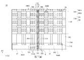
第5圖是依照本發明另一實施例的拼接式顯示裝置20的上視示意圖。第6圖是沿著第5圖的剖線6-6’的剖面示意圖,第5圖及第6圖的實施例沿用第1圖至第2圖的實施例的元件標號與部分內容,其中採用相同或近似的標號來表示相同或近似的元件,並且省略了相同技術內容的說明。關於省略部分的說明可參考前述實施例,在此不贅述。FIG. 5 is a schematic top view of a spliceddisplay device 20 according to another embodiment of the present invention. Fig. 6 is a schematic cross-sectional view along the section line 6-6' of Fig. 5, and the embodiments of Fig. 5 and Fig. 6 follow the component numbers and parts of the embodiments of Fig. 1 to Fig. 2, wherein The same or similar reference numerals denote the same or similar elements, and descriptions of the same technical contents are omitted. For the description of the omitted part, reference may be made to the foregoing embodiments, and details are not repeated here.

拼接式顯示裝置20包括多個顯示面板200。顯示面板200各具有至少一第一側a1面對相鄰之顯示面板200其中之一以及與第一側a1相交的第二側a2,各顯示面板200具有外引腳接合區203,且各顯示面板200包括基板202、畫素陣列AR及多條資料線DL。畫素陣列AR位於基板202上,外引腳接合區203位於畫素陣列AR及第二側a2之間。多條資料線DL位於基板202上,且電性連接畫素陣列AR,畫素陣列AR包括第一畫素行206,第一畫素行206鄰近於第一側a1,顯示面板200包括第一顯示面板200A及第二顯示面板200B。The spliceddisplay device 20 includes a plurality ofdisplay panels 200 . Thedisplay panels 200 each have at least one first side a1 facing one of theadjacent display panels 200 and a second side a2 intersecting the first side a1, eachdisplay panel 200 has an outerpin bonding area 203, and each display Thepanel 200 includes asubstrate 202, a pixel array AR and a plurality of data lines DL. The pixel array AR is located on thesubstrate 202, and the outerpin bonding area 203 is located between the pixel array AR and the second side a2. A plurality of data lines DL are located on thesubstrate 202 and are electrically connected to the pixel array AR. The pixel array AR includes afirst pixel row 206, and thefirst pixel row 206 is adjacent to the first side a1. Thedisplay panel 200 includes afirst display panel 200A and asecond display panel 200B.

電路板208配置於第一顯示面板200A的外引腳接合區203及第二顯示面板200B的外引腳接合區203上,電路板208具有基板SB及位於基板SB上的多個接墊PD,各接墊PD對應於第一顯示面板200A及第二顯示面板200B的接墊213,電路板208具有位於基板SB上的多條導線210,導線210電性連接第二顯示面板200B的第一畫素行206,導線210自第二顯示面板200B的外引腳接合區203跨越第二顯示面板200B的第一側a1至第一顯示面板200A的第一側a1並延伸至第一顯示面板200A的外引腳接合區203上。藉此,第一顯示面板200A的第一側a1及第二顯示面板200B的第一側a1之拼接縫212左右兩側的第一畫素行206都是由第一驅動元件204A所控制,換言之,由單一驅動元件控制。藉由單一驅動元件來調整第一畫素行206之灰階(即亮度),可使拼接縫212不可視。Thecircuit board 208 is disposed on the outerpin bonding area 203 of thefirst display panel 200A and the outerpin bonding area 203 of thesecond display panel 200B, thecircuit board 208 has a substrate SB and a plurality of pads PD located on the substrate SB, Each pad PD corresponds to thepad 213 of thefirst display panel 200A and thesecond display panel 200B. Thecircuit board 208 has a plurality ofwires 210 on the substrate SB. Thewires 210 are electrically connected to the first panel of thesecond display panel 200B.Element row 206,wires 210 cross the first side a1 of thesecond display panel 200B from the outerpin bonding area 203 of thesecond display panel 200B to the first side a1 of thefirst display panel 200A and extend to the outside of thefirst display panel 200A on thepin land 203 . Thus, thefirst pixel rows 206 on the left and right sides of theseam 212 on the first side a1 of thefirst display panel 200A and the first side a1 of thesecond display panel 200B are all controlled by thefirst driving element 204A, in other words , controlled by a single drive element. Adjusting the grayscale (ie, brightness) of thefirst pixel row 206 by a single driving element can make thesplicing seam 212 invisible.

第二遮光層122位於母板224上,因此,即使拼接精度不高,造成拼接縫212之寬度不為零,拼接縫212造成第一顯示面板200A和第二顯示面板200B之間有高低差,第二遮光層122可以將拼接縫212填平,使電路板208受到支撐,提升其可靠度。The second light-shielding layer 122 is located on themotherboard 224. Therefore, even if the splicing accuracy is not high, the width of thesplicing seam 212 is not zero, and thesplicing seam 212 causes a gap between thefirst display panel 200A and thesecond display panel 200B. Poor, the second light-shielding layer 122 can fill up thesplicing seam 212 to support thecircuit board 208 and improve its reliability.

於本實施例中,拼接式顯示裝置20還包括異方性導電膠214,異方性導電膠214位於電路板208及第一顯示面板200A之間,且位於電路板208及第二顯示面板200B之間,用於將電路板208固定於第一顯示面板200A及第二顯示面板200B。In this embodiment, the spliceddisplay device 20 further includes an anisotropicconductive adhesive 214, and the anisotropicconductive adhesive 214 is located between thecircuit board 208 and thefirst display panel 200A, and is located between thecircuit board 208 and thesecond display panel 200B. Between, for fixing thecircuit board 208 on thefirst display panel 200A and thesecond display panel 200B.

第7圖是依照本發明一實施例的拼接式顯示裝置30的俯視示意圖,第8圖是第7圖的區域R的放大示意圖。第9圖是沿著8圖的剖線9a-9a’及9b-9b’的剖面示意圖。第7圖至第9圖的實施例沿用第1圖至第2圖的實施例的元件標號與部分內容,其中採用相同或近似的標號來表示相同或近似的元件,並且省略了相同技術內容的說明。關於省略部分的說明可參考前述實施例,在此不贅述。FIG. 7 is a schematic top view of atiled display device 30 according to an embodiment of the present invention, and FIG. 8 is an enlarged schematic view of a region R in FIG. 7 . Fig. 9 is a schematic cross-sectional view along thesection lines 9a-9a' and 9b-9b' in Fig. 8 . The embodiments in Fig. 7 to Fig. 9 continue to use the component numbers and partial contents of the embodiments in Fig. 1 to Fig. 2, wherein the same or similar symbols are used to represent the same or similar components, and the same technical contents are omitted. illustrate. For the description of the omitted part, reference may be made to the foregoing embodiments, and details are not repeated here.

拼接式顯示裝置30包括母板324及多個顯示面板300。母板324具有支撐基材326及位於支撐基材326上之多條導線328。於一實施例中,母板324還包括多個接墊305,接墊305位於導線328上。The spliceddisplay device 30 includes amotherboard 324 and a plurality ofdisplay panels 300 . Themotherboard 324 has a supportingsubstrate 326 and a plurality ofwires 328 on the supportingsubstrate 326 . In one embodiment, themotherboard 324 further includes a plurality ofpads 305 located on thewires 328 .

基於導電性的考量,導線328的材質為金屬(例如鉻、金、銀、銅、錫、鉛、鉿、鎢、鉬、釹、鈦、鉭、鋁、鋅、前述金屬之合金或前述金屬之堆疊層)。然而,本發明不限於此。Based on the consideration of conductivity, the material of thewire 328 is metal (such as chromium, gold, silver, copper, tin, lead, hafnium, tungsten, molybdenum, neodymium, titanium, tantalum, aluminum, zinc, alloys of the aforementioned metals, or combinations of the aforementioned metals. stacked layers). However, the present invention is not limited thereto.

顯示面板300位於母板324上且各具有至少一第一側a1面對相鄰之顯示面板300其中之一以及與第一側a1相交的第二側a2,各顯示面板300具有外引腳接合區303,且各顯示面板300包括基板302及畫素陣列AR。基板302具有多個導電通孔V。Thedisplay panels 300 are located on themotherboard 324 and each has at least one first side a1 facing one of theadjacent display panels 300 and a second side a2 intersecting the first side a1, and eachdisplay panel 300 has an external pinjoint region 303 , and eachdisplay panel 300 includes asubstrate 302 and a pixel array AR. Thesubstrate 302 has a plurality of conductive vias V. As shown in FIG.

畫素陣列AR位於基板302上,外引腳接合區303位於畫素陣列AR及第二側a2之間,畫素陣列AR包括第一畫素行306,第一畫素行306鄰近於第一側a1,顯示面板300包括第一顯示面板300A及第二顯示面板300B。The pixel array AR is located on thesubstrate 302, the outerpin bonding area 303 is located between the pixel array AR and the second side a2, the pixel array AR includes afirst pixel row 306, and thefirst pixel row 306 is adjacent to the first side a1 , thedisplay panel 300 includes afirst display panel 300A and asecond display panel 300B.

各顯示面板300可包括多個接墊314,接墊314位於外引腳接合區303,資料線DL還包括多條第一扇出線308及多條第二扇出線310,接墊314包含第一部分314A用於將第二扇出線310連接第一驅動元件304A。接墊314的第一部分314A重疊於母板324的接墊305,且接墊314的第一部分314A透過導電通孔V電性連接母板324的接墊305。Eachdisplay panel 300 may include a plurality ofpads 314, and thepads 314 are located in the outerpin bonding area 303. The data line DL also includes a plurality of first fan-outlines 308 and a plurality of second fan-outlines 310. Thepads 314 include Thefirst part 314A is used to connect the second fan-outline 310 to thefirst driving element 304A. Thefirst portion 314A of thepad 314 overlaps thepad 305 of themotherboard 324 , and thefirst portion 314A of thepad 314 is electrically connected to thepad 305 of themotherboard 324 through the conductive via V.

導線328自第二顯示面板300B的外引腳接合區303跨越第二顯示面板300A的第一側a1至第一顯示面板300B的第一側a1並延伸至第一顯示面板300A的外引腳接合區303上,導線328透過導電通孔V電性連接第二顯示面板300B的第一畫素行306。Thewire 328 crosses the first side a1 of thesecond display panel 300A from the outerpin bonding area 303 of thesecond display panel 300B to the first side a1 of thefirst display panel 300B and extends to the outer pin bonding area of thefirst display panel 300A. On theregion 303 , thewire 328 is electrically connected to thefirst pixel row 306 of thesecond display panel 300B through the conductive via V.

舉例而言,第一驅動元件304A的訊號沿著箭頭316自第一顯示面板300A的接墊314的第一部分314A傳遞至導電通孔V及母板324的接墊305,然後經過母板324的導線328,再傳遞至母板324的接墊305及導電通孔V,最後傳遞至第二顯示面板300B的接墊314的第一部分314A,使第二顯示面板300B的第一畫素行306接收到訊號。For example, the signal of thefirst driving element 304A is transmitted from thefirst portion 314A of thepad 314 of thefirst display panel 300A to the conductive via V and thepad 305 of themotherboard 324 along thearrow 316, and then passes through thepad 305 of themotherboard 324. Thewire 328 is then transmitted to thepad 305 and the conductive via V of themotherboard 324, and finally transmitted to thefirst part 314A of thepad 314 of thesecond display panel 300B, so that thefirst pixel row 306 of thesecond display panel 300B receives signal.

藉此,第一顯示面板300A的第一側a1及第二顯示面板300B的第一側a1之拼接縫312左右兩側的第一畫素行306都是由第一驅動元件304A所控制,換言之,由單一驅動元件控制。藉由單一驅動元件來調整第一畫素行306之灰階(即亮度),可使拼接縫312不可視。Thus, thefirst pixel rows 306 on the left and right sides of theseam 312 on the first side a1 of thefirst display panel 300A and the first side a1 of thesecond display panel 300B are all controlled by thefirst driving element 304A, in other words , controlled by a single drive element. Adjusting the gray scale (ie, brightness) of thefirst pixel row 306 by a single driving element can make thesplicing seam 312 invisible.

綜上所述,在本發明一實施例的拼接式顯示裝置中,第二扇出線電性連接第二顯示面板的第一畫素行,第二扇出線跨越第二顯示面板的第一側至第一顯示面板的第一側並延伸至第一顯示面板的外引腳接合區上。藉此,第一顯示面板的第一側及第二顯示面板的第一側之拼接縫左右兩側的第一畫素行可由單一外接電路控制。藉由單一外接電路來調整第一畫素行之灰階,可使拼接縫不可視。To sum up, in the spliced display device according to an embodiment of the present invention, the second fan-out line is electrically connected to the first pixel row of the second display panel, and the second fan-out line crosses the first side of the second display panel to the first side of the first display panel and extend to the outer pin bonding area of the first display panel. Thereby, the first pixel rows on the left and right sides of the seam between the first side of the first display panel and the first side of the second display panel can be controlled by a single external circuit. Adjusting the gray scale of the first pixel row by a single external circuit can make the stitching seam invisible.

2-2’,6-6’:剖線 9a-9a’,9b-9b’:剖線 10,10a,10b:拼接式顯示裝置 20,30:拼接式顯示裝置 100:顯示面板 100A:第一顯示面板 100B:第二顯示面板 102:基板 103:外引腳接合區 104:驅動元件 104A:第一驅動元件 104B:第二驅動元件 106:第一畫素行 108:第一扇出線 108Y:第一分支 110:第二扇出線 110Y:第二分支 112:拼接縫 113:接墊 113A:第一部分 114,114A,114B:第二畫素行 116:遮光部 118:遮光層 120:第一遮光層 122:第二遮光層 124:母板 126:黏膠 128:第三畫素行 130:第三扇出線 200:顯示面板 202:基板 203:外引腳接合區 204A:第一驅動元件 206:第一畫素行 208:電路板 210:導線 212:拼接縫 214:異方性導電膠 300:顯示面板 302:基板 303:外引腳接合區 304A:第一驅動元件 305:接墊 306,306B:第一畫素行 308:第一扇出線 310:第二扇出線 314:接墊 314A:第一部分 316:箭頭 324:母板 326:支撐基材 328:導線 a1:第一側 a2:第二側 AR:畫素陣列 D1:第一方向 D2:第二方向 DL:資料線 PD:接墊 SB:基板 V:導電通孔 w1,w2:寬度2-2', 6-6': split line 9a-9a', 9b-9b': broken line 10, 10a, 10b: Mosaic display device 20,30: Mosaic display device 100: display panel 100A: The first display panel 100B: second display panel 102: Substrate 103: Outer pin land 104: drive element 104A: the first driving element 104B: the second driving element 106: The first pixel line 108: The first fan out 108Y: the first branch 110: Second fan outlet 110Y: the second branch 112: stitching seam 113: Pad 113A: Part I 114, 114A, 114B: the second pixel row 116: shading part 118: shading layer 120: the first shading layer 122: the second shading layer 124: motherboard 126: viscose 128: The third pixel line 130: The third fan out 200: display panel 202: Substrate 203: Outer pin land 204A: first driving element 206: The first pixel line 208: circuit board 210: wire 212: stitching seam 214: Anisotropic conductive adhesive 300: display panel 302: Substrate 303: Outer pin land 304A: first driving element 305: Pad 306,306B: the first pixel row 308: The first fan out 310: The second fan out 314: Pad 314A: Part I 316: arrow 324: motherboard 326: supporting substrate 328: wire a1: first side a2: second side AR: pixel array D1: the first direction D2: Second direction DL: data line PD: Pad SB: Substrate V: Conductive Via w1, w2: width

閱讀以下詳細敘述並搭配對應之圖式,可了解本揭露之多個樣態。需留意的是,圖式中的多個特徵並未依照該業界領域之標準作法繪製實際比例。事實上,所述之特徵的尺寸可以任意的增加或減少以利於討論的清晰性。 第1圖是依照本發明一實施例的拼接式顯示裝置的上視示意圖。 第2圖是沿著第1圖的剖線2-2’的剖面示意圖。 第3圖是依照本發明另一實施例的拼接式顯示裝置的上視示意圖。 第4圖是依照本發明另一實施例的拼接式顯示裝置的上視示意圖。 第5圖是依照本發明另一實施例的拼接式顯示裝置的上視示意圖。 第6圖是沿著第5圖的剖線6-6’的剖面示意圖。 第7圖是依照本發明另一實施例的拼接式顯示裝置的上視示意圖。 第8圖是第7圖的區域R的放大示意圖。 第9圖是沿著第8圖的剖線9a-9a’及剖線9b-9b’的剖面示意圖。Read the following detailed description and match the corresponding diagrams to understand the multiple aspects of this disclosure. It should be noted that many features in the drawings are not drawn to scale in accordance with standard practice in this industry. In fact, the dimensions of the described features may be arbitrarily increased or decreased for clarity of discussion. FIG. 1 is a schematic top view of a spliced display device according to an embodiment of the present invention. Fig. 2 is a schematic cross-sectional view along line 2-2' of Fig. 1 . FIG. 3 is a schematic top view of a spliced display device according to another embodiment of the present invention. FIG. 4 is a schematic top view of a spliced display device according to another embodiment of the present invention. FIG. 5 is a schematic top view of a spliced display device according to another embodiment of the present invention. Fig. 6 is a schematic cross-sectional view along line 6-6' of Fig. 5 . FIG. 7 is a schematic top view of a spliced display device according to another embodiment of the present invention. Fig. 8 is an enlarged schematic view of the region R in Fig. 7 . Fig. 9 is a schematic cross-sectional view along thesection line 9a-9a' andsection line 9b-9b' in Fig. 8.

國內寄存資訊(請依寄存機構、日期、號碼順序註記) 無 國外寄存資訊(請依寄存國家、機構、日期、號碼順序註記) 無Domestic deposit information (please note in order of depositor, date, and number) none Overseas storage information (please note in order of storage country, institution, date, and number) none

2-2’:剖線2-2': section line

10:拼接式顯示裝置10: Mosaic display device

100:顯示面板100: display panel

100A:第一顯示面板100A: The first display panel

100B:第二顯示面板100B: second display panel

102:基板102: Substrate

103:外引腳接合區103: Outer pin land

104:驅動元件104: drive element

104A:第一驅動元件104A: the first driving element

104B:第二驅動元件104B: the second driving element

106:第一畫素行106: The first pixel line

108:第一扇出線108: The first fan out

110:第二扇出線110: Second fan outlet

112:拼接縫112: stitching seam

113:接墊113: Pad

113A:第一部分113A: Part I

114,114A,114B:第二畫素行114, 114A, 114B: the second pixel row

116:遮光部116: shading part

118:遮光層118: shading layer

120:第一遮光層120: the first shading layer

122:第二遮光層122: the second shading layer

124:母板124: motherboard

a1:第一側a1: first side

a2:第二側a2: second side

AR:畫素陣列AR: pixel array

D1:第一方向D1: the first direction

D2:第二方向D2: Second direction

DL:資料線DL: data line

w1,w2:寬度w1, w2: width

Claims (10)

Translated fromChinese
一種拼接式顯示裝置,包括:多個顯示面板,該些顯示面板包括一第一顯示面板及一第二顯示面板,各具有至少一第一側面對相鄰之該些顯示面板其中之一以及與該第一側相交的一第二側,其中各該顯示面板具有一外引腳接合區,且各該顯示面板包括:一基板;畫素陣列,位於該基板上,其中該外引腳接合區位於該畫素陣列及該第二側之間;及多條資料線,位於該基板上,且電性連接該畫素陣列,其中該畫素陣列包括一第一畫素行,該第一畫素行鄰近於該第一側,其中該些資料線包括:多條第一扇出線,電性連接該第一顯示面板的該第一畫素行;及多條第二扇出線,電性連接該第二顯示面板的該第一畫素行,其中該些第二扇出線跨越該第二顯示面板的該第一側至該第一顯示面板的該第一側並延伸至該第一顯示面板的該外引腳接合區上。A spliced display device, comprising: a plurality of display panels, the display panels include a first display panel and a second display panel, each having at least one first side facing one of the adjacent display panels and A second side intersected by the first side, wherein each of the display panels has an outer pin bonding area, and each of the display panels includes: a substrate; a pixel array located on the substrate, wherein the outer pin bonding area Located between the pixel array and the second side; and a plurality of data lines located on the substrate and electrically connected to the pixel array, wherein the pixel array includes a first pixel row, the first pixel row Adjacent to the first side, wherein the data lines include: a plurality of first fan-out lines electrically connected to the first pixel row of the first display panel; and a plurality of second fan-out lines electrically connected to the The first pixel row of the second display panel, wherein the second fan-out lines span the first side of the second display panel to the first side of the first display panel and extend to the first display panel on the outer pin land.如請求項1所述之拼接式顯示裝置,其中該些第一扇出線各包括一第一分支,各該第一分支跨越該第一顯示面板的該第一側至該第二顯示面板的該第一側並延伸至該第二顯示面板的該外引腳接合區上。The spliced display device according to claim 1, wherein each of the first fan-out lines includes a first branch, and each of the first branches spans from the first side of the first display panel to the side of the second display panel The first side extends to the outer pin bonding area of the second display panel.如請求項1所述之拼接式顯示裝置,其中該些第二扇出線各包括一第二分支,各該第二分支延伸至該第二顯示面板的該外引腳接合區上。The spliced display device as claimed in claim 1, wherein each of the second fan-out lines includes a second branch, and each of the second branches extends to the outer pin bonding area of the second display panel.如請求項1所述之拼接式顯示裝置,其中各該畫素陣列還包括多個第二畫素行,該些第二畫素行位於該第一畫素行之一側,該第一顯示面板的該些第二畫素行電性連接該第一顯示面板的該外引腳接合區,該第二顯示面板的該些第二畫素行電性連接該第二顯示面板的該外引腳接合區。The spliced display device as described in claim 1, wherein each of the pixel arrays further includes a plurality of second pixel rows, and the second pixel rows are located on one side of the first pixel row, and the first display panel The second pixel rows are electrically connected to the outer pin bonding area of the first display panel, and the second pixel rows of the second display panel are electrically connected to the outer pin bonding area of the second display panel.如請求項1所述之拼接式顯示裝置,其中該第二顯示面板的該畫素陣列還包括一第三畫素行,該些資料線還包括多條第三扇出線,該些第三扇出線電性連接該第二顯示面板的該第三畫素行,該些第三扇出線跨越該第二顯示面板的該第一側至該第一顯示面板的該第一側並延伸至該第一顯示面板的該外引腳接合區上。The spliced display device as described in claim 1, wherein the pixel array of the second display panel further includes a third pixel row, and the data lines also include a plurality of third fan-out lines, and the third fan-out lines The outgoing lines are electrically connected to the third pixel row of the second display panel, and the third fan-out lines cross the first side of the second display panel to the first side of the first display panel and extend to the on the outer pin bonding area of the first display panel.如請求項4所述之拼接式顯示裝置,還包括:多個遮光部,分別位於相鄰的該些第二畫素行之間。The spliced display device according to claim 4 further includes: a plurality of light-shielding parts respectively located between the adjacent second pixel rows.如請求項6所述之拼接式顯示裝置,還包括:一遮光層,覆蓋該第一顯示面板的該第一側及該第二顯示面板的該第一側,該遮光層的寬度小於或等於各該遮光部的寬度。The mosaic display device according to claim 6, further comprising: a light-shielding layer covering the first side of the first display panel and the first side of the second display panel, and the width of the light-shielding layer is less than or equal to shadesection width.如請求項1所述之拼接式顯示裝置,還包括:一驅動元件,位於該第一顯示面板的該外引腳接合區上,其中該些第二扇出線打線接合於該驅動元件。The spliced display device as claimed in claim 1 further includes: a driving element located on the outer pin bonding area of the first display panel, wherein the second fan-out lines are wire-bonded to the driving element.一種拼接式顯示裝置,包括:多個顯示面板,該些顯示面板包括一第一顯示面板及一第二顯示面板,各具有至少一第一側面對相鄰之該些顯示面板其中之一以及與該第一側相交的一第二側,其中各該顯示面板具有一外引腳接合區,且各該顯示面板包括:一基板;一畫素陣列,位於該基板上,其中該外引腳接合區位於該畫素陣列及該第二側之間;及多條資料線,位於該基板上,且電性連接該畫素陣列,其中該畫素陣列包括一第一畫素行,該第一畫素行鄰近於該第一側;及一電路板,配置於該第一顯示面板的該外引腳接合區及該第二顯示面板的該外引腳接合區上,其中該電路板具有多條導線,該些導線電性連接該第二顯示面板的該第一畫素行,該些導線自該第二顯示面板的該外引腳接合區跨越該第二顯示面板的該第一側至該第一顯示面板的該第一側並延伸至該第一顯示面板的該外引腳接合區上。A spliced display device, comprising: a plurality of display panels, the display panels include a first display panel and a second display panel, each having at least one first side facing one of the adjacent display panels and A second side intersected by the first side, wherein each of the display panels has an outer pin bonding area, and each of the display panels includes: a substrate; a pixel array on the substrate, wherein the outer pins are bonded A region is located between the pixel array and the second side; and a plurality of data lines are located on the substrate and electrically connected to the pixel array, wherein the pixel array includes a first pixel row, the first row a row adjacent to the first side; and a circuit board disposed on the outer pin bonding area of the first display panel and the outer pin bonding area of the second display panel, wherein the circuit board has a plurality of wires , the wires are electrically connected to the first pixel row of the second display panel, and the wires cross the first side of the second display panel from the outer pin bonding area of the second display panel to the first The first side of the display panel extends to the outer pin bonding area of the first display panel.一種拼接式顯示裝置,包括:一母板,具有一支撐基材及位於該支撐基材上之多條導線;及多個顯示面板,位於該母板上且各具有至少一第一側面對相鄰之該些顯示面板其中之一以及與該第一側相交的一第二側,其中各該顯示面板具有一外引腳接合區,且各該顯示面板包括:一基板,具有多個導電通孔;及一畫素陣列,位於該基板上,其中該外引腳接合區位於該畫素陣列及該第二側之間,該畫素陣列包括一第一畫素行,該第一畫素行鄰近於該第一側,該些顯示面板包括一第一顯示面板及一第二顯示面板,該些導線透過該些導電通孔電性連接該第二顯示面板的該第一畫素行,該些導線自該第二顯示面板的該外引腳接合區跨越該第二顯示面板的該第一側至該第一顯示面板的該第一側並延伸至該第一顯示面板的該外引腳接合區上。A spliced display device, comprising: a motherboard with a support substrate and a plurality of wires located on the support substrate; and a plurality of display panels located on the motherboard and each having at least one first side facing to each other Adjacent to one of the display panels and a second side intersecting the first side, each of the display panels has an outer pin land, and each of the display panels includes: a substrate having a plurality of conductive vias holes; and a pixel array on the substrate, wherein the outer pin land is located between the pixel array and the second side, the pixel array includes a first pixel row adjacent to the first pixel row On the first side, the display panels include a first display panel and a second display panel, the wires are electrically connected to the first pixel row of the second display panel through the conductive via holes, and the wires are From the outer pin land of the second display panel across the first side of the second display panel to the first side of the first display panel and extending to the outer pin land of the first display panel superior.
TW110117761A2021-05-172021-05-17Spliced display apparatusTWI780709B (en)

Priority Applications (1)

Application NumberPriority DateFiling DateTitle
TW110117761ATWI780709B (en)2021-05-172021-05-17Spliced display apparatus

Applications Claiming Priority (1)

Application NumberPriority DateFiling DateTitle
TW110117761ATWI780709B (en)2021-05-172021-05-17Spliced display apparatus

Publications (2)

Publication NumberPublication Date
TWI780709Btrue TWI780709B (en)2022-10-11
TW202247129A TW202247129A (en)2022-12-01

Family

ID=85462673

Family Applications (1)

Application NumberTitlePriority DateFiling Date
TW110117761ATWI780709B (en)2021-05-172021-05-17Spliced display apparatus

Country Status (1)

CountryLink
TW (1)TWI780709B (en)

Cited By (2)

* Cited by examiner, † Cited by third party
Publication numberPriority datePublication dateAssigneeTitle
TWI873969B (en)*2023-11-102025-02-21友達光電股份有限公司Displaying system
TWI891417B (en)*2024-06-262025-07-21友達光電股份有限公司Splicing display device and driving method thereof

Citations (5)

* Cited by examiner, † Cited by third party
Publication numberPriority datePublication dateAssigneeTitle
US20170132963A1 (en)*2015-06-302017-05-11Boe Technology Group Co., Ltd.Display driving method, display panel and manufacturing method thereof, and display apparatus
US20180108860A1 (en)*2016-10-142018-04-19Boe Technology Group Co., Ltd.Display substrate, display panel and display device
CN108766249A (en)*2018-08-092018-11-06武汉天马微电子有限公司Foldable display panel and foldable display device
CN109935613A (en)*2018-04-182019-06-25友达光电股份有限公司 display panel
US20190266932A1 (en)*2015-06-122019-08-29Boe Technology Group Co., Ltd.Testing method for splicing screens

Patent Citations (5)

* Cited by examiner, † Cited by third party
Publication numberPriority datePublication dateAssigneeTitle
US20190266932A1 (en)*2015-06-122019-08-29Boe Technology Group Co., Ltd.Testing method for splicing screens
US20170132963A1 (en)*2015-06-302017-05-11Boe Technology Group Co., Ltd.Display driving method, display panel and manufacturing method thereof, and display apparatus
US20180108860A1 (en)*2016-10-142018-04-19Boe Technology Group Co., Ltd.Display substrate, display panel and display device
CN109935613A (en)*2018-04-182019-06-25友达光电股份有限公司 display panel
CN108766249A (en)*2018-08-092018-11-06武汉天马微电子有限公司Foldable display panel and foldable display device

Cited By (2)

* Cited by examiner, † Cited by third party
Publication numberPriority datePublication dateAssigneeTitle
TWI873969B (en)*2023-11-102025-02-21友達光電股份有限公司Displaying system
TWI891417B (en)*2024-06-262025-07-21友達光電股份有限公司Splicing display device and driving method thereof

Also Published As

Publication numberPublication date
TW202247129A (en)2022-12-01

Similar Documents

PublicationPublication DateTitle
CN107799008B (en) display device
KR102695728B1 (en)Display device
CN113130463B (en) A light-emitting substrate, its preparation method, and a display device
CN100416353C (en) display device
US12127453B2 (en)Display device having reduced non-display area
US20080024424A1 (en)Liquid Crystal Display Device
CN113075808A (en)Splicing display panel and display device
TWI780709B (en)Spliced display apparatus
KR101348756B1 (en)Film-chip complex and display device having the same
WO2021087726A1 (en)Array substrate, manufacturing method therefor and display device
JP2006209089A (en)Display device
US20240404959A1 (en)Wiring substrate, array substrate and light emitting module having control regions arranged into control region rows and control region columns
TWI734062B (en)Display panel and electronic device
US11410589B2 (en)Display device
TWI791404B (en)Display panel
TWI783875B (en)Display panel
US11798876B2 (en)Chip on film package and display device including the same
KR101033119B1 (en) Line on Glass Liquid Crystal Display
CN220914224U (en)Display device
JP7684851B2 (en) display device
CN119600971A (en) Display device and driving method thereof
CN118645499A (en) Display module and display device
JP2023184061A (en)Display and driver
WO2024060263A1 (en)Display panel, display device and tiled display device
KR20210157945A (en)Display apparatus

Legal Events

DateCodeTitleDescription
GD4AIssue of patent certificate for granted invention patent

[8]ページ先頭

©2009-2025 Movatter.jp