TWI778721B - Flexible sensing device and manufacturing method thereof - Google Patents
Flexible sensing device and manufacturing method thereofDownload PDFInfo
- Publication number
- TWI778721B TWI778721BTW110127155ATW110127155ATWI778721BTW I778721 BTWI778721 BTW I778721BTW 110127155 ATW110127155 ATW 110127155ATW 110127155 ATW110127155 ATW 110127155ATW I778721 BTWI778721 BTW I778721B
- Authority
- TW
- Taiwan
- Prior art keywords
- sensing
- carrier
- dielectric film
- lines
- sensing lines
- Prior art date
Links
Images


Classifications
- G—PHYSICS
- G06—COMPUTING OR CALCULATING; COUNTING
- G06V—IMAGE OR VIDEO RECOGNITION OR UNDERSTANDING
- G06V40/00—Recognition of biometric, human-related or animal-related patterns in image or video data
- G06V40/10—Human or animal bodies, e.g. vehicle occupants or pedestrians; Body parts, e.g. hands
- G06V40/12—Fingerprints or palmprints
- G06V40/13—Sensors therefor
- G06V40/1306—Sensors therefor non-optical, e.g. ultrasonic or capacitive sensing
- H—ELECTRICITY
- H01—ELECTRIC ELEMENTS
- H01L—SEMICONDUCTOR DEVICES NOT COVERED BY CLASS H10
- H01L23/00—Details of semiconductor or other solid state devices
- H01L23/48—Arrangements for conducting electric current to or from the solid state body in operation, e.g. leads, terminal arrangements ; Selection of materials therefor
- H01L23/488—Arrangements for conducting electric current to or from the solid state body in operation, e.g. leads, terminal arrangements ; Selection of materials therefor consisting of soldered or bonded constructions
- H01L23/498—Leads, i.e. metallisations or lead-frames on insulating substrates, e.g. chip carriers
- H01L23/4985—Flexible insulating substrates
- G—PHYSICS
- G06—COMPUTING OR CALCULATING; COUNTING
- G06F—ELECTRIC DIGITAL DATA PROCESSING
- G06F3/00—Input arrangements for transferring data to be processed into a form capable of being handled by the computer; Output arrangements for transferring data from processing unit to output unit, e.g. interface arrangements
- G06F3/01—Input arrangements or combined input and output arrangements for interaction between user and computer
- G06F3/03—Arrangements for converting the position or the displacement of a member into a coded form
- G06F3/041—Digitisers, e.g. for touch screens or touch pads, characterised by the transducing means
- G06F3/0416—Control or interface arrangements specially adapted for digitisers
- G06F3/04164—Connections between sensors and controllers, e.g. routing lines between electrodes and connection pads
- G—PHYSICS
- G06—COMPUTING OR CALCULATING; COUNTING
- G06F—ELECTRIC DIGITAL DATA PROCESSING
- G06F3/00—Input arrangements for transferring data to be processed into a form capable of being handled by the computer; Output arrangements for transferring data from processing unit to output unit, e.g. interface arrangements
- G06F3/01—Input arrangements or combined input and output arrangements for interaction between user and computer
- G06F3/03—Arrangements for converting the position or the displacement of a member into a coded form
- G06F3/041—Digitisers, e.g. for touch screens or touch pads, characterised by the transducing means
- G06F3/044—Digitisers, e.g. for touch screens or touch pads, characterised by the transducing means by capacitive means
- G06F3/0445—Digitisers, e.g. for touch screens or touch pads, characterised by the transducing means by capacitive means using two or more layers of sensing electrodes, e.g. using two layers of electrodes separated by a dielectric layer
- G—PHYSICS
- G06—COMPUTING OR CALCULATING; COUNTING
- G06F—ELECTRIC DIGITAL DATA PROCESSING
- G06F3/00—Input arrangements for transferring data to be processed into a form capable of being handled by the computer; Output arrangements for transferring data from processing unit to output unit, e.g. interface arrangements
- G06F3/01—Input arrangements or combined input and output arrangements for interaction between user and computer
- G06F3/03—Arrangements for converting the position or the displacement of a member into a coded form
- G06F3/041—Digitisers, e.g. for touch screens or touch pads, characterised by the transducing means
- G06F3/044—Digitisers, e.g. for touch screens or touch pads, characterised by the transducing means by capacitive means
- G06F3/0446—Digitisers, e.g. for touch screens or touch pads, characterised by the transducing means by capacitive means using a grid-like structure of electrodes in at least two directions, e.g. using row and column electrodes
- H—ELECTRICITY
- H01—ELECTRIC ELEMENTS
- H01L—SEMICONDUCTOR DEVICES NOT COVERED BY CLASS H10
- H01L21/00—Processes or apparatus adapted for the manufacture or treatment of semiconductor or solid state devices or of parts thereof
- H01L21/02—Manufacture or treatment of semiconductor devices or of parts thereof
- H01L21/04—Manufacture or treatment of semiconductor devices or of parts thereof the devices having potential barriers, e.g. a PN junction, depletion layer or carrier concentration layer
- H01L21/48—Manufacture or treatment of parts, e.g. containers, prior to assembly of the devices, using processes not provided for in a single one of the groups H01L21/18 - H01L21/326 or H10D48/04 - H10D48/07
- H01L21/4814—Conductive parts
- H01L21/4846—Leads on or in insulating or insulated substrates, e.g. metallisation
- H01L21/486—Via connections through the substrate with or without pins
- H—ELECTRICITY
- H01—ELECTRIC ELEMENTS
- H01L—SEMICONDUCTOR DEVICES NOT COVERED BY CLASS H10
- H01L23/00—Details of semiconductor or other solid state devices
- H01L23/48—Arrangements for conducting electric current to or from the solid state body in operation, e.g. leads, terminal arrangements ; Selection of materials therefor
- H01L23/488—Arrangements for conducting electric current to or from the solid state body in operation, e.g. leads, terminal arrangements ; Selection of materials therefor consisting of soldered or bonded constructions
- H01L23/498—Leads, i.e. metallisations or lead-frames on insulating substrates, e.g. chip carriers
- H01L23/49827—Via connections through the substrates, e.g. pins going through the substrate, coaxial cables
- H—ELECTRICITY
- H01—ELECTRIC ELEMENTS
- H01L—SEMICONDUCTOR DEVICES NOT COVERED BY CLASS H10
- H01L23/00—Details of semiconductor or other solid state devices
- H01L23/48—Arrangements for conducting electric current to or from the solid state body in operation, e.g. leads, terminal arrangements ; Selection of materials therefor
- H01L23/488—Arrangements for conducting electric current to or from the solid state body in operation, e.g. leads, terminal arrangements ; Selection of materials therefor consisting of soldered or bonded constructions
- H01L23/498—Leads, i.e. metallisations or lead-frames on insulating substrates, e.g. chip carriers
- H01L23/49866—Leads, i.e. metallisations or lead-frames on insulating substrates, e.g. chip carriers characterised by the materials
- H01L23/49894—Materials of the insulating layers or coatings
- G—PHYSICS
- G06—COMPUTING OR CALCULATING; COUNTING
- G06F—ELECTRIC DIGITAL DATA PROCESSING
- G06F2203/00—Indexing scheme relating to G06F3/00 - G06F3/048
- G06F2203/041—Indexing scheme relating to G06F3/041 - G06F3/045
- G06F2203/04103—Manufacturing, i.e. details related to manufacturing processes specially suited for touch sensitive devices
- G—PHYSICS
- G06—COMPUTING OR CALCULATING; COUNTING
- G06V—IMAGE OR VIDEO RECOGNITION OR UNDERSTANDING
- G06V40/00—Recognition of biometric, human-related or animal-related patterns in image or video data
- G06V40/10—Human or animal bodies, e.g. vehicle occupants or pedestrians; Body parts, e.g. hands
- G06V40/12—Fingerprints or palmprints
- G06V40/13—Sensors therefor
Landscapes
- Engineering & Computer Science (AREA)
- General Physics & Mathematics (AREA)
- Physics & Mathematics (AREA)
- Theoretical Computer Science (AREA)
- General Engineering & Computer Science (AREA)
- Computer Hardware Design (AREA)
- Microelectronics & Electronic Packaging (AREA)
- Power Engineering (AREA)
- Condensed Matter Physics & Semiconductors (AREA)
- Human Computer Interaction (AREA)
- Manufacturing & Machinery (AREA)
- Ceramic Engineering (AREA)
- Multimedia (AREA)
- Computer Networks & Wireless Communication (AREA)
- Measurement Of Length, Angles, Or The Like Using Electric Or Magnetic Means (AREA)
- Measuring Pulse, Heart Rate, Blood Pressure Or Blood Flow (AREA)
- Structure Of Printed Boards (AREA)
Abstract
Translated fromChineseDescription
Translated fromChinese本發明是有關於一種感測裝置,特別是指一種可撓式感測裝置及其製造方法。The present invention relates to a sensing device, in particular to a flexible sensing device and a manufacturing method thereof.
目前用於辨識指紋的感測裝置,包括一矽基板、多條形成於該矽基板的且相間隔交錯的感測線,及一夾置於該等感測線之間的介電膜。A current sensing device for identifying fingerprints includes a silicon substrate, a plurality of sensing lines formed on the silicon substrate and staggered at intervals, and a dielectric film sandwiched between the sensing lines.
然而,受限於矽基板材質與特性,除了必須要搭配半導體廠的專屬設備才能形成該等感測線與該介電膜而不具製程靈活性之外,矽基板本身是一硬質的板狀基材,使得目前感測裝置僅能為硬板態樣。因此,目前感測裝置還有改善空間。However, limited by the material and characteristics of the silicon substrate, the silicon substrate itself is a rigid plate-like substrate, except that the sensing lines and the dielectric film must be formed with the exclusive equipment of the semiconductor factory without process flexibility. , so that the current sensing device can only be in the form of a hard board. Therefore, there is still room for improvement in the current sensing device.
因此,本發明之其中一目的,即在提供一種能夠克服先前技術的至少一個缺點的可撓式感測裝置。Therefore, one of the objectives of the present invention is to provide a flexible sensing device that overcomes at least one disadvantage of the prior art.
於是,本發明可撓式感測裝置,包含一可撓式的載板、多條第一感測線、一介電膜,及多條第二感測線。Therefore, the flexible sensing device of the present invention includes a flexible carrier, a plurality of first sensing lines, a dielectric film, and a plurality of second sensing lines.
該載板選自於一BT(bismaleimide-triazine resin,簡稱BT)載板、一ABF(Ajinomoto Build-up Film)載板,及一聚醯亞胺(polyimide film)載板。The carrier is selected from a BT (bismaleimide-triazine resin, BT for short) carrier, an ABF (Ajinomoto Build-up Film) carrier, and a polyimide film (polyimide film) carrier.
該等第一感測線分別形成於該載板上,並沿一第一方向間隔排列。The first sensing lines are respectively formed on the carrier board and arranged at intervals along a first direction.
該介電膜形成於該等第一感測線上。The dielectric film is formed on the first sensing lines.
該等第二感測線形成於該介電膜上,並沿一相交於該第一方向的第二方向間隔排列。每一第二感測線與該等第一感測線透過該介電膜間隔相交。The second sensing lines are formed on the dielectric film and are arranged at intervals along a second direction intersecting the first direction. Each of the second sensing lines and the first sensing lines intersect with each other through the dielectric film.
因此,本發明之另一目的,即在提供一種能夠克服先前技術的至少一個缺點的可撓式感測裝置的製造方法,包含:一第一感測線形成步驟、一介電膜形成步驟,及一第二感測線形成步驟。Therefore, another object of the present invention is to provide a manufacturing method of a flexible sensing device capable of overcoming at least one disadvantage of the prior art, comprising: a first sensing line forming step, a dielectric film forming step, and a second sensing line forming step.
該第一感測線形成步驟,是在一可撓式的載板上形成多條沿一第一方向間隔排列的第一感測線,該載板選自於一BT載板、一ABF載板,及一聚醯亞胺載板。The step of forming the first sensing line is to form a plurality of first sensing lines spaced along a first direction on a flexible carrier board, the carrier board is selected from a BT carrier board and an ABF carrier board, and a polyimide carrier.
該介電膜形成步驟,是在該等第一感測線上形成一介電膜。The step of forming the dielectric film is to form a dielectric film on the first sensing lines.
該第二感測線形成步驟,是在該介電膜上形成多條沿一相交於該第一方向的第二方向間隔排列的第二感測線,使得每一第二感測線透過該介電膜而與該等第一感測線間隔相交。In the second sensing line forming step, a plurality of second sensing lines are formed on the dielectric film and are spaced along a second direction intersecting the first direction, so that each second sensing line passes through the dielectric film and intersect with the first sensing lines.
本發明之功效在於:透過該載板為可撓式且為特定材質,使該可撓式感測裝置也可撓曲,且製造過程與使用設備也較為彈性。The effect of the present invention is that the flexible sensing device can also be flexed by the carrier board being flexible and made of a specific material, and the manufacturing process and the equipment used are also more flexible.
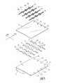
參閱圖1~3,本發明可撓式感測裝置之一第一實施例,包含一載板1,形成於該載板1之多條第一感測線2、一介電膜3及多條第二感測線4、多條第一導接線5、多條第二導接線6,及一設置於該載板1的處理晶片7。Referring to FIGS. 1 to 3 , a first embodiment of the flexible sensing device of the present invention includes a
該載板1為一呈方形的可撓式載板,且具有相反的一第一表面11及一第二表面12,並選自於一BT(bismaleimide-triazine resin,簡稱BT)載板、一ABF(Ajinomoto Build-up Film)載板,及一聚醯亞胺(polyimide film)載板。實施上,該載板1的厚度大於0mm並小於0.5mm,而能在該載板1為可撓式的狀態下,還提供後續形成於其上的膜層一預定的支撐強度。較佳地,該載板1的厚度大於0mm並小於0.1mm。The
該等第一感測線2以薄膜狀的態樣分別形成於該載板1的第一表面11,並沿一第一方向D1間隔排列。該等第一感測線2覆蓋該載板1的第一表面11的部分區域,使得該載板1的第一表面11的其餘部分外露於該等第一感測線2。該等第一感測線2由金屬、合金或導電金屬氧化物製成,且每一第一感測線2沿一垂直於該第一方向D1的第二方向D2延伸,並具有多個沿該第二方向D2間隔排列且為菱形的第一擴大部21,及多條分別連接二相鄰第一擴大部21且寬度小於所述第一擴大部21的第一感測部22。The
該介電膜3形成並覆蓋於該等第一感測線2上,及該第一載板1之未被該等第一感測線2覆蓋的區域。該介電膜3的製成材質選自於聚甲基丙烯酸甲酯(Poly(methyl methacrylate),簡稱PMMA)、聚醯亞胺(polyimide),及已硬化的光阻。The
該等第二感測線4以薄膜狀的態樣分別形成於該介電膜3之反向於該等第一感測線2的表面,並沿該第二方向D2間隔排列。該等第二感測線4由金屬、合金或導電金屬氧化物製成,每一第二感測線4沿一該第一方向D1延伸,並具有多個沿該第一方向D1間隔排列且為菱形的第二擴大部41,及多條分別連接二相鄰第二擴大部41且寬度小於所述第二擴大部41的第二感測部42。The
每一第二感測線4與該等第一感測線2透過該介電膜3間隔相交。在本實施例中,每一第二感測線4的每一第二感測部42與各自的第一感測部22的相交處及所述相交處的周圍區域(包括相交處周圍的兩個第一擴大部21與兩個第二擴大部41所圍出的區域),與該介電膜3共同形成一電容C,而為一感測畫素。即在圖1中以正、負電荷舉例所標示的範圍,為所述電容C。Each
該處理晶片7利用覆晶(flip chip)技術設置並封裝於該載板1的該第二表面12,並為一未經封裝的晶片,用於掃描取得該等感測畫素的電容值。利用該處理晶片7直接封裝於該載板1的設計,能減薄目前指紋感測器的整體厚度與簡化製程。於實施上,在應用於智慧卡時,需通過ISO7816檢測規範。The
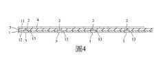
參閱圖2~4,該等第一導接線5以導電材料製成,分別貫穿該載板1,並連接該等第一感測線2與該處理晶片7,使該處理晶片7能施加電性訊號與掃描該等第一感測線2。實施上,該載板1還具有多個相間隔且貫穿該第一表面11與該第二表面12的第一穿孔13,該等第一導接線5分別從該等第一感測線2經該等第一穿孔13後,再以薄膜形式形成於該載板1的第二表面12,並延伸至該處理晶片7,使得該等第一感測線2利用該等第一導接線5訊號連接於該處理晶片7。Referring to FIGS. 2 to 4 , the first
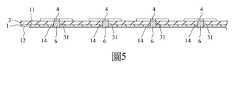
參閱圖2、圖3、圖5,該等第二導接線6以導電材料製成,分別貫穿該介電膜3與該載板1,並連接該等第二感測線4與該處理晶片7,使該處理晶片7能施加電性訊號與掃描該等第二感測線4。實施上,該載板1還具有多個相間隔且貫穿該第一表面11與該第二表面12的第二穿孔14,該介電膜3具有多個相間隔且位置分別對應該等第二穿孔14的第三穿孔31,且每一第二導接線6分別從各自的第二感測線4經各自的第三穿孔31與各自的第二穿孔14後,再以薄膜形式形成於該載板1的第二表面12,並延伸至該處理晶片7,使得該等第二感測線4利用該等第二導接線6訊號連接於該處理晶片7。Referring to FIG. 2 , FIG. 3 , and FIG. 5 , the second
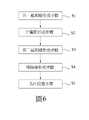
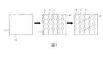
參閱圖6~8,本發明可撓式感測裝置的第一實施例的製作方法的一實施例包括一第一感測線形成步驟S1、一介電膜3形成步驟S2、一第二感測線形成步驟S3、一導接線形成步驟S4,及一晶片設置步驟S5。Referring to FIGS. 6-8 , an embodiment of the manufacturing method of the first embodiment of the flexible sensing device of the present invention includes a first sensing line forming step S1 , a
首先,進行該第一感測線形成步驟S1。先利用一氣相沉積技術(例如:一濺鍍技術)在上述的該載板1的第一表面11形成一第一金屬層;之後,再利用一微影技術與一蝕刻技術,移除該第一金屬層不需要的部分,使其下方的載板1裸露出來,而在該載板1的該第一表面11形成該等第一感測線2。可選擇地,該等第一感測線2也可以直接黏貼於該載板1上。First, the first sensing line forming step S1 is performed. First, a first metal layer is formed on the above-mentioned
之後,進行該介電膜形成步驟S2。以一塗布技術或該氣相沉積技術,在該等第一感測線2之反向於該載板1的表面上形成一介電材料,並經該介電材料硬化之後,形成該介電膜3。硬化過程可依據該介電膜3材質,透過乾燥硬化、照光硬化,或加熱硬化。After that, the dielectric film forming step S2 is performed. A dielectric material is formed on the surface of the
再來,進行該第二感測線形成步驟S3。先利用該氣相沉積技術(例如:該濺鍍技術),在該介電膜3上形成一第二金屬層;之後,再利用該微影技術與該蝕刻技術,移除該第二金屬層不需要的部分,使其下方的介電膜3裸露出來,而形成該等第二感測線4,且每一第二感測線4透過該介電膜3而與該等第一感測線2間隔相交。可選擇地,該等第二感測線4也可以直接黏貼於該載板1上。Next, the second sensing line forming step S3 is performed. First use the vapor deposition technique (eg, the sputtering technique) to form a second metal layer on the
而後,進行該導接線形成步驟S4。參閱圖4、圖5與圖8,先形成貫穿該載板1的第一表面11與第二表面12並分別連接該等第一感測線2與該處理晶片7的該等第一導接線5,及貫穿該載板1的第一表面11與第二表面12並分別連接該等第二感測線4與該處理晶片7的該等第二導接線6。在實施上,可在該載板1鑽有所述第一穿孔13與第二穿孔14,並在該介電膜3形成所述第三穿孔31,每一第一穿孔13位置對應各自的第一感測線2的其中一端部,每一第二穿孔14位置對應各自的第三穿孔31,且位置對應各自的第二感測線4的其中一端部;並於該等第一穿孔13、該等第二穿孔14及該等第三穿孔31中填入導電材料,而成為該等第一導接線5與該等第二導接線6的其中一部分;最後,再於該載板1的第二表面12形成該等第一導接線5與該等第二導接線6其餘部分,而完成該等第一感測線2與該等第二感測線4的製作。當然,也可在形成該等第一感測線2與該等第二感測線4之前,就先在該載板1鑽設形成該等該等第一穿孔13與該等第二穿孔14;或先進行該導接線形成步驟S4,再進行該第一感測線形成步驟S1、該介電膜形成步驟S2與該第二感測線形成步驟S3視實際製程需求決定。Then, the conductive line forming step S4 is performed. Referring to FIG. 4 , FIG. 5 and FIG. 8 , firstly form the first
參閱圖6與圖8,最後,進行該晶片設置步驟S5。利用一覆晶技術,在該載板1的第二表面12黏合並封裝該處理晶片7,而完成該可撓式感測裝置的製作。Referring to FIG. 6 and FIG. 8 , finally, the wafer setting step S5 is performed. Using a flip chip technology, the
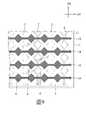
參閱圖9,為本發明可撓式感測裝置的一第二實施例,該第二實施例與該第一實施例相似,其不同處在於:該載板1的第一表面11的部分區域不被該介電膜3與該等第一感測線2覆蓋而裸露出來,且每一第二感測線4還沿該第一方向D1延伸而形成於該載板1的第一表面11之外露於該介電膜3的區域。此外,該載板1的該等第二穿孔14能自該介電膜3裸露出來,使得該等第二導接線6能自對應的第二感測線4直接穿經該載板1之後,再連接至該處理晶片7。因此,本實施例不需要在該介電膜3上設置所述第三穿孔31(如圖5),進而能在製造方法中減少一道在該介電膜3上形成所述第三穿孔31的步驟。Referring to FIG. 9 , it is a second embodiment of the flexible sensing device of the present invention. The second embodiment is similar to the first embodiment, and the difference lies in: a partial area of the
綜上所述,本發明可撓式感測裝置,利用該載板1為可撓式載板的設計,使裝置整體也為可撓式,能適度撓曲,增加設計與使用時的彈性,且本發明可撓式感測裝置的製造方法也可不限定於必須使用配合矽基板的特定半導體製程,故確實能達成本發明之目的。To sum up, the flexible sensing device of the present invention utilizes the design of the
惟以上所述者,僅為本發明之實施例而已,當不能以此限定本發明實施之範圍,凡是依本發明申請專利範圍及專利說明書內容所作之簡單的等效變化與修飾,皆仍屬本發明專利涵蓋之範圍內。However, the above are only examples of the present invention, and should not limit the scope of the present invention. Any simple equivalent changes and modifications made according to the scope of the application for patent of the present invention and the content of the patent specification are still within the scope of the present invention. within the scope of the invention patent.
1:載板1: carrier board
11:第一表面11: The first surface
12:第二表面12: Second surface
13:第一穿孔13: The first piercing
14:第二穿孔14: Second perforation
2:第一感測線2: The first sensing line
21:第一擴大部21: The first expansion
22:第一感測部22: The first sensing part
3:介電膜3: Dielectric film
31:第三穿孔31: Third Piercing
4:第二感測線4: The second sensing line
41:第二擴大部41: Second Division
42:第二感測部42: Second sensing part
5:第一導接線5: The first lead wire
6:第二導接線6: Second lead wire
7:處理晶片7: Process the wafer
D1:第一方向D1: first direction
D2:第一方向D2: first direction
S1:第一感測線形成步驟S1: the first sensing line forming step
S2:介電膜形成步驟S2: Dielectric film forming step
S3:第二感測線形成步驟S3: the second sensing line forming step
S4:導接線形成步驟S4: Lead wire forming step
S5:晶片設置步驟S5: Wafer Setting Step
本發明之其他的特徵及功效,將於參照圖式的實施方式中清楚地呈現,其中: 圖1是一俯視示意圖,說明本發明可撓式感測裝置的一第一實施例; 圖2是一仰視示意圖,說明該第一實施例; 圖3是一立體分解示意圖,說明該第一實施例; 圖4是一沿圖1中的Ⅳ-Ⅳ線所截取的一剖視圖; 圖5一沿圖1中的V-V線所截取的一剖視圖; 圖6是一流程圖,說明本發明可撓式感測裝置的該第一實施例的製造方法的一實施例; 圖7~圖8是本發明該可撓式感測裝置的製造方法的實施例的流程示意圖;及 圖9是一俯視示意圖,說明本發明可撓式感測裝置的一第二實施例。Other features and effects of the present invention will be clearly presented in the embodiments with reference to the drawings, wherein: FIG. 1 is a schematic top view illustrating a first embodiment of the flexible sensing device of the present invention; Figure 2 is a schematic bottom view illustrating the first embodiment; 3 is a schematic exploded perspective view illustrating the first embodiment; Fig. 4 is a sectional view taken along line IV-IV in Fig. 1; Figure 5-a cross-sectional view taken along the V-V line in Figure 1; FIG. 6 is a flow chart illustrating an embodiment of the manufacturing method of the first embodiment of the flexible sensing device of the present invention; 7 to 8 are schematic flowcharts of embodiments of the manufacturing method of the flexible sensing device of the present invention; and FIG. 9 is a schematic top view illustrating a second embodiment of the flexible sensing device of the present invention.
1:載板1: carrier board
11:第一表面11: The first surface
12:第二表面12: Second surface
13:第一穿孔13: The first piercing
14:第二穿孔14: Second perforation
2:第一感測線2: The first sensing line
21:第一擴大部21: The first expansion
22:第一感測部22: The first sensing part
3:介電膜3: Dielectric film
31:第三穿孔31: Third Piercing
4:第二感測線4: The second sensing line
41:第二擴大部41: Second Division
42:第二感測部42: Second sensing part
7:處理晶片7: Process the wafer
D1:第一方向D1: first direction
D2:第一方向D2: first direction
Claims (6)
Translated fromChinesePriority Applications (4)
| Application Number | Priority Date | Filing Date | Title |
|---|---|---|---|
| TW110127155ATWI778721B (en) | 2021-07-23 | 2021-07-23 | Flexible sensing device and manufacturing method thereof |
| CN202210484174.4ACN115690860A (en) | 2021-07-23 | 2022-05-06 | Flexible sensing device and manufacturing method thereof |
| US17/812,731US20230023809A1 (en) | 2021-07-23 | 2022-07-15 | Flexible sensing device and method of making the same |
| EP22185944.0AEP4123602A1 (en) | 2021-07-23 | 2022-07-20 | Flexible sensing device and method of making the same |
Applications Claiming Priority (1)
| Application Number | Priority Date | Filing Date | Title |
|---|---|---|---|
| TW110127155ATWI778721B (en) | 2021-07-23 | 2021-07-23 | Flexible sensing device and manufacturing method thereof |
Publications (2)
| Publication Number | Publication Date |
|---|---|
| TWI778721Btrue TWI778721B (en) | 2022-09-21 |
| TW202305564A TW202305564A (en) | 2023-02-01 |
Family
ID=82656458
Family Applications (1)
| Application Number | Title | Priority Date | Filing Date |
|---|---|---|---|
| TW110127155ATWI778721B (en) | 2021-07-23 | 2021-07-23 | Flexible sensing device and manufacturing method thereof |
Country Status (4)
| Country | Link |
|---|---|
| US (1) | US20230023809A1 (en) |
| EP (1) | EP4123602A1 (en) |
| CN (1) | CN115690860A (en) |
| TW (1) | TWI778721B (en) |
Citations (5)
| Publication number | Priority date | Publication date | Assignee | Title |
|---|---|---|---|---|
| TW201349060A (en)* | 2012-05-23 | 2013-12-01 | Ind Tech Res Inst | Bending detection method and bendable touch panel |
| TW201401147A (en)* | 2012-06-27 | 2014-01-01 | Univ Nat Taiwan | Fibrous material based flexible tactile sensing cell from contact mechanism |
| US20140362304A1 (en)* | 2013-06-10 | 2014-12-11 | Samsung Display Co., Ltd. | Flat panel display device |
| TW201616309A (en)* | 2014-10-21 | 2016-05-01 | 宸鴻科技(廈門)有限公司 | Touching-sensitive device and production method thereof |
| US20170228086A1 (en)* | 2016-02-05 | 2017-08-10 | Superc-Touch Corporation | Sensing device for force and tactile-proximity sensing |
Family Cites Families (4)
| Publication number | Priority date | Publication date | Assignee | Title |
|---|---|---|---|---|
| US7439962B2 (en)* | 2005-06-01 | 2008-10-21 | Synaptics Incorporated | Touch pad with flexible substrate |
| US20110012845A1 (en)* | 2009-07-20 | 2011-01-20 | Rothkopf Fletcher R | Touch sensor structures for displays |
| JP5710837B2 (en)* | 2011-06-20 | 2015-04-30 | シナプティクス インコーポレイテッド | Touch and display device with integrated sensor controller |
| JP6142745B2 (en)* | 2013-09-10 | 2017-06-07 | ソニー株式会社 | Sensor device, input device and electronic apparatus |
- 2021
- 2021-07-23TWTW110127155Apatent/TWI778721B/enactive
- 2022
- 2022-05-06CNCN202210484174.4Apatent/CN115690860A/enactivePending
- 2022-07-15USUS17/812,731patent/US20230023809A1/enactivePending
- 2022-07-20EPEP22185944.0Apatent/EP4123602A1/ennot_activeWithdrawn
Patent Citations (5)
| Publication number | Priority date | Publication date | Assignee | Title |
|---|---|---|---|---|
| TW201349060A (en)* | 2012-05-23 | 2013-12-01 | Ind Tech Res Inst | Bending detection method and bendable touch panel |
| TW201401147A (en)* | 2012-06-27 | 2014-01-01 | Univ Nat Taiwan | Fibrous material based flexible tactile sensing cell from contact mechanism |
| US20140362304A1 (en)* | 2013-06-10 | 2014-12-11 | Samsung Display Co., Ltd. | Flat panel display device |
| TW201616309A (en)* | 2014-10-21 | 2016-05-01 | 宸鴻科技(廈門)有限公司 | Touching-sensitive device and production method thereof |
| US20170228086A1 (en)* | 2016-02-05 | 2017-08-10 | Superc-Touch Corporation | Sensing device for force and tactile-proximity sensing |
Also Published As
| Publication number | Publication date |
|---|---|
| US20230023809A1 (en) | 2023-01-26 |
| TW202305564A (en) | 2023-02-01 |
| EP4123602A1 (en) | 2023-01-25 |
| CN115690860A (en) | 2023-02-03 |
Similar Documents
| Publication | Publication Date | Title |
|---|---|---|
| CN101013715B (en) | Micro heat flux sensor array | |
| US8641913B2 (en) | Fine pitch microcontacts and method for forming thereof | |
| US10891459B2 (en) | Fingerprint sensor module and method for manufacturing a fingerprint sensor module | |
| JPH04355086A (en) | Manufacture of electric connecting element | |
| JPH04345779A (en) | Manufacture of electric connecting element | |
| US11230471B2 (en) | Micro-transfer-printed compound sensor device | |
| CN205788221U (en) | There is the fingerprint acquisition apparatus of intermediary agent structure | |
| TWI549235B (en) | Package structure and method of manufacturing the same and a positioning for use in the package structure contiguration | |
| JP3687204B2 (en) | Multilayer wiring pattern forming method | |
| US20100071943A1 (en) | Package and substrate structure with at least one alignment pattern | |
| TWI778721B (en) | Flexible sensing device and manufacturing method thereof | |
| US20220246500A1 (en) | Flexible electronic structure | |
| KR100225398B1 (en) | Bonding Structure and Method of Semiconductor Bump | |
| JPS6399995A (en) | IC card and its manufacturing method | |
| JPH04340758A (en) | Semiconductor device and its manufacturing method | |
| EP3091570B1 (en) | A semiconductor power device and a method of assembling a semiconductor power device | |
| JP2001052779A (en) | Structure of contact probe and its manufacture | |
| CN111463187B (en) | Flexible device based on system-in-package and manufacturing method thereof | |
| CN111463189B (en) | System-in-package-based flexible device and its manufacturing method | |
| JPH07202115A (en) | Manufacturing of semiconductor devices | |
| CN110191567A (en) | It is aligned using physical alignment label and virtual alignment label | |
| JPH09130000A (en) | Double-sided wiring board and semiconductor device using the same | |
| JPH0290511A (en) | Semiconductor device | |
| JPS61244035A (en) | How to connect bump electrodes | |
| TWI328848B (en) | Contact structure and manufacturing method thereof |
Legal Events
| Date | Code | Title | Description |
|---|---|---|---|
| GD4A | Issue of patent certificate for granted invention patent |