TWI777733B - Light emitting diode chip and light emitting diode device - Google Patents
Light emitting diode chip and light emitting diode deviceDownload PDFInfo
- Publication number
- TWI777733B TWI777733BTW110130520ATW110130520ATWI777733BTW I777733 BTWI777733 BTW I777733BTW 110130520 ATW110130520 ATW 110130520ATW 110130520 ATW110130520 ATW 110130520ATW I777733 BTWI777733 BTW I777733B
- Authority
- TW
- Taiwan
- Prior art keywords
- semiconductor layer
- emitting diode
- light
- insulating layer
- layer
- Prior art date
Links
Images


Classifications
- H—ELECTRICITY
- H10—SEMICONDUCTOR DEVICES; ELECTRIC SOLID-STATE DEVICES NOT OTHERWISE PROVIDED FOR
- H10H—INORGANIC LIGHT-EMITTING SEMICONDUCTOR DEVICES HAVING POTENTIAL BARRIERS
- H10H20/00—Individual inorganic light-emitting semiconductor devices having potential barriers, e.g. light-emitting diodes [LED]
- H10H20/80—Constructional details
- H10H20/83—Electrodes
- H10H20/831—Electrodes characterised by their shape
- H10H20/8312—Electrodes characterised by their shape extending at least partially through the bodies
- H—ELECTRICITY
- H10—SEMICONDUCTOR DEVICES; ELECTRIC SOLID-STATE DEVICES NOT OTHERWISE PROVIDED FOR
- H10H—INORGANIC LIGHT-EMITTING SEMICONDUCTOR DEVICES HAVING POTENTIAL BARRIERS
- H10H20/00—Individual inorganic light-emitting semiconductor devices having potential barriers, e.g. light-emitting diodes [LED]
- H10H20/80—Constructional details
- H10H20/81—Bodies
- H10H20/814—Bodies having reflecting means, e.g. semiconductor Bragg reflectors
- H—ELECTRICITY
- H10—SEMICONDUCTOR DEVICES; ELECTRIC SOLID-STATE DEVICES NOT OTHERWISE PROVIDED FOR
- H10H—INORGANIC LIGHT-EMITTING SEMICONDUCTOR DEVICES HAVING POTENTIAL BARRIERS
- H10H20/00—Individual inorganic light-emitting semiconductor devices having potential barriers, e.g. light-emitting diodes [LED]
- H10H20/80—Constructional details
- H10H20/81—Bodies
- H10H20/819—Bodies characterised by their shape, e.g. curved or truncated substrates
- H—ELECTRICITY
- H10—SEMICONDUCTOR DEVICES; ELECTRIC SOLID-STATE DEVICES NOT OTHERWISE PROVIDED FOR
- H10H—INORGANIC LIGHT-EMITTING SEMICONDUCTOR DEVICES HAVING POTENTIAL BARRIERS
- H10H20/00—Individual inorganic light-emitting semiconductor devices having potential barriers, e.g. light-emitting diodes [LED]
- H10H20/80—Constructional details
- H10H20/85—Packages
- H10H20/8506—Containers
- H—ELECTRICITY
- H10—SEMICONDUCTOR DEVICES; ELECTRIC SOLID-STATE DEVICES NOT OTHERWISE PROVIDED FOR
- H10H—INORGANIC LIGHT-EMITTING SEMICONDUCTOR DEVICES HAVING POTENTIAL BARRIERS
- H10H20/00—Individual inorganic light-emitting semiconductor devices having potential barriers, e.g. light-emitting diodes [LED]
- H10H20/80—Constructional details
- H10H20/85—Packages
- H10H20/855—Optical field-shaping means, e.g. lenses
- H—ELECTRICITY
- H01—ELECTRIC ELEMENTS
- H01L—SEMICONDUCTOR DEVICES NOT COVERED BY CLASS H10
- H01L25/00—Assemblies consisting of a plurality of semiconductor or other solid state devices
- H01L25/03—Assemblies consisting of a plurality of semiconductor or other solid state devices all the devices being of a type provided for in a single subclass of subclasses H10B, H10D, H10F, H10H, H10K or H10N, e.g. assemblies of rectifier diodes
- H01L25/04—Assemblies consisting of a plurality of semiconductor or other solid state devices all the devices being of a type provided for in a single subclass of subclasses H10B, H10D, H10F, H10H, H10K or H10N, e.g. assemblies of rectifier diodes the devices not having separate containers
- H01L25/075—Assemblies consisting of a plurality of semiconductor or other solid state devices all the devices being of a type provided for in a single subclass of subclasses H10B, H10D, H10F, H10H, H10K or H10N, e.g. assemblies of rectifier diodes the devices not having separate containers the devices being of a type provided for in group H10H20/00
- H01L25/0753—Assemblies consisting of a plurality of semiconductor or other solid state devices all the devices being of a type provided for in a single subclass of subclasses H10B, H10D, H10F, H10H, H10K or H10N, e.g. assemblies of rectifier diodes the devices not having separate containers the devices being of a type provided for in group H10H20/00 the devices being arranged next to each other
- H—ELECTRICITY
- H10—SEMICONDUCTOR DEVICES; ELECTRIC SOLID-STATE DEVICES NOT OTHERWISE PROVIDED FOR
- H10H—INORGANIC LIGHT-EMITTING SEMICONDUCTOR DEVICES HAVING POTENTIAL BARRIERS
- H10H20/00—Individual inorganic light-emitting semiconductor devices having potential barriers, e.g. light-emitting diodes [LED]
- H10H20/80—Constructional details
- H10H20/84—Coatings, e.g. passivation layers or antireflective coatings
- H10H20/841—Reflective coatings, e.g. dielectric Bragg reflectors
Landscapes
- Engineering & Computer Science (AREA)
- Power Engineering (AREA)
- Microelectronics & Electronic Packaging (AREA)
- Physics & Mathematics (AREA)
- Condensed Matter Physics & Semiconductors (AREA)
- General Physics & Mathematics (AREA)
- Computer Hardware Design (AREA)
- Led Devices (AREA)
- Led Device Packages (AREA)
Abstract
Description
Translated fromChinese本揭露的一些實施方式是關於發光二極體晶片與發光二極體晶片裝置,尤其是關於發光二極體晶片與發光二極體晶片裝置的絕緣層。Some embodiments of the present disclosure relate to light emitting diode chips and light emitting diode chip devices, and more particularly, to insulating layers of light emitting diode chips and light emitting diode chip devices.
近年來,各種新型態的顯示器逐漸興起。這些顯示器大多朝向解析度增加以及節能的方向發展,微型發光二極體(micro light-emitting diode,μLED)即為其中一重要發展型態。In recent years, various new types of displays have gradually emerged. Most of these displays are developing in the direction of increased resolution and energy saving, and micro light-emitting diodes (μLEDs) are one of the important development types.
微型發光二極體將傳統發光二極體尺寸微縮至約100微米以下甚至數十微米之數量級。在此數量級下,相同面積內的發光二極體數量遽增,因此發光二極體自生長基板轉移至顯示板的良率需達99%以上。以現今之製程技術,此巨量轉移(mass transfer)尚有許多技術難題待解決。The miniature light-emitting diode reduces the size of the traditional light-emitting diode to an order of magnitude below about 100 microns or even tens of microns. Under this order of magnitude, the number of light-emitting diodes in the same area increases rapidly, so the yield of light-emitting diodes transferred from the growth substrate to the display panel needs to be over 99%. With today's process technology, there are still many technical problems to be solved in this mass transfer.
本揭露的一些實施方式為一種發光二極體晶片,包含半導體層、絕緣層、第一電極及第二電極。半導體層具有側壁與相對的頂側與底側,側壁連接頂側及底側,且半導體層的頂側上具有凹凸結構。絕緣層覆蓋半導體層的側壁與底側,其中絕緣層具有突出部,突出部沿平行側壁之方向延伸突出於凹凸結構,凹凸結構的最高點與突出部的最高點之間的垂直距離大於0.5微米且小於4倍的半導體層的厚度。第一電極在半導體層的底側上且貫穿絕緣層。第二電極與第一電極相鄰,在半導體層的底側上且貫穿絕緣層。Some embodiments of the present disclosure are a light emitting diode wafer including a semiconductor layer, an insulating layer, a first electrode and a second electrode. The semiconductor layer has sidewalls and opposite topsides and bottomsides, the sidewalls connect the topside and the bottomside, and the topside of the semiconductor layer has a concave-convex structure. The insulating layer covers the sidewall and the bottom side of the semiconductor layer, wherein the insulating layer has protrusions, the protrusions extend along the direction parallel to the sidewalls and protrude beyond the concave-convex structure, and the vertical distance between the highest point of the concave-convex structure and the highest point of the protrusion is greater than 0.5 microns And less than 4 times the thickness of the semiconductor layer. The first electrode is on the bottom side of the semiconductor layer and penetrates the insulating layer. The second electrode is adjacent to the first electrode, on the bottom side of the semiconductor layer and through the insulating layer.
在一些實施方式中,絕緣層的突出部於垂直側壁之方向上的厚度在0.4微米至3.5微米之間。In some embodiments, the thickness of the protrusions of the insulating layer in the direction perpendicular to the sidewalls is between 0.4 microns and 3.5 microns.
在一些實施方式中,突出部的最高點與凹凸結構的中心點形成連線,連線與半導體層的水平截面形成第一角度,第一角度在1度至10度的範圍之間。In some embodiments, the highest point of the protrusion and the center point of the concave-convex structure form a connection line, and the connection line forms a first angle with the horizontal section of the semiconductor layer, and the first angle is in the range of 1 degree to 10 degrees.
在一些實施方式中,絕緣層的突出部的上表面為平面。In some embodiments, the upper surface of the protrusion of the insulating layer is flat.
在一些實施方式中,絕緣層的突出部的上表面向半導體層傾斜。In some embodiments, the upper surface of the protrusion of the insulating layer is inclined toward the semiconductor layer.
在一些實施方式中,上表面與半導體層的水平截面形成第二角度,凹凸結構的表面與半導體層的水平截面形成第三角度,第二角度小於第三角度。In some embodiments, the upper surface forms a second angle with the horizontal cross-section of the semiconductor layer, the surface of the concave-convex structure forms a third angle with the horizontal cross-section of the semiconductor layer, and the second angle is smaller than the third angle.
在一些實施方式中,突出部為封閉環狀,且沿半導體層周緣設置以環繞半導體層。In some embodiments, the protrusions are closed annular and disposed along the perimeter of the semiconductor layer to surround the semiconductor layer.
在一些實施方式中,突出部為包含至少一個開口的非封閉環狀,且沿半導體層周緣設置以環繞半導體層。In some embodiments, the protrusion is a non-closed annular shape including at least one opening, and is disposed along the periphery of the semiconductor layer to surround the semiconductor layer.
在一些實施方式中,突出部包含至少一對子突出部,至少一對子突出部以半導體層的幾何中心點對稱地設置於半導體層周緣上。In some embodiments, the protruding portion includes at least a pair of sub-protrusions, and the at least one pair of sub-protrusions are point-symmetrically disposed on the periphery of the semiconductor layer with a geometric center of the semiconductor layer.
在一些實施方式中,絕緣層可反射半導體層發出的光。In some embodiments, the insulating layer can reflect light emitted by the semiconductor layer.
在一些實施方式中,絕緣層包含分布式布拉格反射器。In some embodiments, the insulating layer includes a distributed Bragg reflector.
在一些實施方式中,絕緣層的材料包含氧化層、氮化層或其組合。In some embodiments, the material of the insulating layer includes an oxide layer, a nitride layer, or a combination thereof.
本揭露的一些實施方式為一種發光二極體晶片裝置,包含載板及複數個發光二極體晶片。複數個發光二極體晶片排列在載板上。Some embodiments of the present disclosure are a light-emitting diode chip device including a carrier and a plurality of light-emitting diode chips. A plurality of light emitting diode chips are arranged on the carrier board.
本揭露中的絕緣層的突出部可以減少發光二極體晶片與膠材的接觸面積,進而減少兩者之間的黏著力。因此,在轉移發光二極體晶片時,發光二極體晶片不會因為發光二極體晶片與膠材之間過大的黏著力而無法完全分離,使得轉移發光二極體晶片的成功率可提升。The protruding portion of the insulating layer in the present disclosure can reduce the contact area between the light-emitting diode chip and the adhesive material, thereby reducing the adhesive force between the two. Therefore, when transferring the light-emitting diode chip, the light-emitting diode chip will not be completely separated due to the excessive adhesive force between the light-emitting diode chip and the adhesive material, so that the success rate of transferring the light-emitting diode chip can be improved .
為了使本揭露內容的敘述更加詳盡與完備,下文針對了本揭露的實施態樣與具體實施例提出了說明性的描述;但這並非實施或運用本揭露具體實施例的唯一形式。以下所揭露的各實施例,在有益的情形下可相互組合或取代,也可在一實施例中附加其他的實施例,而無須進一步的記載或說明。In order to make the description of the present disclosure more detailed and complete, the following provides an illustrative description for the implementation aspects and specific embodiments of the present disclosure; but this is not the only form of implementing or using the specific embodiments of the present disclosure. The embodiments disclosed below can be combined or substituted with each other under beneficial circumstances, and other embodiments can also be added to one embodiment without further description or explanation.
能理解的是,雖然在此可使用用語「第一」、「第二」、「第三」等來敘述各種元件、組成成分、區域、層、及/或部分,這些元件、組成成分、區域、層、及/或部分不應被這些用語限定,且這些用語僅是用來區別不同的元件、組成成分、區域、層、及/或部分。因此,以下討論的一第一元件、組成成分、區域、層、及/或部分可在不偏離本發明之教示的情況下被稱為一第二元件、組成成分、區域、層、及/或部分。It will be understood that although the terms "first," "second," "third," etc. may be used herein to describe various elements, components, regions, layers, and/or sections, these elements, components, regions , layer, and/or section should not be limited by these terms, and these terms are only used to distinguish between different elements, components, regions, layers, and/or sections. Thus, a first element, component, region, layer, and/or section discussed below could be termed a second element, component, region, layer, and/or section without departing from the teachings of the present invention part.
在以下描述中,將詳細敘述許多特定細節以使讀者能夠充分理解以下的實施例。然而,可在無此等特定細節之情況下實踐本揭露之實施例。在其他情況下,為簡化圖式,熟知的結構與裝置僅示意性地繪示於圖中。In the following description, numerous specific details are set forth in detail to enable the reader to fully understand the following embodiments. However, embodiments of the present disclosure may be practiced without these specific details. In other instances, well-known structures and devices are shown schematically in the drawings for simplicity of illustration.
本揭露的一些實施方式可改善轉移發光二極體晶片的良率。具體而言,本揭露的一些實施方式的發光二極體晶片的絕緣層具有從半導體層突出的突出部,因此當使用包含膠材的轉移載板轉移發光二極體晶片時,發光二極體晶片可藉由突出部插入膠材,藉此降低發光二極體晶片與膠材接觸的範圍,使得發光二極體晶片與膠材之間的附著力大小適中。因此,發光二極體晶片在轉移過程中可以順利脫離膠材,從而提升轉移發光二極體晶片的良率。Some embodiments of the present disclosure may improve the yield of transferred LED wafers. Specifically, the insulating layer of the light-emitting diode wafer of some embodiments of the present disclosure has protrusions protruding from the semiconductor layer, so when the light-emitting diode wafer is transferred using a transfer carrier containing a glue material, the light-emitting diode wafer The chip can be inserted into the glue material through the protruding portion, thereby reducing the contact range between the light emitting diode chip and the glue material, so that the adhesion between the light emitting diode chip and the glue material is moderate. Therefore, the light emitting diode wafer can be smoothly released from the adhesive material during the transfer process, thereby improving the yield of the transferred light emitting diode wafer.
第1A圖至第14圖繪示根據本揭露的一些實施方式的製造包含發光二極體晶片100的發光二極體裝置200的製程。參考第1A圖,在晶圓102上形成半導體層110。晶圓102的上表面102a為凹凸表面,因此在半導體層110形成在晶圓102上時,半導體層110與晶圓102之間會形成凹凸界面。在一些實施方式中,可在半導體層110與晶圓102之間另外形成共形的聚合物層104,如第1B圖所示。因此,聚合物層104與晶圓102之間也會形成凹凸界面。FIGS. 1A through 14 illustrate a process of fabricating a light-emitting
在一些實施方式中,晶圓102可包含半導體、矽、藍寶石或類似者。在一些實施方式中,半導體層110可至少包含第一半導體層、主動層與第二半導體層(可對應至第15圖中的第一半導體層114、主動層116與第二半導體層118)。在一些實施方式中,第一半導體層可為N型摻雜氮化鎵,主動層可為加入量子井結構與/或量子點結構的氮化鎵,且第二半導體層可為P型摻雜氮化鎵。半導體層110也可由其他適合的材料製成。In some embodiments,
參考第2圖,進行蝕刻製程蝕刻半導體層110,以在半導體層110中形成凹槽112。在一些實施方式中,可進行適合的蝕刻製程,例如乾式蝕刻或濕式蝕刻,來形成凹槽112。凹槽112定義出後續形成的電極(如第5圖的第一電極131)的位置。Referring to FIG. 2 , an etching process is performed to etch the
參考第3圖,進一步部分地蝕刻半導體層110,以在半導體層110中形成複數個溝槽T。相鄰的溝槽T定義出一個圖案化半導體層110’與後續形成的發光二極體晶片(如第15圖的發光二極體晶片100)的側壁(如第15圖的側壁111a)。在第3圖中,僅部分地蝕刻半導體層110,意即半導體層110的底部仍相連,且第3圖的蝕刻製程不會蝕刻晶圓102。Referring to FIG. 3 , the
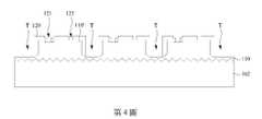
參考第4圖,蝕刻半導體層110後,在半導體層110上共形地形成絕緣層120,並在絕緣層120中形成第一電極孔121與第二電極孔122。第一電極孔121位於凹槽112的上方。因此,第一電極孔121的位置比第二電極孔122低。在一些實施方式中,第一電極孔121暴露半導體層110的第一半導體層(如第15圖的第一半導體層114),且第二電極孔122暴露半導體層110的第二半導體層(如第15圖的第二半導體層118)。在一些實施方式中,絕緣層120包含氧化層、氮化層或其組合。Referring to FIG. 4 , after etching the
參考第5圖,在第一電極孔121與第二電極孔122中形成第一電極131與第二電極132。可用任何適合的導電材料,例如金屬,形成第一電極131與第二電極132。第一電極131與第二電極132連接至圖案化半導體層110’中的不同位置,例如,圖案化半導體層110’中不同類型的半導體層(將在第15圖中詳細描述)。Referring to FIG. 5 , a
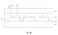
參考第6圖,在第5圖所示的結構上依序形成犧牲層142與第一載板144。犧牲層142可為任何適合的介電材料,且與絕緣層120之間有蝕刻選擇性的材料。第一載板144則由與晶圓102相似或相同的材料製成。接著,在第7圖中,翻轉第6圖中所示的結構,使得第一載板144在整個結構的最底部。Referring to FIG. 6 , the
參考第8圖,移除晶圓102。可使用蝕刻製程、雷射剝離(Laser-Lift-Off)製程、或其它適合的方式來移除晶圓102。由於圖案化半導體層110’與晶圓102之間具有凹凸界面,因此在移除晶圓102之後,圖案化半導體層110’具有凹凸結構113。當後續形成的發光二極體晶片(如第15圖中的發光二極體晶片100)具有凹凸結構113,可以減少光的全反射而增加光萃取率。Referring to FIG. 8, the
參考第9圖,移除部分的圖案化半導體層110’,使得圖案化半導體層110’的高度低於絕緣層120的高度,並形成絕緣層120的突出部124。絕緣層120的突出部124突出於圖案化半導體層110’的凹凸結構113,且可用於在後續的轉移製程中,增加晶片轉移的良率。可利用任何適合的蝕刻製程移除部分的圖案化半導體層110’。由於在第9圖的移除製程以實質上相同的速率由上往下移除部分的圖案化半導體層110’,因此在移除製程後,圖案化半導體層110’仍具有凹凸結構113。在移除部分的圖案化半導體層110’的同時或是之後,可圖案化絕緣層120的突出部124,使得絕緣層120的突出部124具有不同的俯視圖案。Referring to FIG. 9, a portion of the patterned semiconductor layer 110' is removed, so that the height of the patterned semiconductor layer 110' is lower than that of the insulating
在圖案化半導體層110’上具有聚合物層的實施方式中(例如,從第1B圖發展的實施方式),移除部分的聚合物層104(第1B圖),使得絕緣層120的突出部124突出於圖案化半導體層110’的凹凸結構113。因此在此實施方式中,凹凸結構113也可包含聚合物層104(第19圖)。In embodiments having a polymer layer on the patterned
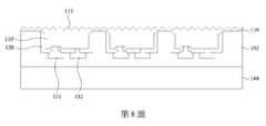
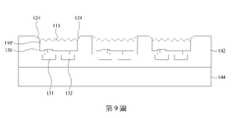
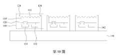
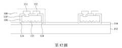
參考第10圖,移除部分的犧牲層142。具體而言,沿著絕緣層120的外表面垂直地(非等向性地)移除犧牲層142,並形成各自獨立的發光二極體晶片100。接著,參考第11圖,再次將第10圖的結構翻轉後,將第一載板144上的發光二極體晶片100轉移至第二載板152上。第二載板152上塗佈有膠材154。在轉移發光二極體晶片100的過程中,絕緣層120的突出部124容易刺入膠材154並固定在膠材154上。因突出部124高於圖案化半導體層110’的頂側,因此圖案化半導體層110’的頂側可能會不接觸膠材154,或者僅部分接觸膠材154。不論如何,圖案化半導體層110’的頂側與膠材154之間的附著力因接觸面積的減少而降低,而發光二極體晶片100主要藉由絕緣層120的突出部124固定於膠材154上。另外,轉移製程可針對不同的需求而選擇性地將部分的發光二極體晶片100放置在膠材154上。舉例而言,如第11圖所示,此轉移製程將部分的發光二極體晶片100放置在膠材154上,而另一部分的發光二極體晶片100仍留在第一載板144上。接著,移除剩餘的犧牲層142,如第12圖所示。Referring to FIG. 10, a portion of the
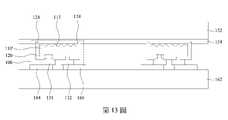
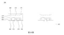
參考第13圖,翻轉第二載板152,並將第二載板152上的發光二極體晶片100轉移至第三載板162。在一些實施方式中,第三載板162為電路板,且第三載板162上設置有接觸墊164與166。在轉移發光二極體晶片100時,接觸墊164與166分別連接至第一電極131與第二電極132以分別與第一電極131與第二電極132電性連接。如上所述,由於絕緣層120的突出部124從圖案化半導體層110’突出,當絕緣層120的突出部124刺入第二載板152上的膠材154時,圖案化半導體層110’與膠材154的接觸面積很小,圖案化導體層110’與膠材154之間的附著力也較小。將發光二極體晶片100轉移至第三載板162時,較小的附著力使得圖案化半導體層110’容易從膠材154剝離並轉移至第三載板162,而不損害發光二極體晶片100的圖案化半導體層110’。轉移至第三載板162的複數個發光二極體晶片100排列在第三載板162上,可形成用於後續應用的發光二極體晶片裝置200,如第14圖所示。Referring to FIG. 13 , the
第15圖繪示第14圖的發光二極體晶片100的放大圖。在第15圖中,發光二極體晶片100包含圖案化半導體層110’、絕緣層120、第一電極131與第二電極132。圖案化半導體層110’具有側壁111a、相對的頂側111b與底側111c。側壁111a連接頂側111b與底側111c,且頂側111b上具有凹凸結構113。凹凸結構113可為規則的或不規則的。在一些實施方式中,圖案化半導體層110’為多層結構,並包含由上而下的第一半導體層114、主動層116與第二半導體層118。第一半導體層114具有第一型半導體材料,例如n型,第二半導體層118則具有與第一型半導體材料不同型的第二半導體材料,例如p型。主動層116可為加入量子井結構與/或量子點結構的層,因此當電流通過主動層116時,主動層116可發出特定的光。FIG. 15 is an enlarged view of the light emitting
絕緣層120覆蓋圖案化半導體層110’的側壁111a與底側111c。在一些實施方式中,絕緣層120可以被圖案化半導體層110’的主動層116發出的光穿透,以獲得具有大出光角度的光形。在一些實施方式中,絕緣層120可反射從圖案化半導體層110’的主動層116發出的光,以獲得集中於正向出光的光形。在一些實施方式中,絕緣層120包含分布式布拉格反射器。絕緣層120具有突出部124,突出部124沿平行側壁111a的方向延伸突出於凹凸結構113。具有絕緣層120的突出部124的發光二極體晶片100容易藉由突出部124固定在第11圖中的膠材154。再者,絕緣層120的突出部124的存在降低膠材154與發光二極體晶片100之間的附著力,因此在轉移發光二極體晶片100至第三載板162(參考第13圖)時,不會因過大的附著力使得發光二極體晶片100被膠材154損壞、沾黏或是無法脫離膠材154,以增加轉移發光二極體晶片100的良率。在一些實施方式中,絕緣層120的厚度T1在約0.4微米至約3.5微米的範圍內。若絕緣層120的厚度T1落於所揭露的範圍外,則絕緣層120的突出部124不易刺入膠材154,使得發光二極體晶片100不易固定在膠材154上。The insulating
在一些實施方式中,凹凸結構113的最高點與突出部124的最高點之間具有垂直距離D1,且垂直距離D1在大於0.5微米且小於4倍的圖案化半導體層110’厚度T2之間。在另一些實施方式中,突出部124的最高點與凹凸結構113的中心點C形成連線L1,連線L1與圖案化半導體層110’的水平截面HL形成第一角度α1,第一角度α1在1度至10度的範圍之間。當絕緣層120可反射主動層116發出的光時,可藉此將發光二極體晶片100的出光角限制在預設的範圍內,例如約小於120度。在一些實施方式中,圖案化半導體層110’的水平截面可以是第一半導體層114與主動層116的交界面或第二半導體層118與主動層116的交界面。In some embodiments, there is a vertical distance D1 between the highest point of the concave-
在一些實施方式中,突出部124的上表面向圖案化半導體層110’傾斜。可根據不同情況決定突出部124的上表面的傾斜程度,例如當膠體154黏度較大時,較大的傾斜程度可以使突出部124更容易穿進膠體154中。在一些實施方式中,突出部124的上表面的延伸線L2與圖案化半導體層110’的水平截面形成第二角度α2,凹凸結構113的任一表面的延伸線L3與圖案化半導體層110’的水平截面形成第三角度α3,且第二角度α2小於第三角度α3。當第二角度α2小於第三角度α3,且絕緣層120的突出部124可反射從凹凸結構113射出的光時,可使發光二極體晶片100的光集中向上射出。In some embodiments, the upper surfaces of the
第一電極131與第二電極132位於圖案化半導體層110’的底側111c,且第二電極132與第一電極131相鄰。第一電極131貫穿絕緣層120並與第一半導體層114接觸,而第二電極131貫穿絕緣層120並與第二半導體層118接觸。第一電極131與第二電極132可進一步分別與第三載板162上的接觸墊164、166電性連接。The
絕緣層120的突出部124亦可具有不同的形狀。舉例而言,突出部124的上表面可為平面,如第16圖所示,其繪示根據本揭露的一些實施方式的發光二極體晶片100的剖面圖。在第16圖中,突出部124的上表面可實質平行於水平截面HL。至於第16圖的發光二極體晶片100的其他細節皆與第15圖的發光二極體晶片100相同或相似,因此便不再贅述。The
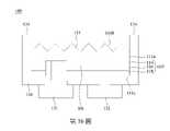
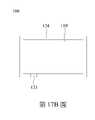
第17A圖至第18B圖繪示根據本揭露的一些實施方式的發光二極體晶片100的上視圖。在一些實施方式中,絕緣層120的突出部124也可具有不同的俯視圖案。舉例而言,在第17A圖中,絕緣層120的突出部124為封閉環狀,且沿圖案化半導體層110’的周緣設置以環繞圖案化半導體層110’。在第17B圖中,絕緣層120的突出部124為包含至少一個開口123的非封閉環狀,且沿圖案化半導體層110’周緣設置以環繞圖案化半導體層110’。應注意開口123的位置不侷限於如第17B圖所示的位置上。舉例而言,開口123可位於突出部124的較長邊處,如第17B圖所示。開口123也可位於突出部124的較短邊處。開口123暴露底下的絕緣層120,意即在開口123中,絕緣層120的開口123底部與圖案化半導體層110’的頂側111b的高度相同。在一些實施方式中,絕緣層120的突出部124也可包含至少一對子突出部126,如第18A圖與第18B圖所示。子突出部126可具有任何適合的形狀,例如矩形(第18A圖)、圓形(第18B圖)或其他合適的形狀等。每對子突出部126以圖案化半導體層110’的幾何中心P點對稱地設置於圖案化半導體層110’周緣上。子突出部126的大小足夠穿入膠材154並提供與膠材154之間的附著力,而不使得過多部分的發光二極體晶片100與膠材154接觸。FIGS. 17A-18B illustrate top views of a light-emitting
第19圖繪示根據本揭露的一些實施方式的發光二極體晶片100的剖面圖。在一些實施方式中,凹凸結構113也可包含聚合物。舉例而言,當發光二極體晶片100是由第1B圖所示的結構發展而成,由於聚合物層104不會在製程中完全被移除,在發光二極體晶片100的最終結構中,聚合物層104仍會在圖案化半導體層110’上。因此,凹凸結構113也可包含聚合物,如第19圖所示。FIG. 19 illustrates a cross-sectional view of a light-emitting
綜上所述,本揭露中的絕緣層的突出部可以減少發光二極體晶片與膠材的接觸面積,進而降低兩者之間的黏著力。因此,在轉移發光二極體晶片時,發光二極體晶片不會因為發光二極體晶片與膠材之間過大的黏著力而無法順利分離,使得轉移發光二極體晶片的成功率可提升。To sum up, the protruding portion of the insulating layer in the present disclosure can reduce the contact area between the light-emitting diode chip and the adhesive material, thereby reducing the adhesion between the two. Therefore, when transferring the light-emitting diode chip, the light-emitting diode chip will not be unable to be separated smoothly due to the excessive adhesive force between the light-emitting diode chip and the adhesive material, so that the success rate of transferring the light-emitting diode chip can be improved .
雖然本發明已以實施方式揭露如上,然其並非用以限定本發明,任何熟習此技藝者,在不脫離本發明之精神和範圍內,當可作各種之更動與潤飾,因此本發明之保護範圍當視後附之申請專利範圍所界定者為準。Although the present invention has been disclosed in the above embodiments, it is not intended to limit the present invention. Anyone skilled in the art can make various changes and modifications without departing from the spirit and scope of the present invention. Therefore, the protection of the present invention The scope shall be determined by the scope of the appended patent application.
100:發光二極體晶片 102:晶圓 102a:上表面 104:聚合物層 110:半導體層 110’:圖案化半導體層 111a:側壁 111b:頂側 111c:底側 112:凹槽 113:凹凸結構 114:第一半導體層 116:主動層 118:第二半導體層 120:絕緣層 121:第一電極孔 122:第二電極孔 123:開口 124:突出部 126:子突出部 131:第一電極 132:第二電極 142:犧牲層 144:第一載板 152:第二載板 154:膠材 162:第三載板 164:接觸墊 166:接觸墊 α1:第一角度 α2:第二角度 α3:第三角度 C:中心點 D1:垂直距離 HL:水平截面 L1:連線 L2:延伸線 L3:延伸線 P:幾何中心 T:溝槽 T1:厚度 T2:厚度100: LED chip 102:
附圖揭示出了本揭露之一個或多個實施方式,並配合說明書中的說明一起用於解釋本揭露的原理。只要有可能,與整個附圖中使用相同的標記來表示實施方式中的相同或相似的元件。其中這些附圖包含: 第1A圖至第14圖繪示根據本揭露的一些實施方式的製造包含發光二極體晶片的發光二極體裝置的製程。 第15圖繪示第14圖的發光二極體晶片的放大圖。 第16圖繪示根據本揭露的一些實施方式的發光二極體晶片的剖面圖。 第17A圖至第18B圖繪示根據本揭露的一些實施方式的發光二極體晶片的上視圖。 第19圖繪示根據本揭露的一些實施方式的發光二極體晶片的剖面圖。The accompanying drawings illustrate one or more embodiments of the present disclosure, and together with the description in the specification serve to explain the principles of the present disclosure. Wherever possible, the same reference numbers will be used throughout the drawings to refer to the same or like elements of the embodiments. These drawings include: FIGS. 1A-14 illustrate a process of fabricating a light-emitting diode device including a light-emitting diode wafer according to some embodiments of the present disclosure. FIG. 15 is an enlarged view of the light emitting diode wafer of FIG. 14 . FIG. 16 illustrates a cross-sectional view of a light emitting diode wafer according to some embodiments of the present disclosure. FIGS. 17A-18B illustrate top views of light-emitting diode chips according to some embodiments of the present disclosure. FIG. 19 illustrates a cross-sectional view of a light emitting diode wafer according to some embodiments of the present disclosure.
國內寄存資訊(請依寄存機構、日期、號碼順序註記) 無 國外寄存資訊(請依寄存國家、機構、日期、號碼順序註記) 無Domestic storage information (please note in the order of storage institution, date and number) none Foreign deposit information (please note in the order of deposit country, institution, date and number) none
100:發光二極體晶片100: LED chip
110’:圖案化半導體層110': Patterned semiconductor layer
111a:側壁111a: Sidewall
111b:頂側111b: top side
111c:底側111c: Bottom side
113:凹凸結構113: Concave and convex structure
114:第一半導體層114: first semiconductor layer
116:主動層116: Active layer
118:第二半導體層118: second semiconductor layer
120:絕緣層120: Insulation layer
124:突出部124: Protrusion
131:第一電極131: The first electrode
132:第二電極132: Second electrode
α 1:第一角度α 1: first angle
α 2:第二角度α 2: Second angle
α 3:第三角度α 3: The third angle
C:中心點C: center point
D1:垂直距離D1: vertical distance
HL:水平截面HL: Horizontal Section
L1:連線L1: connection
L2:延伸線L2: Extension Line
L3:延伸線L3: Extension Line
T1:厚度T1: Thickness
T2:厚度T2: Thickness
Claims (13)
Translated fromChinesePriority Applications (3)
| Application Number | Priority Date | Filing Date | Title |
|---|---|---|---|
| TW110130520ATWI777733B (en) | 2021-08-18 | 2021-08-18 | Light emitting diode chip and light emitting diode device |
| US17/662,658US20230057589A1 (en) | 2021-08-18 | 2022-05-10 | Light-emitting diode chip and light-emitting diode device |
| CN202210954438.8ACN115708229A (en) | 2021-08-18 | 2022-08-10 | Light emitting diode wafer and light emitting diode wafer device |
Applications Claiming Priority (1)
| Application Number | Priority Date | Filing Date | Title |
|---|---|---|---|
| TW110130520ATWI777733B (en) | 2021-08-18 | 2021-08-18 | Light emitting diode chip and light emitting diode device |
Publications (2)
| Publication Number | Publication Date |
|---|---|
| TWI777733Btrue TWI777733B (en) | 2022-09-11 |
| TW202310445A TW202310445A (en) | 2023-03-01 |
Family
ID=84958078
Family Applications (1)
| Application Number | Title | Priority Date | Filing Date |
|---|---|---|---|
| TW110130520ATWI777733B (en) | 2021-08-18 | 2021-08-18 | Light emitting diode chip and light emitting diode device |
Country Status (3)
| Country | Link |
|---|---|
| US (1) | US20230057589A1 (en) |
| CN (1) | CN115708229A (en) |
| TW (1) | TWI777733B (en) |
Citations (5)
| Publication number | Priority date | Publication date | Assignee | Title |
|---|---|---|---|---|
| TW201234574A (en)* | 2011-02-01 | 2012-08-16 | Pinecone En Inc | Light-emitting-diode array and manufacturing method thereof |
| WO2017164484A1 (en)* | 2016-03-23 | 2017-09-28 | 한국광기술원 | Led structure, transfer body, and transfer method using same |
| TW201923729A (en)* | 2017-11-15 | 2019-06-16 | 鴻海精密工業股份有限公司 | Method for preparing micro LED display panel |
| US20200303595A1 (en)* | 2017-12-11 | 2020-09-24 | Xiamen Sanan Optoelectronics Technology Co., Ltd. | Light-emitting diode and method for transferring the same |
| CN112397491A (en)* | 2020-11-16 | 2021-02-23 | 錼创显示科技股份有限公司 | Micro light-emitting diode display element and manufacturing method thereof |
Family Cites Families (5)
| Publication number | Priority date | Publication date | Assignee | Title |
|---|---|---|---|---|
| JP4989773B1 (en)* | 2011-05-16 | 2012-08-01 | 株式会社東芝 | Semiconductor light emitting device |
| JP5377725B1 (en)* | 2012-08-21 | 2013-12-25 | 株式会社東芝 | Semiconductor light emitting device |
| DE102015112538B4 (en)* | 2015-07-30 | 2023-08-03 | OSRAM Opto Semiconductors Gesellschaft mit beschränkter Haftung | Optoelectronic component and a method for producing an optoelectronic component |
| CN109860364B (en)* | 2017-08-30 | 2020-09-01 | 天津三安光电有限公司 | Light emitting diode |
| US12376428B2 (en)* | 2021-05-10 | 2025-07-29 | Xiamen San'an Optoelectronics Co., Ltd. | Micro light-emitting diode and micro light-emitting device with rough surface and protection layer |
- 2021
- 2021-08-18TWTW110130520Apatent/TWI777733B/enactive
- 2022
- 2022-05-10USUS17/662,658patent/US20230057589A1/enactivePending
- 2022-08-10CNCN202210954438.8Apatent/CN115708229A/enactivePending
Patent Citations (5)
| Publication number | Priority date | Publication date | Assignee | Title |
|---|---|---|---|---|
| TW201234574A (en)* | 2011-02-01 | 2012-08-16 | Pinecone En Inc | Light-emitting-diode array and manufacturing method thereof |
| WO2017164484A1 (en)* | 2016-03-23 | 2017-09-28 | 한국광기술원 | Led structure, transfer body, and transfer method using same |
| TW201923729A (en)* | 2017-11-15 | 2019-06-16 | 鴻海精密工業股份有限公司 | Method for preparing micro LED display panel |
| US20200303595A1 (en)* | 2017-12-11 | 2020-09-24 | Xiamen Sanan Optoelectronics Technology Co., Ltd. | Light-emitting diode and method for transferring the same |
| CN112397491A (en)* | 2020-11-16 | 2021-02-23 | 錼创显示科技股份有限公司 | Micro light-emitting diode display element and manufacturing method thereof |
Also Published As
| Publication number | Publication date |
|---|---|
| US20230057589A1 (en) | 2023-02-23 |
| TW202310445A (en) | 2023-03-01 |
| CN115708229A (en) | 2023-02-21 |
Similar Documents
| Publication | Publication Date | Title |
|---|---|---|
| JP5620269B2 (en) | Light emitting device package and manufacturing method thereof | |
| CN101515621B (en) | Light emitting diode chip, manufacturing method and packaging method | |
| CN109103315B (en) | Light emitting assembly, micro light emitting diode and display device thereof | |
| TWI664750B (en) | LED chip and manufacturing method thereof, display panel and electronic equipment | |
| WO2021087686A1 (en) | Light-emitting diode and manufacturing method therefor | |
| CN110676355B (en) | Method of making a light-emitting element | |
| US10868217B2 (en) | LED chips, method of manufacturing the same, and display panels | |
| US20250287738A1 (en) | Semiconductor chip and light-emitting device | |
| CN111933772B (en) | Light-emitting diode and method of making the same | |
| CN105518879A (en) | Light emitting element | |
| CN112310142A (en) | Display device, display panel and manufacturing method thereof | |
| TWI661584B (en) | Light emitting chip, packaged structure and associated manufacturing method | |
| TWI777733B (en) | Light emitting diode chip and light emitting diode device | |
| TW201032349A (en) | Light-emitting diode chip, and manufacturing method and packaging method therefor | |
| CN116779737A (en) | LED chip and preparation method thereof | |
| CN114883469B (en) | Light emitting diode chip for improving current conduction and preparation method thereof | |
| KR100702430B1 (en) | Light emitting diode package and manufacturing method thereof | |
| JP7317831B2 (en) | Method of manufacturing conversion element and conversion element | |
| CN102237464A (en) | Light emitting diode structure and manufacturing method thereof | |
| CN216288493U (en) | Light emitting diode | |
| CN118486771B (en) | Micro light-emitting diode display module and preparation method thereof | |
| TWI755183B (en) | Device with light-emitting diode | |
| CN114864625A (en) | Integrated LED chip and manufacturing method thereof | |
| CN118525374A (en) | Optoelectronic array and method for producing an optoelectronic array | |
| CN114093997A (en) | Large-opening-angle light emitting diode chip and manufacturing method thereof |
Legal Events
| Date | Code | Title | Description |
|---|---|---|---|
| GD4A | Issue of patent certificate for granted invention patent |