TWI776563B - Transistor and semiconductor device - Google Patents
Transistor and semiconductor deviceDownload PDFInfo
- Publication number
- TWI776563B TWI776563BTW110123203ATW110123203ATWI776563BTW I776563 BTWI776563 BTW I776563BTW 110123203 ATW110123203 ATW 110123203ATW 110123203 ATW110123203 ATW 110123203ATW I776563 BTWI776563 BTW I776563B
- Authority
- TW
- Taiwan
- Prior art keywords
- transistor
- insulator
- conductor
- semiconductor layer
- semiconductor
- Prior art date
Links
- 239000004065semiconductorSubstances0.000titleclaimsabstractdescription494
- 239000004020conductorSubstances0.000claimsabstractdescription348
- 239000012212insulatorSubstances0.000claimsabstractdescription340
- QVGXLLKOCUKJST-UHFFFAOYSA-Natomic oxygenChemical compound[O]QVGXLLKOCUKJST-UHFFFAOYSA-N0.000claimsdescription63
- 229910052760oxygenInorganic materials0.000claimsdescription63
- 239000001301oxygenSubstances0.000claimsdescription63
- 229910052782aluminiumInorganic materials0.000claimsdescription21
- XAGFODPZIPBFFR-UHFFFAOYSA-NaluminiumChemical compound[Al]XAGFODPZIPBFFR-UHFFFAOYSA-N0.000claimsdescription21
- 229910052738indiumInorganic materials0.000claimsdescription21
- APFVFJFRJDLVQX-UHFFFAOYSA-Nindium atomChemical compound[In]APFVFJFRJDLVQX-UHFFFAOYSA-N0.000claimsdescription21
- GYHNNYVSQQEPJS-UHFFFAOYSA-NGalliumChemical compound[Ga]GYHNNYVSQQEPJS-UHFFFAOYSA-N0.000claimsdescription16
- 229910052727yttriumInorganic materials0.000claimsdescription16
- VWQVUPCCIRVNHF-UHFFFAOYSA-Nyttrium atomChemical compound[Y]VWQVUPCCIRVNHF-UHFFFAOYSA-N0.000claimsdescription16
- ATJFFYVFTNAWJD-UHFFFAOYSA-NTinChemical compound[Sn]ATJFFYVFTNAWJD-UHFFFAOYSA-N0.000claimsdescription15
- 229910052733galliumInorganic materials0.000claimsdescription15
- 229910052718tinInorganic materials0.000claimsdescription15
- 239000000463materialSubstances0.000claimsdescription9
- 150000001875compoundsChemical class0.000claimsdescription8
- 230000003071parasitic effectEffects0.000abstractdescription8
- 239000010410layerSubstances0.000description157
- 238000000034methodMethods0.000description150
- 239000000758substrateSubstances0.000description109
- XUIMIQQOPSSXEZ-UHFFFAOYSA-NSiliconChemical compound[Si]XUIMIQQOPSSXEZ-UHFFFAOYSA-N0.000description56
- 229910052710siliconInorganic materials0.000description56
- 239000010703siliconSubstances0.000description56
- 238000000206photolithographyMethods0.000description50
- 238000012545processingMethods0.000description47
- 230000008569processEffects0.000description43
- 238000010438heat treatmentMethods0.000description42
- IJGRMHOSHXDMSA-UHFFFAOYSA-NAtomic nitrogenChemical compoundN#NIJGRMHOSHXDMSA-UHFFFAOYSA-N0.000description40
- 238000000231atomic layer depositionMethods0.000description40
- 239000013078crystalSubstances0.000description39
- 238000005229chemical vapour depositionMethods0.000description34
- 230000015654memoryEffects0.000description32
- 125000004429atomChemical group0.000description29
- 239000012535impuritySubstances0.000description27
- 238000001451molecular beam epitaxyMethods0.000description24
- 238000004544sputter depositionMethods0.000description22
- 229910052739hydrogenInorganic materials0.000description20
- 238000004519manufacturing processMethods0.000description20
- 229910052757nitrogenInorganic materials0.000description20
- 239000001257hydrogenSubstances0.000description19
- RYGMFSIKBFXOCR-UHFFFAOYSA-NCopperChemical compound[Cu]RYGMFSIKBFXOCR-UHFFFAOYSA-N0.000description18
- VYPSYNLAJGMNEJ-UHFFFAOYSA-NSilicium dioxideChemical compoundO=[Si]=OVYPSYNLAJGMNEJ-UHFFFAOYSA-N0.000description18
- 229910052802copperInorganic materials0.000description18
- 239000010949copperSubstances0.000description18
- 230000006870functionEffects0.000description18
- 230000015572biosynthetic processEffects0.000description17
- UFHFLCQGNIYNRP-UHFFFAOYSA-NHydrogenChemical compound[H][H]UFHFLCQGNIYNRP-UHFFFAOYSA-N0.000description16
- RTAQQCXQSZGOHL-UHFFFAOYSA-NTitaniumChemical compound[Ti]RTAQQCXQSZGOHL-UHFFFAOYSA-N0.000description16
- AJNVQOSZGJRYEI-UHFFFAOYSA-Ndigallium;oxygen(2-)Chemical compound[O-2].[O-2].[O-2].[Ga+3].[Ga+3]AJNVQOSZGJRYEI-UHFFFAOYSA-N0.000description16
- 229910001195gallium oxideInorganic materials0.000description16
- 229910052814silicon oxideInorganic materials0.000description16
- 229910052719titaniumInorganic materials0.000description16
- 239000010936titaniumSubstances0.000description16
- 239000004973liquid crystal related substanceSubstances0.000description15
- PXHVJJICTQNCMI-UHFFFAOYSA-NNickelChemical compound[Ni]PXHVJJICTQNCMI-UHFFFAOYSA-N0.000description14
- 229910052581Si3N4Inorganic materials0.000description14
- TWNQGVIAIRXVLR-UHFFFAOYSA-Noxo(oxoalumanyloxy)alumaneChemical compoundO=[Al]O[Al]=OTWNQGVIAIRXVLR-UHFFFAOYSA-N0.000description14
- HQVNEWCFYHHQES-UHFFFAOYSA-Nsilicon nitrideChemical compoundN12[Si]34N5[Si]62N3[Si]51N64HQVNEWCFYHHQES-UHFFFAOYSA-N0.000description14
- 229910052715tantalumInorganic materials0.000description14
- GUVRBAGPIYLISA-UHFFFAOYSA-Ntantalum atomChemical compound[Ta]GUVRBAGPIYLISA-UHFFFAOYSA-N0.000description14
- XKRFYHLGVUSROY-UHFFFAOYSA-NArgonChemical compound[Ar]XKRFYHLGVUSROY-UHFFFAOYSA-N0.000description12
- ZOXJGFHDIHLPTG-UHFFFAOYSA-NBoronChemical compound[B]ZOXJGFHDIHLPTG-UHFFFAOYSA-N0.000description12
- 229910052796boronInorganic materials0.000description12
- 238000010586diagramMethods0.000description12
- MRELNEQAGSRDBK-UHFFFAOYSA-Nlanthanum(3+);oxygen(2-)Chemical compound[O-2].[O-2].[O-2].[La+3].[La+3]MRELNEQAGSRDBK-UHFFFAOYSA-N0.000description12
- PLDDOISOJJCEMH-UHFFFAOYSA-Nneodymium(3+);oxygen(2-)Chemical compound[O-2].[O-2].[O-2].[Nd+3].[Nd+3]PLDDOISOJJCEMH-UHFFFAOYSA-N0.000description12
- 239000011347resinSubstances0.000description12
- 229920005989resinPolymers0.000description12
- WFKWXMTUELFFGS-UHFFFAOYSA-NtungstenChemical compound[W]WFKWXMTUELFFGS-UHFFFAOYSA-N0.000description12
- 229910052721tungstenInorganic materials0.000description12
- 239000010937tungstenSubstances0.000description12
- OAICVXFJPJFONN-UHFFFAOYSA-NPhosphorusChemical compound[P]OAICVXFJPJFONN-UHFFFAOYSA-N0.000description11
- QCWXUUIWCKQGHC-UHFFFAOYSA-NZirconiumChemical compound[Zr]QCWXUUIWCKQGHC-UHFFFAOYSA-N0.000description11
- 230000007547defectEffects0.000description11
- 230000005684electric fieldEffects0.000description11
- 229910052751metalInorganic materials0.000description11
- 239000002184metalSubstances0.000description11
- 229910052698phosphorusInorganic materials0.000description11
- 239000011574phosphorusSubstances0.000description11
- 239000011701zincSubstances0.000description11
- 229910052726zirconiumInorganic materials0.000description11
- PXGOKWXKJXAPGV-UHFFFAOYSA-NFluorineChemical compoundFFPXGOKWXKJXAPGV-UHFFFAOYSA-N0.000description10
- 229910052731fluorineInorganic materials0.000description10
- 239000011737fluorineSubstances0.000description10
- 229910052735hafniumInorganic materials0.000description10
- VBJZVLUMGGDVMO-UHFFFAOYSA-Nhafnium atomChemical compound[Hf]VBJZVLUMGGDVMO-UHFFFAOYSA-N0.000description10
- 238000002173high-resolution transmission electron microscopyMethods0.000description10
- WPBNNNQJVZRUHP-UHFFFAOYSA-Lmanganese(2+);methyl n-[[2-(methoxycarbonylcarbamothioylamino)phenyl]carbamothioyl]carbamate;n-[2-(sulfidocarbothioylamino)ethyl]carbamodithioateChemical compound[Mn+2].[S-]C(=S)NCCNC([S-])=S.COC(=O)NC(=S)NC1=CC=CC=C1NC(=S)NC(=O)OCWPBNNNQJVZRUHP-UHFFFAOYSA-L0.000description10
- 239000002356single layerSubstances0.000description10
- 239000007789gasSubstances0.000description9
- 229910052732germaniumInorganic materials0.000description9
- GNPVGFCGXDBREM-UHFFFAOYSA-Ngermanium atomChemical compound[Ge]GNPVGFCGXDBREM-UHFFFAOYSA-N0.000description9
- 229910000449hafnium oxideInorganic materials0.000description9
- WIHZLLGSGQNAGK-UHFFFAOYSA-Nhafnium(4+);oxygen(2-)Chemical compound[O-2].[O-2].[Hf+4]WIHZLLGSGQNAGK-UHFFFAOYSA-N0.000description9
- OKTJSMMVPCPJKN-UHFFFAOYSA-NCarbonChemical compound[C]OKTJSMMVPCPJKN-UHFFFAOYSA-N0.000description8
- HCHKCACWOHOZIP-UHFFFAOYSA-NZincChemical compound[Zn]HCHKCACWOHOZIP-UHFFFAOYSA-N0.000description8
- 229910052725zincInorganic materials0.000description8
- 229910045601alloyInorganic materials0.000description7
- 239000000956alloySubstances0.000description7
- 229910052799carbonInorganic materials0.000description7
- 229910052759nickelInorganic materials0.000description7
- -1water)Chemical compound0.000description7
- ZOKXTWBITQBERF-UHFFFAOYSA-NMolybdenumChemical compound[Mo]ZOKXTWBITQBERF-UHFFFAOYSA-N0.000description6
- 229910052779NeodymiumInorganic materials0.000description6
- 229910052786argonInorganic materials0.000description6
- 230000000903blocking effectEffects0.000description6
- YBMRDBCBODYGJE-UHFFFAOYSA-Ngermanium oxideInorganic materialsO=[Ge]=OYBMRDBCBODYGJE-UHFFFAOYSA-N0.000description6
- 229910052746lanthanumInorganic materials0.000description6
- FZLIPJUXYLNCLC-UHFFFAOYSA-Nlanthanum atomChemical compound[La]FZLIPJUXYLNCLC-UHFFFAOYSA-N0.000description6
- 229910052750molybdenumInorganic materials0.000description6
- 239000011733molybdenumSubstances0.000description6
- QEFYFXOXNSNQGX-UHFFFAOYSA-Nneodymium atomChemical compound[Nd]QEFYFXOXNSNQGX-UHFFFAOYSA-N0.000description6
- SIWVEOZUMHYXCS-UHFFFAOYSA-Noxo(oxoyttriooxy)yttriumChemical compoundO=[Y]O[Y]=OSIWVEOZUMHYXCS-UHFFFAOYSA-N0.000description6
- PVADDRMAFCOOPC-UHFFFAOYSA-NoxogermaniumChemical compound[Ge]=OPVADDRMAFCOOPC-UHFFFAOYSA-N0.000description6
- RVTZCBVAJQQJTK-UHFFFAOYSA-Noxygen(2-);zirconium(4+)Chemical compound[O-2].[O-2].[Zr+4]RVTZCBVAJQQJTK-UHFFFAOYSA-N0.000description6
- 229920002120photoresistant polymerPolymers0.000description6
- 238000002230thermal chemical vapour depositionMethods0.000description6
- 229910001928zirconium oxideInorganic materials0.000description6
- ZAMOUSCENKQFHK-UHFFFAOYSA-NChlorine atomChemical compound[Cl]ZAMOUSCENKQFHK-UHFFFAOYSA-N0.000description5
- VYZAMTAEIAYCRO-UHFFFAOYSA-NChromiumChemical compound[Cr]VYZAMTAEIAYCRO-UHFFFAOYSA-N0.000description5
- FYYHWMGAXLPEAU-UHFFFAOYSA-NMagnesiumChemical compound[Mg]FYYHWMGAXLPEAU-UHFFFAOYSA-N0.000description5
- KJTLSVCANCCWHF-UHFFFAOYSA-NRutheniumChemical compound[Ru]KJTLSVCANCCWHF-UHFFFAOYSA-N0.000description5
- BQCADISMDOOEFD-UHFFFAOYSA-NSilverChemical compound[Ag]BQCADISMDOOEFD-UHFFFAOYSA-N0.000description5
- 239000004760aramidSubstances0.000description5
- 229920003235aromatic polyamidePolymers0.000description5
- 230000008859changeEffects0.000description5
- 229910052801chlorineInorganic materials0.000description5
- 239000000460chlorineSubstances0.000description5
- 229910052804chromiumInorganic materials0.000description5
- 239000011651chromiumSubstances0.000description5
- 229910017052cobaltInorganic materials0.000description5
- 239000010941cobaltSubstances0.000description5
- GUTLYIVDDKVIGB-UHFFFAOYSA-Ncobalt atomChemical compound[Co]GUTLYIVDDKVIGB-UHFFFAOYSA-N0.000description5
- 230000000694effectsEffects0.000description5
- 229910052749magnesiumInorganic materials0.000description5
- 239000011777magnesiumSubstances0.000description5
- 239000000395magnesium oxideSubstances0.000description5
- CPLXHLVBOLITMK-UHFFFAOYSA-Nmagnesium oxideInorganic materials[Mg]=OCPLXHLVBOLITMK-UHFFFAOYSA-N0.000description5
- AXZKOIWUVFPNLO-UHFFFAOYSA-Nmagnesium;oxygen(2-)Chemical compound[O-2].[Mg+2]AXZKOIWUVFPNLO-UHFFFAOYSA-N0.000description5
- 229910052707rutheniumInorganic materials0.000description5
- 229910052709silverInorganic materials0.000description5
- 239000004332silverSubstances0.000description5
- 238000003860storageMethods0.000description5
- 239000011135tinSubstances0.000description5
- XEEYBQQBJWHFJM-UHFFFAOYSA-NIronChemical compound[Fe]XEEYBQQBJWHFJM-UHFFFAOYSA-N0.000description4
- NRTOMJZYCJJWKI-UHFFFAOYSA-NTitanium nitrideChemical compound[Ti]#NNRTOMJZYCJJWKI-UHFFFAOYSA-N0.000description4
- XLOMVQKBTHCTTD-UHFFFAOYSA-NZinc monoxideChemical compound[Zn]=OXLOMVQKBTHCTTD-UHFFFAOYSA-N0.000description4
- QRSFFHRCBYCWBS-UHFFFAOYSA-N[O].[O]Chemical compound[O].[O]QRSFFHRCBYCWBS-UHFFFAOYSA-N0.000description4
- 238000000151depositionMethods0.000description4
- 230000006866deteriorationEffects0.000description4
- 238000009792diffusion processMethods0.000description4
- 238000010894electron beam technologyMethods0.000description4
- 238000002003electron diffractionMethods0.000description4
- 239000011521glassSubstances0.000description4
- 239000011261inert gasSubstances0.000description4
- 238000005468ion implantationMethods0.000description4
- 239000000203mixtureSubstances0.000description4
- 230000001590oxidative effectEffects0.000description4
- 238000009832plasma treatmentMethods0.000description4
- XLYOFNOQVPJJNP-UHFFFAOYSA-NwaterSubstancesOXLYOFNOQVPJJNP-UHFFFAOYSA-N0.000description4
- JBRZTFJDHDCESZ-UHFFFAOYSA-NAsGaChemical compound[As]#[Ga]JBRZTFJDHDCESZ-UHFFFAOYSA-N0.000description3
- 229910001218Gallium arsenideInorganic materials0.000description3
- 239000004677NylonSubstances0.000description3
- 239000004952PolyamideSubstances0.000description3
- 239000004642PolyimideSubstances0.000description3
- 229910000577Silicon-germaniumInorganic materials0.000description3
- LEVVHYCKPQWKOP-UHFFFAOYSA-N[Si].[Ge]Chemical compound[Si].[Ge]LEVVHYCKPQWKOP-UHFFFAOYSA-N0.000description3
- 238000004458analytical methodMethods0.000description3
- 238000004364calculation methodMethods0.000description3
- 230000008021depositionEffects0.000description3
- 238000013461designMethods0.000description3
- 125000005843halogen groupChemical group0.000description3
- 150000002431hydrogenChemical class0.000description3
- 238000012905input functionMethods0.000description3
- 238000005259measurementMethods0.000description3
- 229920001778nylonPolymers0.000description3
- BPUBBGLMJRNUCC-UHFFFAOYSA-Noxygen(2-);tantalum(5+)Chemical compound[O-2].[O-2].[O-2].[O-2].[O-2].[Ta+5].[Ta+5]BPUBBGLMJRNUCC-UHFFFAOYSA-N0.000description3
- 229920002647polyamidePolymers0.000description3
- 229920000515polycarbonatePolymers0.000description3
- 239000004417polycarbonateSubstances0.000description3
- 229920000728polyesterPolymers0.000description3
- 229920001721polyimidePolymers0.000description3
- 229920000098polyolefinPolymers0.000description3
- 238000007639printingMethods0.000description3
- HBMJWWWQQXIZIP-UHFFFAOYSA-Nsilicon carbideChemical compound[Si+]#[C-]HBMJWWWQQXIZIP-UHFFFAOYSA-N0.000description3
- 229910010271silicon carbideInorganic materials0.000description3
- 229910001936tantalum oxideInorganic materials0.000description3
- 229920000178Acrylic resinPolymers0.000description2
- 239000004925Acrylic resinSubstances0.000description2
- CURLTUGMZLYLDI-UHFFFAOYSA-NCarbon dioxideChemical compoundO=C=OCURLTUGMZLYLDI-UHFFFAOYSA-N0.000description2
- GPXJNWSHGFTCBW-UHFFFAOYSA-NIndium phosphideChemical compound[In]#PGPXJNWSHGFTCBW-UHFFFAOYSA-N0.000description2
- 238000003917TEM imageMethods0.000description2
- 238000002441X-ray diffractionMethods0.000description2
- 229910007541Zn OInorganic materials0.000description2
- 229910052784alkaline earth metalInorganic materials0.000description2
- 238000005452bendingMethods0.000description2
- 230000008901benefitEffects0.000description2
- 230000005540biological transmissionEffects0.000description2
- 230000015556catabolic processEffects0.000description2
- 238000006243chemical reactionMethods0.000description2
- 239000000470constituentSubstances0.000description2
- 238000002425crystallisationMethods0.000description2
- 230000008025crystallizationEffects0.000description2
- 238000006731degradation reactionMethods0.000description2
- 238000007598dipping methodMethods0.000description2
- 238000001312dry etchingMethods0.000description2
- 238000002524electron diffraction dataMethods0.000description2
- 238000010893electron trapMethods0.000description2
- 230000005281excited stateEffects0.000description2
- 239000000835fiberSubstances0.000description2
- 238000007667floatingMethods0.000description2
- 238000010884ion-beam techniqueMethods0.000description2
- 229910052742ironInorganic materials0.000description2
- 239000007788liquidSubstances0.000description2
- 239000002159nanocrystalSubstances0.000description2
- 150000002894organic compoundsChemical class0.000description2
- 239000002245particleSubstances0.000description2
- 238000005268plasma chemical vapour depositionMethods0.000description2
- 238000000623plasma-assisted chemical vapour depositionMethods0.000description2
- 229910052696pnictogenInorganic materials0.000description2
- 238000005498polishingMethods0.000description2
- 239000010453quartzSubstances0.000description2
- 238000007650screen-printingMethods0.000description2
- 238000001004secondary ion mass spectrometryMethods0.000description2
- 238000004528spin coatingMethods0.000description2
- 229910002076stabilized zirconiaInorganic materials0.000description2
- 239000000126substanceSubstances0.000description2
- 229910052723transition metalInorganic materials0.000description2
- 239000011787zinc oxideSubstances0.000description2
- 229910052684CeriumInorganic materials0.000description1
- 229910002601GaNInorganic materials0.000description1
- JMASRVWKEDWRBT-UHFFFAOYSA-NGallium nitrideChemical compound[Ga]#NJMASRVWKEDWRBT-UHFFFAOYSA-N0.000description1
- DGAQECJNVWCQMB-PUAWFVPOSA-MIlexoside XXIXChemical compoundC[C@@H]1CC[C@@]2(CC[C@@]3(C(=CC[C@H]4[C@]3(CC[C@@H]5[C@@]4(CC[C@@H](C5(C)C)OS(=O)(=O)[O-])C)C)[C@@H]2[C@]1(C)O)C)C(=O)O[C@H]6[C@@H]([C@H]([C@@H]([C@H](O6)CO)O)O)O.[Na+]DGAQECJNVWCQMB-PUAWFVPOSA-M0.000description1
- WHXSMMKQMYFTQS-UHFFFAOYSA-NLithiumChemical compound[Li]WHXSMMKQMYFTQS-UHFFFAOYSA-N0.000description1
- NIXOWILDQLNWCW-UHFFFAOYSA-Nacrylic acid groupChemical groupC(C=C)(=O)ONIXOWILDQLNWCW-UHFFFAOYSA-N0.000description1
- FTWRSWRBSVXQPI-UHFFFAOYSA-Nalumanylidynearsane;gallanylidynearsaneChemical compound[As]#[Al].[As]#[Ga]FTWRSWRBSVXQPI-UHFFFAOYSA-N0.000description1
- 229910021417amorphous siliconInorganic materials0.000description1
- 238000004380ashingMethods0.000description1
- 230000004888barrier functionEffects0.000description1
- 229910052795boron group elementInorganic materials0.000description1
- 239000003990capacitorSubstances0.000description1
- 229910002092carbon dioxideInorganic materials0.000description1
- 239000001569carbon dioxideSubstances0.000description1
- 229910052800carbon group elementInorganic materials0.000description1
- ZMIGMASIKSOYAM-UHFFFAOYSA-NceriumChemical compound[Ce][Ce][Ce][Ce][Ce][Ce][Ce][Ce][Ce][Ce][Ce][Ce][Ce][Ce][Ce][Ce][Ce][Ce][Ce][Ce][Ce][Ce][Ce][Ce][Ce][Ce][Ce][Ce][Ce][Ce][Ce][Ce][Ce][Ce][Ce][Ce][Ce][Ce]ZMIGMASIKSOYAM-UHFFFAOYSA-N0.000description1
- 239000002131composite materialSubstances0.000description1
- 238000007766curtain coatingMethods0.000description1
- 238000005530etchingMethods0.000description1
- 239000000284extractSubstances0.000description1
- 230000005669field effectEffects0.000description1
- 239000011888foilSubstances0.000description1
- YZZNJYQZJKSEER-UHFFFAOYSA-Ngallium tinChemical compound[Ga].[Sn]YZZNJYQZJKSEER-UHFFFAOYSA-N0.000description1
- 229910002804graphiteInorganic materials0.000description1
- 239000010439graphiteSubstances0.000description1
- 230000005283ground stateEffects0.000description1
- 230000012447hatchingEffects0.000description1
- 229910001385heavy metalInorganic materials0.000description1
- BHEPBYXIRTUNPN-UHFFFAOYSA-Nhydridophosphorus(.) (triplet)Chemical compound[PH]BHEPBYXIRTUNPN-UHFFFAOYSA-N0.000description1
- 238000007654immersionMethods0.000description1
- 238000010348incorporationMethods0.000description1
- 230000010354integrationEffects0.000description1
- 230000001788irregularEffects0.000description1
- 229910052744lithiumInorganic materials0.000description1
- 238000001459lithographyMethods0.000description1
- DXFMNLVBRPNOLH-UHFFFAOYSA-Nmagnesium;oxygen(2-);dihydrateChemical compoundO.O.[O-2].[Mg+2]DXFMNLVBRPNOLH-UHFFFAOYSA-N0.000description1
- 239000011159matrix materialSubstances0.000description1
- 230000007246mechanismEffects0.000description1
- 229910044991metal oxideInorganic materials0.000description1
- 150000004706metal oxidesChemical class0.000description1
- 238000002488metal-organic chemical vapour depositionMethods0.000description1
- 229910021421monocrystalline siliconInorganic materials0.000description1
- 150000004767nitridesChemical class0.000description1
- 230000001151other effectEffects0.000description1
- KYKLWYKWCAYAJY-UHFFFAOYSA-Noxotin;zincChemical compound[Zn].[Sn]=OKYKLWYKWCAYAJY-UHFFFAOYSA-N0.000description1
- 230000002093peripheral effectEffects0.000description1
- 230000000704physical effectEffects0.000description1
- 238000004549pulsed laser depositionMethods0.000description1
- 229910052594sapphireInorganic materials0.000description1
- 239000010980sapphireSubstances0.000description1
- 238000004098selected area electron diffractionMethods0.000description1
- 229910052708sodiumInorganic materials0.000description1
- 239000011734sodiumSubstances0.000description1
- 238000012916structural analysisMethods0.000description1
- 229910001887tin oxideInorganic materials0.000description1
- 150000003624transition metalsChemical class0.000description1
- 229910052720vanadiumInorganic materials0.000description1
- 239000013585weight reducing agentSubstances0.000description1
- 238000001039wet etchingMethods0.000description1
Images


Classifications
- H—ELECTRICITY
- H10—SEMICONDUCTOR DEVICES; ELECTRIC SOLID-STATE DEVICES NOT OTHERWISE PROVIDED FOR
- H10D—INORGANIC ELECTRIC SEMICONDUCTOR DEVICES
- H10D30/00—Field-effect transistors [FET]
- H10D30/60—Insulated-gate field-effect transistors [IGFET]
- H10D30/67—Thin-film transistors [TFT]
- H10D30/674—Thin-film transistors [TFT] characterised by the active materials
- H10D30/6755—Oxide semiconductors, e.g. zinc oxide, copper aluminium oxide or cadmium stannate
- H10D30/6756—Amorphous oxide semiconductors
- H—ELECTRICITY
- H10—SEMICONDUCTOR DEVICES; ELECTRIC SOLID-STATE DEVICES NOT OTHERWISE PROVIDED FOR
- H10D—INORGANIC ELECTRIC SEMICONDUCTOR DEVICES
- H10D30/00—Field-effect transistors [FET]
- H10D30/60—Insulated-gate field-effect transistors [IGFET]
- H10D30/67—Thin-film transistors [TFT]
- H10D30/6729—Thin-film transistors [TFT] characterised by the electrodes
- H10D30/673—Thin-film transistors [TFT] characterised by the electrodes characterised by the shapes, relative sizes or dispositions of the gate electrodes
- H10D30/6733—Multi-gate TFTs
- H10D30/6734—Multi-gate TFTs having gate electrodes arranged on both top and bottom sides of the channel, e.g. dual-gate TFTs
- H—ELECTRICITY
- H10—SEMICONDUCTOR DEVICES; ELECTRIC SOLID-STATE DEVICES NOT OTHERWISE PROVIDED FOR
- H10D—INORGANIC ELECTRIC SEMICONDUCTOR DEVICES
- H10D30/00—Field-effect transistors [FET]
- H10D30/60—Insulated-gate field-effect transistors [IGFET]
- H10D30/67—Thin-film transistors [TFT]
- H10D30/6757—Thin-film transistors [TFT] characterised by the structure of the channel, e.g. transverse or longitudinal shape or doping profile
- H—ELECTRICITY
- H10—SEMICONDUCTOR DEVICES; ELECTRIC SOLID-STATE DEVICES NOT OTHERWISE PROVIDED FOR
- H10D—INORGANIC ELECTRIC SEMICONDUCTOR DEVICES
- H10D62/00—Semiconductor bodies, or regions thereof, of devices having potential barriers
- H10D62/10—Shapes, relative sizes or dispositions of the regions of the semiconductor bodies; Shapes of the semiconductor bodies
- H10D62/17—Semiconductor regions connected to electrodes not carrying current to be rectified, amplified or switched, e.g. channel regions
- H10D62/213—Channel regions of field-effect devices
- H10D62/221—Channel regions of field-effect devices of FETs
- H10D62/235—Channel regions of field-effect devices of FETs of IGFETs
- H10D62/314—Channel regions of field-effect devices of FETs of IGFETs having vertical doping variations
- H—ELECTRICITY
- H10—SEMICONDUCTOR DEVICES; ELECTRIC SOLID-STATE DEVICES NOT OTHERWISE PROVIDED FOR
- H10D—INORGANIC ELECTRIC SEMICONDUCTOR DEVICES
- H10D62/00—Semiconductor bodies, or regions thereof, of devices having potential barriers
- H10D62/40—Crystalline structures
- H10D62/405—Orientations of crystalline planes
- H—ELECTRICITY
- H10—SEMICONDUCTOR DEVICES; ELECTRIC SOLID-STATE DEVICES NOT OTHERWISE PROVIDED FOR
- H10D—INORGANIC ELECTRIC SEMICONDUCTOR DEVICES
- H10D84/00—Integrated devices formed in or on semiconductor substrates that comprise only semiconducting layers, e.g. on Si wafers or on GaAs-on-Si wafers
- H10D84/01—Manufacture or treatment
- H10D84/0123—Integrating together multiple components covered by H10D12/00 or H10D30/00, e.g. integrating multiple IGBTs
- H10D84/0126—Integrating together multiple components covered by H10D12/00 or H10D30/00, e.g. integrating multiple IGBTs the components including insulated gates, e.g. IGFETs
- H10D84/0165—Integrating together multiple components covered by H10D12/00 or H10D30/00, e.g. integrating multiple IGBTs the components including insulated gates, e.g. IGFETs the components including complementary IGFETs, e.g. CMOS devices
- H10D84/0167—Manufacturing their channels
- H—ELECTRICITY
- H10—SEMICONDUCTOR DEVICES; ELECTRIC SOLID-STATE DEVICES NOT OTHERWISE PROVIDED FOR
- H10D—INORGANIC ELECTRIC SEMICONDUCTOR DEVICES
- H10D84/00—Integrated devices formed in or on semiconductor substrates that comprise only semiconducting layers, e.g. on Si wafers or on GaAs-on-Si wafers
- H10D84/80—Integrated devices formed in or on semiconductor substrates that comprise only semiconducting layers, e.g. on Si wafers or on GaAs-on-Si wafers characterised by the integration of at least one component covered by groups H10D12/00 or H10D30/00, e.g. integration of IGFETs
- H10D84/82—Integrated devices formed in or on semiconductor substrates that comprise only semiconducting layers, e.g. on Si wafers or on GaAs-on-Si wafers characterised by the integration of at least one component covered by groups H10D12/00 or H10D30/00, e.g. integration of IGFETs of only field-effect components
- H10D84/83—Integrated devices formed in or on semiconductor substrates that comprise only semiconducting layers, e.g. on Si wafers or on GaAs-on-Si wafers characterised by the integration of at least one component covered by groups H10D12/00 or H10D30/00, e.g. integration of IGFETs of only field-effect components of only insulated-gate FETs [IGFET]
- H10D84/85—Complementary IGFETs, e.g. CMOS
- H—ELECTRICITY
- H10—SEMICONDUCTOR DEVICES; ELECTRIC SOLID-STATE DEVICES NOT OTHERWISE PROVIDED FOR
- H10D—INORGANIC ELECTRIC SEMICONDUCTOR DEVICES
- H10D86/00—Integrated devices formed in or on insulating or conducting substrates, e.g. formed in silicon-on-insulator [SOI] substrates or on stainless steel or glass substrates
- H10D86/40—Integrated devices formed in or on insulating or conducting substrates, e.g. formed in silicon-on-insulator [SOI] substrates or on stainless steel or glass substrates characterised by multiple TFTs
- H10D86/421—Integrated devices formed in or on insulating or conducting substrates, e.g. formed in silicon-on-insulator [SOI] substrates or on stainless steel or glass substrates characterised by multiple TFTs having a particular composition, shape or crystalline structure of the active layer
- H10D86/423—Integrated devices formed in or on insulating or conducting substrates, e.g. formed in silicon-on-insulator [SOI] substrates or on stainless steel or glass substrates characterised by multiple TFTs having a particular composition, shape or crystalline structure of the active layer comprising semiconductor materials not belonging to the Group IV, e.g. InGaZnO
- H—ELECTRICITY
- H10—SEMICONDUCTOR DEVICES; ELECTRIC SOLID-STATE DEVICES NOT OTHERWISE PROVIDED FOR
- H10D—INORGANIC ELECTRIC SEMICONDUCTOR DEVICES
- H10D86/00—Integrated devices formed in or on insulating or conducting substrates, e.g. formed in silicon-on-insulator [SOI] substrates or on stainless steel or glass substrates
- H10D86/40—Integrated devices formed in or on insulating or conducting substrates, e.g. formed in silicon-on-insulator [SOI] substrates or on stainless steel or glass substrates characterised by multiple TFTs
- H10D86/60—Integrated devices formed in or on insulating or conducting substrates, e.g. formed in silicon-on-insulator [SOI] substrates or on stainless steel or glass substrates characterised by multiple TFTs wherein the TFTs are in active matrices
- H—ELECTRICITY
- H10—SEMICONDUCTOR DEVICES; ELECTRIC SOLID-STATE DEVICES NOT OTHERWISE PROVIDED FOR
- H10D—INORGANIC ELECTRIC SEMICONDUCTOR DEVICES
- H10D88/00—Three-dimensional [3D] integrated devices
- H—ELECTRICITY
- H10—SEMICONDUCTOR DEVICES; ELECTRIC SOLID-STATE DEVICES NOT OTHERWISE PROVIDED FOR
- H10D—INORGANIC ELECTRIC SEMICONDUCTOR DEVICES
- H10D30/00—Field-effect transistors [FET]
- H10D30/60—Insulated-gate field-effect transistors [IGFET]
- H10D30/67—Thin-film transistors [TFT]
- H10D30/6729—Thin-film transistors [TFT] characterised by the electrodes
- H10D30/673—Thin-film transistors [TFT] characterised by the electrodes characterised by the shapes, relative sizes or dispositions of the gate electrodes
- H10D30/6736—Thin-film transistors [TFT] characterised by the electrodes characterised by the shapes, relative sizes or dispositions of the gate electrodes characterised by the shape of gate insulators
- H—ELECTRICITY
- H10—SEMICONDUCTOR DEVICES; ELECTRIC SOLID-STATE DEVICES NOT OTHERWISE PROVIDED FOR
- H10D—INORGANIC ELECTRIC SEMICONDUCTOR DEVICES
- H10D84/00—Integrated devices formed in or on semiconductor substrates that comprise only semiconducting layers, e.g. on Si wafers or on GaAs-on-Si wafers
- H10D84/01—Manufacture or treatment
- H10D84/02—Manufacture or treatment characterised by using material-based technologies
- H10D84/03—Manufacture or treatment characterised by using material-based technologies using Group IV technology, e.g. silicon technology or silicon-carbide [SiC] technology
- H10D84/038—Manufacture or treatment characterised by using material-based technologies using Group IV technology, e.g. silicon technology or silicon-carbide [SiC] technology using silicon technology, e.g. SiGe
Landscapes
- Thin Film Transistor (AREA)
- Semiconductor Memories (AREA)
- Electroluminescent Light Sources (AREA)
- Electrodes Of Semiconductors (AREA)
- Metal-Oxide And Bipolar Metal-Oxide Semiconductor Integrated Circuits (AREA)
- Bipolar Transistors (AREA)
- Junction Field-Effect Transistors (AREA)
- Insulated Gate Type Field-Effect Transistor (AREA)
- Non-Volatile Memory (AREA)
Abstract
Description
Translated fromChinese本發明例如係關於一種電晶體、半導體裝置以及其製造方法。本發明例如係關於一種顯示裝置、發光裝置、照明設備、蓄電裝置、記憶體裝置、處理器、或電子裝置。本發明係關於一種顯示裝置、液晶顯示裝置、發光裝置、記憶體裝置或電子裝置的製造方法。本發明係關於一種半導體裝置、顯示裝置、液晶顯示裝置、發光裝置、記憶體裝置或電子裝置的驅動方法。The present invention relates to, for example, a transistor, a semiconductor device, and a method of manufacturing the same. The present invention relates to, for example, a display device, a light-emitting device, a lighting device, a power storage device, a memory device, a processor, or an electronic device. The present invention relates to a manufacturing method of a display device, a liquid crystal display device, a light-emitting device, a memory device or an electronic device. The present invention relates to a driving method of a semiconductor device, a display device, a liquid crystal display device, a light-emitting device, a memory device or an electronic device.
注意,本發明的一個實施方式不侷限於上述發明所屬之技術領域。本說明書等所公開的發明的一個實施方式的技術領域係關於一種物體、方法或製造方法。另外,本發明的一個實施方式係關於一種程式(process)、機器(machine)、產品(manufacture)或者組合物(composition of matter)。Note that one embodiment of the present invention is not limited to the technical field to which the above-described invention pertains. The technical field of one embodiment of the invention disclosed in this specification and the like relates to an object, a method, or a manufacturing method. Additionally, one embodiment of the present invention pertains to a process, machine, manufacture or composition of matter.
在本說明書等中,半導體裝置一般是指能夠藉由利用半導體特性而工作的所有裝置。顯示裝置、發光裝置、照明設備、電光裝置、半導體電路以及電子裝置在一些情況下包括半導體裝置。In this specification and the like, a semiconductor device generally refers to any device that can operate by utilizing semiconductor characteristics. Display devices, light-emitting devices, lighting equipment, electro-optical devices, semiconductor circuits, and electronic devices include semiconductor devices in some cases.
近年來,使用氧化物半導體的電晶體受到關注。氧化物半導體可以利用濺射法等形成,所以可以用於大型顯示裝置中的電晶體的半導體。另外,因為可以改良而利用包括非晶矽的電晶體的生產設備的一部分,所以包括氧化物半導體的電晶體還具有可以抑制設備投資的優點。In recent years, transistors using oxide semiconductors have attracted attention. Since an oxide semiconductor can be formed by sputtering or the like, it can be used as a semiconductor of a transistor in a large-scale display device. In addition, since a part of the production facility of the transistor including amorphous silicon can be improved and utilized, the transistor including an oxide semiconductor also has an advantage that investment in equipment can be suppressed.
已知包括氧化物半導體的電晶體在非導通狀態下具有極小的洩漏電流。例如,應用了包括氧化物半導體的電晶體的洩漏電流低的特性的低功耗CPU等已被公開(參照專利文獻1)。Transistors including oxide semiconductors are known to have extremely small leakage currents in a non-conducting state. For example, a low-power consumption CPU or the like to which a transistor including an oxide semiconductor is applied with the characteristic of low leakage current has been disclosed (refer to Patent Document 1).
[專利文獻1]日本專利申請公開第2012-257187號公報[Patent Document 1] Japanese Patent Application Laid-Open No. 2012-257187
本發明的一個實施方式的目的之一是提供一種具有小寄生電容的電晶體。本發明的一個實施方式的目的之一是提供一種具有高頻率特性的電晶體。本發明的一個實施方式的目的之一是提供一種具有良好電特性的電晶體。本發明的一個實施方式的目的之一是提供一種具有穩定電特性的電晶體。本發明的一個實施方式的目的之一是提供一種關態電流(off-state current)低的電晶體。本發明的一個實施方式的目的之一是提供一種新穎的電晶體。本發明的一個實施方式的目的之一是提供一種包括上述電晶體的半導體裝置。本發明的一個實施方式的目的之一是提供一種可工作速度快的半導體裝置。本發明的一個實施方式的目的之一是提供一種新穎的半導體裝置。本發明的一個實施方式的目的之一是提供一種包括上述半導體裝置的模組。本發明的一個實施方式的目的之一是提供一種包括上述半導體裝置或上述模組的電子裝置。One of the objectives of an embodiment of the present invention is to provide a transistor with small parasitic capacitance. One of the objectives of an embodiment of the present invention is to provide a transistor having high frequency characteristics. One of the objectives of an embodiment of the present invention is to provide a transistor with good electrical characteristics. One of the objectives of an embodiment of the present invention is to provide a transistor with stable electrical characteristics. One of the objects of an embodiment of the present invention is to provide a transistor with low off-state current. this hairOne of the objectives of an embodiment of the present invention is to provide a novel transistor. An object of an embodiment of the present invention is to provide a semiconductor device including the above-described transistor. One of the objectives of an embodiment of the present invention is to provide a semiconductor device that can operate at a high speed. One of the objects of an embodiment of the present invention is to provide a novel semiconductor device. An object of an embodiment of the present invention is to provide a module including the above-mentioned semiconductor device. One of the objectives of an embodiment of the present invention is to provide an electronic device including the above-mentioned semiconductor device or the above-mentioned module.
對上述目的的描述並不妨礙其他目的的存在。本發明的一個實施方式並不需要實現所有上述目的。其他的目的從說明書、圖式、申請專利範圍等的描述中是顯而易見的,並且可以從所述說明書、圖式、申請專利範圍等的描述中衍生。The description of the above purpose does not preclude the existence of other purposes. An embodiment of the present invention need not achieve all of the above objectives. Other objects are apparent from, and can be derived from, the specification, drawings, description of the claim, and the like.
(1)本發明的一個實施方式是一種電晶體,包括:氧化物半導體、第一導電體、第二導電體、第三導電體、第一絕緣體、以及第二絕緣體。第一導電體包括第一區域、第二區域以及第三區域,第一區域包括第一導電體與氧化物半導體隔著第一絕緣體相互重疊的區域,第二區域包括第一導電體與第二導電體隔著第一絕緣體及第二絕緣體相互重疊的區域,第三區域包括第一導電體與第三導電體隔著第一絕緣體及第二絕緣體相互重疊的區域,氧化物半導體包括第四區域以及第五區域,第四區域包括氧化物半導體與第二導電體相互接觸的區域,並且,第五區域包括氧化物半導體與第三導電體相互接觸的區域。(1) One embodiment of the present invention is a transistor including an oxide semiconductor, a first conductor, a second conductor, a third conductor, a first insulator, and a second insulator. The first conductor includes a first region, a second region and a third region, the first region includes a region where the first conductor and the oxide semiconductor overlap each other with a first insulator interposed therebetween, and the second region includes the first conductor and the second region The conductor overlaps with the first insulator and the second insulator, the third region includes the first conductor and the third conductor overlap with the first insulator and the second insulator, and the oxide semiconductor includes the fourth region And a fifth region, the fourth region includes a region where the oxide semiconductor and the second conductor are in contact with each other, and the fifth region includes a region where the oxide semiconductor and the third conductor are in contact with each other.
(2)本發明的一個實施方式是一種半導體裝置,包括:p通道型電晶體以及n通道型電晶體,其中,p通道型電晶體的源極和汲極中的一個與n通道型電晶體的源極和汲極中的一個電連接,p通道型電晶體的閘極與n通道型電晶體的閘極電連接,p通道型電晶體在通道形成區域中包括矽,並且,n通道型電晶體是(1)所述的電晶體。(2) One embodiment of the present invention is a semiconductor device including: a p-channel transistor and an n-channel transistor, wherein one of the source and drain of the p-channel transistor and the n-channel transistor One of the source and drain of the p-channel type transistor is electrically connected, the gate electrode of the p-channel type transistor is electrically connected to the gate electrode of the n-channel type transistor, the p-channel type transistor includes silicon in the channel formation region, and the n-channel type transistor The transistor is the transistor described in (1).
(3)本發明的一個實施方式是一種(2)所述的半導體裝置,其中p通道型電晶體使用其頂面中的結晶面包括(110)面的區域的矽基板來形成。(3) An embodiment of the present invention is the semiconductor device of (2), wherein the p-channel transistor is formed using a silicon substrate whose crystal plane in the top surface includes a region of the (110) plane.
(4)本發明的一個實施方式是一種(2)或(3)所述的半導體裝置,其中p通道型電晶體的通道形成區域具有濃度梯度,使得賦予n型導電性的雜質濃度向該通道形成區域的表面附近逐漸增高。(4) An embodiment of the present invention is a semiconductor device according to (2) or (3), wherein a channel formation region of a p-channel type transistor has a concentration gradient such that an impurity concentration imparting n-type conductivity is directed toward the channel The formation area gradually increases near the surface.
(5)本發明的一個實施方式是一種(2)至(4)之中任一個所述的半導體裝置,其中p通道型電晶體的閘極包括功函數為4.5eV以上的導電體。(5) An embodiment of the present invention is the semiconductor device according to any one of (2) to (4), wherein the gate of the p-channel transistor includes a conductor having a work function of 4.5 eV or more.
(6)本發明的一個實施方式是一種(2)至(5)之中任一個所述的半導體裝置,其中氧化物半導體包括銦。(6) An embodiment of the present invention is the semiconductor device of any one of (2) to (5), wherein the oxide semiconductor includes indium.
(7)本發明的一個實施方式是一種(2)至(6)之中任一個所述的半導體裝置,其中氧化物半導體包括第一氧化物半導體層、第二氧化物半導體層以及第三氧化物半導體層,並包括第一氧化物半導體層、第二氧化物半導體層、第三氧化物半導體層相互重疊的區域。(7) An embodiment of the present invention is the semiconductor device according to any one of (2) to (6), wherein the oxide semiconductor includes a first oxide semiconductor layer, a second oxide semiconductor layer, and a third oxide semiconductor layer material semiconductor layer, and includes a first oxide semiconductor layer, a second oxide semiconductor layerA region where the material semiconductor layer and the third oxide semiconductor layer overlap each other.
注意,在根據本發明的一個實施方式的半導體裝置中,可以使用其他半導體代替氧化物半導體。Note that in the semiconductor device according to one embodiment of the present invention, other semiconductors may be used instead of oxide semiconductors.
本發明能夠提供一種具有小寄生電容的電晶體。能夠提供一種具有高頻率特性的電晶體。能夠提供一種具有良好電特性的電晶體。能夠提供一種具有穩定電特性的電晶體。能夠提供一種具有低關態電流的電晶體。能夠提供一種新穎的電晶體。能夠提供一種包括上述電晶體的半導體裝置。能夠提供一種可工作速度快的半導體裝置。能夠提供一種新穎的半導體裝置。能夠提供一種包括上述半導體裝置的模組。能夠提供一種包括上述半導體裝置或上述模組的電子裝置。The present invention can provide a transistor with small parasitic capacitance. A transistor with high frequency characteristics can be provided. A transistor with good electrical characteristics can be provided. A transistor with stable electrical characteristics can be provided. A transistor with low off-state current can be provided. A novel transistor can be provided. A semiconductor device including the above-described transistor can be provided. It is possible to provide a semiconductor device that can operate at a high speed. A novel semiconductor device can be provided. A module including the above-described semiconductor device can be provided. An electronic device including the above-mentioned semiconductor device or the above-mentioned module can be provided.
注意,對上述效果的描述並不妨礙其他效果的存在。本發明的一個實施方式並不需要具有所有上述效果。除上述效果外的效果從說明書、圖式、申請專利範圍等的描述中是顯而易見的,並且可以從所述描述中抽出。Note that the description of the above effects does not prevent the existence of other effects. It is not necessary for an embodiment of the present invention to have all of the above effects. Effects other than the above-mentioned effects are obvious from, and can be extracted from, the description of the specification, drawings, claims, and the like.
400:基板400: Substrate
401:絕緣體401: Insulator
402:絕緣體402: Insulator
404:導電體404: Conductor
406:半導體406: Semiconductor
406a:半導體層406a: Semiconductor layer
406b:半導體層406b: Semiconductor layer
406c:半導體層406c: Semiconductor layer
408:絕緣體408: Insulator
410:絕緣體410: Insulator
412:絕緣體412: Insulator
413:導電體413: Conductor
416:導電體416: Conductor
416a:導電體416a: Conductor
416b:導電體416b: Conductor
416c:導電體416c: Conductor
418:絕緣體418: Insulator
424a:導電體424a: Conductor
424b:導電體424b: Conductor
424c:導電體424c: Conductor
426a:導電體426a: Conductor
426b:導電體426b: Conductor
426c:導電體426c: Conductor
438:絕緣體438: Insulator
439:絕緣體439: Insulator
450:半導體基板450: Semiconductor substrate
452:絕緣體452: Insulator
454:導電體454: Conductor
456:區域456: Area
460:區域460: Area
462:絕緣體462: Insulator
464:絕緣體464: Insulator
466:絕緣體466: Insulator
468:絕緣體468: Insulator
470:區域470: Area
474a:區域474a: Area
474b:區域474b: Area
476a:導電體476a: Conductor
476b:導電體476b: Conductor
478a:導電體478a: Conductor
478b:導電體478b: Conductor
478c:導電體478c: Conductor
480a:導電體480a: Conductor
480b:導電體480b: Conductor
480c:導電體480c: Conductor
490:電晶體490: Transistor
500:基板500: Substrate
501:絕緣體501: Insulator
502:絕緣體502: Insulator
504:導電體504: Conductor
506:半導體506: Semiconductors
508:絕緣體508: Insulator
510:絕緣體510: Insulator
512:絕緣體512: Insulator
513:導電體513: Conductor
516:導電體516: Conductor
516a:導電體516a: Conductor
516b:導電體516b: Conductor
518:絕緣體518: Insulator
524a:導電體524a: Conductor
524b:導電體524b: Conductor
526a:導電體526a: Conductor
526b:導電體526b: Conductor
538:絕緣體538: Insulator
539:絕緣體539: Insulator
590:電晶體590: Transistor
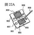
901:外殼901: Shell
902:外殼902: Shell
903:顯示部903: Display part
904:顯示部904: Display part
905:麥克風905: Microphone
906:揚聲器906: Speaker
907:操作鍵907: Operation keys
908:觸控筆908: Stylus
911:外殼911: Shell
912:外殼912: Shell
913:顯示部913: Display Department
914:顯示部914: Display Department
915:連接部915: Connector
916:操作鍵916: Operation keys
921:外殼921: Shell
922:顯示部922: Display part
923:鍵盤923: Keyboard
924:指向裝置924: Pointing Device
931:外殼931: Shell
932:冷藏室門932: Refrigerator door
933:冷凍室門933: Freezer Door
941:外殼941: Shell
942:外殼942: Shell
943:顯示部943: Display Department
944:操作鍵944: Operation keys
945:透鏡945: Lens
946:連接部946: Connector
951:車身951: Body
952:車輪952: Wheels
953:儀表板953: Dashboard
954:燈954: Lamp
1189:ROM介面1189: ROM interface
1190:基板1190: Substrate
1191:ALU1191: ALU
1192:ALU控制器1192: ALU Controller
1193:指令解碼器1193: Instruction Decoder
1194:中斷控制器1194: Interrupt Controller
1195:時序控制器1195: Timing Controller
1196:暫存器1196: scratchpad
1197:暫存器控制器1197: Scratchpad Controller
1198:匯流排介面1198: Bus interface
1199:ROM1199:ROM
1200:記憶元件1200: Memory element
1201:電路1201: Circuits
1202:電路1202: Circuits
1203:開關1203: switch
1204:開關1204: switch
1206:邏輯元件1206: Logic element
1207:電容元件1207: Capacitive element
1208:電容元件1208: Capacitive element
1209:電晶體1209: Transistor
1210:電晶體1210: Transistor
1213:電晶體1213: Transistor
1214:電晶體1214: Transistor
1220:電路1220: Circuits
2100:電晶體2100: Transistor
2200:電晶體2200: Transistor
3001:佈線3001: Wiring
3002:佈線3002: Wiring
3003:佈線3003: Wiring
3004:佈線3004: Wiring
3005:佈線3005: Wiring
3200:電晶體3200: Transistor
3300:電晶體3300: Transistor
3400:電容元件3400: Capacitive element
5000:基板5000: Substrate
5001:像素部5001: Pixel Department
5002:掃描線驅動電路5002: Scan line driver circuit
5003:掃描線驅動電路5003: Scan line driver circuit
5004:信號線驅動電路5004: Signal line driver circuit
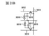
5010:電容線5010: Capacitor Line
5012:掃描線5012: scan line
5013:掃描線5013: scan line
5014:信號線5014: Signal line
5016:電晶體5016: Transistor
5017:電晶體5017: Transistor
5018:液晶元件5018: Liquid Crystal Elements
5019:液晶元件5019: Liquid Crystal Elements
5020:像素5020: Pixel
5021:開關電晶體5021: switching transistor
5022:驅動電晶體5022: drive transistor
5023:電容元件5023: Capacitive element
5024:發光元件5024: Light-emitting element
5025:信號線5025: Signal line
5026:掃描線5026: scan line
5027:電源線5027: Power Cord
5028:共用電極5028: Common electrode
在圖式中:In the schema:
圖1A和圖1B是示出根據本發明的一個實施方式的電晶體的俯視圖及剖面圖;1A and 1B are a top view and a cross-sectional view illustrating a transistor according to an embodiment of the present invention;
圖2A至圖2D是示出根據本發明的一個實施方式的電晶體的一部分的剖面圖;2A-2D are cross-sectional views illustrating a portion of a transistor according to an embodiment of the present invention;
圖3A和圖3B是示出根據本發明的一個實施方式的電晶體的一部分的剖面圖及示出能帶結構的圖;3A and 3B are a cross-sectional view illustrating a portion of a transistor according to an embodiment of the present invention and a diagram illustrating an energy band structure;
圖4A和圖4B是示出根據本發明的一個實施方式的電晶體的剖面圖;4A and 4B are cross-sectional views illustrating a transistor according to an embodiment of the present invention;
圖5A和圖5B是示出根據本發明的一個實施方式的電晶體的製造方法的剖面圖;5A and 5B are cross-sectional views illustrating a method of manufacturing a transistor according to an embodiment of the present invention;
圖6A和圖6B是示出根據本發明的一個實施方式的電晶體的製造方法的剖面圖;6A and 6B are cross-sectional views illustrating a method of manufacturing a transistor according to an embodiment of the present invention;
圖7A和圖7B是示出根據本發明的一個實施方式的電晶體的製造方法的剖面圖;7A and 7B are cross-sectional views illustrating a method of manufacturing a transistor according to an embodiment of the present invention;
圖8A和圖8B是示出根據本發明的一個實施方式的電晶體的製造方法的剖面圖;8A and 8B are cross-sectional views illustrating a method of manufacturing a transistor according to an embodiment of the present invention;
圖9A和圖9B是示出根據本發明的一個實施方式的電晶體的製造方法的俯視圖及剖面圖;9A and 9B are a plan view and a cross-sectional view illustrating a method for manufacturing a transistor according to an embodiment of the present invention;
圖10A和圖10B是示出根據本發明的一個實施方式的電晶體的剖面圖;10A and 10B are cross-sectional views illustrating a transistor according to an embodiment of the present invention;
圖11A和圖11B是示出根據本發明的一個實施方式的電晶體的製造方法的剖面圖;11A and 11B are cross-sectional views illustrating a method of manufacturing a transistor according to an embodiment of the present invention;
圖12A和圖12B是示出根據本發明的一個實施方式的電晶體的製造方法的剖面圖;12A and 12B are cross-sectional views illustrating a method of manufacturing a transistor according to an embodiment of the present invention;
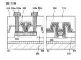
圖13A和圖13B是示出根據本發明的一個實施方式的電晶體的製造方法的剖面圖;13A and 13B are cross-sectional views illustrating a method of manufacturing a transistor according to an embodiment of the present invention;
圖14A和圖14B是示出根據本發明的一個實施方式的半導體裝置的電路圖;14A and 14B are circuit diagrams illustrating a semiconductor device according to an embodiment of the present invention;
圖15是示出根據本發明的一個實施方式的半導體裝置的剖面圖;15 is a cross-sectional view illustrating a semiconductor device according to an embodiment of the present invention;
圖16是示出根據本發明的一個實施方式的半導體裝置的剖面圖;16 is a cross-sectional view illustrating a semiconductor device according to an embodiment of the present invention;
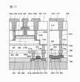
圖17是示出根據本發明的一個實施方式的半導體裝置的剖面圖;17 is a cross-sectional view illustrating a semiconductor device according to an embodiment of the present invention;
圖18A和圖18B是示出根據本發明的一個實施方式的記憶體裝置的電路圖;18A and 18B are circuit diagrams illustrating a memory device according to an embodiment of the present invention;
圖19是示出根據本發明的一個實施方式的CPU的方塊圖;19 is a block diagram illustrating a CPU according to one embodiment of the present invention;
圖20是示出根據本發明的一個實施方式的記憶元件的電路圖;20 is a circuit diagram illustrating a memory element according to an embodiment of the present invention;
圖21A至圖21C是示出根據本發明的一個實施方式的顯示裝置的俯視圖及電路圖;21A to 21C are a top view and a circuit diagram illustrating a display device according to an embodiment of the present invention;
圖22A至圖22F是示出根據本發明的一個實施方式的電子裝置的圖。22A to 22F are diagrams illustrating an electronic device according to an embodiment of the present invention.
下文將參照圖式對本發明的實施方式進行詳細的說明。然而,本發明不侷限於以下說明,所屬技術領域的普通技術人員可以很容易地理解一個事實就是其方式和詳細內容可以被變換為各種形式。此外,本發明不應該被解釋為僅限定在下面的實施方式所記載的內容中。注意,當利用圖式說明發明結構時,表示相同部分的元件符號在不同的圖式中共同使用。另外,在一些情況下使用相同的陰影圖案於相似的部分,而相似的部分不特別附加元件符號表示。Hereinafter, embodiments of the present invention will be described in detail with reference to the drawings. However, the present invention is not limited to the following description, and it can be easily understood by those skilled in the art that the manner and details thereof can be changed into various forms. In addition, this invention should not be construed as being limited only to the content described in the following embodiment. Note that when the invention structure is described using the drawings, the reference numerals denote the same partsNumbers are used together in different schemas. Additionally, in some cases the same hatching pattern is used for similar parts, and similar parts are not specifically designated by reference numerals.
注意,在圖式中,有時為了簡化而誇大尺寸、膜(層)的厚度或區域。Note that in the drawings, dimensions, thicknesses of films (layers), or regions are sometimes exaggerated for simplification.
在本說明書中,例如,為了描述物體形狀,可以將容納物體的最小立方體的一邊長度或者物體的一個剖面的等效圓直徑換稱為物體的“直徑”、“粒徑”、“大小”、“尺寸”、“寬度”。用語「物體的一個剖面的等效圓直徑」是指等於物體的一個剖面具有相同的面積的正圓形的直徑。In this specification, for example, in order to describe the shape of an object, the length of one side of the smallest cube containing the object or the equivalent circle diameter of a section of the object may be referred to as the "diameter", "particle size", "size", "Size", "Width". The term "equivalent circle diameter of one section of an object" refers to the diameter of a perfect circle having the same area as one section of the object.
電壓在大多情況下指某個電位與參考電位(例如,接地電位(GND)或源極電位)之間的電位差。可以將電壓稱為電位而反之亦然。Voltage in most cases refers to the potential difference between a certain potential and a reference potential (eg, a ground potential (GND) or a source potential). Voltage can be called potential and vice versa.
為方便起見,在本說明書中使用第一、第二等序數詞,而其並不表示步驟順序或疊層順序。因此,例如可以將用語“第一”適當地替換為用語“第二”或“第三”等。此外,在本說明書等中記載的序數詞與用於規範本發明的一個實施方式的序數詞不一定一致。For convenience, ordinal numbers such as first and second are used in this specification, and they do not indicate the order of steps or the order of stacking. Thus, for example, the term "first" may be replaced by the term "second" or "third" etc. as appropriate. In addition, the ordinal numbers described in this specification etc. do not necessarily correspond to the ordinal numbers for specifying an embodiment of the present invention.
注意,例如在導電性充分低時,在一些情況下“半導體”包括“絕緣體”的特性。此外,“半導體”和“絕緣體”的邊界不清楚,因此在一些情況下不能精確地區別“半導體”和“絕緣體”。由此,在一些情況下可以將本說明書所記載的“半導體”換稱為“絕緣體”。同樣地,在一些情況下可以將本說明書所記載的“絕緣體”換稱為“半導體”。Note that "semiconductor" includes properties of "insulator" in some cases, such as when the conductivity is sufficiently low. Furthermore, the boundary between "semiconductor" and "insulator" is not clear, so that "semiconductor" and "insulator" cannot be precisely distinguished in some cases. Therefore, the "semiconductor" described in this specification may be referred to as an "insulator" in some cases. Likewise, in someIn this case, the "insulator" described in this specification may be referred to as a "semiconductor".
另外,例如在導電性充分高時,在一些情況下即便表示為“半導體”也具有“導電體”的特性。此外,“半導體”和“導電體”的邊界不清楚,因此在一些情況下不能精確地區別。由此,在一些情況下可以將本說明書所記載的“半導體”換稱為“導電體”。同樣地,在一些情況下可以將本說明書所記載的“導電體”換稱為“半導體”。In addition, for example, when the conductivity is sufficiently high, in some cases, even if it is expressed as a "semiconductor", it has the characteristics of a "conductor". Furthermore, the boundary between "semiconductor" and "conductor" is not clear, and therefore cannot be precisely distinguished in some cases. Therefore, the "semiconductor" described in the present specification may be referred to as a "conductor" in some cases. Similarly, the "conductor" described in this specification may be referred to as a "semiconductor" in some cases.
注意,半導體的雜質例如是指構成半導體的主要成分之外的元素。例如,具有濃度低於0.1atomic%的元素是雜質。當包含雜質時,可在半導體中形成DOS(Density of State:態密度),例如載子移動率可降低或結晶性可降低等。在半導體是氧化物半導體的情況下,改變半導體特性的雜質的例子包括第一族元素、第二族元素、第十四族元素、第十五族元素或主要成分之外的過渡金屬等,具體是,例如有氫(包括水)、鋰、鈉、矽、硼、磷、碳、氮等。在氧化物半導體的情況下,藉由氫等雜質的進入可形成氧缺陷。此外,在半導體是矽膜的情況下,改變半導體特性的雜質的例子包括氧、除氫之外的第一族元素、第二族元素、第十三族元素、第十五族元素等。Note that the impurities of the semiconductor refer to, for example, elements other than the main components constituting the semiconductor. For example, an element having a concentration lower than 0.1 atomic% is an impurity. When an impurity is contained, DOS (Density of State) can be formed in the semiconductor, for example, carrier mobility can be reduced or crystallinity can be reduced. In the case where the semiconductor is an oxide semiconductor, examples of impurities that change the characteristics of the semiconductor include Group 1 elements, Group 2 elements, Group 14 elements, Group 15 elements, or transition metals other than the main components, and the like, specifically Yes, such as hydrogen (including water), lithium, sodium, silicon, boron, phosphorus, carbon, nitrogen, etc. In the case of an oxide semiconductor, oxygen vacancies can be formed by the entry of impurities such as hydrogen. Further, in the case where the semiconductor is a silicon film, examples of impurities that change the characteristics of the semiconductor include oxygen, Group 1 elements other than hydrogen, Group 2 elements, Group 13 elements, Group 15 elements, and the like.
另外,在本說明書中,“A具有濃度B的區域”之記載包括例如:A的某區域中在深度方向上整體區域的濃度為B的情況、A的某區域中在深度方向上的濃度的平均值為B的情況、A的某區域中在深度方向上的濃度的中間值為B的情況、A的某區域中在深度方向上的濃度的最大值為B的情況、A的某區域中在深度方向上的濃度的最小值為B的情況、A的某區域中在深度方向上的濃度的收斂值為B的情況、以及A的某區域中在測量中得到可能的值的濃度為B的情況等。In addition, in this specification, the description of "A region having a concentration B" includes, for example, a case where the concentration of the entire region in the depth direction in a certain region of A is B, and the concentration in a certain region of A in the depth direction. When the average value is B, the concentration in the depth direction in a certain area of AThe case where the median value of the concentration is B, the case where the maximum value of the concentration in the depth direction in a certain region of A is B, the case where the minimum value of the concentration in the depth direction in a certain region of A is B, and the certain region in A A case where the convergence value of the density in the depth direction is B, and a case where the density at which a possible value is obtained during measurement in a certain region of A is B, and the like.
在本說明書中,在記載為“A具有大小B、長度B、厚度B、寬度B或距離B的區域”時,例如包括:A的某區域整體區域的大小、長度、厚度、寬度或距離為B的情況;A的某區域的大小、長度、厚度、寬度或距離的平均值為B的情況;A的某區域的大小、長度、厚度、寬度或距離的中值為B的情況;A的某區域的大小、長度、厚度、寬度或距離的最大值為B的情況;A的某區域的大小、長度、厚度、寬度或距離的最小值為B的情況;A的某區域的大小、長度、厚度、寬度或距離的收斂值為B的情況;以及A的某區域中的在測量中能夠得到可能是個準確的值的大小、長度、厚度、寬度或距離為B的情況等。In this specification, when it is stated that "A has a region of size B, length B, thickness B, width B or distance B", for example, it includes: the size, length, thickness, width or distance of the entire region of A is The case of B; the case where the average value of the size, length, thickness, width or distance of an area of A is B; the case where the median of the size, length, thickness, width or distance of an area of A is B; the case of A's The case where the maximum value of the size, length, thickness, width or distance of a certain area is B; the case where the minimum value of the size, length, thickness, width or distance of a certain area of A is B; the size, length of a certain area of A , where the convergent value of thickness, width, or distance is B; and the size, length, thickness, width, or distance in a certain area of A where the size, length, thickness, width, or distance can be obtained as an accurate value during measurement is B, etc.
注意,例如,通道長度是指在電晶體的俯視圖中,半導體(或在電晶體處於開啟狀態時,在半導體中電流流動的部分)與閘極電極相互重疊的區域或形成有通道的區域中的源極(源極區域或源極電極)與汲極(汲極區域或汲極電極)之間的距離。在一個電晶體中,通道長度不一定在所有的區域中成為相同的值。即,一個電晶體的通道長度在一些情況下不侷限於一個值。因此,在本說明書中,通道長度是形成通道的區域中的任一個值、最大值、最小值或平均值。Note that, for example, the channel length refers to the area where the semiconductor (or the portion where current flows in the semiconductor when the transistor is on) and the gate electrode overlap each other or the area where the channel is formed in the top view of the transistor. The distance between the source (source region or source electrode) and the drain (drain region or drain electrode). In a transistor, the channel length does not necessarily have the same value in all regions. That is, the channel length of one transistor is not limited to one value in some cases. Therefore, in this specification, the channel length is any value in the area where the channel is formed, the maximumvalue, minimum value, or average value.
例如,通道寬度是指半導體(或在電晶體處於開啟狀態時,在半導體中電流流動的部分)與閘極電極相互重疊的區域或形成有通道的區域中的源極與汲極相對的部分的長度。在一個電晶體中,通道寬度在所有區域中不一定為相同。換言之,一個電晶體的通道寬度在一些情況下不侷限於一個值。因此,在本說明書中,通道寬度是形成有通道的區域中的任一個值、最大值、最小值或平均值。For example, the channel width refers to the area where the semiconductor (or the portion of the semiconductor where current flows when the transistor is on) and the gate electrode overlap each other or the portion where the source and drain are opposite in the area where the channel is formed. length. In a transistor, the channel width is not necessarily the same in all regions. In other words, the channel width of a transistor is not limited to one value in some cases. Therefore, in this specification, the channel width is any one value, a maximum value, a minimum value or an average value in the region in which the channel is formed.
另外,取決於電晶體的結構,在一些情況下實際上形成有通道的區域中的通道寬度(下面稱為有效的通道寬度)不同於電晶體的俯視圖所示的通道寬度(下面稱為外觀上的通道寬度)。例如,在具有三維結構的電晶體中,在一些情況下因為有效的通道寬度大於電晶體的俯視圖所示的外觀上的通道寬度,所以不能忽略其影響。例如,在具有微型且三維結構的電晶體中,在一些情況下形成在半導體側面的通道區域的比例大於形成在半導體頂面的通道區域的比例。在此情況下,實際上形成有通道的有效的通道寬度大於俯視圖所示的外觀上的通道寬度。In addition, depending on the structure of the transistor, the channel width in the region where the channel is actually formed (hereinafter referred to as the effective channel width) differs from the channel width shown in the top view of the transistor (hereinafter referred to as the apparent channel width) in some cases channel width). For example, in a transistor having a three-dimensional structure, since the effective channel width is larger than the apparent channel width shown in the top view of the transistor, its influence cannot be ignored in some cases. For example, in transistors having a microscopic and three-dimensional structure, the proportion of channel regions formed on the sides of the semiconductor is in some cases greater than the proportion of channel regions formed on the top surface of the semiconductor. In this case, the effective channel width in which the channel is actually formed is larger than the apparent channel width shown in the plan view.
在具有三維結構的電晶體中,在一些情況下難以藉由實測來估計有效的通道寬度。例如,為了從設計值估計有效的通道寬度,需要假設已知半導體的形狀作為一個假設條件。因此,在半導體的形狀不正確地已知的情況下,難以正確地測定有效的通道寬度。In transistors having a three-dimensional structure, it is difficult in some cases to estimate the effective channel width by actual measurement. For example, in order to estimate the effective channel width from the design value, the shape of the known semiconductor needs to be assumed as an assumption. Therefore, when the shape of the semiconductor is not accurately known, it is difficult to accurately measure the effective channel width.
於是,在本說明書中,在一些情況下在電晶體的俯視圖中將作為半導體與閘極電極相互重疊的區域中的源極與汲極相對的部分的長度的外觀上的通道寬度稱為“圍繞通道寬度(SCW:Surrounded Channel Width)”。此外,在本說明書中,在簡單地表示用語“通道寬度”時,在一些情況下是指圍繞通道寬度或外觀上的通道寬度。或者,在本說明書中,在簡單地表示用語“通道寬度”的情況下,可表示有效的通道寬度。注意,藉由取得剖面TEM影像等並對該影像進行分析等,可以決定通道長度、通道寬度、有效的通道寬度、外觀上的通道寬度、圍繞通道寬度等的值。Therefore, in this specification, the apparent channel width, which is the length of the portion where the source electrode and the drain electrode are opposed to each other in the region where the semiconductor and the gate electrode overlap each other in the top view of the transistor, is referred to as "surrounding" in some cases. Channel width (SCW: Surrounded Channel Width)”. Furthermore, in this specification, when the term "channel width" is simply expressed, it refers to the surrounding channel width or the apparent channel width in some cases. Alternatively, in this specification, where the term "channel width" is simply expressed, the effective channel width may be expressed. Note that the channel length, channel width, effective channel width, apparent channel width, surrounding channel width, etc. can be determined by acquiring a cross-sectional TEM image or the like and analyzing the image.
另外,在藉由計算求得電晶體的場效移動率或每個通道寬度的電流值等的情況下,可使用圍繞通道寬度計算。在此情況下,該求得的值不同於在一些情況下使用有效的通道寬度計算來求得的值。In addition, when the field-effect mobility of the transistor, the current value per channel width, etc. are obtained by calculation, the calculation around the channel width can be used. In this case, the value found differs from the value found using efficient channel width calculations in some cases.
在本說明書中,“A具有其端部比B的端部突出的形狀”可意味著在俯視圖或剖面圖中A的至少一個端部位於B的至少一個端部的外側的情況。因此,例如可以將“A具有其端部比B的端部突出的形狀”的記載解釋為在俯視圖中A的一個端部位於B的一個端部的外側。In this specification, "A has a shape in which the end portion protrudes from the end portion of B" may mean that at least one end portion of A is located outside at least one end portion of B in a plan view or a cross-sectional view. Therefore, for example, the description that "A has a shape in which the end portion protrudes from the end portion of B" can be interpreted as that one end portion of A is located outside the one end portion of B in a plan view.
在本說明書中,“平行”是指兩條直線形成的角度為-10°以上且10°以下的狀態。因此,還包括該角度為-5°以上且5°以下的狀態。另外,“垂直”是指兩條直線形成的角度為80°以上且100°以下的狀態。因此,還包括該角度為85°以上且95°以下的狀態。In this specification, "parallel" refers to a state where the angle formed by two straight lines is -10° or more and 10° or less. Therefore, the state where this angle is -5° or more and 5° or less is also included. In addition, "perpendicular" refers to a state in which the angle formed by two straight lines is 80° or more and 100° or less. Therefore, also includeThis angle is a state of 85° or more and 95° or less.
在本說明書中,六方晶系包括三方晶系和菱方晶系。In this specification, the hexagonal crystal system includes the trigonal crystal system and the rhombohedral crystal system.
〈電晶體的結構〉<Structure of Transistor>
下面,將說明根據本發明的一個實施方式的電晶體的結構。Next, the structure of a transistor according to an embodiment of the present invention will be described.
〈電晶體結構1〉<Transistor structure 1>
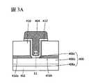
圖1A及圖1B是根據本發明的一個實施方式的電晶體490的俯視圖及剖面圖。圖1A是俯視圖。圖1B是對應於圖1A所示的點劃線A1-A2及點劃線A3-A4的剖面圖。注意,在圖1A的俯視圖中,為了明確起見,省略構成要素的一部分。1A and 1B are a top view and a cross-sectional view of a
在圖1B中,電晶體490包括:基板400上的絕緣體401、絕緣體401上的絕緣體402、絕緣體402上的半導體406、具有與半導體406的頂面及側面接觸的區域的導電體416a及導電體416b、與導電體416a及導電體416b的頂面接觸且具有到達導電體416a的開口部及到達導電體416b的開口部的絕緣體410、藉由絕緣體410的開口部與導電體416a接觸的導電體424a、藉由絕緣體410的開口部與導電體416b接觸的導電體424b、與半導體406的頂面接觸的絕緣體412、隔著絕緣體412配置於半導體406上的導電體404、以及絕緣體410及導電體404上的絕緣體408。In FIG. 1B,
注意,電晶體490不一定包括絕緣體401。電晶體490不一定包括絕緣體402。電晶體490在一些情況下可以不包括絕緣體408。電晶體490不一定包括導電體424a。電晶體490不一定包括導電體424b。Note that
在圖1B中,包括到達導電體424a的開口部及到達導電體424b的開口部的絕緣體418和藉由絕緣體418的開口部分別與導電體424a與導電體424b接觸的導電體426a以及導電體426b位於電晶體490的絕緣體408上。In FIG. 1B , the
在電晶體490中,導電體404作為閘極電極。另外,絕緣體412作為閘極絕緣體。導電體416a及導電體416b作為源極電極以及汲極電極。因此,能夠由施加到導電體404的電位控制半導體406的電阻。即,能夠由施加到導電體404的電位控制導電體416a與導電體416b之間的導通或非導通。In the
另外,電晶體490的導電體404包括隔著絕緣體410與導電體416a重疊的區域以及隔著絕緣體410與導電體416b重疊的區域。電晶體490藉由在導電體404與導電體416a之間及導電體404與導電體416b之間分別包括絕緣體410,藉此可以減小寄生電容。因此,電晶體490高具有頻率特性。In addition, the
如圖1B所示,半導體406的側面與導電體416a及導電體416b接觸。另外,可以由作為閘極電極的導電體404的電場電圍繞半導體406。將由閘極電極的電場電圍繞半導體的電晶體結構稱為surrounded channel(s-channel)結構。因此,在一些情況下通道形成在整個半導體406(bulk)中。在s-channel結構中,可以使大電流流過電晶體的源極與汲極之間,由此可以增大導通時的電流(通態電流)。另外,由於半導體406由導電體404的電場圍繞,所以能夠減少非導通時的電流(關態電流(off-state current))。As shown in FIG. 1B , the side surfaces of the
注意,藉由使電晶體490被具有阻擋氫等雜質及氧的功能的絕緣體圍繞,能夠使電晶體490的電特性穩定。例如,作為絕緣體401及絕緣體408,可以使用具有阻擋氫等雜質及氧的功能的絕緣體。Note that the electrical characteristics of the
作為具有阻擋氫等雜質及氧的功能的絕緣體,例如可以使用包含硼、碳、氮、氧、氟、鎂、鋁、矽、磷、氯、氬、鎵、鍺、釔、鋯、鑭、釹、鉿或鉭的絕緣體的單層或疊層。As an insulator having a function of blocking impurities such as hydrogen and oxygen, for example, boron, carbon, nitrogen, oxygen, fluorine, magnesium, aluminum, silicon, phosphorus, chlorine, argon, gallium, germanium, yttrium, zirconium, lanthanum, and neodymium can be used. , hafnium or tantalum insulators in a single layer or as a stack.
例如,絕緣體401可以由氧化鋁、氧化鎂、氮氧化矽、氮化矽、氧化鎵、氧化鍺、氧化釔、氧化鋯、氧化鑭、氧化釹、氧化鉿或氧化鉭形成。注意,絕緣體401較佳為包含氧化鋁或氮化矽。例如,藉由使絕緣體401包含氧化鋁或氮化矽,能夠抑制氫等雜質混入半導體406。另外,例如,藉由使絕緣體401包含氧化鋁或氮化矽,能夠減少氧向外的擴散。For example, the
另外,例如,絕緣體408可以由氧化鋁、氧化鎂、氮氧化矽、氮化矽、氧化鎵、氧化鍺、氧化釔、氧化鋯、氧化鑭、氧化釹、氧化鉿或氧化鉭形成。注意,絕緣體408較佳為包含氧化鋁或氮化矽。例如,藉由使絕緣體408包含氧化鋁或氮化矽,能夠抑制氫等雜質混入半導體406。另外,例如,藉由使絕緣體408包含氧化鋁或氮化矽,能夠減少氧向外的擴散。Additionally, for example, the
絕緣體402具有例如包含硼、碳、氮、氧、氟、鎂、鋁、矽、磷、氯、氬、鎵、鍺、釔、鋯、鑭、釹、鉿或鉭的絕緣體的單層或疊層。例如,作為絕緣體402,可以由氧化鋁、氧化鎂、氧化矽、氧氮化矽、氮氧化矽、氮化矽、氧化鎵、氧化鍺、氧化釔、氧化鋯、氧化鑭、氧化釹、氧化鉿或氧化鉭形成。
絕緣體402也可以具有防止雜質從基板400擴散的功能。另外,當半導體406為氧化物半導體時,絕緣體402可以具有向半導體406供應氧的功能。The
導電體416a及導電體416b各可以具有例如包含硼、氮、氧、氟、矽、磷、鋁、鈦、鉻、錳、鈷、鎳、銅、鋅、鎵、釔、鋯、鉬、釕、銀、銦、錫、鉭和鎢中的一種以上的導電體的單層或疊層。例如,也可以使用合金或化合物,可以使用包含鋁的導電體、包含銅及鈦的導電體、包含銅及錳的導電體、包含銦、錫及氧的導電體或者包含鈦及氮的導電體等。Each of the
注意,可以取決於導電體416a及導電體416b的端部形狀形成偏置區域和重疊區域。Note that the offset region and the overlapping region may be formed depending on the shape of the end portions of the
在圖2A及圖2B所示的剖面圖中,在導電體416a的端部處半導體406的頂面與導電體416a的側面所形成的角度為θa,在導電體416b的端部處半導體406的頂面與導電體416b的側面所形成的角度為θb。注意,在導電體416a的端部或導電體416b的端部處θa或θb的角度具有範圍時,θa或θb為該角度的平均值、中值、最小值或最大值。In the cross-sectional views shown in FIGS. 2A and 2B , the angle formed by the top surface of the
在圖2A中,θa的角度大且導電體416a的突出量比絕緣體412的厚度小,藉此形成偏置區域Loffa。類似地,在圖2A中,θb的角度大且導電體416b的突出量比絕緣體412的厚度小,藉此形成偏置區域Loffb。例如,θa為60°以上且低於90°即可。另外,例如,θb為60°以上且低於90°即可。注意,Loffa與Loffb的大小可以相同,也可以不同。例如,當Loffa與Loffb的大小相同時,能夠降低半導體裝置中的多個電晶體490的電特性或形狀的偏差。相反的,當Loffa與Loffb的大小不同時,在一些情況下能夠降低由於電場集中在特定區域中而導致的電晶體490的劣化。In FIG. 2A , the angle of θa is large and the protruding amount of the
另一方面,在圖2B中,因為θa的角度小且導電體416a的突出量比絕緣體412的厚度大,所以形成重疊區域Lova。同樣地,在圖2B中,因為θb的角度小且導電體416b的突出量比絕緣體412的厚度大,所以形成重疊區域Lovb。例如,θa為15°以上且低於60°,或為20°以上且低於50°即可。另外,例如,θb為15°以上且低於60°,或為20°以上且低於50°即可。注意,Lova與Lovb的大小可以相同,也可以不同。例如,藉由使Lova與Lovb的大小相同,能夠降低半導體裝置中的多個電晶體490的電特性或形狀的偏差。另外,藉由使Lova與Lovb的大小不同,在一些情況下能夠降低由於電場集中在特定區域中而導致的電晶體490的劣化。On the other hand, in FIG. 2B , since the angle of θa is small and the protruding amount of the
注意,電晶體490也可以包括偏置區域和重疊區域的兩者。例如,藉由具有Lova和Loffb,在一些情況下能夠增大通態電流,並降低由於電場集中在特性區域中而導致的電晶體490的劣化。Note that
在圖2C所示的剖面圖中,在導電體416a的端部處半導體406的頂面與導電體416a的側面所形成的角度大致垂直,在導電體416b的端部處半導體406的頂面與導電體416b的側面所形成的角度大致垂直。此時,絕緣體412的厚度與偏置區域的長度(在圖2C中表示為Loffa及Loffb)相同。In the cross-sectional view shown in FIG. 2C, the angle formed by the top surface of the
在圖2D所示的剖面圖中,導電體416a的端部具有曲面,導電體416b的端部具有曲面。藉由使導電體416a及導電體416b的端部具有曲面,在一些情況下能夠緩和導電體416a及導電體416b的端部處的電場集中。因此,在一些情況下能夠降低由於發生電場集中而導致的電晶體490的劣化。In the cross-sectional view shown in FIG. 2D , the end portion of the
絕緣體410可以具有例如包含硼、碳、氮、氧、氟、鎂、鋁、矽、磷、氯、氬、鎵、鍺、釔、鋯、鑭、釹、鉿或鉭的絕緣體的單層或疊層。例如,絕緣體410可以由氧化鋁、氧化鎂、氧化矽、氧氮化矽、氮氧化矽、氮化矽、氧化鎵、氧化鍺、氧化釔、氧化鋯、氧化鑭、氧化釹、氧化鉿或氧化鉭形成。The
注意,絕緣體410較佳為包括相對介電常數低的絕緣體。例如,絕緣體410較佳為包含氧化矽、氧氮化矽、氮氧化矽、氮化矽或樹脂等。或者,絕緣體410較佳為包括氧化矽或氧氮化矽與樹脂的疊層結構。因為氧化矽及氧氮化矽對熱穩定,所以藉由與樹脂組合,可以實現熱穩定且相對介電常數低的疊層結構。作為樹脂,例如可以舉出聚酯、聚烯烴、聚醯胺(尼龍、芳族聚醯胺等)、聚醯亞胺、聚碳酸酯或丙烯酸等。Note that the
絕緣體412可以具有例如包含硼、碳、氮、氧、氟、鎂、鋁、矽、磷、氯、氬、鎵、鍺、釔、鋯、鑭、釹、鉿或鉭的絕緣體的單層或疊層。例如,絕緣體412可以由氧化鋁、氧化鎂、氧化矽、氧氮化矽、氮氧化矽、氮化矽、氧化鎵、氧化鍺、氧化釔、氧化鋯、氧化鑭、氧化釹、氧化鉿或氧化鉭形成。
注意,絕緣體412較佳為包括相對介電常數高的絕緣體。例如,絕緣體412較佳為包含氧化鎵、氧化鉿、含有鋁及鉿的氧化物、含有鋁及鉿的氧氮化物、含有矽及鉿的氧化物或者含有矽及鉿的氧氮化物等。或者,絕緣體412較佳為包括氧化矽或氧氮化矽與相對介電常數高的絕緣體的疊層結構。因為氧化矽及氧氮化矽對熱穩定,所以藉由與相對介電常數高的絕緣體組合,可以實現熱穩定且相對介電常數高的疊層結構。例如,藉由使絕緣體412的半導體406一側包含氧化鋁、氧化鎵或氧化鉿,能夠抑制氧化矽或氧氮化矽所含有的矽混入半導體406。另外,例如在絕緣體412的半導體406一側包含氧化矽或氧氮化矽時,在一些情況下在氧化鋁、氧化鎵或氧化鉿與氧化矽或氧氮化矽的介面處形成陷阱中心。該陷阱中心在一些情況下可以藉由俘獲電子而使電晶體的臨界電壓向正方向漂移。Note that the
導電體404可以具有例如包含硼、氮、氧、氟、矽、磷、鋁、鈦、鉻、錳、鈷、鎳、銅、鋅、鎵、釔、鋯、鉬、釕、銀、銦、錫、鉭和鎢中的一種以上的導電體的單層或疊層。例如,也可以使用合金或化合物,可以使用包含鋁的導電體、包含銅及鈦的導電體、包含銅及錳的導電體、包含銦、錫及氧的導電體或者包含鈦及氮的導電體等。
導電體424a及導電體424b可以具有例如包含硼、氮、氧、氟、矽、磷、鋁、鈦、鉻、錳、鈷、鎳、銅、鋅、鎵、釔、鋯、鉬、釕、銀、銦、錫、鉭和鎢中的一種以上的導電體的單層或疊層。例如,也可以使用合金或化合物,可以使用包含鋁的導電體、包含銅及鈦的導電體、包含銅及錳的導電體、包含銦、錫及氧的導電體或者包含鈦及氮的導電體等。The
導電體426a及導電體426b可以具有例如包含硼、氮、氧、氟、矽、磷、鋁、鈦、鉻、錳、鈷、鎳、銅、鋅、鎵、釔、鋯、鉬、釕、銀、銦、錫、鉭和鎢中的一種以上的導電體的單層或疊層。例如,也可以使用合金或化合物,可以使用包含鋁的導電體、包含銅及鈦的導電體、包含銅及錳的導電體、包含銦、錫及氧的導電體或者包含鈦及氮的導電體等。
絕緣體418可以具有例如包含硼、碳、氮、氧、氟、鎂、鋁、矽、磷、氯、氬、鎵、鍺、釔、鋯、鑭、釹、鉿或鉭的絕緣體的單層或疊層。例如,絕緣體418可以使用氧化鋁、氧化鎂、氧化矽、氧氮化矽、氮氧化矽、氮化矽、氧化鎵、氧化鍺、氧化釔、氧化鋯、氧化鑭、氧化釹、氧化鉿或氧化鉭形成。
注意,絕緣體418較佳為包括相對介電常數低的絕緣體。例如,絕緣體418較佳為包含氧化矽、氧氮化矽、氮氧化矽、氮化矽或樹脂等。或者,絕緣體418較佳為具有氧化矽或氧氮化矽與樹脂的疊層結構。因為氧化矽及氧氮化矽對熱穩定,所以藉由與樹脂組合,可以實現熱穩定且相對介電常數低的疊層結構。作為樹脂,例如可以舉出聚酯、聚烯經、聚醯胺(尼龍、芳族聚醯胺等)、聚醯亞胺、聚碳酸酯或丙烯酸樹脂等。Note that
作為半導體406,較佳為使用氧化物半導體。注意,在一些情況下可以使用矽(包含應變矽)、鍺、矽鍺、碳化矽、鎵砷、鋁鎵砷、銦磷、氮化鎵或有機半導體等。As the
下面說明氧化物半導體的結構。Next, the structure of the oxide semiconductor will be described.
氧化物半導體大致分為非單晶氧化物半導體和單晶氧化物半導體。非單晶氧化物半導體包括CAAC-OS(C-Axis Aligned Crystalline Oxide Semiconductor:c軸配向結晶氧化物半導體)、多晶氧化物半導體、微晶氧化物半導體以及非晶氧化物半導體等。Oxide semiconductors are roughly classified into non-single crystal oxide semiconductors and single crystal oxide semiconductors. Non-single crystal oxide semiconductors include CAAC-OS (C-Axis Aligned Crystalline Oxide Semiconductor: c-axis aligned crystalline oxide semiconductor), polycrystalline oxide semiconductors, microcrystalline oxide semiconductors, and amorphous oxide semiconductors.
首先,說明CAAC-OS。First, CAAC-OS will be described.
CAAC-OS是包含呈c軸配向的多個結晶部的氧化物半導體之一。CAAC-OS is one of oxide semiconductors including a plurality of crystal parts in a c-axis alignment.
藉由使用穿透式電子顯微鏡(TEM:Transmission Electron Microscope)觀察CAAC-OS的明視野影像及繞射圖案的複合分析影像(也稱為高解析度TEM影像),來能確認到多個結晶部。另一方面,在高解析度TEM影像中,觀察不到各結晶部之間的明確的邊界,即晶界(grain boundary)。因此,在CAAC-OS中,不容易發生由晶界引起的電子移動率的下降。By observing the bright-field image of CAAC-OS and the composite analysis image of the diffraction pattern (also referred to as high-resolution TEM image) using a transmission electron microscope (TEM: Transmission Electron Microscope), a plurality of crystal parts can be confirmed. . On the other hand, in the high-resolution TEM image, clear boundaries between the respective crystal parts, ie, grain boundaries, are not observed. Therefore, in CAAC-OS, a decrease in electron mobility due to grain boundaries does not easily occur.
當從與樣本面大致平行的方向觀察CAAC-OS的高解析度剖面TEM影像時,可以確認到在結晶部中金屬原子排列為層狀。各金屬原子層具有反映了形成CAAC-OS膜的面(也稱為被形成面)或CAAC-OS的頂面的凸凹的形狀並以平行於CAAC-OS的被形成面或頂面的方式排列。When the high-resolution cross-sectional TEM image of CAAC-OS was observed from a direction substantially parallel to the sample surface, it was confirmed that metal atoms were arranged in layers in the crystal portion. Each metal atomic layer has a shape reflecting the convex and concave shape of the surface on which the CAAC-OS film is formed (also referred to as the surface to be formed) or the top surface of the CAAC-OS, and is arranged parallel to the surface to be formed or the top surface of the CAAC-OS .
另一方面,當從與樣本面大致垂直的方向觀察CAAC-OS的平面的高解析度TEM影像時,可知在結晶部中金屬原子排列為三角形狀或六角形狀。但是,在不同的結晶部之間金屬原子的排列沒有規律性。On the other hand, when the high-resolution TEM image of the plane of CAAC-OS was observed from a direction substantially perpendicular to the sample surface, it was found that theThe metal atoms are arranged in a triangular or hexagonal shape. However, there is no regularity in the arrangement of metal atoms between different crystal parts.
使用X射線繞射(XRD:X-Ray Diffraction)裝置對CAAC-OS進行結構分析。例如,當利用out-of-plane法分析包括InGaZnO4結晶的CAAC-OS時,在繞射角(2θ)為31°附近時常出現峰值。由於該峰值來源於InGaZnO4結晶的(009)面,由此可知CAAC-OS中的結晶具有c軸配向性,並且c軸朝向大致垂直於CAAC-OS的被形成面或頂面的方向。Structural analysis of CAAC-OS was performed using an X-ray diffraction (XRD: X-Ray Diffraction) apparatus. For example, when CAAC-OS including InGaZnO4 crystals is analyzed by the out-of-plane method, a peak often appears around a diffraction angle (2θ) of 31°. Since the peak originates from the (009) plane of the InGaZnO4 crystal, it can be seen that the crystal in CAAC-OS has c-axis orientation, and the c-axis is oriented in a direction substantially perpendicular to the formed surface or top surface of CAAC-OS.
注意,當利用out-of-plane法分析包括InGaZnO4結晶的CAAC-OS時,除了在2θ為31°附近的峰值之外,可在2θ為36°附近觀察到峰值。2θ為36°附近的峰值意味著CAAC-OS的一部分中含有不具有c軸配向的結晶。較佳的是,在CAAC-OS中在2θ為31°附近時出現峰值而在2θ為36°附近時不出現峰值。Note that when CAAC-OS including InGaZnO4 crystals was analyzed by the out-of-plane method, a peak was observed around 36° in 2θ in addition to the peak around 31° in 2θ. A peak near 36° in 2θ means that a part of CAAC-OS contains crystals that do not have c-axis alignment. Preferably, in CAAC-OS, a peak occurs when 2θ is around 31° and no peak occurs when 2θ is around 36°.
CAAC-OS是雜質濃度低的氧化物半導體。雜質是指氫、碳、矽、過渡金屬元素等氧化物半導體的主要成分以外的元素。尤其是,某一種元素如矽等與氧的鍵合力比構成氧化物半導體的金屬元素與氧的鍵合力強,該元素會奪取氧化物半導體中的氧,從而打亂氧化物半導體的原子排列,導致結晶性下降。另外,由於鐵或鎳等的重金屬、氬、二氧化碳等的原子半徑(或分子半徑)大,所以若包含在氧化物半導體內,則會打亂氧化物半導體的原子排列,導致結晶性下降。注意,包含在氧化物半導體中的雜質可作為載子陷阱或載子發生源。CAAC-OS is an oxide semiconductor with a low impurity concentration. Impurities refer to elements other than the main components of oxide semiconductors such as hydrogen, carbon, silicon, and transition metal elements. In particular, a certain element such as silicon has a stronger bonding force with oxygen than the metal element constituting the oxide semiconductor and oxygen, and this element will capture the oxygen in the oxide semiconductor, thereby disrupting the atomic arrangement of the oxide semiconductor. lead to a decrease in crystallinity. In addition, heavy metals such as iron and nickel, argon, carbon dioxide, and the like have large atomic radii (or molecular radii), so when contained in an oxide semiconductor, the atomic arrangement of the oxide semiconductor is disturbed, resulting in a decrease in crystallinity. Note that contained in the oxide semiconductorImpurities can act as carrier traps or carrier generation sources.
此外,CAAC-OS是具有缺陷態低密度的氧化物半導體。例如,氧化物半導體中的氧缺陷作為載子陷阱,或當其中俘獲氫時而作為載子發生源。In addition, CAAC-OS is an oxide semiconductor with a low density of defect states. For example, oxygen vacancies in oxide semiconductors serve as carrier traps, or as carrier generation sources when hydrogen is trapped therein.
將雜質濃度低且缺陷態密度低(氧缺陷量少)的狀態稱為“高純度本質”或“實質上高純度本質”。在高純度本質或實質上高純度本質的氧化物半導體中載子發生源少,所以可以降低載子密度。因此,使用該氧化物半導體的電晶體很少具有負臨界電壓的電特性(也稱為常開啟特性)。在高純度本質或實質上高純度本質的氧化物半導體中載子陷阱少。因此,使用該氧化物半導體的電晶體的電特性變動小,於是成為高可靠性電晶體。此外,被氧化物半導體的載子陷阱俘獲的電荷直到被釋放需要長時間。被俘獲的電荷可像固定電荷那樣動作。因此,使用雜質濃度高且缺陷態密度高的氧化物半導體的電晶體可具有不穩定的電特性。A state in which the impurity concentration is low and the density of defect states is low (the amount of oxygen vacancies is small) is called "high-purity nature" or "substantially high-purity nature". In a high-purity or substantially high-purity oxide semiconductor, there are few sources of carrier generation, so the carrier density can be reduced. Therefore, transistors using this oxide semiconductor rarely have electrical characteristics of negative threshold voltage (also referred to as normally-on characteristics). There are few carrier traps in an oxide semiconductor of high purity or substantially high purity. Therefore, a transistor using this oxide semiconductor has little variation in electrical characteristics, and thus becomes a highly reliable transistor. In addition, it takes a long time until the charges trapped by the carrier traps of the oxide semiconductor are released. Trapped charges can behave like fixed charges. Therefore, a transistor using an oxide semiconductor having a high impurity concentration and a high density of defect states may have unstable electrical characteristics.
此外,在使用CAAC-OS的電晶體中,起因於可見光或紫外光的照射的電特性的變動小。In addition, in the transistor using CAAC-OS, there is little variation in electrical properties due to irradiation with visible light or ultraviolet light.
接下來,說明微晶氧化物半導體。Next, the microcrystalline oxide semiconductor will be described.
在微晶氧化物半導體的高解析度TEM影像中有能夠觀察到結晶部的區域和觀察不到明確的結晶部的區域。在微晶氧化物半導體中含有的結晶部的尺寸大多為1nm以上且100nm以下或1nm以上且10nm以下。尤其是,將具有尺寸為1nm以上且10nm以下或1nm以上且3nm以下的微晶的奈米晶(nc:nanocrystal)的氧化物半導體稱為nc-OS(nanocrystalline Oxide Semiconductor:奈米晶氧化物半導體)。另外,例如在nc-OS的高解析度TEM影像中,在一些情況下不能明確地確認到晶界。In the high-resolution TEM image of the microcrystalline oxide semiconductor, there are regions where crystal parts can be observed and regions where no clear crystal parts are observed. The size of the crystal part contained in the microcrystalline oxide semiconductor is often 1 nm or more and 100 nm or less, or 1 nm or more and 10 nm or less. In particular, will have a size of 1 nm or more and 10 nm or less or 1 nm or more andA microcrystalline nanocrystal (nc: nanocrystal) oxide semiconductor of 3 nm or less is called nc-OS (nanocrystalline Oxide Semiconductor: nanocrystalline oxide semiconductor). In addition, for example, in a high-resolution TEM image of nc-OS, grain boundaries cannot be clearly recognized in some cases.
nc-OS在微小區域(例如是1nm以上且10nm以下的區域,特別是1nm以上且3nm以下的區域)中其原子排列具有週期性。另外,nc-OS在不同的結晶部之間觀察不到晶體配向的規律性。因此,在膜整體上觀察不到配向性。所以,在一些情況下nc-OS在某些分析方法中與非晶氧化物半導體沒有差別。例如,在藉由利用使用其束徑比結晶部大的X射線的XRD裝置的out-of-plane法對nc-OS進行結構分析時,檢測不出表示結晶面的峰值。此外,在對nc-OS進行使用其束徑比結晶部大(例如,50nm以上)的電子射線的電子繞射(也稱為選區電子繞射)時,觀察到類似於光暈圖案的繞射圖案。另一方面,在對nc-OS進行使用其束徑近於或小於結晶部的電子射線的奈米束電子繞射時,觀察到斑點。另外,在nc-OS的奈米束電子繞射圖案中,在一些情況下觀察到如圓圈那樣的(環狀的)亮度高的區域。在nc-OS的奈米束電子繞射圖案中,還在一些情況下觀察到環狀的區域內的多個斑點。The atomic arrangement of nc-OS has periodicity in a minute region (for example, a region of 1 nm or more and 10 nm or less, in particular, a region of 1 nm or more and 3 nm or less). In addition, in nc-OS, the regularity of crystal orientation was not observed between different crystal parts. Therefore, no alignment was observed in the entire film. Therefore, in some cases nc-OS does not differ from amorphous oxide semiconductors in certain analytical methods. For example, when the structure of nc-OS is analyzed by the out-of-plane method using an X-ray XRD apparatus whose beam diameter is larger than that of the crystal portion, no peak representing the crystal plane is detected. In addition, when electron diffraction (also referred to as selected-area electron diffraction) using electron rays whose beam diameter is larger than that of the crystal part (eg, 50 nm or more) is performed on nc-OS, diffraction similar to a halo pattern is observed pattern. On the other hand, when the nc-OS was subjected to nanobeam electron diffraction using electron rays whose beam diameter was close to or smaller than that of the crystal portion, spots were observed. In addition, in the nanobeam electron diffraction pattern of nc-OS, a region with high brightness such as a circle (annular) was observed in some cases. In the nanobeam electron diffraction pattern of nc-OS, multiple spots within a ring-shaped region were also observed in some cases.
nc-OS是其規律性比非晶氧化物半導體高的氧化物半導體。因此,nc-OS的缺陷態密度比非晶氧化物半導體低。但是,nc-OS在不同的結晶部之間觀察不到晶體配向的規律性。所以,nc-OS的缺陷態密度比CAAC-OS高。nc-OS is an oxide semiconductor whose regularity is higher than that of an amorphous oxide semiconductor. Therefore, the defect state density of nc-OS is lower than that of amorphous oxide semiconductors. However, in nc-OS, the regularity of crystal orientation is not observed between different crystal parts. Therefore, the defect density of states of nc-OS is higher than that of CAAC-OS.high.
接著,說明非晶氧化物半導體。Next, the amorphous oxide semiconductor will be described.
非晶氧化物半導體是膜中的原子排列沒有規律且不具有結晶部的氧化物半導體。其一個例子為具有如石英那樣的無定形態的氧化物半導體。The amorphous oxide semiconductor is an oxide semiconductor in which the atomic arrangement in the film is irregular and does not have a crystal part. An example of this is an oxide semiconductor having an amorphous state such as quartz.
在非晶氧化物半導體的高解析度TEM影像中無法發現結晶部。No crystal part can be found in the high-resolution TEM image of the amorphous oxide semiconductor.
在使用XRD裝置藉由out-of-plane法對非晶氧化物半導體進行結構分析時,檢測不到表示結晶面的峰值。在對非晶氧化物半導體進行電子繞射時,觀察到光暈圖案。在對非晶氧化物半導體進行奈米束電子繞射時,觀察不到斑點而觀察到光暈圖案。When the structure of the amorphous oxide semiconductor was analyzed by the out-of-plane method using an XRD apparatus, no peak indicating a crystal plane was detected. When the amorphous oxide semiconductor is subjected to electron diffraction, a halo pattern is observed. When an amorphous oxide semiconductor was subjected to nano-beam electron diffraction, no spots were observed but a halo pattern was observed.
注意,氧化物半導體可具有介於nc-OS與非晶氧化物半導體之間的物性的結構。將具有這樣的結構的氧化物半導體特別稱為(類非晶)amorphous-like氧化物半導體(amorphous-like OS:amorphous-like Oxide Semiconductor)。Note that the oxide semiconductor may have a structure with physical properties intermediate between nc-OS and an amorphous oxide semiconductor. An oxide semiconductor having such a structure is particularly called an (amorphous-like) oxide semiconductor (amorphous-like OS: amorphous-like Oxide Semiconductor).
在amorphous-like OS的高解析度TEM影像中在一些情況下觀察到空洞(void)。另外,在高解析度TEM影像中,有能夠明確地觀察到結晶部的區域和不能觀察到結晶部的區域。在amorphous-like OS中,在一些情況下因為用於TEM觀察的微量電子束而產生晶化,由此觀察到結晶部的生長。另一方面,在良好的nc-OS中,幾乎沒有因為用於TEM觀察的微量電子束而產生的晶化。Voids were observed in some cases in high-resolution TEM images of the amorphous-like OS. In addition, in the high-resolution TEM image, there are regions where crystal parts can be clearly observed and regions where crystal parts cannot be observed. In the amorphous-like OS, crystallization occurs due to a trace electron beam used for TEM observation in some cases, whereby the growth of crystal parts is observed. On the other hand, in a good nc-OS, there is almost no crystal formation due to the trace electron beam used for TEM observation.change.
此外,可以使用高解析度TEM影像測定amorphous-like OS及nc-OS的結晶部大小。例如,InGaZnO4的結晶具有層狀結構,在In-O層間具有兩個Ga-Zn-O層。InGaZnO4結晶的單位晶格具有三個In-O層和六個Ga-Zn-O層這九個層在c軸方向上以層狀層疊的結構。因此,這些相鄰的層間的間隔等於(009)面的晶格表面間隔(也稱為d值),經結晶結構分析得出該值為0.29nm。因此,著眼於高解析度TEM影像的晶格條紋,在晶格條紋的間隔為0.28nm以上且0.30nm以下的區域,每個晶格條紋都對應於InGaZnO4的結晶的a-b面。In addition, the crystallite size of amorphous-like OS and nc-OS can be measured using high-resolution TEM images. For example, the crystal of InGaZnO4 has a layered structure with two Ga-Zn-O layers between the In-O layers. The unit lattice of the InGaZnO4 crystal has a structure in which nine layers of three In-O layers and six Ga-Zn-O layers are stacked in layers in the c-axis direction. Therefore, the spacing between these adjacent layers is equal to the lattice surface spacing of the (009) plane (also referred to as the d value), which is 0.29 nm from crystal structure analysis. Therefore, looking at the lattice fringes of the high-resolution TEM image, each lattice fringe corresponds to the ab plane of the InGaZnO4 crystal in the region where the interval between the lattice fringes is 0.28 nm or more and 0.30 nm or less.
注意,氧化物半導體例如可以是包括非晶氧化物半導體、amorphous-like OS、微晶氧化物半導體和CAAC-OS中的兩種以上的疊層膜。Note that the oxide semiconductor may be, for example, a stacked film including two or more of an amorphous oxide semiconductor, an amorphous-like OS, a microcrystalline oxide semiconductor, and a CAAC-OS.
圖3A是將電晶體490的一部分放大的剖面圖。在圖3A中,半導體406是依次層疊半導體層406a、半導體層406b及半導體層406c的疊層膜。FIG. 3A is an enlarged cross-sectional view of a portion of the
對可用於半導體層406a、半導體層406b及半導體層406c等的半導體進行說明。The semiconductor which can be used for the
半導體層406b例如是包含銦的氧化物半導體。例如,在半導體層406b包含銦時,其載子移動率(電子移動率)得到提高。此外,半導體層406b較佳為包含元素M。元素M較佳是鋁、鎵、釔或錫等。作為可用作元素M的其他元素,有硼、矽、鈦、鐵、鎳、鍺、釔、鋯、鉬、鑭、鈰、釹、鉿、鉭、鎢等。注意,作為元素M也可以組合使用上述多個元素。元素M例如是與氧的鍵能高的元素。元素M例如是與氧的鍵能高於銦的元素。或者,元素M例如是可增大氧化物半導體的能隙的元素。此外,半導體層406b較佳為包含鋅。當氧化物半導體包含鋅時,在一些情況下容易晶化。The
注意,半導體層406b不侷限於包含銦的氧化物半導體。半導體層406b例如也可以是鋅錫氧化物、鎵錫氧化物或氧化鎵等不包含銦且包含鋅、鎵或錫的氧化物半導體等。Note that the
作為半導體層406b,例如使用能隙大的氧化物。半導體層406b的能隙例如是2.5eV以上且4.2eV以下,較佳為2.8eV以上且3.8eV以下,更佳為3eV以上且3.5eV以下。As the
例如,半導體層406a及半導體層406c包括構成半導體層406b的氧之外的元素中的一種以上的元素。因為半導體層406a及半導體層406c分別包括構成半導體層406b的氧之外的元素中的一種以上的元素,所以不容易在半導體層406a與半導體層406b的介面以及半導體層406b與半導體層406c的介面處形成介面能階。For example, the
對半導體層406a、半導體層406b及半導體層406c包含銦的情況進行說明。另外,在半導體層406a是In-M-Zn氧化物的情況下,在In和M的總和為100atomic%時,較佳的是:In低於50atomic%,M為50atomic%以上,更佳的是:In低於25atomic%,M為75atomic%以上。此外,在半導體層406b是In-M-Zn氧化物的情況下,在In和M的總和為100atomic%時,較佳的是:In為25atomic%以上,M低於75atomic%,更佳的是:In為34atomic%以上,M低於66atomic%。此外,在半導體層406c是In-M-Zn氧化物的情況下,在In和M的總和為100atomic%時,較佳的是:In低於50atomic%,M為50atomic%以上,更佳的是:In低於25atomic%,M為75atomic%以上。另外,半導體層406c也可以使用與半導體層406a相同的種類的氧化物。The case where the
作為半導體層406b使用其電子親和力大於半導體層406a及半導體層406c的氧化物。例如,作為半導體層406b使用如下氧化物,該氧化物的電子親和力比半導體層406a及半導體層406c大0.07eV以上且1.3eV以下,較佳為大0.1eV以上且0.7eV以下,更佳為大0.15eV以上且0.4eV以下。注意,電子親和力是真空能階和導帶底之間的能量差。As the
銦鎵氧化物的電子親和力小,其氧阻擋性高。因此,半導體層406c較佳為包含銦鎵氧化物。鎵原子的比率[Ga/(In+Ga)]例如為70%以上,較佳為80%以上,更佳為90%以上。Indium gallium oxide has low electron affinity and high oxygen barrier properties. Therefore, the
注意,半導體層406a或/及半導體層406c也可以是氧化鎵。例如,當將氧化鎵用於半導體層406c時,能夠降低在導電體416a或導電體416b與導電體404之間產生的洩漏電流。即,能夠減少電晶體490的關態電流。Note that the
此時,若施加閘極電壓,通道則形成在半導體層406a、半導體層406b和半導體層406c當中的電子親和力大的半導體層406b中。At this time, when a gate voltage is applied, a channel is formed in the
圖3B示出對應於圖3A所示的點劃線E1-E2的能帶結構。圖3B示出真空能階(記為“vacuum level”)、各層的導帶底的能量(記為“Ec”)以及價帶頂(記為“Ev”)。FIG. 3B shows the energy band structure corresponding to the dashed-dotted line E1-E2 shown in FIG. 3A. Figure 3B shows the vacuum energy level (denoted "vacuum level"), the energy of the bottom of the conduction band (denoted "Ec"), and the top of the valence band (denoted "Ev") of each layer.
在此,在一些情況下在半導體層406a與半導體層406b之間具有半導體層406a和半導體層406b的混合區域。另外,在一些情況下在半導體層406b與半導體層406c之間具有半導體層406b和半導體層406c的混合區域。混合區域的介面態密度較低。因此,在半導體層406a、半導體層406b和半導體層406c的疊層體的能帶結構中,各層之間的介面及介面附近的能量連續地變化(也稱為連續接合)。Here, there is a mixed region of the
此時,電子不在半導體層406a中及半導體層406c中移動,而主要在半導體層406b中移動。因此,藉由降低半導體層406a與半導體層406b的介面處的介面態密度、半導體層406b與半導體層406c的介面處的介面態密度,在半導體層406b中妨礙電子移動的情況得到減少,從而可以提高電晶體490的通態電流。At this time, electrons do not move in the
注意,在電晶體490具有s-channel結構的情況下,通道形成在整個半導體層406b中。因此,半導體層406b具有越大的厚度,通道區域越大。即,半導體層406b越厚,電晶體490的通態電流越大。例如,半導體層406b具有其厚度為20nm以上,較佳為40nm以上,更佳為60nm以上,進一步較佳為100nm以上的區域即可。注意,包括電晶體490的半導體裝置的生產率在一些情況下會下降,因此,例如,半導體層406b具有其厚度為300nm以下,較佳為200nm以下,更佳為150nm以下的區域即可。Note that in the case where
此外,為了提高電晶體490的通態電流,半導體層406c的厚度越小越好。例如,半導體層406c具有其厚度低於10nm,較佳為5nm以下,更佳為3nm以下的區域即可。另一方面,半導體層406c具有阻擋構成相鄰的絕緣體的氧之外的元素(氫、矽等)侵入形成有通道的半導體層406b中的功能。因此,半導體層406c較佳為具有一定程度的厚度。例如,半導體層406c具有其厚度為0.3nm以上,較佳為1nm以上,更佳為2nm以上的區域即可。另外,為了抑制從絕緣體402等釋放的氧向外擴散,半導體層406c較佳為具有阻擋氧的性質。In addition, in order to improve the on-state current of the
此外,為了提高可靠性,較佳的是,半導體層406a的厚度大,並且半導體層406c的厚度小。例如,半導體層406a具有其厚度例如為10nm以上,較佳為20nm以上,更佳為40nm以上,進一步較佳為60nm以上的區域即可。藉由將半導體層406a形成得厚,可以拉開相鄰的絕緣體和半導體層406a的介面與形成有通道的半導體層406b的距離。注意,因為包括電晶體490的半導體裝置的生產率在一些情況下會下降,所以半導體層406a具有其厚度例如為200nm以下,較佳為120nm以下,更佳為80nm以下的區域即可。In addition, in order to improve reliability, it is preferable that the thickness of the
例如,氧化物半導體中的矽在一些情況下成為載子陷阱或載子發生源。因此,半導體層406b的矽濃度越低越好。例如,在半導體層406b與半導體層406a之間具有藉由二次離子質譜分析法(SIMS:Secondary Ion Mass Spectrometry)得到的矽濃度低於1×10¹⁹atoms/cm3,較佳為低於5×1018atoms/cm3,更佳為低於2×1018atoms/cm3的區域。此外,在半導體層406b與半導體層406c之間具有藉由SIMS得到的矽濃度低於1×1019atoms/cm3,較佳為低於5×1018atoms/cm3,更佳為低於2×1018atoms/cm3的區域。For example, silicon in an oxide semiconductor becomes a carrier trap or a carrier generation source in some cases. Therefore, the lower the silicon concentration of the
另外,半導體層406b具有藉由SIMS得到的氫濃度為2×1020atoms/cm3以下,較佳為5×1019atoms/cm3以下,更佳為1×1019atoms/cm3以下,進一步較佳為5×1018atoms/cm3以下的區域。此外,為了降低半導體層406b的氫濃度,較佳為降低半導體層406a及半導體層406c的氫濃度。半導體層406a及半導體層406c具有藉由SIMS得到的氫濃度為2×1020atoms/cm3以下,較佳為5×1019atoms/cm3以下,更佳為1×1019atoms/cm3以下,進一步較佳為5×1018atoms/cm3以下的區域。此外,為了降低半導體層406b的氮濃度,較佳為降低半導體層406a及半導體層406c的氮濃度。另外,半導體層406b具有藉由SIMS得到的氮濃度低於5×1019atoms/cm3,較佳為5×1018atoms/cm3以下,更佳為1×1018atoms/cm3以下,進一步較佳為5×1017atoms/cm3以下的區域。半導體層406a及半導體層406c具有藉由SIMS得到的氮濃度低於5×1019atoms/cm3,較佳為5×1018atoms/cm3以下,更佳為1×1018atoms/cm3以下,進一步較佳為5×1017atoms/cm3以下的區域。In addition, the
注意,當銅混入氧化物半導體時,在一些情況下生成電子陷阱。電子陷阱在一些情況下使電晶體的臨界電壓向正方向漂移。因此,半導體層406b的表面或內部的銅濃度越低越好。例如,半導體層406b較佳為具有銅濃度為1×10¹⁹atoms/cm3以下、5×1018atoms/cm3以下或者1×1018atoms/cm3以下的區域。Note that when copper is mixed into an oxide semiconductor, electron traps are generated in some cases. Electron traps in some cases shift the threshold voltage of the transistor in the positive direction. Therefore, the lower the copper concentration on the surface or the inside of the
上述三層結構是一個例子。例如,也可以採用沒有半導體層406a或半導體層406c的兩層結構。或者,也可以採用在半導體層406a上或下、或者在半導體層406c上或下設置作為半導體層406a、半導體層406b和半導體層406c例示的半導體中的任何一個半導體的四層結構。或者,也可以採用在半導體層406a上、半導體層406a下、半導體層406c上、半導體層406c下中的任何兩個以上的位置設置作為半導體層406a、半導體層406b和半導體層406c例示的半導體中的任何一個半導體的n層結構(n為5以上的整數)。The above three-layer structure is an example. For example, a two-layer structure without the
作為基板400例如可以使用絕緣體基板、半導體基板或導電體基板。作為絕緣體基板,例如可以舉出玻璃基板、石英基板、藍寶石基板、安定氧化鋯基板(釔安定氧化鋯基板等)、樹脂基板等。例如,作為半導體基板,可以舉出由矽或鍺等構成的單一材料的半導體基板、或者由碳化矽、矽鍺、砷化鎵、磷化銦、氧化鋅或氧化鎵等構成的化合物半導體基板等。並且,還可以舉出在上述半導體基板內部具有絕緣體區域的半導體基板,例如為SOI(Silicon On Insulator;絕緣體上覆矽)基板等。作為導電體基板,可以舉出石墨基板、金屬基板、合金基板、導電樹脂基板等。或者,可以舉出包含金屬的氮化物的基板、包含金屬的氧化物的基板等。再者,還可以舉出設置有導電體或半導體的絕緣體基板、設置有導電體或絕緣體的半導體基板、設置有半導體或絕緣體的導電體基板等。或者,也可以使用在這些基板上設置有元件的基板。作為在基板上被設置的元件,可以舉出電容元件、電阻元件、切換元件、發光元件、記憶元件等。As the
此外,作為基板400也可以使用撓性基板。另外,作為在撓性基板上設置電晶體的方法,也可以舉出如下方法:在不具有撓性的基板上形成電晶體之後,剝離電晶體而將該電晶體轉置到撓性基板的基板400上。在此情況下,較佳為在不具有撓性的基板與電晶體之間設置剝離層。此外,作為基板400,也可以使用包含纖維的薄片、薄膜或箔等。另外,基板400也可以具有伸縮性。此外,基板400可以具有在停止彎曲或拉伸時恢復為原來的形狀的性質。或者,也可以具有不恢復為原來的形狀的性質。基板400例如具有其厚度為5μm以上且700μm以下,較佳為10μm以上且500μm以下,更佳為15μm以上且300μm以下的區域。藉由將基板400形成得薄,可以實現包括電晶體490的半導體裝置的輕量化。另外,藉由將基板400形成得薄,即便在使用玻璃等的情況下,基板400也在一些情況下會具有伸縮性或在停止彎曲或拉伸時恢復為原來的形狀的性質。因此,可以緩和因掉落等而基板400上的半導體裝置受到的衝擊等。即,能夠提供一種耐久性高的半導體裝置。In addition, a flexible substrate can also be used as the
撓性基板的基板400例如可以使用金屬、合金、樹脂、玻璃或其纖維等。撓性基板的基板400的線膨脹係數越低,因環境而發生的變形越得到抑制,所以是較佳的。撓性基板的基板400例如使用線膨脹係數為1×10⁻³/K以下、5×10-5/K以下或1×10-5/K以下的材料即可。作為樹脂,例如可以舉出聚酯、聚烯烴、聚醯胺(尼龍、芳族聚醯胺等)、聚醯亞胺、聚碳酸酯、丙烯酸樹脂等。尤其是芳族聚醯胺的線膨脹係數較低,因此撓性基板的基板400較佳為使用芳族聚醯胺。As the
注意,電晶體490也可以採用圖4A或圖4B所示的剖面圖的結構。圖4A與圖1B的不同之處是在絕緣體402下包括導電體413。另外,圖4B與圖4A的不同之處是導電體413與導電體404電連接。Note that the
導電體413作為電晶體490的第二閘極(還稱為背閘極電極)。例如,也可以對導電體413施加低於或高於源極電極的電壓而使電晶體490的臨界電壓在正或負方向上漂移。例如,藉由使電晶體490的臨界電壓向正方向漂移,在一些情況下即便閘極電壓為0V也能夠實現電晶體490成為非導通狀態(關閉狀態)的常關閉(normally-off)。注意,施加到導電體413的電壓既可為可變的,又可為固定的。
導電體413可以具有例如包含硼、氮、氧、氟、矽、磷、鋁、鈦、鉻、錳、鈷、鎳、銅、鋅、鎵、釔、鋯、鉬、釕、銀、銦、錫、鉭和鎢中的一種以上的導電體的單層或疊層。例如,也可以使用合金或化合物,還可以使用包含鋁的導電體、包含銅及鈦的導電體、包含銅及錳的導電體、包含銦、錫及氧的導電體或者包含鈦及氮的導電體等。
〈電晶體結構1的製造方法〉<Manufacturing method of transistor structure 1>
下面,對圖1A和圖1B所示的電晶體490的製造方法進行說明。Next, a method of manufacturing the
首先,準備基板400。First, the
接著,形成絕緣體401。絕緣體401可以藉由濺射法、化學氣相沉積(CVD:Chemical Vapor Deposition)法、分子束磊晶(MBE:Molecular Beam Epitaxy)法、脈衝雷射沉積(PLD:Pulsed Laser Deposition)法、原子層沉積(ALD:Atomic Layer Deposition)法等形成。Next, the
注意,CVD法可以分為利用電漿的電漿CVD(PECVD:Plasma Enhanced CVD)法、利用熱量的熱CVD(TCVD:Thermal CVD)法及利用光的光CVD(Photo CVD)法等。再者,CVD法可以根據使用的源氣體被分為金屬CVD(MCVD:Metal CVD)法及有機金屬CVD(MOCVD:Metal Organic CVD)法。Note that the CVD method can be classified into a plasma CVD (PECVD: Plasma Enhanced CVD) method using plasma, a thermal CVD (TCVD: Thermal CVD) method using heat, and a photo CVD (Photo CVD) method using light. In addition, the CVD method can be classified into a metal CVD (MCVD: Metal CVD) method and an organic metal CVD (MOCVD: Metal Organic CVD) method according to the source gas used.
藉由利用電漿CVD法,可以以較低的溫度得到高品質的膜。另外,因為在熱CVD法中不使用電漿,所以能夠減少對被處理物造成的電漿損傷。例如,包括在半導體裝置中的佈線、電極、元件(電晶體、電容元件等)等在一些情況下因從電漿接收電荷而會產生電荷積聚(charge buildup)。在此情況下,由於所累積的電荷可使包括在半導體裝置中的佈線、電極、元件等受損傷。另一方面,在採用不使用電漿的熱CVD法的情況下,因為這種電漿損傷小,所以能夠提高半導體裝置的良率。另外,在熱CVD法中,成膜時的電漿損傷小,因此能夠得到缺陷較少的膜。By utilizing the plasma CVD method, a high-quality film can be obtained at a relatively low temperature. In addition, since plasma is not used in the thermal CVD method, plasma damage to the object to be processed can be reduced. For example, wirings, electrodes, elements (transistors, capacitive elements, etc.), etc. included in a semiconductor device may generate charge buildup due to receiving electric charges from plasma in some cases. In this case, wirings, electrodes, elements, etc. included in the semiconductor device may be damaged due to the accumulated charges. On the other hand, when the thermal CVD method that does not use plasma is used, since such plasma damage is small, the yield of the semiconductor device can be improved. In addition, in the thermal CVD method, since the plasma damage during film formation is small, a film with few defects can be obtained.
另外,ALD法也是能夠減少對被處理物造成的電漿損傷的成膜方法。此外,ALD法的成膜時的電漿損傷也小,所以能夠得到缺陷較少的膜。In addition, the ALD method is also a film-forming method capable of reducing plasma damage to the object to be processed. In addition, since the plasma damage during film formation by the ALD method is also small, a film with few defects can be obtained.
不同於從靶材等中被釋放的粒子沉積的成膜方法,CVD法及ALD法是因被處理物表面的反應而形成膜的形成方法。因此,藉由CVD法及ALD法形成的膜不易受被處理物的形狀的影響而具有良好的步階覆蓋性。尤其是,藉由ALD法形成的膜具有良好的步階覆蓋性和厚度均勻性,所以ALD法適合用於形成覆蓋縱橫比高的開口部的表面的膜。但是,ALD法的沉積速度比較慢,所以在一些情況下較佳為與沉積速度快的CVD法等其他成膜方法組合而使用。Different from the deposition method of particles released from the target, the CVD method and the ALD method are formed by the reaction of the surface of the object to be processed.Method of forming the film. Therefore, the film formed by the CVD method and the ALD method is not easily affected by the shape of the object to be processed and has good step coverage. In particular, since the film formed by the ALD method has good step coverage and thickness uniformity, the ALD method is suitable for forming a film covering the surface of an opening with a high aspect ratio. However, since the deposition rate of the ALD method is relatively slow, in some cases, it is preferable to use it in combination with other film-forming methods such as the CVD method which has a high deposition rate.
CVD法或ALD法可以藉由調整源氣體的流量比控制所得到的膜的組成。例如,當使用CVD法或ALD法時,可以藉由調整源氣體的流量比形成任意組成的膜。此外,例如,當使用CVD法或ALD法時,可以藉由一邊形成膜一邊改變源氣體的流量比來形成其組成連續變化的膜。在一邊改變源氣體的流量比一邊形成膜時,因為可以省略傳送及調整壓力所需的時間,所以與使用多個成膜室進行成膜的情況相比可以使其成膜時所需的時間縮短。因此,在一些情況下可以提高半導體裝置的生產率。In the CVD method or the ALD method, the composition of the obtained film can be controlled by adjusting the flow ratio of the source gas. For example, when the CVD method or the ALD method is used, a film of any composition can be formed by adjusting the flow rate ratio of the source gas. Further, for example, when the CVD method or the ALD method is used, a film whose composition is continuously changed can be formed by changing the flow rate ratio of the source gas while forming the film. When a film is formed while changing the flow rate ratio of the source gas, the time required for conveying and adjusting the pressure can be omitted, so the time required for film formation can be compared with the case of using a plurality of film forming chambers for film formation shorten. Therefore, the productivity of the semiconductor device can be improved in some cases.
接著,形成絕緣體402(參照圖5A)。絕緣體402可以使用濺射法、CVD法、MBE法、PLD法或ALD法等形成。Next, the
接著,也可以進行對絕緣體402添加氧的處理。作為添加氧的處理,例如有離子植入法、電漿處理法等。另外,對絕緣體402添加的氧成為過剩氧。Next, a process of adding oxygen to the
接著,形成半導體。半導體可以使用濺射法、CVD法、MBE法、PLD法或ALD法等形成。Next, a semiconductor is formed. The semiconductor can be formed using a sputtering method, a CVD method, an MBE method, a PLD method, an ALD method, or the like.
接著,也可以進行對半導體添加氧的處理。作為添加氧的處理,例如有離子植入法、電漿處理法等。注意,對半導體添加的氧成為過剩氧。注意,當半導體為疊層膜時,較佳為對對應於成為圖3A的半導體層406a的半導體的層進行添加氧的處理。Next, a treatment of adding oxygen to the semiconductor may be performed. As the treatment for adding oxygen, there are, for example, an ion implantation method, a plasma treatment method, and the like. Note that the oxygen added to the semiconductor becomes excess oxygen. Note that when the semiconductor is a laminated film, it is preferable to perform a treatment of adding oxygen to the layer corresponding to the semiconductor to be the
接著,較佳為進行第一加熱處理。第一加熱處理以250℃以上且650℃以下的溫度,較佳為以450℃以上且600℃以下的溫度,更佳為以520℃以上且570℃以下的溫度進行即可。第一加熱處理在惰性氣體氛圍或者包含10ppm以上、1%以上或10%以上的氧化性氣體的氛圍下進行。第一加熱處理也可以在減壓狀態下進行。或者,也可以以如下方法進行第一加熱處理:在惰性氣體氛圍下進行加熱處理之後,為了填補脫離了的氧而在包含10ppm以上、1%以上或10%以上的氧化性氣體氛圍下進行另一個加熱處理。藉由進行第一加熱處理,可以提高半導體的結晶性,並可以去除氫或水等雜質。Next, it is preferable to perform the first heat treatment. The first heat treatment may be performed at a temperature of 250°C or higher and 650°C or lower, preferably 450°C or higher and 600°C or lower, more preferably 520°C or higher and 570°C or lower. The first heat treatment is performed in an inert gas atmosphere or an atmosphere containing 10 ppm or more, 1% or more, or 10% or more of an oxidizing gas. The first heat treatment may be performed in a reduced pressure state. Alternatively, the first heat treatment may be performed by a method in which, after the heat treatment in an inert gas atmosphere, another heat treatment is performed in an oxidizing gas atmosphere containing 10 ppm or more, 1% or more, or 10% or more in order to replace the desorbed oxygen. a heat treatment. By performing the first heat treatment, the crystallinity of the semiconductor can be improved, and impurities such as hydrogen and water can be removed.
接著,藉由光微影法等對半導體進行加工形成半導體406(參照圖5B)。注意,當形成半導體406時,在一些情況下絕緣體402的一部分也被蝕刻而變薄。即,絕緣體402可在與半導體406接觸的區域具有凸部。Next, the semiconductor is processed by photolithography or the like to form a semiconductor 406 (see FIG. 5B ). Note that when the
接著,形成導電體。導電體可以使用濺射法、CVD法、MBE法、PLD法或ALD法等形成。Next, a conductor is formed. The conductor can be formed by sputtering, CVD, MBE, PLD, ALD, or the like.
接著,藉由光微影法等對導電體進行加工形成導電體416(參照圖6A)。注意,導電體416覆蓋半導體406。Next, the conductors are processed by photolithography or the like to form conductors 416 (see FIG. 6A ). Note that
在光微影法中,首先藉由光罩對光阻劑進行曝光。接著,使用顯影液去除或留下所曝光的區域而形成光阻遮罩。接著,藉由該光阻遮罩進行蝕刻處理來將導電體、半導體或絕緣體等加工為所希望的形狀。例如,使用KrF準分子雷射、ArF準分子雷射、EUV(Extreme Ultraviolet:極紫外)光等對光阻劑進行曝光來形成光阻遮罩,即可。此外,也可以利用在基板和投影透鏡之間填滿液體(例如,水)的狀態下進行曝光的液浸技術。另外,也可以使用電子束或離子束代替上述光。注意,當使用電子束或離子束時,不需要光罩。另外,可以使用灰化處理等乾蝕刻處理或/及濕蝕刻處理來去除光阻遮罩。In photolithography, the photoresist is first exposed through a photomask. Next, a developer is used to remove or leave the exposed areas to form a photoresist mask. Next, an etching process is performed by this photoresist mask, and a conductor, a semiconductor, an insulator, etc. are processed into a desired shape. For example, the photoresist mask may be formed by exposing the photoresist using KrF excimer laser, ArF excimer laser, EUV (Extreme Ultraviolet) light, or the like. In addition, a liquid immersion technique in which exposure is performed in a state where a liquid (eg, water) is filled between the substrate and the projection lens can also be used. In addition, an electron beam or an ion beam may be used instead of the above-mentioned light. Note that when using an electron beam or ion beam, a reticle is not required. In addition, the photoresist mask may be removed by dry etching treatment such as ashing treatment or/and wet etching treatment.
接著,形成絕緣體438(參照圖6B)。絕緣體438可以使用濺射法、CVD法、MBE法、PLD法或ALD法等形成。另外,絕緣體438可以使用旋塗法、浸漬法、液滴噴射法(噴墨法等)、印刷法(網版印刷、平板印刷等)、刮刀(doctor knife)法、輥塗(roll coater)法或簾式塗布(curtain coater)法等形成。Next, the
絕緣體438以其頂面具有平坦性的方式形成。例如,在成膜剛結束後,絕緣體438的頂面可以具有平坦性。或者,例如,在成膜後,可以從上面去除絕緣體438以使絕緣體438的頂面平行於基板背面等基準面。將這種處理稱為平坦化處理。作為平坦化處理,有化學機械拋光(CMP:Chemical Mechanical Polishing)處理、乾蝕刻處理等。注意,絕緣體438的頂面也可以不具有平坦性。The
接著,藉由光微影法等對絕緣體438進行加工形成絕緣體439,該絕緣體439包括到達將在後面成為導電體416a的區域的開口部及到達將在後面成為導電體416b的區域的開口部。Next, the
接著,形成導電體。導電體可以使用濺射法、CVD法、MBE法、PLD法或ALD法等形成。導電體以填充絕緣體439的開口部的方式形成。因此,較佳為使用CVD法(尤其是MCVD法)。另外,為了提高藉由CVD法成膜的導電體的緊密性,在一些情況下較佳為採用藉由ALD法等成膜的導電體與藉由CVD法成膜的導電體的疊層膜。例如,可以使用依次形成有氮化鈦與鎢的疊層膜等。Next, a conductor is formed. The conductor can be formed by sputtering, CVD, MBE, PLD, ALD, or the like. The conductor is formed so as to fill the opening of the
接著,以平行於基板背面等基準面的方式從上面去除導電體,直到僅在絕緣體439的開口部中留下導電體為止。此時,將從絕緣體439的開口部露出的導電體分別稱為導電體424a及導電體424b(參照圖7A)。Next, the conductor is removed from the upper surface so as to be parallel to the reference plane such as the back surface of the substrate until the conductor remains only in the opening of the
接著,藉由光微影法等對絕緣體439進行加工形成絕緣體410。Next, the
接著,藉由光微影法等對導電體416進行加工形成導電體416a及導電體416b(參照圖7B)。注意,絕緣體439的加工與導電體416的加工可以在同一光微影製程中進行。藉由在同一光微影製程中進行加工,能夠減少製程數。因此,能夠提高包括電晶體490的半導體裝置的生產率。或者,絕緣體439的加工與導電體416的加工可以在不同的光微影製程中進行。藉由在不同的光微影製程中進行加工可容易將各膜形成為不同形狀。Next, the
此時,半導體406成為露出的狀態。At this time, the
接著,形成絕緣體。絕緣體可以使用濺射法、CVD法、MBE法、PLD法或ALD法等形成。在形成於絕緣體410、導電體416a及導電體416b的開口部的側面及底面以均勻的厚度形成絕緣體。因此,較佳為使用ALD法。Next, an insulator is formed. The insulator can be formed using a sputtering method, a CVD method, an MBE method, a PLD method, an ALD method, or the like. The insulators are formed with uniform thicknesses on the side surfaces and bottom surfaces of the openings formed in the
接著,形成導電體。導電體可以使用濺射法、CVD法、MBE法、PLD法或ALD法等形成。導電體以填充形成在絕緣體410等的開口部的方式形成。因此,較佳為使用CVD法(尤其是MCVD法)。另外,為了提高藉由CVD法成膜的導電體的緊密性,在一些情況下較佳為採用藉由ALD法等成膜的導電體與藉由CVD法成膜的導電體的疊層膜。例如,可以使用依次形成有氮化鈦與鎢的疊層膜等。Next, a conductor is formed. The conductor can be formed by sputtering, CVD, MBE, PLD, ALD, or the like. The conductor is formed so as to fill the opening formed in the
接著,藉由光微影法等對導電體進行加工形成導電體404。Next, the conductor is processed by photolithography or the like to form the
接著,藉由光微影法等對絕緣體進行加工形成絕緣體412(參照圖8A)。注意,導電體的加工與絕緣體的加工也可以在同一光微影製程中進行。藉由在同一光微影製程中進行加工,能夠減少製程數。因此,能夠提高包括電晶體490的半導體裝置的生產率。或者,導電體的加工與絕緣體的加工可以在不同的光微影製程中進行。藉由在不同的光微影製程中進行加工,可容易將各膜形成為不同形狀。另外,雖然在此示出對絕緣體進行加工形成絕緣體412的例子,但是根據本發明的一個實施方式的電晶體不侷限於此。例如,絕緣體可以不被加工而直接被用作絕緣體412。Next, the insulator is processed by photolithography or the like to form the insulator 412 (see FIG. 8A ). Note that the processing of the conductors and the processing of the insulators can also be performed in the same photolithography process. By processing in the same photolithography process, the number of processes can be reduced. Therefore, it is possible to improveProductivity of semiconductor
接著,形成成為絕緣體408的絕緣體。成為絕緣體408的絕緣體可以使用濺射法、CVD法、MBE法、PLD法或ALD法等形成。Next, an insulator to be the
在形成成為絕緣體408的絕緣體之後,在任何時候都可以進行第二加熱處理。藉由進行第二加熱處理,由於包含在絕緣體402等中的過剩氧移動到半導體406,因此能夠降低半導體406的缺陷(氧缺陷)。注意,第二加熱處理以絕緣體402中的過剩氧(氧)擴散到半導體406的溫度進行即可。例如,關於第二加熱處理,可以參照第一加熱處理的記載。或者,第二加熱處理較佳為以比第一加熱處理低的溫度進行。第一加熱處理與第二加熱處理的溫度之差例如為20℃以上且150℃以下,較佳為40℃以上且100℃以下。由此,能夠抑制過剩氧(氧)過多地從絕緣體402釋放。注意,當在形成各層時進行的加熱處理可以兼作第二加熱處理時,在一些情況下不一定要進行第二加熱處理。After forming the insulator to become the
接著,形成成為絕緣體418的絕緣體。成為絕緣體418的絕緣體可以使用濺射法、CVD法、MBE法、PLD法或ALD法等形成。Next, an insulator to be the
接著,藉由光微影法等對成為絕緣體418的絕緣體進行加工形成絕緣體418。Next, the
接著,藉由光微影法等對成為絕緣體408的絕緣體進行加工形成絕緣體408。注意,成為絕緣體418的絕緣體的加工與成為絕緣體408的絕緣體的加工可以在同一光微影製程中進行。藉由在同一光微影製程中進行加工,能夠減少製程數。因此,能夠提高包括電晶體490的半導體裝置的生產率。或者,成為絕緣體418的絕緣體的加工與成為絕緣體408的絕緣體的加工可以在不同的光微影製程中進行。藉由在不同的光微影製程中進行加工,可容易將各膜形成為不同形狀。Next, the
此時,導電體424a及導電體424b成為露出的狀態。At this time, the
接著,形成導電體。導電體可以使用濺射法、CVD法、MBE法、PLD法或ALD法等形成。Next, a conductor is formed. The conductor can be formed by sputtering, CVD, MBE, PLD, ALD, or the like.
接著,藉由光微影法等對導電體進行加工形成導電體426a及導電體426b(參照圖8B)。Next, the conductors are processed by photolithography or the like to form
藉由上述步驟,可以製造圖1A和圖1B所示的電晶體490。Through the above steps, the
在電晶體490中,可以根據各層的厚度或形狀等控制偏置區域或重疊區域的尺寸等。因此,可以使偏置區域或重疊區域的尺寸等比光微影法的最小加工尺寸小,所以容易實現電晶體的微型化。另外,寄生電容也小,所以能夠實現頻率特性高的電晶體。In the
〈電晶體結構2〉<Transistor structure 2>
下面,說明具有與圖1A和圖1B等所示的電晶體490不同結構的電晶體590。圖9A及圖9B是根據本發明的一個實施方式的電晶體590的俯視圖及剖面圖。圖9A是俯視圖。圖9B是對應於圖9A所示的點劃線B1-B2及點劃線B3-B4的剖面圖。注意,在圖9A的俯視圖中,為了明確起見,省略構成要素的一部分。Next, a
在圖9B中,電晶體590包括:基板500上的絕緣體501、絕緣體501上的絕緣體502、絕緣體502上的半導體506、具有與半導體506的頂面接觸的區域的導電體516a及導電體516b、與導電體516a及導電體516b的頂面接觸的絕緣體510、與半導體506的頂面接觸的絕緣體512、隔著絕緣體512配置於半導體506上的導電體504、以及絕緣體510及導電體504上的絕緣體508。In FIG. 9B,
注意,電晶體590在一些情況下不一定包括絕緣體501。電晶體590在一些情況下不一定包括絕緣體502。電晶體590在一些情況下不一定包括絕緣體508。Note that
在圖9B中,絕緣體518在電晶體590的絕緣體508上。絕緣體518、絕緣體508及絕緣體510具有到達導電體516a的開口部和到達導電體516b的開口部。另外,電晶體590包括分別藉由絕緣體518、絕緣體508及絕緣體510中的開口部與導電體516a與導電體516b接觸的導電體524a和導電體524b、與導電體524a接觸的導電體526a、以及與導電體524b接觸的導電體526b。In FIG. 9B ,
在電晶體590中,導電體504作為閘極電極。另外,絕緣體512作為閘極絕緣體。另外,導電體516a及導電體516b作為源極電極以及汲極電極。因此,能夠由施加到導電體504的電位控制半導體506的電阻。即,能夠由施加到導電體504的電位控制導電體516a與導電體516b之間的導通/非導通。In the
在電晶體590中,導電體504包括隔著絕緣體510與導電體516a重疊的區域以及隔著絕緣體510與導電體516b重疊的區域。電晶體590包括絕緣體510在導電體504與導電體516a之間及導電體504與導電體516b之間,藉此減小寄生電容。因此,電晶體590具有高頻率特性的電晶體。In the
如圖9B所示,可以由導電體504的電場電圍繞半導體506。即,電晶體590具有s-channel結構。因此,能夠增大電晶體的通態電流。另外,能夠減少電晶體的關態電流。另外,由於導電體516a及導電體516b不接觸於半導體506的側面,所以由導電體504的電場圍繞半導體506的效果被強化。因此,電晶體590比電晶體490更容易得到s-channel結構的益處。As shown in FIG. 9B , the
注意,藉由使電晶體590被具有阻擋氫等雜質及氧的功能的絕緣體圍繞時,能夠使電晶體590的電特性穩定。例如,作為絕緣體501及絕緣體508,可以使用具有阻擋氫等雜質及氧的功能的絕緣體。Note that when the
注意,關於基板500,參照基板400的記載。關於絕緣體501,參照絕緣體401的記載。關於絕緣體502,參照絕緣體402的記載。關於半導體506,參照半導體406的記載。關於導電體516a,參照導電體416a的記載。關於導電體516b,參照導電體416b的記載。關於絕緣體512,參照絕緣體412的記載。關於導電體504,參照導電體404的記載。關於絕緣體508,參照絕緣體408的記載。關於絕緣體518,參照絕緣體418的記載。關於導電體524a,參照導電體424a的記載。關於導電體524b,參照導電體424b的記載。關於導電體526a,參照導電體426a的記載。另外,關於導電體526b,參照導電體426b的記載。Note that, regarding the
注意,電晶體590也可以具有圖10A或圖10B所示的剖面圖的結構。圖10A與圖9B的不同之處是在絕緣體502下包括導電體513。另外,圖10B與圖10A的不同之處是導電體513與導電體504電連接。Note that the
導電體513作為電晶體590的第二閘極電極(還稱為背閘極電極)。例如,也可以對導電體513施加低於或高於源極電極的電壓而使電晶體590的臨界電壓在正或負方向上漂移。例如,藉由使電晶體590的臨界電壓向正方向漂移,在一些情況下即便閘極電壓為0V也能夠實現電晶體590成為非導通狀態(關閉狀態)的常關閉。注意,施加到導電體513的電壓既可為可變的,又可為固定的。The
注意,關於導電體513,參照導電體413的記載。Note that regarding the
〈電晶體結構2的製造方法〉<Manufacturing method of transistor structure 2>
下面,對圖9A和圖9B所示的電晶體590的製造方法進行說明。Next, a method of manufacturing the
首先,準備基板500。First, the
接著,形成絕緣體501。絕緣體501可以使用濺射法、CVD法、MBE法、PLD法或ALD法等形成。Next, the
接著,形成絕緣體502(參照圖11A)。絕緣體502可以使用濺射法、CVD法、MBE法、PLD法或ALD法等形成。Next, an
接著,也可以進行對絕緣體502添加氧的處理。作為添加氧的處理,例如有離子植入法、電漿處理法等。另外,對絕緣體502添加的氧成為過剩氧。Next, a process of adding oxygen to the
接著,形成半導體。半導體可以使用濺射法、CVD法、MBE法、PLD法或ALD法等形成。Next, a semiconductor is formed. The semiconductor can be formed using a sputtering method, a CVD method, an MBE method, a PLD method, an ALD method, or the like.
接著,也可以進行對半導體添加氧的處理。作為添加氧的處理,例如有離子植入法、電漿處理法等。注意,對半導體添加的氧成為過剩氧。注意,當半導體為疊層膜時,較佳為對對應於成為圖3A的半導體層406a的半導體的層進行添加氧的處理。Next, a treatment of adding oxygen to the semiconductor may be performed. As the treatment for adding oxygen, there are, for example, an ion implantation method, a plasma treatment method, and the like. Note that the oxygen added to the semiconductor becomes excess oxygen. Note that when the semiconductor is a laminated film, it is preferable to perform a treatment of adding oxygen to the layer corresponding to the semiconductor to be the
接著,較佳為進行第一加熱處理。第一加熱處理以250℃以上且650℃以下的溫度,較佳為以450℃以上且600℃以下的溫度,更佳為以520℃以上且570℃以下的溫度進行即可。第一加熱處理在惰性氣體氛圍或者包含10ppm以上、1%以上或10%以上的氧化性氣體的氛圍下進行。第一加熱處理也可以在減壓狀態下進行。或者,也可以以如下方法進行第一加熱處理:在惰性氣體氛圍下進行加熱處理之後,為了填補脫離了的氧而在包含10ppm以上、1%以上或10%以上的氧化性氣體氛圍下進行另一個加熱處理。藉由進行第一加熱處理,例如可以提高半導體的結晶性,並可以去除氫或水等雜質。Next, it is preferable to perform the first heat treatment. The first heat treatment may be performed at a temperature of 250°C or higher and 650°C or lower, preferably 450°C or higher and 600°C or lower, more preferably 520°C or higher and 570°C or lower. The first heat treatment is performed in an inert gas atmosphere or an atmosphere containing 10 ppm or more, 1% or more, or 10% or more of an oxidizing gas. The first heat treatment may be performed in a reduced pressure state. Alternatively, the first heat treatment may be performed by a method in which, after the heat treatment in an inert gas atmosphere, another heat treatment is performed in an oxidizing gas atmosphere containing 10 ppm or more, 1% or more, or 10% or more in order to replace the desorbed oxygen. a heat treatment. By performing the first heat treatment, for example, the crystallinity of the semiconductor can be improved, and impurities such as hydrogen and water can be removed.
接著,形成導電體。導電體可以使用濺射法、CVD法、MBE法、PLD法或ALD法等形成。Next, a conductor is formed. The conductor can be formed by sputtering, CVD, MBE, PLD, ALD, or the like.
接著,藉由光微影法等對導電體進行加工形成導電體516。Next, the conductor is processed by photolithography or the like to form the
接著,透過導電體516對半導體進行蝕刻,使形成半導體506(參照圖11B)。注意,當形成半導體506時,在一些情況下絕緣體502的一部分也被蝕刻而變薄。即,絕緣體502在與半導體506接觸的區域中可具有凸部。Next, the semiconductor is etched through the
接著,形成絕緣體538(參照圖12A)。絕緣體538可以使用濺射法、CVD法、MBE法、PLD法或ALD法等形成。另外,絕緣體538可以使用旋塗法、浸漬法、液滴噴射法(噴墨法等)、印刷法(網版印刷、平板印刷等)、刮刀(doctor knife)法、輥塗(roll coater)法或簾式塗布(curtain coater)法等形成。Next, an
絕緣體538的頂面也可以具有平坦性。The top surface of the
接著,藉由光微影法等對絕緣體538進行加工形成絕緣體539。Next, the
接著,藉由光微影法等對導電體516進行加工形成導電體516a及導電體516b(參照圖12B)。注意,絕緣體538的加工與導電體516的加工也可以在同一光微影製程中進行。藉由在同一光微影製程中進行加工,能夠減少製程數。因此,能夠提高包括電晶體590的半導體裝置的生產率。或者,絕緣體538的加工與導電體516的加工可以在不同的光微影製程中進行。藉由在不同的光微影製程中進行加工,可容易將各膜形成為不同形狀。Next, the
此時,半導體506成為露出的狀態。At this time, the
接著,形成絕緣體。絕緣體可以使用濺射法、CVD法、MBE法、PLD法或ALD法等形成。在形成於絕緣體539、導電體516a及導電體516b的開口部的側面及底面以均勻的厚度形成絕緣體。因此,較佳為使用ALD法。Next, an insulator is formed. The insulator can be formed using a sputtering method, a CVD method, an MBE method, a PLD method, an ALD method, or the like. The insulators are formed with uniform thicknesses on the side surfaces and the bottom surfaces of the openings formed in the
接著,形成導電體。導電體可以使用濺射法、CVD法、MBE法、PLD法或ALD法等形成。導電體以填充形成在絕緣體539等的開口部的方式形成。因此,較佳為使用CVD法(尤其是MCVD法)。另外,為了提高藉由CVD法成膜的導電體的緊密性,在一些情況下較佳為採用藉由ALD法等成膜的導電體與藉由CVD法成膜的導電體的疊層膜。例如,可以使用依次形成有氮化鈦與鎢的疊層膜等。Next, a conductor is formed. The conductor can be formed by sputtering, CVD, MBE, PLD, ALD, or the like. The conductor is formed so as to fill the opening formed in the
接著,藉由光微影法等對導電體進行加工形成導電體504。Next, the conductors are processed by photolithography or the like to form
接著,藉由光微影法等對絕緣體進行加工形成絕緣體512(參照圖13A)。注意,導電體的加工與絕緣體的加工也可以在同一光微影製程中進行。藉由在同一光微影製程中進行加工,能夠減少製程數。因此,能夠提高包括電晶體590的半導體裝置的生產率。或者,導電體的加工與絕緣體的加工可以在不同的光微影製程中進行。藉由在不同的光微影製程中進行加工,可容易將各膜形成為不同形狀。另外,雖然在此示出對絕緣體進行加工形成絕緣體512的例子,但是根據本發明的一個實施方式的電晶體不侷限於此。例如,絕緣體在一些情況下可以不被加工而直接被用作絕緣體512。Next, the insulator is processed by photolithography or the like to form the insulator 512 (see FIG. 13A ). Note that the processing of the conductors and the processing of the insulators can also be performed in the same photolithography process. By processing in the same photolithography process, the number of processes can be reduced. Therefore, the productivity of the semiconductor device including the
接著,形成成為絕緣體508的絕緣體。成為絕緣體508的絕緣體可以使用濺射法、CVD法、MBE法、PLD法或ALD法等形成。Next, an insulator to be the
在形成成為絕緣體508的絕緣體之後,在任何時候都可以進行第二加熱處理。藉由進行第二加熱處理,由於包含在絕緣體502等中的過剩氧移動到半導體506,因此能夠降低半導體506的缺陷(氧缺陷)。注意,第二加熱處理以絕緣體502中的過剩氧(氧)擴散到半導體506的溫度進行即可。例如,關於第二加熱處理,可以參照第一加熱處理的記載。或者,第二加熱處理較佳為以比第一加熱處理低的溫度進行。第一加熱處理與第二加熱處理的溫度之差例如為20℃以上且150℃以下,較佳為40℃以上且100℃以下。由此,能夠抑制過剩氧(氧)過多地從絕緣體502釋放。注意,當在形成各層時進行的加熱處理可以兼作第二加熱處理時,不一定需要進行第二加熱處理。After forming the insulator to become the
接著,形成成為絕緣體518的絕緣體。成為絕緣體518的絕緣體可以使用濺射法、CVD法、MBE法、PLD法或ALD法等形成。Next, an insulator to be the
接著,藉由光微影法等對成為絕緣體518的絕緣體進行加工形成絕緣體518。Next, the
接著,藉由光微影法等對成為絕緣體508的絕緣體進行加工形成絕緣體508。注意,成為絕緣體518的絕緣體的加工與成為絕緣體508的絕緣體的加工可以在同一光微影製程中進行。藉由在同一光微影製程中進行加工,能夠減少製程數。因此,能夠提高包括電晶體590的半導體裝置的生產率。或者,成為絕緣體518的絕緣體的加工與成為絕緣體508的絕緣體的加工可以在不同的光微影製程中進行。藉由在不同的光微影製程中進行加工,可容易將各膜形成為不同形狀。Next, the
接著,藉由光微影法等對絕緣體539進行加工形成絕緣體510。注意,成為絕緣體518的絕緣體的加工、成為絕緣體508的絕緣體的加工與絕緣體539的加工可以在同一光微影製程中進行。藉由在同一光微影製程中進行加工,能夠減少製程數。因此,能夠提高包括電晶體590的半導體裝置的生產率。或者,成為絕緣體518的絕緣體的加工、成為絕緣體508的絕緣體的加工與絕緣體539的加工可以在不同的光微影製程中進行。藉由在不同的光微影製程中進行加工,可容易將各膜形成為不同形狀。Next, the
此時,導電體516a及導電體516b成為露出的狀態。At this time, the
接著,形成導電體。導電體可以使用濺射法、CVD法、MBE法、PLD法或ALD法等形成。導電體以填充絕緣體518、絕緣體508及絕緣體510的開口部的方式形成。因此,較佳為使用CVD法(尤其是MCVD法)。另外,為了提高藉由CVD法成膜的導電體的緊密性,在一些情況下較佳為採用藉由ALD法等成膜的導電體與藉由CVD法成膜的導電體的疊層膜。例如,可以使用依次形成有氮化鈦與鎢的疊層膜等。Next, a conductor is formed. The conductor can be formed by sputtering, CVD, MBE, PLD, ALD, or the like. The conductor is formed so as to fill the openings of the
接著,以平行於基板背面等基準面的方式從上面去除導電體,直到僅在絕緣體518、絕緣體508及絕緣體510的開口部中留下導電體為止。此時,將從絕緣體518、絕緣體508及絕緣體510的開口部露出的導電體分別稱為導電體524a及導電體524b。Next, the conductors are removed from the upper surface so as to be parallel to the reference plane such as the back surface of the substrate until only the conductors remain in the openings of the
接著,形成導電體。導電體可以使用濺射法、CVD法、MBE法、PLD法或ALD法等形成。Next, a conductor is formed. Electrical conductors can be sputteredmethod, CVD method, MBE method, PLD method or ALD method.
接著,藉由光微影法等對導電體進行加工形成導電體526a及導電體526b(參照圖13B)。Next, the conductors are processed by photolithography or the like to form
藉由上述步驟,可以製造圖9A和圖9B所示的電晶體590。Through the above steps, the
在電晶體590中,可以根據各層的厚度或形狀等控制偏置區域或重疊區域的尺寸等。因此,可以使偏置區域或重疊區域的大小等比光微影法的最小加工尺寸小,所以容易實現電晶體的微型化。另外,寄生電容也小,所以能夠實現頻率特性高的電晶體。In the
〈半導體裝置〉<Semiconductor device>
下面,例示出根據本發明的一個實施方式的半導體裝置。Hereinafter, a semiconductor device according to an embodiment of the present invention will be exemplified.
〈電路〉<circuit>
下面,說明利用根據本發明的一個實施方式的電晶體的電路的一個例子。Next, an example of a circuit using a transistor according to an embodiment of the present invention will be described.
[CMOS反相器][CMOS inverter]
圖14A所示的電路圖示出所謂的CMOS反相器的結構,其中使p通道型電晶體2200與n通道型電晶體2100串聯連接,並使各閘極連接。The circuit diagram shown in FIG. 14A shows the structure of a so-called CMOS inverter in which a p-
〈半導體裝置的結構〉<Structure of Semiconductor Device>
圖15是對應於圖14A的半導體裝置的剖面圖。圖15所示的半導體裝置包括電晶體2200以及配置於電晶體2200的上方的電晶體2100。注意,雖然這裡示出作為電晶體2100使用圖1A和圖1B所示的電晶體490的例子,但是根據本發明的一個實施方式的半導體裝置不侷限於此。例如,作為電晶體2100也可以使用圖4A或圖4B所示的電晶體490、圖9A和圖9B所示的電晶體590、圖10A或圖10B所示的電晶體590等。因此,關於電晶體2100,適當地參照上述電晶體的記載。FIG. 15 is a cross-sectional view of the semiconductor device corresponding to FIG. 14A . The semiconductor device shown in FIG. 15 includes a
圖15所示的電晶體2200是使用半導體基板450的電晶體。電晶體2200包括半導體基板450中的區域474a、半導體基板450中的區域474b、半導體基板450中的區域470、絕緣體462以及導電體454。注意,電晶體2200在一些情況下可以不包括區域470。The
在電晶體2200中,區域474a及區域474b具有源極區域及汲極區域的功能。另外,區域470具有控制臨界電壓的功能。另外,絕緣體462具有閘極絕緣體的功能。另外,導電體454具有閘極電極的功能。因此,能夠由施加到導電體454的電位控制通道形成區域的電阻。即,能夠由施加到導電體454的電位控制區域474a與區域474b間的導通或非導通。In the
作為半導體基板450,例如可以使用由矽或鍺等構成的單一材料的半導體基板、或者由碳化矽、矽鍺、砷化鎵、磷化銦、氧化鋅或氧化鎵等構成的化合物半導體基板等。較佳的是,作為半導體基板450使用單晶矽基板。As the
作為半導體基板450使用包含賦予n型導電性的雜質的半導體基板。注意,作為半導體基板450,也可以使用包含賦予p型導電性的雜質的半導體基板。此時,在成為電晶體2200的區域中配置包含賦予n型導電性的雜質的井,即可。或者,半導體基板450也可以為i型。As the
半導體基板450的頂面較佳為具有(110)面。由此,能夠提高電晶體2200的導通特性。The top surface of the
區域474a及區域474b是包含賦予p型導電性的雜質的區域。由此,電晶體2200具有p通道型的結構。The
區域470是其賦予n型導電性的雜質濃度高於半導體基板450或井的區域。即,藉由包括區域470,能夠使電晶體2200的臨界電壓向負方向漂移。因此,即便在將功函數高的導電體用於導電體454的情況下也容易得到常關閉的電特性。由於在很多情況下功函數高的導電體的耐熱性比功函數低的導電體高,因此後面製程的彈性可得到提高,從而能夠提高半導體裝置的性能。The
注意,電晶體2200與鄰接的電晶體被區域460等隔開。區域460具有絕緣性。Note that
圖15所示的半導體裝置包括絕緣體464、絕緣體466、絕緣體468、導電體480a、導電體480b、導電體480c、導電體478a、導電體478b、導電體478c、導電體476a、導電體476b、導電體416c、導電體424c以及導電體426c。The semiconductor device shown in FIG. 15 includes an
將絕緣體464配置於電晶體2200上。另外,將絕緣體466配置於絕緣體464上。另外,將絕緣體468配置於絕緣體466上。另外,將電晶體2100及導電體416c配置於絕緣體468上。The
絕緣體464包括到達區域474a的開口部、到達區域474b的開口部以及到達導電體454的開口部。另外,導電體480a、導電體480b或導電體480c分別埋入在各開口部中。The
另外,絕緣體466包括到達導電體480a的開口部、到達導電體480b的開口部以及到達導電體480c的開口部。另外,導電體478a、導電體478b或導電體478c分別埋入在各開口部中。In addition, the
另外,絕緣體468包括到達導電體478b的開口部以及到達導電體478c的開口部。另外,導電體476a或導電體476b分別埋入在各開口部中。In addition, the
導電體476a與電晶體2100的導電體416b接觸。另外,導電體476b與導電體416c接觸。
絕緣體410包括到達導電體416c的開口部。另外,導電體424c埋入在開口部中。The
絕緣體418及絕緣體408包括到達導電體424c的開口部以及到達導電體404的開口部。另外,導電體424c與導電體404藉由各開口部由導電體426c電連接。
注意,圖16所示的半導體裝置與圖15所示的半導體裝置的不同之處只在於電晶體2200的結構。因此,關於圖16所示的半導體裝置,參照圖15所示的半導體裝置的記載。明確而言,在圖16所示的半導體裝置中,電晶體2200為Fin型。藉由使電晶體2200成為Fin型,有效的通道寬度得到增大,從而能夠提高電晶體2200的導通特性。另外,由於可以增大閘極電極的電場影響,所以能夠提高電晶體2200的關閉特性。Note that the semiconductor device shown in FIG. 16 is different from the semiconductor device shown in FIG. 15 only in the structure of the
另外,圖17所示的半導體裝置與圖15所示的半導體裝置的不同之處只在於電晶體2200的結構。因此,關於圖17所示的半導體裝置,參照圖15所示的半導體裝置的記載。明確而言,在圖17所示的半導體裝置中,電晶體2200使用SOI基板形成。圖17示出區域456與半導體基板450被絕緣體452隔開的結構。藉由使用SOI基板,可以降低穿通電流等,所以能夠提高電晶體2200的關閉特性。注意,絕緣體452可以藉由使半導體基板450的一部分絕緣體化形成。例如,作為絕緣體452可以使用氧化矽。In addition, the semiconductor device shown in FIG. 17 is different from the semiconductor device shown in FIG. 15 only in the structure of the
在圖15、圖16及圖17所示的半導體裝置中,由於使用半導體基板形成p通道型電晶體,並在其上方製造n通道型電晶體,因此能夠減少元件所占的面積。即,可以提高半導體裝置的集成度。另外,與使用同一半導體基板形成n通道型電晶體與p通道型電晶體的情況相比,可以簡化製程,所以能夠提高半導體裝置的生產率。另外,能夠提高半導體裝置的良率。另外,p通道型電晶體在一些情況下可以省略LDD(Lightly Doped Drain)區域的形成、淺溝槽(Shallow Trench)結構的形成或彎曲設計等複雜的製程。因此,與使用半導體基板形成n通道型電晶體的半導體裝置相比,圖15至圖17所示的半導體裝置在一些情況下能夠提高生產率和良率。In the semiconductor devices shown in FIGS. 15 , 16 , and 17 , since the p-channel transistor is formed using the semiconductor substrate and the n-channel transistor is fabricated on the semiconductor substrate, the area occupied by the element can be reduced.That is, the integration degree of the semiconductor device can be improved. In addition, compared with the case where the n-channel type transistor and the p-channel type transistor are formed using the same semiconductor substrate, the manufacturing process can be simplified, so that the productivity of the semiconductor device can be improved. In addition, the yield of the semiconductor device can be improved. In addition, the p-channel transistor can omit complicated processes such as the formation of an LDD (Lightly Doped Drain) region, the formation of a shallow trench (Shallow Trench) structure, or a curved design in some cases. Therefore, the semiconductor devices shown in FIGS. 15 to 17 can improve productivity and yield in some cases, compared to semiconductor devices in which n-channel type transistors are formed using a semiconductor substrate.
[CMOS類比開關][CMOS analog switch]
此外,圖14B所示的電路圖示出使電晶體2100和電晶體2200的各源極和汲極連接的結構。藉由採用這種結構,可以將該電晶體用作所謂的CMOS類比開關。In addition, the circuit diagram shown in FIG. 14B shows a structure in which the respective sources and drains of the
[記憶體裝置的例子][Example of memory device]
參照圖18A和圖18B示出半導體裝置(記憶體裝置)的一個例子,其中使用根據本發明的一個實施方式的電晶體,即便在沒有電力供應的情況下也能夠保持儲存內容,並且對寫入次數也沒有限制。Referring to FIGS. 18A and 18B , there is shown an example of a semiconductor device (memory device) in which a transistor according to an embodiment of the present invention is used, the stored content can be maintained even in the absence of power supply, and the write There is no limit to the number of times.
圖18A所示的半導體裝置包括使用第一半導體的電晶體3200、使用第二半導體的電晶體3300以及電容元件3400。另外,作為電晶體3300可以使用上述電晶體。The semiconductor device shown in FIG. 18A includes a
電晶體3300是使用氧化物半導體的電晶體。由於電晶體3300的關態電流小,所以可以長期間在半導體裝置的特定的節點中保持儲存內容。即,因為不需要更新工作或可以使更新工作的頻率極低,所以能夠實現低功耗的半導體裝置。The
在圖18A中,第一佈線3001與電晶體3200的源極電連接,第二佈線3002與電晶體3200的汲極電連接。此外,第三佈線3003電連接於電晶體3300的源極和汲極中的一個,第四佈線3004與電晶體3300的閘極電連接。再者,電晶體3200的閘極及電晶體3300的源極和汲極中的另一個電連接於電容元件3400的一個電極,第五佈線3005與電容元件3400的另一個電極電連接。In FIG. 18A , the
圖18A所示的半導體裝置藉由具有能夠保持電晶體3200的閘極的電位的特徵,可以如下所示進行資訊的寫入、保持以及讀出。Since the semiconductor device shown in FIG. 18A has the feature of being able to hold the potential of the gate of the
對資訊的寫入及保持進行說明。首先,將第四佈線3004的電位設定為使電晶體3300成為導通狀態的電位,而使電晶體3300處於導通狀態。由此,第三佈線3003的電位被施加到與電晶體3200的閘極及電容元件3400的一個電極電連接的節點FG。換言之,對電晶體3200的閘極施加規定的電荷(寫入)。這裡,施加賦予兩種不同電位位準的電荷(以下,稱為低位準電荷、高位準電荷)中的任一個。然後,將第四佈線3004的電位設定為使電晶體3300成為非導通狀態的電位而使電晶體3300處於非導通狀態。由此,在節點FG中保持電荷(保持)。The writing and holding of information will be described. First, the potential of the
因為電晶體3300的關態電流極小,所以節點FG的電荷被長時間保持。Since the off-state current of the
接著,對資訊的讀出進行說明。當在對第一佈線3001施加規定的電位(恆電位)的狀態下對第五佈線3005施加適當的電位(讀出電位)時,第二佈線3002具有對應於保持在節點FG中的電荷量的電位。這是因為:在電晶體3200為n通道型電晶體的情況下,對電晶體3200的閘極施加高位準電荷時的外觀上的臨界電壓Vth_H低於對電晶體3200的閘極施加低位準電荷時的外觀上的臨界電壓Vth_L。在此,外觀上的臨界電壓是指為了使電晶體3200成為導通狀態所需要的第五佈線3005的電位。由此,藉由將第五佈線3005的電位設定為Vth_H與Vth_L之間的電位V0,可以辨別施加到節點FG的電荷。例如,在寫入時節點FG被供應高位準電荷的情況下,若第五佈線3005的電位為V0(>Vth_H),電晶體3200則成為“導通狀態”。另一方面,當節點FG被供應低位準電荷時,即便第五佈線3005的電位為V0(<Vth_L),電晶體3200還保持“非導通狀態”。因此,藉由辨別第二佈線3002的電位,可以讀出節點FG所保持的資訊。Next, the reading of information will be described. When an appropriate potential (readout potential) is applied to the
注意,當將記憶單元設置為陣列狀時,在讀出時必須讀出所希望的記憶單元的資訊。為了不讀出其他記憶單元的資訊,對第五佈線3005施加不管施加到節點FG的電荷如何都使電晶體3200成為“非導通狀態”的電位,即低於Vth_H的電位。或者,對第五佈線3005施加不管施加到節點FG的電荷如何都使電晶體3200成為“導通狀態”的電位,即高於Vth_L的電位。Note that when the memory cells are arranged in an array, the information of the desired memory cell must be read out when reading. In order not to read information of other memory cells, the
圖18B所示的半導體裝置與圖18A所示的半導體裝置不同之處是圖18B所示的半導體裝置不包括電晶體3200。在此情況下也可以藉由與圖18A所示的半導體裝置相同的工作進行資訊的寫入及保持工作。The semiconductor device shown in FIG. 18B is different from the semiconductor device shown in FIG. 18A in that the semiconductor device shown in FIG. 18B does not include the
下面,說明圖18B所示的半導體裝置中的資訊讀出。在電晶體3300成為導通狀態時,使處於浮動狀態的第三佈線3003和電容元件3400為導通,且在第三佈線3003和電容元件3400之間再次分配電荷。其結果,使第三佈線3003的電位產生變化。第三佈線3003的電位的變化量根據電容元件3400的一個電極的電位(或積累在電容元件3400中的電荷)而具有不同的值。Next, information readout in the semiconductor device shown in FIG. 18B will be described. When the
例如,在再次分配電荷之後的第三佈線3003的電位為(CB×VB0+C×V)/(CB+C),其中電容元件3400的一個電極的電位為V,電容元件3400的電容為C,第三佈線3003的電容成分為CB,在再次分配電荷之前的第三佈線3003的電位為VB0時。因此可發現,假設記憶單元處於電容元件3400的一個電極的電位為V1和V0(V1>V0)的兩種狀態之任一種狀態中時,可知保持電位V1(=(CB×VB0+C×V1)/(CB+C))的電容元件3400的一個電極的情況下第三佈線3003的電位高於保持電位V0(=(CB×VB0+C×V0)/(CB+C))的電容元件3400的一個電極的情況下第三佈線3003的電位。For example, the potential of the
並且,藉由對第三佈線3003的電位和規定的電位進行比較可以讀出資訊。Then, information can be read out by comparing the potential of the
在此情況下,可以採用一種結構,其中將上述應用第一半導體的電晶體用於用來驅動記憶單元的驅動電路,且在驅動電路上作為電晶體3300層疊應用第二半導體的電晶體。In this case, a structure may be adopted in which the above-described transistor using the first semiconductor is used for the drive circuit for driving the memory cell, and the transistor using the second semiconductor is stacked as the
上述半導體裝置可以應用使用氧化物半導體的關態電流極小的電晶體來長期間保持儲存內容。即,因為不需要更新工作或可以使更新工作的頻率極低,所以能夠實現低功耗的半導體裝置。此外,在沒有電力的供應時(但較佳為固定電位)也可以長期間保持儲存內容。The above-described semiconductor device can maintain storage contents for a long period of time by applying a transistor using an oxide semiconductor with an extremely small off-state current. That is, since the refresh operation is not required or the frequency of the refresh operation can be made extremely low, a semiconductor device with low power consumption can be realized. In addition, the stored content can be maintained for a long period of time even when there is no power supply (but preferably a fixed potential).
此外,因為該半導體裝置在寫入資訊時不需要高電壓,所以其中不容易產生元件的劣化。例如,不同於習知的非揮發性記憶體,不需要對浮動閘極注入電子或從浮動閘極抽出電子,因此不會發生絕緣體劣化等問題。換言之,在根據本發明的一個實施方式的半導體裝置中,在現有非揮發性記憶體中成為問題的重寫次數不受到限制,並且其可靠性得到極大提高。再者,根據電晶體的導通狀態或非導通狀態而進行資訊寫入,所以能夠高速工作。In addition, since the semiconductor device does not require a high voltage when writing information, deterioration of elements therein is less likely to occur. For example, unlike conventional non-volatile memories, there is no need to inject electrons into or extract electrons from the floating gate, so problems such as insulator degradation do not occur. In other words, in the semiconductor device according to one embodiment of the present invention, the number of rewrites, which is a problem in the existing non-volatile memory, is not limited, and the reliability thereof is greatly improved. Furthermore, since information writing is performed according to the conduction state or the non-conduction state of the transistor, high-speed operation is possible.
〈CPU〉<CPU>
下面說明包括上述電晶體或上述記憶體裝置等半導體裝置的CPU。Next, a CPU including a semiconductor device such as the above-described transistor or the above-described memory device will be described.
圖19是示出其一部分使用上述電晶體的CPU的一個例子的結構的塊圖。FIG. 19 is a block diagram showing the configuration of an example of a CPU in which a part of the above-described transistors is used.
圖19所示的CPU在基板1190上具有:ALU1191(ALU:Arithmetic logic unit:算術電路)、ALU控制器1192、指令解碼器1193、中斷控制器1194、時序控制器1195、暫存器1196、暫存器控制器1197、匯流排介面1198、能夠重寫的ROM1199以及ROM介面1189。作為基板1190使用半導體基板、SOI基板、玻璃基板等。ROM1199及ROM介面1189也可以設置在不同的晶片上。當然,圖19所示的CPU只是簡化其結構而所示的一個例子而已,所以實際上的CPU根據其用途具有各種各樣的結構。例如,也可以以包括圖19所示的CPU或算術電路的結構為核心,設置多個該核心並使其同時工作。另外,在CPU的內部算術電路或資料匯流排中能夠處理的位元數例如可以為8位元、16位元、32位元、64位元等。The CPU shown in FIG. 19 has on the substrate 1190: an ALU 1191 (ALU: Arithmetic logic unit: arithmetic circuit), an
藉由匯流排介面1198輸入到CPU的指令在輸入到指令解碼器1193並被解碼後輸入到ALU控制器1192、中斷控制器1194、暫存器控制器1197、時序控制器1195。Commands input to the CPU through the
ALU控制器1192、中斷控制器1194、暫存器控制器1197、時序控制器1195根據被解碼的指令進行各種控制。明確而言,ALU控制器1192生成用來控制ALU1191的工作的信號。另外,中斷控制器1194在執行CPU的程式時,根據其優先度或遮罩狀態來判斷來自外部的輸入/輸出裝置或週邊電路的中斷要求而對該要求進行處理。暫存器控制器1197生成暫存器1196的位址,並對應於CPU的狀態來進行暫存器1196的讀出或寫入。The
另外,時序控制器1195生成用來控制ALU1191、ALU控制器1192、指令解碼器1193、中斷控制器1194以及暫存器控制器1197的工作時序的信號。例如,時序控制器1195具有根據基準時脈信號來生成內部時脈信號的內部時脈生成器,並將內部時脈信號供應到上述各種電路。In addition, the
在圖19所示的CPU中,在暫存器1196中設置有記憶單元。作為暫存器1196的記憶單元,可以使用上述電晶體或記憶體裝置等。In the CPU shown in FIG. 19 , a memory unit is provided in the
在圖19所示的CPU中,暫存器控制器1197根據ALU1191的指令進行暫存器1196中的保持工作的選擇。換言之,暫存器控制器1197在暫存器1196所具有的記憶單元中選擇由正反器保持資料還是由電容元件保持資料。在選擇由正反器保持資料的情況下,對暫存器1196中的記憶單元供應電源電壓。在選擇由電容元件保持資料的情況下,對電容元件進行資料的重寫,而可以停止對暫存器1196中的記憶單元供應電源電壓。In the CPU shown in FIG. 19, the
圖20是可以用作暫存器1196的記憶元件1200的電路圖的一個例子。記憶元件1200包括在電源關閉時失去儲存資料的電路1201、在電源關閉時不失去儲存資料的電路1202、開關1203、開關1204、邏輯元件1206、電容元件1207以及具有選擇功能的電路1220。電路1202包括電容元件1208、電晶體1209及電晶體1210。另外,記憶元件1200根據需要還可以包括其他元件諸如二極體、電阻元件或電感器等。Figure 20 is a memory element that can be used as the
在此,電路1202可以使用上述記憶體裝置。在停止對記憶元件1200供應電源電壓時,GND(0V)或使電晶體1209關閉的電位繼續輸入到電路1202中的電晶體1209的閘極。例如,電晶體1209的閘極藉由電阻器等負載接地。Here, the
在此示出開關1203為具有一導電型(例如,n通道型)的電晶體1213,而開關1204為具有與此相反的導電型(例如,p通道型)的電晶體1214的例子。這裡,開關1203的第一端子對應於電晶體1213的源極和汲極中的一個,開關1203的第二端子對應於電晶體1213的源極和汲極中的另一個,並且開關1203的第一端子與第二端子之間的導通或非導通(即,電晶體1213的導通狀態或非導通狀態)由輸入到電晶體1213的閘極中的控制信號RD選擇。開關1204的第一端子對應於電晶體1214的源極和汲極中的一個,開關1204的第二端子對應於電晶體1214的源極和汲極中的另一個,並且開關1204的第一端子與第二端子之間的導通或非導通(即,電晶體1214的導通狀態或非導通狀態)由輸入到電晶體1214的閘極中的控制信號RD選擇。An example is shown here where
電晶體1209的源極和汲極中的一個電連接到電容元件1208的一對電極的一個及電晶體1210的閘極。在此,將連接部分稱為節點M2。電晶體1210的源極和汲極中的一個電連接到能夠供應低電源電位的佈線(例如,GND線),而另一個電連接到開關1203的第一端子(電晶體1213的源極和汲極中的一個)。開關1203的第二端子(電晶體1213的源極和汲極中的另一個)電連接到開關1204的第一端子(電晶體1214的源極和汲極中的一個)。開關1204的第二端子(電晶體1214的源極和汲極中的另一個)電連接到能夠供應電源電位VDD的佈線。開關1203的第二端子(電晶體1213的源極和汲極中的另一個)、開關1204的第一端子(電晶體1214的源極和汲極中的一個)、邏輯元件1206的輸入端子和電容元件1207的一對電極的一個是電連接著的。在此,將連接部分稱為節點M1。可以對電容元件1207的一對電極的另一個輸入固定電位。例如,可以對其輸入低電源電位(GND等)或高電源電位(VDD等)。電容元件1207的一對電極的另一個電連接到能夠供應低電源電位的佈線(例如,GND線)。可以採用對電容元件1208的一對電極的另一個輸入固定電位的結構。例如,可以對其輸入低電源電位(GND等)或高電源電位(VDD等)。電容元件1208的一對電極的另一個電連接到能夠供應低電源電位的佈線(例如,GND線)。One of the source and drain of the
另外,當積極地利用電晶體或佈線的寄生電容等時,可以不設置電容元件1207及電容元件1208。In addition, when the parasitic capacitance of a transistor or wiring is actively used, the
控制信號WE輸入到電晶體1209的閘極。開關1203及開關1204的第一端子與第二端子之間的導通狀態或非導通狀態由與控制信號WE不同的控制信號RD選擇,當一個開關的第一端子與第二端子之間處於導通狀態時,另一個開關的第一端子與第二端子之間處於非導通狀態。The control signal WE is input to the gate of the
對應於保持在電路1201中的資料的信號被輸入到電晶體1209的源極和汲極中的另一個。圖20示出從電路1201輸出的信號輸入到電晶體1209的源極和汲極中的另一個的例子。邏輯元件1206使從開關1203的第二端子(電晶體1213的源極和汲極中的另一個)輸出的信號的邏輯值反轉而成為反轉信號,該反轉信號經由電路1220被輸入到電路1201。A signal corresponding to the data held in
圖20的例子中,示出從開關1203的第二端子(電晶體1213的源極和汲極中的另一個)輸出的信號藉由邏輯元件1206及電路1220被輸入到電路1201,但是本發明的實施方式不侷限於此。也可以不使從開關1203的第二端子(電晶體1213的源極和汲極中的另一個)輸出的信號的邏輯值反轉而輸入到電路1201。例如,當電路1201包括其中保持使從輸入端子輸入的信號的邏輯值反轉的信號的節點時,可以將從開關1203的第二端子(電晶體1213的源極和汲極中的另一個)輸出的信號輸入到該節點。In the example of FIG. 20, the signal output from the second terminal of the switch 1203 (the other of the source and the drain of the transistor 1213) is shown to be input to the
在圖20所示的用於記憶元件1200的電晶體中,電晶體1209以外的電晶體也可以使用其通道形成在由氧化物半導體以外的半導體構成的膜或基板1190中的電晶體。例如,可以使用其通道形成在矽膜或矽基板中的電晶體。此外,也可以作為用於記憶元件1200的所有的電晶體使用其通道由氧化物半導體形成的電晶體。或者,記憶元件1200除了電晶體1209以外還可以包括其通道由氧化物半導體形成的電晶體,並且作為剩下的電晶體可以使用其通道形成在由氧化物半導體以外的半導體構成的層或基板1190中的電晶體。Among the transistors for the
圖20所示的電路1201例如可以使用正反器電路。另外,作為邏輯元件1206例如可以使用反相器或時脈反相器等。For the
在根據本發明的一個實施方式的半導體裝置中,在不向記憶元件1200供應電源電壓的期間,可以由設置在電路1202中的電容元件1208保持儲存在電路1201中的資料。In the semiconductor device according to one embodiment of the present invention, the data stored in the
另外,其通道形成在氧化物半導體中的電晶體的關態電流極小。例如,其通道形成在氧化物半導體中的電晶體的關態電流比其通道形成在具有結晶性的矽中的電晶體的關態電流低得多。因此,當將該電晶體用作電晶體1209時,即便在不向記憶元件1200供應電源電壓的期間,也可以長期間儲存電容元件1208所保持的信號。因此,記憶元件1200在停止供應電源電壓的期間也可以保持儲存內容(資料)。In addition, the off-state current of a transistor whose channel is formed in an oxide semiconductor is extremely small. For example, the off-state current of a transistor whose channel is formed in an oxide semiconductor is much lower than that of a transistor whose channel is formed in silicon having crystallinity. Therefore, when this transistor is used as the
另外,由於該記憶元件藉由利用開關1203及開關1204進行預充電工作,因此可以縮短在再次開始供應電源電壓之後直到電路1201再次保持原來的資料為止的時間。In addition, since the memory element is precharged by using the
另外,在電路1202中,電容元件1208所保持的信號被輸入到電晶體1210的閘極。因此,在再次開始向記憶元件1200供應電源電壓之後,可以將電容元件1208所保持的信號轉換為電晶體1210的狀態(導通狀態或非導通狀態),並從電路1202讀出。因此,即便對應於保持在電容元件1208中的信號的電位稍有變動,也可以準確地讀出原來的信號。In addition, in the
藉由將這種記憶元件1200用於處理器所具有的暫存器或快取記憶體等記憶體裝置,可以防止記憶體裝置內的資料因停止電源電壓的供應而消失。另外,可以在再次開始供應電源電壓之後在短時間內恢復到停止供應電源之前的狀態。因此,在處理器整體或構成處理器的一個或多個邏輯電路中在短時間內也可以停止電源,從而可以抑制功耗。By using such a
雖然說明將記憶元件1200用於CPU的例子,但也可以將記憶元件1200應用於LSI諸如DSP(Digital Signal Processor:數位信號處理器)、定製LSI、PLD(Programmable Logic Device:可程式邏輯裝置)等、RF-ID(Radio Frequency Identification:射頻識別)。Although the example in which the
〈顯示裝置〉<Display Device>
下面說明根據本發明的一個實施方式的顯示裝置的結構實例。A structural example of a display device according to an embodiment of the present invention will be described below.
[結構實例][Structure example]
圖21A示出根據本發明的一個實施方式的顯示裝置的俯視圖。此外,圖21B示出將液晶元件用於根據本發明的一個實施方式的顯示裝置的像素時的像素電路。另外,圖21C示出將有機EL元件用於根據本發明的一個實施方式的顯示裝置的像素時的像素電路。FIG. 21A shows a top view of a display device according to an embodiment of the present invention. 21B shows a pixel circuit when a liquid crystal element is used for a pixel of the display device according to one embodiment of the present invention. In addition, FIG. 21C shows a pixel circuit when the organic EL element is used for the pixel of the display device according to one embodiment of the present invention.
用於像素的電晶體可以使用上述電晶體。在此示出使用n通道型電晶體的例子。注意,也可以將藉由與用於像素的電晶體相同的製程製造的電晶體用作驅動電路。如此,藉由將上述電晶體用於像素或驅動電路,可以製造顯示品質或/及可靠性高的顯示裝置。As the transistor used for the pixel, the above-mentioned transistor can be used. An example using an n-channel type transistor is shown here. Note that a transistor manufactured by the same process as that used for the pixel can also be used as the driving circuit. In this way, by using the above-mentioned transistor for a pixel or a driving circuit, a display device with high display quality and/or reliability can be manufactured.
圖21A示出主動矩陣型顯示裝置的一個例子。在顯示裝置的基板5000上設置有像素部5001、第一掃描線驅動電路5002、第二掃描線驅動電路5003以及信號線驅動電路5004。像素部5001藉由多個信號線與信號線驅動電路5004電連接並藉由多個掃描線與第一掃描線驅動電路5002及第二掃描線驅動電路5003電連接。另外,在由掃描線和信號線劃分的區域中分別設置有包括顯示元件的像素。此外,顯示裝置的基板5000藉由FPC(Flexible Printed Circuit:撓性印刷電路)等連接部與時序控制電路(也稱為控制器、控制IC)電連接。FIG. 21A shows an example of an active matrix type display device. A
第一掃描線驅動電路5002、第二掃描線驅動電路5003及信號線驅動電路5004與像素部5001形成在同一基板5000上。因此,與另外製造驅動電路的情況相比,可以減少製造顯示裝置的成本。此外,在另外製造驅動電路時,佈線之間的連接數增加。因此,藉由在基板5000上設置驅動電路,可以減少佈線之間的連接數,從而可以使可靠性或/及良率得到提高。The first scan
[液晶顯示裝置][Liquid crystal display device]
此外,圖21B示出像素的電路結構的一個例子。在此示出可以應用於VA型液晶顯示裝置的像素等的像素電路。In addition, FIG. 21B shows an example of a circuit configuration of a pixel. Here, a pixel circuit that can be applied to a pixel of a VA type liquid crystal display device or the like is shown.
這種像素電路可以應用於一個像素包括多個像素電極的結構。各像素電極連接到不同的電晶體,並且各電晶體被構成為能夠由不同的閘極信號驅動。由此,可以獨立地控制施加到多域設計的像素的每一個像素電極的信號。Such a pixel circuit can be applied to a structure in which one pixel includes a plurality of pixel electrodes. Each pixel electrode is connected to a different transistor, and each transistor is configured to be able to be driven by a different gate signal. Thereby, the signal applied to each pixel electrode of the pixel of the multi-domain design can be independently controlled.
分離電晶體5016的掃描線5012和電晶體5017的掃描線5013以對它們供應不同的閘極信號。另一方面,電晶體5016和電晶體5017共同使用信號線5014。電晶體5016和電晶體5017適當地使用上述電晶體。由此,可以提供顯示品質或/及可靠性高的液晶顯示裝置。The
另外,電晶體5016與第一像素電極電連接,電晶體5017與第二像素電極電連接。第一像素電極與第二像素電極被分離。注意,對第一像素電極以及第二像素電極的形狀沒有特別的限制。例如,第一像素電極可以具有V字形狀。In addition, the
電晶體5016的閘極電極與掃描線5012電連接,而電晶體5017的閘極電極與掃描線5013電連接。對掃描線5012和掃描線5013供應不同的閘極信號來使電晶體5016和電晶體5017的工作時序互不相同,從而可以控制液晶的配向。The gate electrode of the
此外,也可以由電容線5010、用作電介質的閘極絕緣體、與第一像素電極或第二像素電極電連接的電容電極形成電容元件。In addition, a capacitive element may also be formed by a
像素結構是多域結構,其中在一個像素中設置第一液晶元件5018和第二液晶元件5019。第一液晶元件5018包括第一像素電極、相對電極和其間的液晶層,而第二液晶元件5019包括第二像素電極、相對電極和其間的液晶層。The pixel structure is a multi-domain structure in which a first
另外,根據本發明的一個實施方式的顯示裝置不侷限於圖21B所示的像素電路。例如,也可以在圖21B所示的像素電路中加上開關、電阻元件、電容元件、電晶體、感測器或邏輯電路等。In addition, the display device according to one embodiment of the present invention is not limited to the pixel circuit shown in FIG. 21B . For example, it is also possible toSwitches, resistive elements, capacitive elements, transistors, sensors or logic circuits are added to the pixel circuit shown in 21B.
[有機EL顯示裝置][Organic EL Display Device]
圖21C示出像素的電路結構的另一個例子。在此示出使用有機EL元件的顯示裝置的像素結構。FIG. 21C shows another example of the circuit configuration of the pixel. Here, a pixel structure of a display device using an organic EL element is shown.
在有機EL元件中,藉由對發光元件施加電壓,來自有機EL元件所包括的一對電極的一個的電子和來自該一對電極的另一個的電洞注入包含發光有機化合物的層中,從而電流流過。並且,藉由使電子和電洞再結合,發光有機化合物形成激發態,在該激發態恢復到基態時發光。根據這種機制,這種發光元件被稱為電流激發型發光元件。In the organic EL element, by applying a voltage to the light-emitting element, electrons from one of a pair of electrodes included in the organic EL element and holes from the other of the pair of electrodes are injected into the layer containing the light-emitting organic compound, thereby current flows. Then, by recombining electrons and holes, the light-emitting organic compound forms an excited state, and emits light when the excited state returns to the ground state. According to this mechanism, such a light-emitting element is called a current-excitation type light-emitting element.
圖21C是示出像素電路的一個例子的圖。在此示出一個像素包括兩個n通道型電晶體的例子。另外,作為n通道型電晶體可以使用上述電晶體。此外,該像素電路可以應用數位時間灰階驅動。FIG. 21C is a diagram showing an example of a pixel circuit. Here is shown an example in which one pixel includes two n-channel type transistors. In addition, the above-mentioned transistor can be used as the n-channel type transistor. In addition, the pixel circuit can apply digital time grayscale driving.
下面,說明可以應用的像素電路的結構及應用數位時間灰階驅動時的像素的工作。Next, the configuration of the applicable pixel circuit and the operation of the pixel when the digital time grayscale driving is applied will be described.
像素5020包括開關電晶體5021、驅動電晶體5022、發光元件5024以及電容元件5023。在開關電晶體5021中,閘極電極與掃描線5026連接,第一電極(源極電極和汲極電極中的一個)與信號線5025連接,第二電極(源極電極和汲極電極中的另一個)與驅動電晶體5022的閘極電極連接。在驅動電晶體5022中,閘極電極藉由電容元件5023與電源線5027連接,第一電極與電源線5027連接,第二電極與發光元件5024的第一電極(像素電極)連接。發光元件5024的第二電極相當於共用電極5028。共用電極5028與形成在同一基板上的共用電位線電連接。The
開關電晶體5021及驅動電晶體5022可以使用上述電晶體。由此,實現顯示品質或/及可靠性高的有機EL顯示裝置。The switching
將發光元件5024的第二電極(共用電極5028)的電位設定為低電源電位。注意,低電源電位是低於供應給電源線5027的高電源電位的電位,例如低電源電位可以為GND、0V等。藉由將高電源電位和低電源電位設定為發光元件5024的正向臨界電壓以上,並對發光元件5024施加其電位差,使電流流過發光元件5024,導致發光。注意,發光元件5024的正向電壓是指得到所希望的亮度時的電壓,至少包括正向臨界電壓。The potential of the second electrode (common electrode 5028) of the light-emitting
另外,在一些情況下藉由代替使用驅動電晶體5022的閘極電容省略電容元件5023。驅動電晶體5022的閘極電容也可以形成在通道形成區域和閘極電極之間。In addition, the
接著,說明輸入到驅動電晶體5022的信號。在採用電壓輸入電壓驅動方式時,對驅動電晶體5022輸入使驅動電晶體5022成為開啟或關閉的兩種狀態的視訊信號。另外,為了使驅動電晶體5022在線性區域中工作,對驅動電晶體5022的閘極電極施加高於電源線5027的電壓的電壓。此外,對信號線5025施加對電源線電壓加上驅動電晶體5022的臨界電壓Vth的總和以上的電壓。Next, the signal input to the
當進行類比灰階驅動時,對驅動電晶體5022的閘極電極施加對發光元件5024的正向電壓加上驅動電晶體5022的臨界電壓Vth的總和以上的電壓。另外,輸入視訊信號以使驅動電晶體5022在飽和區域中工作,在發光元件5024中使電流流過。此外,為了使驅動電晶體5022在飽和區域中工作,使電源線5027的電位高於驅動電晶體5022的閘極電位。藉由採用類比方式的視訊信號,可以在發光元件5024中使與視訊信號對應的電流流過,而進行類比灰階驅動。When performing analog grayscale driving, a voltage equal to or greater than the sum of the forward voltage of the light-emitting
此外,根據本發明的一個實施方式的顯示裝置不侷限於圖21C所示的像素結構。例如,還可以在圖21C所示的像素電路中加上開關、電阻元件、電容元件、感測器、電晶體或邏輯電路等。In addition, the display device according to an embodiment of the present invention is not limited to the pixel structure shown in FIG. 21C . For example, switches, resistive elements, capacitive elements, sensors, transistors, or logic circuits, etc. may also be added to the pixel circuit shown in FIG. 21C .
當對圖21A至圖21C所例示的電路應用上述電晶體時,源極電極(第一電極)及汲極電極(第二電極)分別電連接到低電位一側及高電位一側。再者,第一閘極電極的電位可以由控制電路等控制,並且低於供應到源極電極的電位的電位等如上所示的電位可以被輸入到第二閘極電極中。When the above-described transistor is applied to the circuit illustrated in FIGS. 21A to 21C , the source electrode (first electrode) and the drain electrode (second electrode) are electrically connected to the low potential side and the high potential side, respectively. Also, the potential of the first gate electrode may be controlled by a control circuit or the like, and a potential lower than the potential supplied to the source electrode or the like as shown above may be input into the second gate electrode.
〈電子裝置〉<Electronic device>
根據本發明的一個實施方式的半導體裝置可以用於顯示裝置、個人電腦或具備儲存介質的影像再現裝置(典型的是,能夠再現儲存介質如數位影音光碟(DVD:Digital Versatile Disc)等並具有可以顯示該影像的顯示器的裝置)中。另外,作為可以使用根據本發明的一個實施方式的半導體裝置的電子裝置,可以舉出行動電話、包括可攜式的遊戲機、可攜式資料終端、電子書閱讀器終端、拍攝裝置諸如視頻攝影機或數位相機等、護目鏡型顯示器(頭戴式顯示器)、導航系統、音頻再生裝置(汽車音響系統、數位聲訊播放機等)、影印機、傳真機、印表機、多功能印表機、自動櫃員機(ATM)以及自動販賣機等。圖22A至圖22F示出這些電子裝置的具體例子。The semiconductor device according to an embodiment of the present invention can be used in a display device, a personal computer, or an image reproduction device provided with a storage medium (typically, capable of reproducing a storage medium such as a Digital Versatile Disc (DVD), etc. and having a device that displays the image on the display). In addition, as an electronic device that can use the semiconductor device according to an embodiment of the present invention, a mobile phone, a game machine including a portable, a portable data terminal, an e-book reader terminal, a photographing device such as a video camera can be cited Or digital cameras, etc., goggle-type displays (head-mounted displays), navigation systems, audio reproduction devices (car audio systems, digital audio players, etc.), photocopiers, fax machines, printers, multifunction printers, Automated Teller Machines (ATMs) and vending machines. 22A to 22F show specific examples of these electronic devices.
圖22A是可攜式遊戲機,該可攜式遊戲機包括外殼901、外殼902、顯示部903、顯示部904、麥克風905、揚聲器906、操作鍵907以及觸控筆908等。注意,雖然圖22A所示的可攜式遊戲機包括兩個顯示部903和顯示部904,但是在可攜式遊戲機中所包括的顯示部的個數不限於此。22A is a portable game machine, which includes a
圖22B是可攜式資料終端,包括第一外殼911、第二外殼912、第一顯示部913、第二顯示部914、連接部915、操作鍵916等。第一顯示部913設置在第一外殼911中,而第二顯示部914設置在第二外殼912中。並且,第一外殼911和第二外殼912由連接部915連接,由連接部915可以改變第一外殼911和第二外殼912之間的角度。第一顯示部913的影像也可以根據連接部915所形成的第一外殼911和第二外殼912之間的角度切換。另外,也可以對第一顯示部913和第二顯示部914中的至少一個使用附加有位置輸入功能的顯示裝置。另外,可以藉由提供在顯示裝置設置觸控面板來附加位置輸入功能。或者,也可以藉由提供在顯示裝置的像素部中所設置還稱為光感測器的光電轉換元件來附加位置輸入功能。22B is a portable data terminal including a
圖22C是膝上型個人電腦,包括外殼921、顯示部922、鍵盤923以及指向裝置924等。22C is a laptop personal computer including a
圖22D是電冷藏冷凍箱,包括外殼931、冷藏室門932、冷凍室門933等。FIG. 22D is an electric refrigerator-freezer, including a
圖22E是視頻攝影機,包括第一外殼941、第二外殼942、顯示部943、操作鍵944、透鏡945、連接部946等。操作鍵944及透鏡945設置在第一外殼941中,而顯示部943設置在第二外殼942中。並且,第一外殼941和第二外殼942由連接部946連接,由連接部946可以改變第一外殼941和第二外殼942之間的角度。於顯示部943上顯示的影像也可以根據連接部946所形成的第一外殼941和第二外殼942之間的角度切換。22E is a video camera including a
圖22F是一般的汽車,包括車身951、車輪952、儀表板953及燈954等。FIG. 22F shows a general automobile including a
400:基板400: Substrate
401:絕緣體401: Insulator
402:絕緣體402: Insulator
404:導電體404: Conductor
406:半導體406: Semiconductor
408:絕緣體408: Insulator
410:絕緣體410: Insulator
412:絕緣體412: Insulator
416a:導電體416a: Conductor
416b:導電體416b: Conductor
418:絕緣體418: Insulator
424a:導電體424a: Conductor
424b:導電體424b: Conductor
426a:導電體426a: Conductor
426b:導電體426b: Conductor
490:電晶體490: Transistor
Claims (8)
Translated fromChineseApplications Claiming Priority (2)
| Application Number | Priority Date | Filing Date | Title |
|---|---|---|---|
| JP2014069534 | 2014-03-28 | ||
| JP2014-069534 | 2014-03-28 |
Publications (2)
| Publication Number | Publication Date |
|---|---|
| TW202139472A TW202139472A (en) | 2021-10-16 |
| TWI776563Btrue TWI776563B (en) | 2022-09-01 |
Family
ID=54191548
Family Applications (7)
| Application Number | Title | Priority Date | Filing Date |
|---|---|---|---|
| TW111132764ATWI823543B (en) | 2014-03-28 | 2015-03-18 | Transistor and semiconductor device |
| TW104108652ATWI650868B (en) | 2014-03-28 | 2015-03-18 | Transistor and semiconductor device |
| TW113137783ATW202523107A (en) | 2014-03-28 | 2015-03-18 | Transistor and semiconductor device |
| TW108145364ATWI733271B (en) | 2014-03-28 | 2015-03-18 | Transistor and semiconductor device |
| TW112139837ATWI862223B (en) | 2014-03-28 | 2015-03-18 | Transistor and semiconductor device |
| TW107141201ATWI683441B (en) | 2014-03-28 | 2015-03-18 | Transistor and semiconductor device |
| TW110123203ATWI776563B (en) | 2014-03-28 | 2015-03-18 | Transistor and semiconductor device |
Family Applications Before (6)
| Application Number | Title | Priority Date | Filing Date |
|---|---|---|---|
| TW111132764ATWI823543B (en) | 2014-03-28 | 2015-03-18 | Transistor and semiconductor device |
| TW104108652ATWI650868B (en) | 2014-03-28 | 2015-03-18 | Transistor and semiconductor device |
| TW113137783ATW202523107A (en) | 2014-03-28 | 2015-03-18 | Transistor and semiconductor device |
| TW108145364ATWI733271B (en) | 2014-03-28 | 2015-03-18 | Transistor and semiconductor device |
| TW112139837ATWI862223B (en) | 2014-03-28 | 2015-03-18 | Transistor and semiconductor device |
| TW107141201ATWI683441B (en) | 2014-03-28 | 2015-03-18 | Transistor and semiconductor device |
Country Status (6)
| Country | Link |
|---|---|
| US (9) | US9947801B2 (en) |
| JP (5) | JP2015195380A (en) |
| KR (2) | KR102332469B1 (en) |
| CN (2) | CN111048509B (en) |
| TW (7) | TWI823543B (en) |
| WO (1) | WO2015145292A1 (en) |
Families Citing this family (50)
| Publication number | Priority date | Publication date | Assignee | Title |
|---|---|---|---|---|
| SG11201606536XA (en) | 2014-03-18 | 2016-09-29 | Semiconductor Energy Lab Co Ltd | Semiconductor device and manufacturing method thereof |
| WO2015145292A1 (en) | 2014-03-28 | 2015-10-01 | Semiconductor Energy Laboratory Co., Ltd. | Transistor and semiconductor device |
| US9780226B2 (en) | 2014-04-25 | 2017-10-03 | Semiconductor Energy Laboratory Co., Ltd. | Semiconductor device and manufacturing method thereof |
| TWI663733B (en)* | 2014-06-18 | 2019-06-21 | 日商半導體能源研究所股份有限公司 | Transistor and semiconductor device |
| DE112015004272T5 (en) | 2014-09-19 | 2017-06-01 | Semiconductor Energy Laboratory Co., Ltd. | Manufacturing method of the semiconductor device |
| JP6857447B2 (en) | 2015-01-26 | 2021-04-14 | 株式会社半導体エネルギー研究所 | Semiconductor device |
| US9954112B2 (en) | 2015-01-26 | 2018-04-24 | Semiconductor Energy Laboratory Co., Ltd. | Semiconductor device and manufacturing method thereof |
| US9660100B2 (en) | 2015-02-06 | 2017-05-23 | Semiconductor Energy Laboratory Co., Ltd. | Semiconductor device and method for manufacturing the same |
| KR102649091B1 (en) | 2015-02-06 | 2024-03-20 | 가부시키가이샤 한도오따이 에네루기 켄큐쇼 | Semiconductor device and method for manufacturing same |
| JP2016154225A (en) | 2015-02-12 | 2016-08-25 | 株式会社半導体エネルギー研究所 | Semiconductor device and manufacturing method of the same |
| US9991394B2 (en) | 2015-02-20 | 2018-06-05 | Semiconductor Energy Laboratory Co., Ltd. | Semiconductor device and fabrication method thereof |
| US10403646B2 (en) | 2015-02-20 | 2019-09-03 | Semiconductor Energy Laboratory Co., Ltd. | Semiconductor device and method for manufacturing the same |
| TWI718125B (en) | 2015-03-03 | 2021-02-11 | 日商半導體能源研究所股份有限公司 | Semiconductor device and manufacturing method thereof |
| JP6736321B2 (en) | 2015-03-27 | 2020-08-05 | 株式会社半導体エネルギー研究所 | Method of manufacturing semiconductor device |
| WO2016166628A1 (en)* | 2015-04-13 | 2016-10-20 | Semiconductor Energy Laboratory Co., Ltd. | Semiconductor device and manufacturing method of the same |
| WO2016166635A1 (en)* | 2015-04-13 | 2016-10-20 | 株式会社半導体エネルギー研究所 | Semiconductor device and method for manufacturing same |
| US10164120B2 (en) | 2015-05-28 | 2018-12-25 | Semiconductor Energy Laboratory Co., Ltd. | Method for manufacturing semiconductor device |
| KR102593883B1 (en) | 2015-06-19 | 2023-10-24 | 가부시키가이샤 한도오따이 에네루기 켄큐쇼 | Semiconductor device, manufacturing method thereof, and electronic device |
| WO2017006207A1 (en)* | 2015-07-08 | 2017-01-12 | Semiconductor Energy Laboratory Co., Ltd. | Semiconductor device and manufacturing method thereof |
| US11189736B2 (en)* | 2015-07-24 | 2021-11-30 | Semiconductor Energy Laboratory Co., Ltd. | Semiconductor device and manufacturing method thereof |
| US9825177B2 (en) | 2015-07-30 | 2017-11-21 | Semiconductor Energy Laboratory Co., Ltd. | Manufacturing method of a semiconductor device using multiple etching mask |
| SG10201608814YA (en) | 2015-10-29 | 2017-05-30 | Semiconductor Energy Lab Co Ltd | Semiconductor device and method for manufacturing the semiconductor device |
| TWI851493B (en)* | 2015-10-30 | 2024-08-01 | 日商半導體能源研究所股份有限公司 | Method for forming capacitor, semiconductor device, module, and electronic device |
| JP6887243B2 (en)* | 2015-12-11 | 2021-06-16 | 株式会社半導体エネルギー研究所 | Transistors, semiconductor devices, electronic devices and semi-conducting wafers |
| WO2017103731A1 (en) | 2015-12-18 | 2017-06-22 | Semiconductor Energy Laboratory Co., Ltd. | Semiconductor device and display device including the same |
| JP6839986B2 (en) | 2016-01-20 | 2021-03-10 | 株式会社半導体エネルギー研究所 | Manufacturing method of semiconductor device |
| KR20170096956A (en)* | 2016-02-17 | 2017-08-25 | 가부시키가이샤 한도오따이 에네루기 켄큐쇼 | Semiconductor device and electronic device |
| WO2018004629A1 (en)* | 2016-06-30 | 2018-01-04 | Intel Corporation | Integrated circuit die having back-end-of-line transistors |
| KR102638779B1 (en)* | 2017-01-03 | 2024-02-22 | 삼성전자주식회사 | Image sensor |
| CN110462803B (en)* | 2017-03-31 | 2023-11-07 | 株式会社半导体能源研究所 | Semiconductor device and method of manufacturing semiconductor device |
| WO2018197994A1 (en)* | 2017-04-28 | 2018-11-01 | Semiconductor Energy Laboratory Co., Ltd. | Semiconductor device and manufacturing method of semiconductor device |
| US11380797B2 (en)* | 2017-06-20 | 2022-07-05 | Intel Corporation | Thin film core-shell fin and nanowire transistors |
| US11152513B2 (en)* | 2017-09-05 | 2021-10-19 | Semiconductor Energy Laboratory Co., Ltd. | Semiconductor device and method for manufacturing semiconductor device |
| US11923371B2 (en)* | 2017-09-29 | 2024-03-05 | Intel Corporation | Voltage regulator circuit including one or more thin-film transistors |
| US11239237B2 (en)* | 2018-01-25 | 2022-02-01 | Semiconductor Energy Laboratory Co., Ltd. | Semiconductor device |
| CN111742408B (en)* | 2018-01-25 | 2024-05-28 | 株式会社半导体能源研究所 | Semiconductor materials and semiconductor devices |
| US11264511B2 (en)* | 2018-02-28 | 2022-03-01 | Semiconductor Energy Laboratory Co., Ltd. | Semiconductor device and method for manufacturing semiconductor device |
| JP7142081B2 (en)* | 2018-03-06 | 2022-09-26 | 株式会社半導体エネルギー研究所 | Laminate and semiconductor device |
| JP7245230B2 (en)* | 2018-03-29 | 2023-03-23 | 株式会社半導体エネルギー研究所 | SEMICONDUCTOR DEVICE AND METHOD FOR MANUFACTURING SEMICONDUCTOR DEVICE |
| JP7275112B2 (en) | 2018-04-20 | 2023-05-17 | 株式会社半導体エネルギー研究所 | semiconductor equipment |
| WO2020084406A1 (en) | 2018-10-26 | 2020-04-30 | 株式会社半導体エネルギー研究所 | Semiconductor device and method for producing semiconductor device |
| US11061315B2 (en)* | 2018-11-15 | 2021-07-13 | Globalfoundries U.S. Inc. | Hybrid optical and EUV lithography |
| US11107929B2 (en) | 2018-12-21 | 2021-08-31 | Semiconductor Energy Laboratory Co., Ltd. | Semiconductor device |
| US10978563B2 (en) | 2018-12-21 | 2021-04-13 | Semiconductor Energy Laboratory Co., Ltd. | Semiconductor device and method for manufacturing semiconductor device |
| US11588037B2 (en)* | 2019-03-01 | 2023-02-21 | Intel Corporation | Planar transistors with wrap-around gates and wrap-around source and drain contacts |
| KR20220120577A (en) | 2019-12-27 | 2022-08-30 | 가부시키가이샤 한도오따이 에네루기 켄큐쇼 | Semiconductor device, manufacturing method of semiconductor device |
| WO2021144666A1 (en)* | 2020-01-16 | 2021-07-22 | 株式会社半導体エネルギー研究所 | Semiconductor device and method for manufacturing semiconductor device |
| KR20230024781A (en)* | 2021-08-12 | 2023-02-21 | 삼성전자주식회사 | Oxide semiconductor transistor |
| WO2024161260A1 (en)* | 2023-02-02 | 2024-08-08 | 株式会社半導体エネルギー研究所 | Semiconductor device and semiconductor device manufacturing method |
| WO2025068833A1 (en)* | 2023-09-29 | 2025-04-03 | 株式会社半導体エネルギー研究所 | Semiconductor device and method for manufacturing semiconductor device |
Citations (6)
| Publication number | Priority date | Publication date | Assignee | Title |
|---|---|---|---|---|
| JP2002009289A (en)* | 2000-06-20 | 2002-01-11 | Nec Corp | Field effect transistor and method for manufacturing the same |
| US20110133177A1 (en)* | 2009-12-04 | 2011-06-09 | Semiconductor Energy Laboratory Co., Ltd. | Semiconductor Element, Semiconductor Device, And Method For Manufacturing The Same |
| JP2011181913A (en)* | 2010-02-05 | 2011-09-15 | Semiconductor Energy Lab Co Ltd | Semiconductor device and manufacturing method of semiconductor device |
| TW201306265A (en)* | 2009-11-28 | 2013-02-01 | Semiconductor Energy Lab | Semiconductor device and method of manufacturing same |
| US20130320332A1 (en)* | 2012-05-31 | 2013-12-05 | Semiconductor Energy Laboratory Co., Ltd. | Semiconductor device and method for manufacturing the same |
| JP2014029994A (en)* | 2012-06-27 | 2014-02-13 | Semiconductor Energy Lab Co Ltd | Semiconductor device and semiconductor device manufacturing method |
Family Cites Families (165)
| Publication number | Priority date | Publication date | Assignee | Title |
|---|---|---|---|---|
| JPS60198861A (en) | 1984-03-23 | 1985-10-08 | Fujitsu Ltd | Thin film transistor |
| JPH0244256B2 (en) | 1987-01-28 | 1990-10-03 | Kagaku Gijutsucho Mukizaishitsu Kenkyushocho | INGAZN2O5DESHIMESARERUROTSUHOSHOKEINOSOJOKOZOOJUSURUKAGOBUTSUOYOBISONOSEIZOHO |
| JPH0244260B2 (en) | 1987-02-24 | 1990-10-03 | Kagaku Gijutsucho Mukizaishitsu Kenkyushocho | INGAZN5O8DESHIMESARERUROTSUHOSHOKEINOSOJOKOZOOJUSURUKAGOBUTSUOYOBISONOSEIZOHO |
| JPH0244258B2 (en) | 1987-02-24 | 1990-10-03 | Kagaku Gijutsucho Mukizaishitsu Kenkyushocho | INGAZN3O6DESHIMESARERUROTSUHOSHOKEINOSOJOKOZOOJUSURUKAGOBUTSUOYOBISONOSEIZOHO |
| JPS63210023A (en) | 1987-02-24 | 1988-08-31 | Natl Inst For Res In Inorg Mater | Compound having a hexagonal layered structure represented by InGaZn↓4O↓7 and its manufacturing method |
| JPH0244262B2 (en) | 1987-02-27 | 1990-10-03 | Kagaku Gijutsucho Mukizaishitsu Kenkyushocho | INGAZN6O9DESHIMESARERUROTSUHOSHOKEINOSOJOKOZOOJUSURUKAGOBUTSUOYOBISONOSEIZOHO |
| JPH0244263B2 (en) | 1987-04-22 | 1990-10-03 | Kagaku Gijutsucho Mukizaishitsu Kenkyushocho | INGAZN7O10DESHIMESARERUROTSUHOSHOKEINOSOJOKOZOOJUSURUKAGOBUTSUOYOBISONOSEIZOHO |
| JPH05251705A (en) | 1992-03-04 | 1993-09-28 | Fuji Xerox Co Ltd | Thin-film transistor |
| JPH0897163A (en)* | 1994-07-28 | 1996-04-12 | Hitachi Ltd | Semiconductor wafer manufacturing method, semiconductor wafer, semiconductor integrated circuit device manufacturing method, and semiconductor integrated circuit device |
| JP3479375B2 (en) | 1995-03-27 | 2003-12-15 | 科学技術振興事業団 | Metal oxide semiconductor device in which a pn junction is formed with a thin film transistor made of a metal oxide semiconductor such as cuprous oxide, and methods for manufacturing the same |
| US5736435A (en) | 1995-07-03 | 1998-04-07 | Motorola, Inc. | Process for fabricating a fully self-aligned soi mosfet |
| KR100394896B1 (en) | 1995-08-03 | 2003-11-28 | 코닌클리케 필립스 일렉트로닉스 엔.브이. | A semiconductor device including a transparent switching element |
| KR100190041B1 (en)* | 1995-12-28 | 1999-06-01 | 윤종용 | Manufacturing method of liquid crystal display device |
| JP3625598B2 (en) | 1995-12-30 | 2005-03-02 | 三星電子株式会社 | Manufacturing method of liquid crystal display device |
| JP4170454B2 (en) | 1998-07-24 | 2008-10-22 | Hoya株式会社 | Article having transparent conductive oxide thin film and method for producing the same |
| JP2000150861A (en) | 1998-11-16 | 2000-05-30 | Tdk Corp | Oxide thin film |
| JP3276930B2 (en) | 1998-11-17 | 2002-04-22 | 科学技術振興事業団 | Transistor and semiconductor device |
| US6291278B1 (en) | 1999-05-03 | 2001-09-18 | Advanced Micro Devices, Inc. | Method of forming transistors with self aligned damascene gate contact |
| TW460731B (en) | 1999-09-03 | 2001-10-21 | Ind Tech Res Inst | Electrode structure and production method of wide viewing angle LCD |
| US6982460B1 (en) | 2000-07-07 | 2006-01-03 | International Business Machines Corporation | Self-aligned gate MOSFET with separate gates |
| JP4089858B2 (en) | 2000-09-01 | 2008-05-28 | 国立大学法人東北大学 | Semiconductor device |
| JP2002198529A (en)* | 2000-10-18 | 2002-07-12 | Hitachi Ltd | Semiconductor device and method of manufacturing the same |
| KR20020038482A (en) | 2000-11-15 | 2002-05-23 | 모리시타 요이찌 | Thin film transistor array, method for producing the same, and display panel using the same |
| JP3997731B2 (en) | 2001-03-19 | 2007-10-24 | 富士ゼロックス株式会社 | Method for forming a crystalline semiconductor thin film on a substrate |
| JP2002289859A (en) | 2001-03-23 | 2002-10-04 | Minolta Co Ltd | Thin film transistor |
| JP4090716B2 (en) | 2001-09-10 | 2008-05-28 | 雅司 川崎 | Thin film transistor and matrix display device |
| JP3925839B2 (en) | 2001-09-10 | 2007-06-06 | シャープ株式会社 | Semiconductor memory device and test method thereof |
| WO2003040441A1 (en) | 2001-11-05 | 2003-05-15 | Japan Science And Technology Agency | Natural superlattice homologous single crystal thin film, method for preparation thereof, and device using said single crystal thin film |
| JP4164562B2 (en) | 2002-09-11 | 2008-10-15 | 独立行政法人科学技術振興機構 | Transparent thin film field effect transistor using homologous thin film as active layer |
| JP4083486B2 (en) | 2002-02-21 | 2008-04-30 | 独立行政法人科学技術振興機構 | Method for producing LnCuO (S, Se, Te) single crystal thin film |
| US6660598B2 (en) | 2002-02-26 | 2003-12-09 | International Business Machines Corporation | Method of forming a fully-depleted SOI ( silicon-on-insulator) MOSFET having a thinned channel region |
| CN1445821A (en) | 2002-03-15 | 2003-10-01 | 三洋电机株式会社 | Forming method of ZnO film and ZnO semiconductor layer, semiconductor element and manufacturing method thereof |
| JP3933591B2 (en) | 2002-03-26 | 2007-06-20 | 淳二 城戸 | Organic electroluminescent device |
| US7339187B2 (en) | 2002-05-21 | 2008-03-04 | State Of Oregon Acting By And Through The Oregon State Board Of Higher Education On Behalf Of Oregon State University | Transistor structures |
| JP2004022625A (en) | 2002-06-13 | 2004-01-22 | Murata Mfg Co Ltd | Semiconductor device and method of manufacturing the semiconductor device |
| US7105868B2 (en) | 2002-06-24 | 2006-09-12 | Cermet, Inc. | High-electron mobility transistor with zinc oxide |
| US7067843B2 (en) | 2002-10-11 | 2006-06-27 | E. I. Du Pont De Nemours And Company | Transparent oxide semiconductor thin film transistors |
| US6673683B1 (en) | 2002-11-07 | 2004-01-06 | Taiwan Semiconductor Manufacturing Co., Ltd | Damascene gate electrode method for fabricating field effect transistor (FET) device with ion implanted lightly doped extension regions |
| JP4166105B2 (en) | 2003-03-06 | 2008-10-15 | シャープ株式会社 | Semiconductor device and manufacturing method thereof |
| JP2004273732A (en) | 2003-03-07 | 2004-09-30 | Sharp Corp | Active matrix substrate and manufacturing method thereof |
| JP2004356472A (en)* | 2003-05-30 | 2004-12-16 | Renesas Technology Corp | Semiconductor device and manufacturing method thereof |
| JP4108633B2 (en) | 2003-06-20 | 2008-06-25 | シャープ株式会社 | THIN FILM TRANSISTOR, MANUFACTURING METHOD THEREOF, AND ELECTRONIC DEVICE |
| US7262463B2 (en) | 2003-07-25 | 2007-08-28 | Hewlett-Packard Development Company, L.P. | Transistor including a deposited channel region having a doped portion |
| JP3962009B2 (en)* | 2003-12-05 | 2007-08-22 | 株式会社東芝 | Manufacturing method of semiconductor device |
| US7145174B2 (en) | 2004-03-12 | 2006-12-05 | Hewlett-Packard Development Company, Lp. | Semiconductor device |
| CN1998087B (en) | 2004-03-12 | 2014-12-31 | 独立行政法人科学技术振兴机构 | Amorphous oxide and thin film transistor |
| US7282782B2 (en) | 2004-03-12 | 2007-10-16 | Hewlett-Packard Development Company, L.P. | Combined binary oxide semiconductor device |
| US7297977B2 (en) | 2004-03-12 | 2007-11-20 | Hewlett-Packard Development Company, L.P. | Semiconductor device |
| JP2005285818A (en)* | 2004-03-26 | 2005-10-13 | Toshiba Corp | Semiconductor device and manufacturing method thereof |
| US7211825B2 (en) | 2004-06-14 | 2007-05-01 | Yi-Chi Shih | Indium oxide-based thin film transistors and circuits |
| US7378286B2 (en) | 2004-08-20 | 2008-05-27 | Sharp Laboratories Of America, Inc. | Semiconductive metal oxide thin film ferroelectric memory transistor |
| JP2006100760A (en) | 2004-09-02 | 2006-04-13 | Casio Comput Co Ltd | Thin film transistor and manufacturing method thereof |
| US7285501B2 (en) | 2004-09-17 | 2007-10-23 | Hewlett-Packard Development Company, L.P. | Method of forming a solution processed device |
| US7298084B2 (en) | 2004-11-02 | 2007-11-20 | 3M Innovative Properties Company | Methods and displays utilizing integrated zinc oxide row and column drivers in conjunction with organic light emitting diodes |
| EP2453481B1 (en) | 2004-11-10 | 2017-01-11 | Canon Kabushiki Kaisha | Field effect transistor with amorphous oxide |
| US7829444B2 (en) | 2004-11-10 | 2010-11-09 | Canon Kabushiki Kaisha | Field effect transistor manufacturing method |
| US7453065B2 (en) | 2004-11-10 | 2008-11-18 | Canon Kabushiki Kaisha | Sensor and image pickup device |
| AU2005302964B2 (en) | 2004-11-10 | 2010-11-04 | Canon Kabushiki Kaisha | Field effect transistor employing an amorphous oxide |
| US7791072B2 (en) | 2004-11-10 | 2010-09-07 | Canon Kabushiki Kaisha | Display |
| KR100953596B1 (en) | 2004-11-10 | 2010-04-21 | 캐논 가부시끼가이샤 | Light emitting device |
| US7863611B2 (en) | 2004-11-10 | 2011-01-04 | Canon Kabushiki Kaisha | Integrated circuits utilizing amorphous oxides |
| KR100641068B1 (en) | 2005-01-21 | 2006-11-06 | 삼성전자주식회사 | Dual damascene channel structure and its manufacturing method |
| US7579224B2 (en) | 2005-01-21 | 2009-08-25 | Semiconductor Energy Laboratory Co., Ltd. | Method for manufacturing a thin film semiconductor device |
| TWI445178B (en) | 2005-01-28 | 2014-07-11 | Semiconductor Energy Lab | Semiconductor device, electronic device, and method of manufacturing semiconductor device |
| TWI505473B (en) | 2005-01-28 | 2015-10-21 | Semiconductor Energy Lab | Semiconductor device, electronic device, and method of manufacturing semiconductor device |
| US7858451B2 (en) | 2005-02-03 | 2010-12-28 | Semiconductor Energy Laboratory Co., Ltd. | Electronic device, semiconductor device and manufacturing method thereof |
| US7948171B2 (en) | 2005-02-18 | 2011-05-24 | Semiconductor Energy Laboratory Co., Ltd. | Light emitting device |
| US20060197092A1 (en) | 2005-03-03 | 2006-09-07 | Randy Hoffman | System and method for forming conductive material on a substrate |
| US8681077B2 (en) | 2005-03-18 | 2014-03-25 | Semiconductor Energy Laboratory Co., Ltd. | Semiconductor device, and display device, driving method and electronic apparatus thereof |
| US7544967B2 (en) | 2005-03-28 | 2009-06-09 | Massachusetts Institute Of Technology | Low voltage flexible organic/transparent transistor for selective gas sensing, photodetecting and CMOS device applications |
| US7645478B2 (en) | 2005-03-31 | 2010-01-12 | 3M Innovative Properties Company | Methods of making displays |
| US8300031B2 (en) | 2005-04-20 | 2012-10-30 | Semiconductor Energy Laboratory Co., Ltd. | Semiconductor device comprising transistor having gate and drain connected through a current-voltage conversion element |
| JP2006344849A (en) | 2005-06-10 | 2006-12-21 | Casio Comput Co Ltd | Thin film transistor |
| US7402506B2 (en) | 2005-06-16 | 2008-07-22 | Eastman Kodak Company | Methods of making thin film transistors comprising zinc-oxide-based semiconductor materials and transistors made thereby |
| US7691666B2 (en) | 2005-06-16 | 2010-04-06 | Eastman Kodak Company | Methods of making thin film transistors comprising zinc-oxide-based semiconductor materials and transistors made thereby |
| US7507618B2 (en) | 2005-06-27 | 2009-03-24 | 3M Innovative Properties Company | Method for making electronic devices using metal oxide nanoparticles |
| KR100711890B1 (en) | 2005-07-28 | 2007-04-25 | 삼성에스디아이 주식회사 | OLED display and manufacturing method thereof |
| JP2007059128A (en) | 2005-08-23 | 2007-03-08 | Canon Inc | Organic EL display device and manufacturing method thereof |
| JP4280736B2 (en) | 2005-09-06 | 2009-06-17 | キヤノン株式会社 | Semiconductor element |
| JP4850457B2 (en) | 2005-09-06 | 2012-01-11 | キヤノン株式会社 | Thin film transistor and thin film diode |
| JP5116225B2 (en) | 2005-09-06 | 2013-01-09 | キヤノン株式会社 | Manufacturing method of oxide semiconductor device |
| JP2007073705A (en) | 2005-09-06 | 2007-03-22 | Canon Inc | Oxide semiconductor channel thin film transistor and method for manufacturing the same |
| JP5064747B2 (en) | 2005-09-29 | 2012-10-31 | 株式会社半導体エネルギー研究所 | Semiconductor device, electrophoretic display device, display module, electronic device, and method for manufacturing semiconductor device |
| EP1770788A3 (en) | 2005-09-29 | 2011-09-21 | Semiconductor Energy Laboratory Co., Ltd. | Semiconductor device having oxide semiconductor layer and manufacturing method thereof |
| JP5078246B2 (en) | 2005-09-29 | 2012-11-21 | 株式会社半導体エネルギー研究所 | Semiconductor device and manufacturing method of semiconductor device |
| JP5037808B2 (en) | 2005-10-20 | 2012-10-03 | キヤノン株式会社 | Field effect transistor using amorphous oxide, and display device using the transistor |
| CN101577231B (en) | 2005-11-15 | 2013-01-02 | 株式会社半导体能源研究所 | Semiconductor device and method of manufacturing the same |
| TWI292281B (en) | 2005-12-29 | 2008-01-01 | Ind Tech Res Inst | Pixel structure of active organic light emitting diode and method of fabricating the same |
| US7867636B2 (en) | 2006-01-11 | 2011-01-11 | Murata Manufacturing Co., Ltd. | Transparent conductive film and method for manufacturing the same |
| JP4977478B2 (en) | 2006-01-21 | 2012-07-18 | 三星電子株式会社 | ZnO film and method of manufacturing TFT using the same |
| US7576394B2 (en) | 2006-02-02 | 2009-08-18 | Kochi Industrial Promotion Center | Thin film transistor including low resistance conductive thin films and manufacturing method thereof |
| US7977169B2 (en) | 2006-02-15 | 2011-07-12 | Kochi Industrial Promotion Center | Semiconductor device including active layer made of zinc oxide with controlled orientations and manufacturing method thereof |
| KR20070101595A (en) | 2006-04-11 | 2007-10-17 | 삼성전자주식회사 | ZnO TFT |
| US20070252928A1 (en) | 2006-04-28 | 2007-11-01 | Toppan Printing Co., Ltd. | Structure, transmission type liquid crystal display, reflection type display and manufacturing method thereof |
| JP5028033B2 (en) | 2006-06-13 | 2012-09-19 | キヤノン株式会社 | Oxide semiconductor film dry etching method |
| JP4609797B2 (en) | 2006-08-09 | 2011-01-12 | Nec液晶テクノロジー株式会社 | Thin film device and manufacturing method thereof |
| JP4999400B2 (en) | 2006-08-09 | 2012-08-15 | キヤノン株式会社 | Oxide semiconductor film dry etching method |
| JP4332545B2 (en) | 2006-09-15 | 2009-09-16 | キヤノン株式会社 | Field effect transistor and manufacturing method thereof |
| JP4274219B2 (en) | 2006-09-27 | 2009-06-03 | セイコーエプソン株式会社 | Electronic devices, organic electroluminescence devices, organic thin film semiconductor devices |
| JP5164357B2 (en) | 2006-09-27 | 2013-03-21 | キヤノン株式会社 | Semiconductor device and manufacturing method of semiconductor device |
| JP5116277B2 (en)* | 2006-09-29 | 2013-01-09 | 株式会社半導体エネルギー研究所 | Semiconductor device, display device, liquid crystal display device, display module, and electronic apparatus |
| US7622371B2 (en) | 2006-10-10 | 2009-11-24 | Hewlett-Packard Development Company, L.P. | Fused nanocrystal thin film semiconductor and method |
| US7772021B2 (en) | 2006-11-29 | 2010-08-10 | Samsung Electronics Co., Ltd. | Flat panel displays comprising a thin-film transistor having a semiconductive oxide in its channel and methods of fabricating the same for use in flat panel displays |
| JP2008140684A (en) | 2006-12-04 | 2008-06-19 | Toppan Printing Co Ltd | Color EL display and manufacturing method thereof |
| KR101303578B1 (en) | 2007-01-05 | 2013-09-09 | 삼성전자주식회사 | Etching method of thin film |
| US8207063B2 (en) | 2007-01-26 | 2012-06-26 | Eastman Kodak Company | Process for atomic layer deposition |
| KR100805124B1 (en)* | 2007-03-05 | 2008-02-21 | 삼성에스디아이 주식회사 | Manufacturing Method of Display Device and Display Device |
| KR100851215B1 (en) | 2007-03-14 | 2008-08-07 | 삼성에스디아이 주식회사 | Thin film transistor and organic light emitting display device using same |
| US7795613B2 (en) | 2007-04-17 | 2010-09-14 | Toppan Printing Co., Ltd. | Structure with transistor |
| KR101325053B1 (en) | 2007-04-18 | 2013-11-05 | 삼성디스플레이 주식회사 | Thin film transistor substrate and manufacturing method thereof |
| KR20080094300A (en) | 2007-04-19 | 2008-10-23 | 삼성전자주식회사 | Thin film transistors and methods of manufacturing the same and flat panel displays comprising thin film transistors |
| KR101334181B1 (en) | 2007-04-20 | 2013-11-28 | 삼성전자주식회사 | Thin Film Transistor having selectively crystallized channel layer and method of manufacturing the same |
| CN101663762B (en) | 2007-04-25 | 2011-09-21 | 佳能株式会社 | Oxynitride semiconductor |
| JP5542297B2 (en)* | 2007-05-17 | 2014-07-09 | 株式会社半導体エネルギー研究所 | Liquid crystal display device, display module, and electronic device |
| KR101345376B1 (en) | 2007-05-29 | 2013-12-24 | 삼성전자주식회사 | Fabrication method of ZnO family Thin film transistor |
| KR100852212B1 (en)* | 2007-06-12 | 2008-08-13 | 삼성전자주식회사 | Semiconductor device and method of forming the same |
| WO2009051050A1 (en)* | 2007-10-19 | 2009-04-23 | Semiconductor Energy Laboratory Co., Ltd. | Display device and method for driving thereof |
| US8202365B2 (en) | 2007-12-17 | 2012-06-19 | Fujifilm Corporation | Process for producing oriented inorganic crystalline film, and semiconductor device using the oriented inorganic crystalline film |
| JP4623179B2 (en) | 2008-09-18 | 2011-02-02 | ソニー株式会社 | Thin film transistor and manufacturing method thereof |
| JP5451280B2 (en) | 2008-10-09 | 2014-03-26 | キヤノン株式会社 | Wurtzite crystal growth substrate, manufacturing method thereof, and semiconductor device |
| WO2011013596A1 (en)* | 2009-07-31 | 2011-02-03 | Semiconductor Energy Laboratory Co., Ltd. | Semiconductor device and manufacturing method thereof |
| WO2011065244A1 (en) | 2009-11-28 | 2011-06-03 | Semiconductor Energy Laboratory Co., Ltd. | Semiconductor device and method for manufacturing the same |
| US8134209B2 (en)* | 2009-12-17 | 2012-03-13 | Kabushiki Kaisha Toshiba | Semiconductor device and method for manufacturing the same |
| KR102111309B1 (en)* | 2009-12-25 | 2020-05-15 | 가부시키가이샤 한도오따이 에네루기 켄큐쇼 | Method for manufacturing semiconductor device |
| MY187143A (en)* | 2010-01-20 | 2021-09-03 | Semiconductor Energy Lab | Semiconductor device |
| TWI511236B (en)* | 2010-05-14 | 2015-12-01 | Semiconductor Energy Lab | Semiconductor device |
| WO2012014786A1 (en) | 2010-07-30 | 2012-02-02 | Semiconductor Energy Laboratory Co., Ltd. | Semicondcutor device and manufacturing method thereof |
| TWI562285B (en)* | 2010-08-06 | 2016-12-11 | Semiconductor Energy Lab Co Ltd | Semiconductor device and method for manufacturing the same |
| CN107947763B (en) | 2010-08-06 | 2021-12-28 | 株式会社半导体能源研究所 | Semiconductor integrated circuit having a plurality of transistors |
| US8835917B2 (en) | 2010-09-13 | 2014-09-16 | Semiconductor Energy Laboratory Co., Ltd. | Semiconductor device, power diode, and rectifier |
| JP5993141B2 (en)* | 2010-12-28 | 2016-09-14 | 株式会社半導体エネルギー研究所 | Storage device |
| WO2012102182A1 (en) | 2011-01-26 | 2012-08-02 | Semiconductor Energy Laboratory Co., Ltd. | Semiconductor device |
| TWI570920B (en) | 2011-01-26 | 2017-02-11 | 半導體能源研究所股份有限公司 | Semiconductor device and method of manufacturing same |
| WO2012102183A1 (en) | 2011-01-26 | 2012-08-02 | Semiconductor Energy Laboratory Co., Ltd. | Semiconductor device and manufacturing method thereof |
| TWI602303B (en) | 2011-01-26 | 2017-10-11 | 半導體能源研究所股份有限公司 | Semiconductor device and method of manufacturing same |
| US9431400B2 (en) | 2011-02-08 | 2016-08-30 | Semiconductor Energy Laboratory Co., Ltd. | Semiconductor memory device and method for manufacturing the same |
| US9691772B2 (en) | 2011-03-03 | 2017-06-27 | Semiconductor Energy Laboratory Co., Ltd. | Semiconductor memory device including memory cell which includes transistor and capacitor |
| JP5898527B2 (en) | 2011-03-04 | 2016-04-06 | 株式会社半導体エネルギー研究所 | Semiconductor device |
| US8772849B2 (en) | 2011-03-10 | 2014-07-08 | Semiconductor Energy Laboratory Co., Ltd. | Semiconductor memory device |
| JP5933300B2 (en) | 2011-03-16 | 2016-06-08 | 株式会社半導体エネルギー研究所 | Semiconductor device |
| JP6019599B2 (en)* | 2011-03-31 | 2016-11-02 | ソニー株式会社 | Semiconductor device and manufacturing method thereof |
| US8686486B2 (en) | 2011-03-31 | 2014-04-01 | Semiconductor Energy Laboratory Co., Ltd. | Memory device |
| US8878288B2 (en) | 2011-04-22 | 2014-11-04 | Semiconductor Energy Laboratory Co., Ltd. | Semiconductor device |
| US8932913B2 (en) | 2011-04-22 | 2015-01-13 | Semiconductor Energy Laboratory Co., Ltd. | Manufacturing method of semiconductor device |
| US8809854B2 (en) | 2011-04-22 | 2014-08-19 | Semiconductor Energy Laboratory Co., Ltd. | Semiconductor device |
| US8916868B2 (en) | 2011-04-22 | 2014-12-23 | Semiconductor Energy Laboratory Co., Ltd. | Semiconductor device and method for manufacturing semiconductor device |
| US8785923B2 (en) | 2011-04-29 | 2014-07-22 | Semiconductor Energy Laboratory Co., Ltd. | Semiconductor device |
| US8847233B2 (en) | 2011-05-12 | 2014-09-30 | Semiconductor Energy Laboratory Co., Ltd. | Semiconductor device having a trenched insulating layer coated with an oxide semiconductor film |
| US9490241B2 (en) | 2011-07-08 | 2016-11-08 | Semiconductor Energy Laboratory Co., Ltd. | Semiconductor device comprising a first inverter and a second inverter |
| US8946812B2 (en) | 2011-07-21 | 2015-02-03 | Semiconductor Energy Laboratory Co., Ltd. | Semiconductor device and manufacturing method thereof |
| US8956929B2 (en) | 2011-11-30 | 2015-02-17 | Semiconductor Energy Laboratory Co., Ltd. | Method for manufacturing semiconductor device |
| TWI569446B (en) | 2011-12-23 | 2017-02-01 | 半導體能源研究所股份有限公司 | Semiconductor device, method of manufacturing semiconductor device, and semiconductor device including the same |
| US9287370B2 (en)* | 2012-03-02 | 2016-03-15 | Semiconductor Energy Laboratory Co., Ltd. | Memory device comprising a transistor including an oxide semiconductor and semiconductor device including the same |
| US9006024B2 (en)* | 2012-04-25 | 2015-04-14 | Semiconductor Energy Laboratory Co., Ltd. | Method for manufacturing semiconductor device |
| US9048323B2 (en) | 2012-04-30 | 2015-06-02 | Semiconductor Energy Laboratory Co., Ltd. | Semiconductor device |
| JP6016455B2 (en)* | 2012-05-23 | 2016-10-26 | 株式会社半導体エネルギー研究所 | Semiconductor device |
| KR102099445B1 (en) | 2012-06-29 | 2020-04-09 | 가부시키가이샤 한도오따이 에네루기 켄큐쇼 | Semiconductor device and method for manufacturing semiconductor device |
| JP6224931B2 (en)* | 2012-07-27 | 2017-11-01 | 株式会社半導体エネルギー研究所 | Semiconductor device |
| KR102171650B1 (en) | 2012-08-10 | 2020-10-29 | 가부시키가이샤 한도오따이 에네루기 켄큐쇼 | Semiconductor device and manufacturing method thereof |
| US9647125B2 (en) | 2013-05-20 | 2017-05-09 | Semiconductor Energy Laboratory Co., Ltd. | Semiconductor device and method for manufacturing the same |
| KR102537022B1 (en)* | 2013-05-20 | 2023-05-30 | 가부시키가이샤 한도오따이 에네루기 켄큐쇼 | Semiconductor device |
| US9343579B2 (en) | 2013-05-20 | 2016-05-17 | Semiconductor Energy Laboratory Co., Ltd. | Semiconductor device |
| WO2015145292A1 (en)* | 2014-03-28 | 2015-10-01 | Semiconductor Energy Laboratory Co., Ltd. | Transistor and semiconductor device |
| US9461179B2 (en)* | 2014-07-11 | 2016-10-04 | Semiconductor Energy Laboratory Co., Ltd. | Thin film transistor device (TFT) comprising stacked oxide semiconductor layers and having a surrounded channel structure |
| US9954112B2 (en)* | 2015-01-26 | 2018-04-24 | Semiconductor Energy Laboratory Co., Ltd. | Semiconductor device and manufacturing method thereof |
- 2015
- 2015-03-13WOPCT/IB2015/051838patent/WO2015145292A1/enactiveApplication Filing
- 2015-03-13CNCN201911352158.4Apatent/CN111048509B/enactiveActive
- 2015-03-13CNCN201580016956.3Apatent/CN106165106B/ennot_activeExpired - Fee Related
- 2015-03-13KRKR1020167028771Apatent/KR102332469B1/enactiveActive
- 2015-03-13KRKR1020217038311Apatent/KR102400212B1/enactiveActive
- 2015-03-18TWTW111132764Apatent/TWI823543B/enactive
- 2015-03-18TWTW104108652Apatent/TWI650868B/ennot_activeIP Right Cessation
- 2015-03-18TWTW113137783Apatent/TW202523107A/enunknown
- 2015-03-18TWTW108145364Apatent/TWI733271B/enactive
- 2015-03-18TWTW112139837Apatent/TWI862223B/enactive
- 2015-03-18TWTW107141201Apatent/TWI683441B/enactive
- 2015-03-18TWTW110123203Apatent/TWI776563B/enactive
- 2015-03-26USUS14/669,459patent/US9947801B2/ennot_activeExpired - Fee Related
- 2015-03-27JPJP2015067224Apatent/JP2015195380A/ennot_activeWithdrawn
- 2018
- 2018-04-13USUS15/952,433patent/US10236392B2/enactiveActive
- 2019
- 2019-03-15USUS16/354,327patent/US10566460B2/enactiveActive
- 2019-12-19JPJP2019228801Apatent/JP2020047950A/ennot_activeWithdrawn
- 2020
- 2020-02-13USUS16/789,474patent/US10833203B2/enactiveActive
- 2020-11-06USUS17/091,218patent/US11177392B2/enactiveActive
- 2021
- 2021-06-29JPJP2021107419Apatent/JP2021180315A/ennot_activeWithdrawn
- 2021-11-12USUS17/524,838patent/US11581440B2/enactiveActive
- 2023
- 2023-02-10USUS18/108,042patent/US11888073B2/enactiveActive
- 2023-02-21JPJP2023025000Apatent/JP7482276B2/enactiveActive
- 2024
- 2024-01-25USUS18/422,049patent/US12199187B2/enactiveActive
- 2024-04-26JPJP2024072454Apatent/JP2024105364A/enactivePending
- 2025
- 2025-01-08USUS19/013,059patent/US20250151334A1/enactivePending
Patent Citations (6)
| Publication number | Priority date | Publication date | Assignee | Title |
|---|---|---|---|---|
| JP2002009289A (en)* | 2000-06-20 | 2002-01-11 | Nec Corp | Field effect transistor and method for manufacturing the same |
| TW201306265A (en)* | 2009-11-28 | 2013-02-01 | Semiconductor Energy Lab | Semiconductor device and method of manufacturing same |
| US20110133177A1 (en)* | 2009-12-04 | 2011-06-09 | Semiconductor Energy Laboratory Co., Ltd. | Semiconductor Element, Semiconductor Device, And Method For Manufacturing The Same |
| JP2011181913A (en)* | 2010-02-05 | 2011-09-15 | Semiconductor Energy Lab Co Ltd | Semiconductor device and manufacturing method of semiconductor device |
| US20130320332A1 (en)* | 2012-05-31 | 2013-12-05 | Semiconductor Energy Laboratory Co., Ltd. | Semiconductor device and method for manufacturing the same |
| JP2014029994A (en)* | 2012-06-27 | 2014-02-13 | Semiconductor Energy Lab Co Ltd | Semiconductor device and semiconductor device manufacturing method |
Also Published As
Similar Documents
| Publication | Publication Date | Title |
|---|---|---|
| TWI776563B (en) | Transistor and semiconductor device | |
| JP7112539B2 (en) | semiconductor equipment | |
| JP6651303B2 (en) | Method for manufacturing semiconductor device |
Legal Events
| Date | Code | Title | Description |
|---|---|---|---|
| GD4A | Issue of patent certificate for granted invention patent |