TWI776226B - FIELD EFFECT TRANSISTOR (FET) COMPRISING CHANNELS WITH SILICON GERMANIUM (SiGe) - Google Patents
FIELD EFFECT TRANSISTOR (FET) COMPRISING CHANNELS WITH SILICON GERMANIUM (SiGe)Download PDFInfo
- Publication number
- TWI776226B TWI776226BTW109130540ATW109130540ATWI776226BTW I776226 BTWI776226 BTW I776226BTW 109130540 ATW109130540 ATW 109130540ATW 109130540 ATW109130540 ATW 109130540ATW I776226 BTWI776226 BTW I776226B
- Authority
- TW
- Taiwan
- Prior art keywords
- transistor
- substrate
- channels
- layer
- drain
- Prior art date
Links
- 229910000577Silicon-germaniumInorganic materials0.000titleclaimsabstractdescription175
- LEVVHYCKPQWKOP-UHFFFAOYSA-N[Si].[Ge]Chemical compound[Si].[Ge]LEVVHYCKPQWKOP-UHFFFAOYSA-N0.000titleclaimsabstractdescription65
- 230000005669field effectEffects0.000titleabstractdescription9
- 239000000758substrateSubstances0.000claimsabstractdescription192
- 239000004065semiconductorSubstances0.000claimsabstractdescription37
- 229910044991metal oxideInorganic materials0.000claimsabstractdescription23
- 150000004706metal oxidesChemical class0.000claimsabstractdescription23
- 238000000034methodMethods0.000claimsdescription73
- 125000006850spacer groupChemical group0.000claimsdescription51
- 239000002019doping agentSubstances0.000claimsdescription23
- 229910052751metalInorganic materials0.000claimsdescription23
- 239000002184metalSubstances0.000claimsdescription23
- NRTOMJZYCJJWKI-UHFFFAOYSA-NTitanium nitrideChemical compound[Ti]#NNRTOMJZYCJJWKI-UHFFFAOYSA-N0.000claimsdescription15
- 229910052732germaniumInorganic materials0.000claimsdescription10
- GNPVGFCGXDBREM-UHFFFAOYSA-Ngermanium atomChemical compound[Ge]GNPVGFCGXDBREM-UHFFFAOYSA-N0.000claimsdescription10
- 230000000295complement effectEffects0.000claimsdescription8
- 238000004891communicationMethods0.000claimsdescription5
- 239000010410layerSubstances0.000description211
- 230000008569processEffects0.000description37
- 230000015572biosynthetic processEffects0.000description27
- 238000010586diagramMethods0.000description11
- 238000005530etchingMethods0.000description10
- XUIMIQQOPSSXEZ-UHFFFAOYSA-NSiliconChemical compound[Si]XUIMIQQOPSSXEZ-UHFFFAOYSA-N0.000description8
- 229910052710siliconInorganic materials0.000description8
- 239000010703siliconSubstances0.000description8
- 239000000463materialSubstances0.000description7
- 238000001465metallisationMethods0.000description6
- ATJFFYVFTNAWJD-UHFFFAOYSA-NTinChemical compound[Sn]ATJFFYVFTNAWJD-UHFFFAOYSA-N0.000description5
- 238000002161passivationMethods0.000description5
- 229910000679solderInorganic materials0.000description5
- 238000000231atomic layer depositionMethods0.000description4
- 238000005229chemical vapour depositionMethods0.000description4
- 238000005137deposition processMethods0.000description4
- 238000002955isolationMethods0.000description4
- 238000004519manufacturing processMethods0.000description3
- 235000012431wafersNutrition0.000description3
- 229910003855HfAlOInorganic materials0.000description2
- 229910004129HfSiOInorganic materials0.000description2
- 229910010038TiAlInorganic materials0.000description2
- 230000008901benefitEffects0.000description2
- 238000001312dry etchingMethods0.000description2
- 230000001939inductive effectEffects0.000description2
- 239000011229interlayerSubstances0.000description2
- 229920002120photoresistant polymerPolymers0.000description2
- 238000003860storageMethods0.000description2
- WFKWXMTUELFFGS-UHFFFAOYSA-NtungstenChemical compound[W]WFKWXMTUELFFGS-UHFFFAOYSA-N0.000description2
- 229910052721tungstenInorganic materials0.000description2
- 239000010937tungstenSubstances0.000description2
- 238000001039wet etchingMethods0.000description2
- 239000002253acidSubstances0.000description1
- 230000008878couplingEffects0.000description1
- 238000010168coupling processMethods0.000description1
- 238000005859coupling reactionMethods0.000description1
- 238000009792diffusion processMethods0.000description1
- 238000009713electroplatingMethods0.000description1
- 239000011521glassSubstances0.000description1
- 230000010354integrationEffects0.000description1
- -1maskingPolymers0.000description1
- 230000000873masking effectEffects0.000description1
- 238000012986modificationMethods0.000description1
- 230000004048modificationEffects0.000description1
- 230000003647oxidationEffects0.000description1
- 238000007254oxidation reactionMethods0.000description1
- 238000007517polishing processMethods0.000description1
- 229910052814silicon oxideInorganic materials0.000description1
- 238000000927vapour-phase epitaxyMethods0.000description1
Images


Classifications
- H—ELECTRICITY
- H10—SEMICONDUCTOR DEVICES; ELECTRIC SOLID-STATE DEVICES NOT OTHERWISE PROVIDED FOR
- H10D—INORGANIC ELECTRIC SEMICONDUCTOR DEVICES
- H10D84/00—Integrated devices formed in or on semiconductor substrates that comprise only semiconducting layers, e.g. on Si wafers or on GaAs-on-Si wafers
- H10D84/80—Integrated devices formed in or on semiconductor substrates that comprise only semiconducting layers, e.g. on Si wafers or on GaAs-on-Si wafers characterised by the integration of at least one component covered by groups H10D12/00 or H10D30/00, e.g. integration of IGFETs
- H10D84/82—Integrated devices formed in or on semiconductor substrates that comprise only semiconducting layers, e.g. on Si wafers or on GaAs-on-Si wafers characterised by the integration of at least one component covered by groups H10D12/00 or H10D30/00, e.g. integration of IGFETs of only field-effect components
- H10D84/83—Integrated devices formed in or on semiconductor substrates that comprise only semiconducting layers, e.g. on Si wafers or on GaAs-on-Si wafers characterised by the integration of at least one component covered by groups H10D12/00 or H10D30/00, e.g. integration of IGFETs of only field-effect components of only insulated-gate FETs [IGFET]
- H10D84/85—Complementary IGFETs, e.g. CMOS
- H10D84/853—Complementary IGFETs, e.g. CMOS comprising FinFETs
- H—ELECTRICITY
- H01—ELECTRIC ELEMENTS
- H01L—SEMICONDUCTOR DEVICES NOT COVERED BY CLASS H10
- H01L21/00—Processes or apparatus adapted for the manufacture or treatment of semiconductor or solid state devices or of parts thereof
- H01L21/02—Manufacture or treatment of semiconductor devices or of parts thereof
- H01L21/02104—Forming layers
- H01L21/02365—Forming inorganic semiconducting materials on a substrate
- H01L21/02518—Deposited layers
- H01L21/02521—Materials
- H01L21/02524—Group 14 semiconducting materials
- H01L21/02532—Silicon, silicon germanium, germanium
- H—ELECTRICITY
- H10—SEMICONDUCTOR DEVICES; ELECTRIC SOLID-STATE DEVICES NOT OTHERWISE PROVIDED FOR
- H10D—INORGANIC ELECTRIC SEMICONDUCTOR DEVICES
- H10D30/00—Field-effect transistors [FET]
- H10D30/01—Manufacture or treatment
- H10D30/014—Manufacture or treatment of FETs having zero-dimensional [0D] or one-dimensional [1D] channels, e.g. quantum wire FETs, single-electron transistors [SET] or Coulomb blockade transistors
- H—ELECTRICITY
- H10—SEMICONDUCTOR DEVICES; ELECTRIC SOLID-STATE DEVICES NOT OTHERWISE PROVIDED FOR
- H10D—INORGANIC ELECTRIC SEMICONDUCTOR DEVICES
- H10D30/00—Field-effect transistors [FET]
- H10D30/01—Manufacture or treatment
- H10D30/021—Manufacture or treatment of FETs having insulated gates [IGFET]
- H10D30/024—Manufacture or treatment of FETs having insulated gates [IGFET] of fin field-effect transistors [FinFET]
- H—ELECTRICITY
- H10—SEMICONDUCTOR DEVICES; ELECTRIC SOLID-STATE DEVICES NOT OTHERWISE PROVIDED FOR
- H10D—INORGANIC ELECTRIC SEMICONDUCTOR DEVICES
- H10D30/00—Field-effect transistors [FET]
- H10D30/40—FETs having zero-dimensional [0D], one-dimensional [1D] or two-dimensional [2D] charge carrier gas channels
- H10D30/43—FETs having zero-dimensional [0D], one-dimensional [1D] or two-dimensional [2D] charge carrier gas channels having 1D charge carrier gas channels, e.g. quantum wire FETs or transistors having 1D quantum-confined channels
- H—ELECTRICITY
- H10—SEMICONDUCTOR DEVICES; ELECTRIC SOLID-STATE DEVICES NOT OTHERWISE PROVIDED FOR
- H10D—INORGANIC ELECTRIC SEMICONDUCTOR DEVICES
- H10D30/00—Field-effect transistors [FET]
- H10D30/60—Insulated-gate field-effect transistors [IGFET]
- H10D30/62—Fin field-effect transistors [FinFET]
- H—ELECTRICITY
- H10—SEMICONDUCTOR DEVICES; ELECTRIC SOLID-STATE DEVICES NOT OTHERWISE PROVIDED FOR
- H10D—INORGANIC ELECTRIC SEMICONDUCTOR DEVICES
- H10D30/00—Field-effect transistors [FET]
- H10D30/60—Insulated-gate field-effect transistors [IGFET]
- H10D30/67—Thin-film transistors [TFT]
- H10D30/6729—Thin-film transistors [TFT] characterised by the electrodes
- H10D30/673—Thin-film transistors [TFT] characterised by the electrodes characterised by the shapes, relative sizes or dispositions of the gate electrodes
- H10D30/6735—Thin-film transistors [TFT] characterised by the electrodes characterised by the shapes, relative sizes or dispositions of the gate electrodes having gates fully surrounding the channels, e.g. gate-all-around
- H—ELECTRICITY
- H10—SEMICONDUCTOR DEVICES; ELECTRIC SOLID-STATE DEVICES NOT OTHERWISE PROVIDED FOR
- H10D—INORGANIC ELECTRIC SEMICONDUCTOR DEVICES
- H10D30/00—Field-effect transistors [FET]
- H10D30/60—Insulated-gate field-effect transistors [IGFET]
- H10D30/67—Thin-film transistors [TFT]
- H10D30/6757—Thin-film transistors [TFT] characterised by the structure of the channel, e.g. transverse or longitudinal shape or doping profile
- H—ELECTRICITY
- H10—SEMICONDUCTOR DEVICES; ELECTRIC SOLID-STATE DEVICES NOT OTHERWISE PROVIDED FOR
- H10D—INORGANIC ELECTRIC SEMICONDUCTOR DEVICES
- H10D62/00—Semiconductor bodies, or regions thereof, of devices having potential barriers
- H10D62/10—Shapes, relative sizes or dispositions of the regions of the semiconductor bodies; Shapes of the semiconductor bodies
- H10D62/117—Shapes of semiconductor bodies
- H10D62/118—Nanostructure semiconductor bodies
- H10D62/119—Nanowire, nanosheet or nanotube semiconductor bodies
- H10D62/121—Nanowire, nanosheet or nanotube semiconductor bodies oriented parallel to substrates
- H—ELECTRICITY
- H10—SEMICONDUCTOR DEVICES; ELECTRIC SOLID-STATE DEVICES NOT OTHERWISE PROVIDED FOR
- H10D—INORGANIC ELECTRIC SEMICONDUCTOR DEVICES
- H10D62/00—Semiconductor bodies, or regions thereof, of devices having potential barriers
- H10D62/10—Shapes, relative sizes or dispositions of the regions of the semiconductor bodies; Shapes of the semiconductor bodies
- H10D62/13—Semiconductor regions connected to electrodes carrying current to be rectified, amplified or switched, e.g. source or drain regions
- H10D62/149—Source or drain regions of field-effect devices
- H10D62/151—Source or drain regions of field-effect devices of IGFETs
- H—ELECTRICITY
- H10—SEMICONDUCTOR DEVICES; ELECTRIC SOLID-STATE DEVICES NOT OTHERWISE PROVIDED FOR
- H10D—INORGANIC ELECTRIC SEMICONDUCTOR DEVICES
- H10D62/00—Semiconductor bodies, or regions thereof, of devices having potential barriers
- H10D62/10—Shapes, relative sizes or dispositions of the regions of the semiconductor bodies; Shapes of the semiconductor bodies
- H10D62/17—Semiconductor regions connected to electrodes not carrying current to be rectified, amplified or switched, e.g. channel regions
- H10D62/213—Channel regions of field-effect devices
- H10D62/221—Channel regions of field-effect devices of FETs
- H10D62/235—Channel regions of field-effect devices of FETs of IGFETs
- H10D62/292—Non-planar channels of IGFETs
- H—ELECTRICITY
- H10—SEMICONDUCTOR DEVICES; ELECTRIC SOLID-STATE DEVICES NOT OTHERWISE PROVIDED FOR
- H10D—INORGANIC ELECTRIC SEMICONDUCTOR DEVICES
- H10D62/00—Semiconductor bodies, or regions thereof, of devices having potential barriers
- H10D62/80—Semiconductor bodies, or regions thereof, of devices having potential barriers characterised by the materials
- H10D62/83—Semiconductor bodies, or regions thereof, of devices having potential barriers characterised by the materials being Group IV materials, e.g. B-doped Si or undoped Ge
- H—ELECTRICITY
- H10—SEMICONDUCTOR DEVICES; ELECTRIC SOLID-STATE DEVICES NOT OTHERWISE PROVIDED FOR
- H10D—INORGANIC ELECTRIC SEMICONDUCTOR DEVICES
- H10D64/00—Electrodes of devices having potential barriers
- H10D64/20—Electrodes characterised by their shapes, relative sizes or dispositions
- H10D64/27—Electrodes not carrying the current to be rectified, amplified, oscillated or switched, e.g. gates
- H10D64/311—Gate electrodes for field-effect devices
- H10D64/411—Gate electrodes for field-effect devices for FETs
- H10D64/511—Gate electrodes for field-effect devices for FETs for IGFETs
- H10D64/512—Disposition of the gate electrodes, e.g. buried gates
- H—ELECTRICITY
- H10—SEMICONDUCTOR DEVICES; ELECTRIC SOLID-STATE DEVICES NOT OTHERWISE PROVIDED FOR
- H10D—INORGANIC ELECTRIC SEMICONDUCTOR DEVICES
- H10D64/00—Electrodes of devices having potential barriers
- H10D64/60—Electrodes characterised by their materials
- H10D64/66—Electrodes having a conductor capacitively coupled to a semiconductor by an insulator, e.g. MIS electrodes
- H10D64/667—Electrodes having a conductor capacitively coupled to a semiconductor by an insulator, e.g. MIS electrodes the conductor comprising a layer of alloy material, compound material or organic material contacting the insulator, e.g. TiN workfunction layers
- H—ELECTRICITY
- H10—SEMICONDUCTOR DEVICES; ELECTRIC SOLID-STATE DEVICES NOT OTHERWISE PROVIDED FOR
- H10D—INORGANIC ELECTRIC SEMICONDUCTOR DEVICES
- H10D64/00—Electrodes of devices having potential barriers
- H10D64/60—Electrodes characterised by their materials
- H10D64/66—Electrodes having a conductor capacitively coupled to a semiconductor by an insulator, e.g. MIS electrodes
- H10D64/68—Electrodes having a conductor capacitively coupled to a semiconductor by an insulator, e.g. MIS electrodes characterised by the insulator, e.g. by the gate insulator
- H10D64/691—Electrodes having a conductor capacitively coupled to a semiconductor by an insulator, e.g. MIS electrodes characterised by the insulator, e.g. by the gate insulator comprising metallic compounds, e.g. metal oxides or metal silicates
- H—ELECTRICITY
- H10—SEMICONDUCTOR DEVICES; ELECTRIC SOLID-STATE DEVICES NOT OTHERWISE PROVIDED FOR
- H10D—INORGANIC ELECTRIC SEMICONDUCTOR DEVICES
- H10D84/00—Integrated devices formed in or on semiconductor substrates that comprise only semiconducting layers, e.g. on Si wafers or on GaAs-on-Si wafers
- H10D84/01—Manufacture or treatment
- H10D84/0123—Integrating together multiple components covered by H10D12/00 or H10D30/00, e.g. integrating multiple IGBTs
- H10D84/0126—Integrating together multiple components covered by H10D12/00 or H10D30/00, e.g. integrating multiple IGBTs the components including insulated gates, e.g. IGFETs
- H10D84/0165—Integrating together multiple components covered by H10D12/00 or H10D30/00, e.g. integrating multiple IGBTs the components including insulated gates, e.g. IGFETs the components including complementary IGFETs, e.g. CMOS devices
- H10D84/0167—Manufacturing their channels
- H—ELECTRICITY
- H10—SEMICONDUCTOR DEVICES; ELECTRIC SOLID-STATE DEVICES NOT OTHERWISE PROVIDED FOR
- H10D—INORGANIC ELECTRIC SEMICONDUCTOR DEVICES
- H10D84/00—Integrated devices formed in or on semiconductor substrates that comprise only semiconducting layers, e.g. on Si wafers or on GaAs-on-Si wafers
- H10D84/01—Manufacture or treatment
- H10D84/0123—Integrating together multiple components covered by H10D12/00 or H10D30/00, e.g. integrating multiple IGBTs
- H10D84/0126—Integrating together multiple components covered by H10D12/00 or H10D30/00, e.g. integrating multiple IGBTs the components including insulated gates, e.g. IGFETs
- H10D84/0165—Integrating together multiple components covered by H10D12/00 or H10D30/00, e.g. integrating multiple IGBTs the components including insulated gates, e.g. IGFETs the components including complementary IGFETs, e.g. CMOS devices
- H10D84/017—Manufacturing their source or drain regions, e.g. silicided source or drain regions
- H—ELECTRICITY
- H10—SEMICONDUCTOR DEVICES; ELECTRIC SOLID-STATE DEVICES NOT OTHERWISE PROVIDED FOR
- H10D—INORGANIC ELECTRIC SEMICONDUCTOR DEVICES
- H10D84/00—Integrated devices formed in or on semiconductor substrates that comprise only semiconducting layers, e.g. on Si wafers or on GaAs-on-Si wafers
- H10D84/01—Manufacture or treatment
- H10D84/0123—Integrating together multiple components covered by H10D12/00 or H10D30/00, e.g. integrating multiple IGBTs
- H10D84/0126—Integrating together multiple components covered by H10D12/00 or H10D30/00, e.g. integrating multiple IGBTs the components including insulated gates, e.g. IGFETs
- H10D84/0165—Integrating together multiple components covered by H10D12/00 or H10D30/00, e.g. integrating multiple IGBTs the components including insulated gates, e.g. IGFETs the components including complementary IGFETs, e.g. CMOS devices
- H10D84/0172—Manufacturing their gate conductors
- H—ELECTRICITY
- H10—SEMICONDUCTOR DEVICES; ELECTRIC SOLID-STATE DEVICES NOT OTHERWISE PROVIDED FOR
- H10D—INORGANIC ELECTRIC SEMICONDUCTOR DEVICES
- H10D84/00—Integrated devices formed in or on semiconductor substrates that comprise only semiconducting layers, e.g. on Si wafers or on GaAs-on-Si wafers
- H10D84/01—Manufacture or treatment
- H10D84/0123—Integrating together multiple components covered by H10D12/00 or H10D30/00, e.g. integrating multiple IGBTs
- H10D84/0126—Integrating together multiple components covered by H10D12/00 or H10D30/00, e.g. integrating multiple IGBTs the components including insulated gates, e.g. IGFETs
- H10D84/0165—Integrating together multiple components covered by H10D12/00 or H10D30/00, e.g. integrating multiple IGBTs the components including insulated gates, e.g. IGFETs the components including complementary IGFETs, e.g. CMOS devices
- H10D84/0186—Manufacturing their interconnections or electrodes, e.g. source or drain electrodes
- H—ELECTRICITY
- H10—SEMICONDUCTOR DEVICES; ELECTRIC SOLID-STATE DEVICES NOT OTHERWISE PROVIDED FOR
- H10D—INORGANIC ELECTRIC SEMICONDUCTOR DEVICES
- H10D84/00—Integrated devices formed in or on semiconductor substrates that comprise only semiconducting layers, e.g. on Si wafers or on GaAs-on-Si wafers
- H10D84/01—Manufacture or treatment
- H10D84/0123—Integrating together multiple components covered by H10D12/00 or H10D30/00, e.g. integrating multiple IGBTs
- H10D84/0126—Integrating together multiple components covered by H10D12/00 or H10D30/00, e.g. integrating multiple IGBTs the components including insulated gates, e.g. IGFETs
- H10D84/0165—Integrating together multiple components covered by H10D12/00 or H10D30/00, e.g. integrating multiple IGBTs the components including insulated gates, e.g. IGFETs the components including complementary IGFETs, e.g. CMOS devices
- H10D84/0193—Integrating together multiple components covered by H10D12/00 or H10D30/00, e.g. integrating multiple IGBTs the components including insulated gates, e.g. IGFETs the components including complementary IGFETs, e.g. CMOS devices the components including FinFETs
- H—ELECTRICITY
- H10—SEMICONDUCTOR DEVICES; ELECTRIC SOLID-STATE DEVICES NOT OTHERWISE PROVIDED FOR
- H10D—INORGANIC ELECTRIC SEMICONDUCTOR DEVICES
- H10D84/00—Integrated devices formed in or on semiconductor substrates that comprise only semiconducting layers, e.g. on Si wafers or on GaAs-on-Si wafers
- H10D84/01—Manufacture or treatment
- H10D84/02—Manufacture or treatment characterised by using material-based technologies
- H10D84/03—Manufacture or treatment characterised by using material-based technologies using Group IV technology, e.g. silicon technology or silicon-carbide [SiC] technology
- H10D84/038—Manufacture or treatment characterised by using material-based technologies using Group IV technology, e.g. silicon technology or silicon-carbide [SiC] technology using silicon technology, e.g. SiGe
- H—ELECTRICITY
- H10—SEMICONDUCTOR DEVICES; ELECTRIC SOLID-STATE DEVICES NOT OTHERWISE PROVIDED FOR
- H10D—INORGANIC ELECTRIC SEMICONDUCTOR DEVICES
- H10D84/00—Integrated devices formed in or on semiconductor substrates that comprise only semiconducting layers, e.g. on Si wafers or on GaAs-on-Si wafers
- H10D84/80—Integrated devices formed in or on semiconductor substrates that comprise only semiconducting layers, e.g. on Si wafers or on GaAs-on-Si wafers characterised by the integration of at least one component covered by groups H10D12/00 or H10D30/00, e.g. integration of IGFETs
- H10D84/82—Integrated devices formed in or on semiconductor substrates that comprise only semiconducting layers, e.g. on Si wafers or on GaAs-on-Si wafers characterised by the integration of at least one component covered by groups H10D12/00 or H10D30/00, e.g. integration of IGFETs of only field-effect components
- H10D84/83—Integrated devices formed in or on semiconductor substrates that comprise only semiconducting layers, e.g. on Si wafers or on GaAs-on-Si wafers characterised by the integration of at least one component covered by groups H10D12/00 or H10D30/00, e.g. integration of IGFETs of only field-effect components of only insulated-gate FETs [IGFET]
- H10D84/85—Complementary IGFETs, e.g. CMOS
- B—PERFORMING OPERATIONS; TRANSPORTING
- B82—NANOTECHNOLOGY
- B82Y—SPECIFIC USES OR APPLICATIONS OF NANOSTRUCTURES; MEASUREMENT OR ANALYSIS OF NANOSTRUCTURES; MANUFACTURE OR TREATMENT OF NANOSTRUCTURES
- B82Y10/00—Nanotechnology for information processing, storage or transmission, e.g. quantum computing or single electron logic
Landscapes
- Engineering & Computer Science (AREA)
- Physics & Mathematics (AREA)
- Condensed Matter Physics & Semiconductors (AREA)
- General Physics & Mathematics (AREA)
- Manufacturing & Machinery (AREA)
- Computer Hardware Design (AREA)
- Microelectronics & Electronic Packaging (AREA)
- Power Engineering (AREA)
- Metal-Oxide And Bipolar Metal-Oxide Semiconductor Integrated Circuits (AREA)
- Insulated Gate Type Field-Effect Transistor (AREA)
- Bipolar Transistors (AREA)
Abstract
Description
Translated fromChinese本專利申請案主張享受於2019年10月16日提出申請的、名稱為「FIELD EFFECT TRANSISTOR (FET) COMPRISING CHANNELS WITH SILICON GERMANIUM (SiGe)」的申請第16/654,774號的優先權,並且將上述申請轉讓給本案的受讓人,並且據此將上述申請經由引用的方式明確地併入本文。This patent application claims priority to Application No. 16/654,774, filed on October 16, 2019, entitled "FIELD EFFECT TRANSISTOR (FET) COMPRISING CHANNELS WITH SILICON GERMANIUM (SiGe)" Assigned to the assignee of the present case, and the above application is hereby expressly incorporated by reference.
各種特徵涉及整合元件,但是更具體而言涉及包括場效應電晶體(FET)的整合元件。Various features relate to integrated elements, but more specifically to integrated elements including field effect transistors (FETs).
圖1圖示互補金屬氧化物半導體(CMOS)結構100,其包括正溝道金屬氧化物半導體(PMOS)電晶體120和負溝道金屬氧化物半導體(NMOS)電晶體140。PMOS電晶體120是在N阱102之上形成的,而NMOS電晶體140是在P阱104之上形成的。N阱102和P阱104兩者均是在基板105中形成的。諸如積體電路(IC)之類的整合元件可以包括多個CMOS結構100,每個該CMOS結構100均包括PMOS電晶體120和NMOS電晶體140。FIG. 1 illustrates a complementary metal-oxide-semiconductor (CMOS)
存在對於改進整合元件中的電晶體的效能的持續需求。There is a continuing need to improve the performance of transistors in integrated components.
各種特徵涉及整合元件,但是更具體地包括場效應電晶體(FET)的整合元件。Various features relate to integrated elements, but more specifically include integrated elements of field effect transistors (FETs).
一個實例提供了一種元件,包括:基板;及在基板之上形成的第一電晶體。第一電晶體包括:被設置在基板之上的第一源極;被設置在基板之上的第一汲極;耦合到第一源極和第一汲極的第一多個溝道;及圍繞第一多個溝道的第一閘極。第一多個溝道位於第一源極與第一汲極之間。來自第一多個溝道中的至少一個溝道包括矽鍺(SiGe)。One example provides an element including: a substrate; and a first transistor formed over the substrate. The first transistor includes: a first source disposed over the substrate; a first drain disposed over the substrate; a first plurality of channels coupled to the first source and the first drain; and surrounding a first gate of the first plurality of channels. The first plurality of channels are located between the first source and the first drain. At least one channel from the first plurality of channels includes silicon germanium (SiGe).
一個實例提供了一種整合元件,包括:基板;在基板之上形成的第一電晶體;及在基板之上形成的第二電晶體。第一電晶體包括:被設置在基板之上的第一源極;被設置在基板之上的第一汲極;耦合到第一源極和第一汲極的第一多個溝道,第一多個溝道位於第一源極與第一汲極之間,其中來自第一多個溝道中的至少一個溝道包括矽鍺(SiGe);及圍繞第一多個溝道的第一閘極。第二電晶體包括:被設置在基板之上的第二源極;被設置在基板之上的第二汲極;耦合到第二源極和第二汲極的第二多個溝道,第二多個溝道位於第二源極與第二汲極之間,其中來自第二多個溝道中的至少一個溝道包括矽鍺(SiGe);及圍繞第二多個溝道的第二閘極。One example provides an integrated component comprising: a substrate; a first transistor formed over the substrate; and a second transistor formed over the substrate. The first transistor includes: a first source electrode disposed on the substrate; a first drain electrode disposed on the substrate; a first plurality of channels coupled to the first source electrode and the first drain electrode, the second a plurality of channels between the first source and the first drain, wherein at least one channel from the first plurality of channels includes silicon germanium (SiGe); and a first gate surrounding the first plurality of channels pole. The second transistor includes: a second source electrode disposed over the substrate; a second drain electrode disposed over the substrate; a second plurality of channels coupled to the second source electrode and the second drain electrode, the first Two plurality of channels are located between the second source and the second drain, wherein at least one channel from the second plurality of channels includes silicon germanium (SiGe); and a second gate surrounding the second plurality of channels pole.
一個實例提供了一種裝置,包括:基板;在基板之上形成的第一電晶體構件;及在基板之上形成的第二電晶體構件。第一電晶體構件包括:被設置在基板之上的第一源極;被設置在基板之上的第一汲極;耦合到第一源極和第一汲極的第一多個溝道,第一多個溝道位於第一源極與第一汲極之間,其中來自第一多個溝道中的至少一個溝道包括矽鍺(SiGe);及圍繞第一多個溝道的第一閘極。第二電晶體構件包括:被設置在基板之上的第二源極;被設置在基板之上的第二汲極;耦合到第二源極和第二汲極的第二多個溝道,第二多個溝道位於第二源極與第二汲極之間,其中來自第二多個溝道中的至少一個溝道包括矽鍺(SiGe);及圍繞第二多個溝道的第二閘極。One example provides an apparatus comprising: a substrate; a first transistor member formed over the substrate; and a second transistor member formed over the substrate. The first transistor member includes: a first source disposed over the substrate; a first drain disposed over the substrate; a first plurality of channels coupled to the first source and the first drain, a first plurality of channels between the first source and the first drain, wherein at least one channel from the first plurality of channels includes silicon germanium (SiGe); and a first channel surrounding the first plurality of channels gate. The second transistor member includes: a second source disposed over the substrate; a second drain disposed over the substrate; a second plurality of channels coupled to the second source and the second drain, a second plurality of channels between the second source and the second drain, wherein at least one channel from the second plurality of channels includes silicon germanium (SiGe); and a second channel surrounding the second plurality of channels gate.
一個實例提供了一種用於製造整合元件的方法。方法提供基板。方法在基板之上形成第一電晶體。形成第一電晶體包括:在基板之上形成第一源極;在基板之上形成第一汲極;在第一源極與第一汲極之間形成第一多個溝道,其中來自第一多個溝道中的至少一個溝道包括矽鍺(SiGe);及形成圍繞第一多個溝道的第一閘極。One example provides a method for fabricating an integrated element. The method provides a substrate. The method forms a first transistor over a substrate. Forming the first transistor includes: forming a first source electrode on the substrate; forming a first drain electrode on the substrate; forming a first plurality of channels between the first source electrode and the first drain electrode, wherein the At least one of the plurality of channels includes silicon germanium (SiGe); and a first gate is formed surrounding the first plurality of channels.
在以下描述中,提供了具體細節以提供對本案內容的各個態樣的透徹理解。然而,本領域一般技藝人士將理解的是,可以在沒有該等具體細節的情況下實施各態樣。例如,可以以方塊圖形式示出電路,以便避免在不必要的細節上模糊各態樣。在其他情況下,可能沒有詳細地示出公知的電路、結構和技術,以便不會模糊本案內容的各態樣。In the following description, specific details are provided to provide a thorough understanding of various aspects of the subject matter of the present case. However, one of ordinary skill in the art will understand that various aspects may be practiced without these specific details. For example, circuits may be shown in block diagram form in order to avoid obscuring aspects in unnecessary detail. In other instances, well-known circuits, structures and techniques may not be shown in detail in order not to obscure aspects of the subject matter.
本案內容描述了一種元件,該元件包括基板以及在基板之上形成的電晶體。該電晶體包括被設置在基板之上的第一源極、被設置在基板之上的第一汲極、耦合到第一源極和第一汲極的第一多個溝道、以及圍繞第一多個溝道的第一閘極。第一多個溝道位於第一源極和第一汲極之間。至少一個溝道包括矽鍺(SiGe)。該電晶體包括場效應電晶體(FET)。該電晶體包括環繞式閘極(GAA)FET。該電晶體可以被配置為作為負溝道金屬氧化物半導體(NMOS)電晶體進行操作。該電晶體可以被配置為作為正溝道金屬氧化物半導體(PMOS)電晶體進行操作。在本案內容中描述的電晶體經由在電晶體的多個溝道中使用矽鍺(SiGe)來提供改善的效能,以減小用於在源極和汲極之間引起(induce)電流所需要的最小電壓(Vt)。減小的最小電壓(Vt)可以適用於NMOS電晶體、PMOS電晶體或其組合。The content of this case describes an element that includes a substrate and a transistor formed over the substrate. The transistor includes a first source disposed over the substrate, a first drain disposed over the substrate, a first plurality of channels coupled to the first source and the first drain, and surrounding the first a first gate of a plurality of channels. The first plurality of channels are located between the first source and the first drain. At least one channel includes silicon germanium (SiGe). The transistor includes a field effect transistor (FET). The transistor includes a gate-all-around (GAA) FET. The transistor may be configured to operate as a negative channel metal oxide semiconductor (NMOS) transistor. The transistor may be configured to operate as a positive channel metal oxide semiconductor (PMOS) transistor. The transistors described in the context of this case provide improved performance through the use of silicon germanium (SiGe) in multiple channels of the transistor to reduce the amount of energy required to induce current between the source and drain Minimum voltage (Vt). The reduced minimum voltage (Vt) may apply to NMOS transistors, PMOS transistors, or a combination thereof.
包括具有矽鍺(SiGe)的溝道的示例性環繞式閘極場效應電晶體(FET)Exemplary wraparound gate field effect transistor (FET) including a channel with silicon germanium (SiGe)
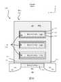
圖2示出在基板之上形成的電晶體200的實例。電晶體200可以包括環繞式閘極(GAA)場效應電晶體(FET)。具體地,電晶體200包括多溝道環繞式閘極FET。電晶體200可以被配置為(i)負溝道金屬氧化物半導體(NMOS)電晶體,或者(ii)正溝道金屬氧化物半導體(PMOS)電晶體。如下文將進一步描述的,互補金屬氧化物半導體(CMOS)結構可以由被配置為NMOS電晶體的第一電晶體(例如,200)和被配置為PMOS電晶體的第二電晶體(例如,200)來定義。電晶體200可以是電晶體構件(例如,第一電晶體構件、第二電晶體構件)。FIG. 2 shows an example of a
如圖2所示,在基板202之上形成電晶體200。基板202可以包括矽(Si)。電晶體200(例如,第一電晶體、第二電晶體)包括源極204(例如,第一源極、第二源極)、汲極206(例如,第一汲極、第二汲極)、閘極208(例如,第一閘極、第二閘極)和多個溝道210(例如,第一多個溝道、第二多個溝道)。在一些實現方式中,基板202可以被認為屬於電晶體200。基板202可以包括一或多個淺溝槽隔離(STI)203。基板202可以是P基板或N基板。儘管未圖示,但是基板202可以包括阱,如P阱和N阱。As shown in FIG. 2 , a
圖2圖示源極204被設置(例如,形成、定位)在基板202之上。類似地,汲極206被設置(例如,形成、定位)在基板202之上。多個溝道210耦合到源極204和汲極206。多個溝道210耦合到源極204和汲極206,使得多個溝道210位於源極204和汲極206之間。多個溝道210被配置為:當在閘極208和基板202之間施加電壓(Vt)時,允許電流在源極204和汲極206之間流動。多個溝道210可以包括第一溝道、第二溝道和第三溝道。第一溝道、第二溝道和第三溝道可以垂直地堆疊在彼此上方,每兩個溝道之間都有(用於閘極的)空間。不同的實現方式可以包括不同數量的溝道210。FIG. 2 illustrates that the
來自多個溝道210當中的一或多個溝道可以包括矽鍺(SiGe)。在一些實現方式中,一或多個溝道可以包括具有在大約百分之2-8(%)的範圍內的鍺(Ge)濃度的矽(Si)。在一些實現方式中,如本案內容中所使用的,濃度百分比可以是Ge的原子數相對於Si的原子數。然而,濃度百分比可能表示別的內容,例如質量。在溝道中添加鍺有助於減小用於在源極204和汲極206之間引起電流所需要的最小電壓(Vt)。在一些實現方式中,針對NMOS電晶體(例如,NFET)可能不存在明顯的Vt變化,但是針對PMOS電晶體(例如,PFET)的Vt可能根據Ge百分比而降低(歸因於SiGe溝道的價帶對Si基板價帶(valence band)的抵消)。因此,電晶體200可以需要較少的能量來操作,並且最終包括電晶體200的元件及/或整合元件亦可以需要較少的能量來操作。用於引起電流所需要的最小電壓(Vt)可以適用於PMOS電晶體及/或NMOS電晶體。在一些實現方式中,對於PMOS電晶體及/或NMOS電晶體,用於引起電流所需要的最小電壓(Vt)大約在0.15-0.3伏(V)的範圍內。可以選擇多個溝道210中的Ge的濃度,以產生用於引起電流的期望最小電壓(Vt)要求。在多個溝道210中的Ge的濃度對於所有多個溝道210可以是相同的,或者溝道210中的一些溝道可以具有不同的Ge濃度。在一些實現方式中,溝道210中的一些溝道可以不具有Ge濃度。應注意的是,對SiGe溝道的使用不限於環繞式閘極FET。包括SiGe的溝道亦可以用在其他類型的FET中。One or more of the channels from the plurality of
閘極208位於源極204和汲極206之間。形成閘極208以便環繞(wrap around)或圍繞(surround)多個溝道210。例如,閘極208可以圍繞來自多個溝道210中的溝道的四個側面。應注意的是,電晶體200的尺寸和形狀是示例性的。此外,所示的電晶體200的一些或全部部件可能不是按比例的。另外,為了清楚的目的,可能在圖2中未圖示所有部件。
如上文所提及,電晶體200可以被配置為作為NMOS電晶體或PMOS電晶體進行操作。為了作為NMOS電晶體進行操作,源極204和汲極206可以均包括N型摻雜劑(N+)。此外,可以在基板中形成的P阱之上形成電晶體200中的至少一些電晶體。為了作為PMOS電晶體進行操作,源極204和汲極206可以均包括P型摻雜劑(P+)。此外,可以在基板中形成的N阱之上形成電晶體200中的至少一些電晶體。下文至少在圖7-12中進一步描述了電晶體200可以如何被配置為作為NMOS電晶體或PMOS電晶體進行操作的實例。如下文將進一步描述的,被配置為作為NMOS電晶體進行操作的第一電晶體以及被配置為作為PMOS電晶體進行操作的第二電晶體可以用於形成和定義整合元件中的CMOS結構。As mentioned above, the
圖3圖示被閘極圍繞的多個溝道的示例性視圖。在一些實現方式中,可以經由在溝道和閘極之間的一層或多層材料來將電晶體的多個溝道與閘極分開。在一些實現方式中,該等層可以被認為屬於閘極。此外,一層或多層材料可以位於閘極208和基板202之間。3 illustrates an exemplary view of multiple channels surrounded by gates. In some implementations, multiple channels and gates of a transistor may be separated via one or more layers of material between the channel and gate. In some implementations, these layers may be considered to belong to the gate. Additionally, one or more layers of material may be located between the
圖3圖示在基板202之上形成閘極208。基板202包括STI 203。可以在STI 203之上形成閘極208中的一些閘極。圖3圖示在閘極208和基板202之間存在一或多個層。圖3圖示在閘極208和基板202之間的第一層311、第二層313和第三層315。第一層311可以包括高介電常數介電層,第二層313可以包括第一金屬層(例如,氮化鈦(Tin)),並且第三層315可以是功函數(work function)金屬層(例如,TiAlxCy)。高介電常數介電層可以包括HfO、HfSiO、HfSiON、HfLaO、HfLaSiO、HfLaSiON、HfAlO、HfAlSiO、HfAlSiON,及/或其組合。功函數金屬層可以包括TiN、TaN、TiAl(C)、TiAlxCy、W及/或其組合。閘極208可以包括低電阻金屬(例如,鎢)。在一些實現方式中,第一層311、第二層313及/或第三層315可以被認為屬於閘極208。FIG. 3 illustrates the formation of
閘極208圍繞多個溝道210(例如,210a、210b、210c)。在閘極208和多個溝道210(例如,210a、210b、210c)之間可以存在一層或多層。例如,在閘極208和多個溝道210(例如,210a、210b、210c)之間可以存在第一層311、第二層313及/或第三層315。各個層(例如,311、313、315)的厚度可以變化。例如,第一層311可以具有在1-3奈米(nm)的範圍內的厚度,第二層313可以具有在1-4 nm的範圍內的厚度,並且第三層315可以具有在1-5 nm的範圍內的厚度。在一些實現方式中,各個層的厚度的變化可以基於電晶體200是被配置為作為NMOS電晶體還是PMOS電晶體進行操作來改變。應注意的是,一些實現方式可能不包括上述層(例如,第一層311、第二層313、第三層315)中的所有層。在一些實現方式中,可能存在額外的層。The
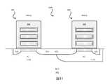
圖4圖示整合元件的單元400。單元400可以表示整合元件的元件層級單元。在圖15中進一步描述了整合元件。如圖4所示,單元400包括由NMOS電晶體402(例如,第一電晶體)和PMOS電晶體404(例如,第二電晶體)定義的CMOS結構401。NMOS電晶體402可以是電晶體200,其中源極和汲極包括N型摻雜劑(N+)。類似地,PMOS電晶體404可以是電晶體200,其中源極和汲極包括P型摻雜劑(P+)。NMOS電晶體402和PMOS電晶體404可以共享相同的閘極或者具有不同的閘極。下文在圖7-12中進一步描述了NMOS電晶體和PMOS電晶體的更詳細的實例。如下文進一步描述的,整合元件可以包括多個單元400,每個單元具有CMOS結構、NMOS電晶體及/或PMOS電晶體的相同或不同的佈置。FIG. 4 illustrates a
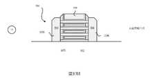
圖5圖示電晶體500的剖面圖。圖5的電晶體500可以表示圖2的電晶體200的整個截面AA的視圖。如圖5所示,在基板502之上形成電晶體500。基板502可以包括矽(Si)。基板502可以是P基板、N基板或未被摻雜的。電晶體500包括源極504、汲極506、閘極508和多個溝道510(例如,510a、510b、510c)。在一些實現方式中,基板502可以被認為屬於電晶體500。儘管未圖示,但是基板502可以包括阱,例如P阱和N阱。FIG. 5 illustrates a cross-sectional view of
圖5圖示源極504被設置(例如,形成、定位)在基板502之上。類似地,汲極506被設置(例如,形成、定位)在基板502之上。多個溝道510耦合到源極504和汲極506。多個溝道510位於源極504和汲極506之間。多個溝道510被配置為:當在閘極508和基板502之間施加電壓(Vt)時,允許電流在源極504和汲極506之間流動。多個溝道510可以包括第一溝道510a、第二溝道510b和第三溝道510c。第一溝道510a、第二溝道510b和第三溝道510c可以垂直地堆疊在彼此上方,每兩個溝道之間都有(用於閘極的)空間。不同的實現方式可以包括不同數量的溝道510。FIG. 5 illustrates that the
來自多個溝道510中的一或多個溝道可以包括矽鍺(SiGe)。在一些實現方式中,一或多個溝道可以包括具有在大約百分之2-8(%)的範圍內的鍺(Ge)濃度的矽(Si)。在一些實現方式中,來自第一多個溝道510之每一者溝道具有大約5-10奈米(nm)的溝道厚度。在一些實現方式中,在溝道之間的垂直空間或間隙大約為7-20奈米(nm)。One or more channels from the plurality of
閘極508位於源極504和汲極506之間。形成閘極508以便環繞或圍繞多個溝道510。例如,閘極508可以圍繞來自多個溝道510中的溝道的四個側面。電晶體500亦包括間隙壁516和內部間隙壁518。間隙壁516及/或內部間隙壁518可以包括SiO、SiN、SiON、SiC及/或其組合。
圖5圖示在閘極508和多個溝道510(例如,510a、510b、510c)之間存在一層或多層。例如,在閘極508和多個溝道510(例如,510a、510b、510c)之間可以存在第一層511、第二層513及/或第三層515。各個層(例如,511、513、515)的厚度可以變化。第一層511可以被設置在多個溝道510之上。第二層513可以被設置在第一層511之上。第三層515可以被設置在第二層513之上。第一層511可以包括高介電常數介電層。高介電常數介電層可以包括HfO、HfSiO、HfSiON、HfLaO、HfLaSiO、HfLaSiON、HfAlO、HfAlSiO、HfAlSiON,及/或其組合。第二層513可以包括第一金屬層(例如,氮化鈦(Tin))。第三層515可以是功函數金屬層(例如,TiAlxCy)。功函數金屬層可以包括TiN、TaN、TiAl(C)、TiAlxCy、W及/或其組合。閘極508可以包括低電阻金屬(例如,鎢)。如上所提到的,第一層511、第二層513和第三層517可以被認為屬於閘極。5 illustrates that one or more layers are present between the
圖6圖示電晶體500的另一剖面圖。圖6的電晶體500可以表示圖2的電晶體200的整個截面BB的視圖。圖6圖示在閘極508和基板502之間存在一層或多層。具體地,在閘極508和基板502之間存在第一層511、第二層513和第三層515。第一層511可以位於基板502之上(例如,STI 503之上)。第二層513可以位於第一層511之上。第三層515可以位於第二層513之上。閘極508可以位於第三層515之上。FIG. 6 illustrates another cross-sectional view of
圖5和6圖示底部SiGe層512。在一些實現方式中,底部SiGe層512可以被認為屬於多個溝道510,此取決於底部SiGe層512是否耦合到源極504和汲極506。底部SiGe層512可以被認為屬於基板502,或者底部SiGe層512可以被認為是位於基板502之上。應注意的是,電晶體500的尺寸和形狀是示例性的。此外,所示的電晶體500的一些或全部部件可能不是按比例的。另外,電晶體500的各種部件的放置及/或位置可以變化。5 and 6 illustrate the
如上所提到的,電晶體可以被配置為作為NMOS電晶體或PMOS電晶體進行操作。圖7-12圖示NMOS電晶體和PMOS電晶體的實例。在一些實現方式中,各個層(例如,311、313、315)的厚度的變化可以基於電晶體是被配置為作為NMOS電晶體還是PMOS電晶體進行操作而變化。As mentioned above, the transistors may be configured to operate as NMOS transistors or PMOS transistors. 7-12 illustrate examples of NMOS transistors and PMOS transistors. In some implementations, the variation in thickness of the various layers (eg, 311 , 313 , 315 ) may vary based on whether the transistor is configured to operate as an NMOS transistor or a PMOS transistor.
圖7圖示電晶體700的示例性剖面圖。圖7的電晶體700可以表示圖2的電晶體200的整個截面AA的視圖。電晶體700可以類似於圖5的電晶體500,並且因此包括與電晶體500相同或相似的部件。電晶體700被配置為作為負溝道金屬氧化物半導體(NMOS)電晶體進行操作。圖7圖示電晶體700包括源極704和汲極706。源極704類似於源極504。汲極706類似於汲極506。源極704和汲極706均包括N型摻雜劑(N+)。儘管未圖示,但是可以在基板502的P阱或N阱之上形成電晶體700。基板502可以是P基板或N基板。如圖7所示,電晶體700包括層511、第二層713和第三層515。除了第二層713較薄之外,第二層713類似於如在圖5中描述的第二層513。在一些實現方式中,第二層713具有大約1-3奈米(nm)的厚度。FIG. 7 illustrates an exemplary cross-sectional view of
圖8圖示電晶體700的示例性剖面圖。圖8的電晶體700可以表示圖2的電晶體200的整個截面BB的視圖。電晶體700可以類似於圖6的電晶體500,並且因此包括與電晶體500相同或相似的部件。如圖8所示,電晶體700包括層511、第二層713和第三層515。除了第二層713較薄之外,第二層713類似於如在圖5中描述的第二層513。FIG. 8 illustrates an exemplary cross-sectional view of
圖9圖示電晶體900的示例性剖面圖。圖9的電晶體900可以表示圖2的電晶體200的整個截面AA的視圖。電晶體900可以類似於圖5的電晶體500,並且因此包括與電晶體500相同或相似的部件。電晶體900被配置為作為正溝道金屬氧化物半導體(PMOS)電晶體進行操作。圖9圖示電晶體900包括源極904和汲極906。源極904類似於源極504。汲極906類似於汲極506。源極904和汲極906均包括P型摻雜劑(P+)。儘管未圖示,但是可以在基板502的N阱或P阱之上形成電晶體900。基板502可以是P基板或N基板。如圖9所示,電晶體900包括層511、第二層913和第三層515。除了第二層913較厚之外,第二層913類似於如在圖5中描述的第二層513。在一些實現方式中,第二層913具有大約2-4奈米(nm)的厚度。FIG. 9 illustrates an exemplary cross-sectional view of
圖10圖示電晶體900的示例性剖面圖。圖10的電晶體900可以表示圖2的電晶體200的整個截面BB的視圖。電晶體900可以類似於圖6的電晶體500,並且因此包括與電晶體500相同或相似的部件。如圖10所示,電晶體900包括層511、第二層913和第三層515。除了第二層913較厚之外,第二層913類似於如在圖9中描述的第二層513。FIG. 10 illustrates an exemplary cross-sectional view of
在一些實現方式中,可以形成NMOS電晶體和PMOS電晶體以作為互補金屬氧化物半導體(CMOS)進行操作。圖11圖示在基板502之上形成的第一結構1100。第一結構1100包括電晶體700和電晶體900。電晶體700可以是被配置為作為NMOS進行操作的第一電晶體,並且電晶體900可以是被配置為作為PMOS進行操作的第二電晶體。電晶體700是在P阱1120之上形成的,而電晶體900是在N阱1130之上形成的。電晶體700和電晶體900兩者皆包括其自身相應的閘極508(例如,用於電晶體700的第一閘極、用於電晶體900的第二閘極)。在一些實現方式中,第一結構1100可以被配置為作為互補金屬氧化物半導體(CMOS)結構進行操作。P阱1120可以表示基板502。例如,基板502可以是P基板(摻雜有P型摻雜劑的基板)。替代地,基板502可以是N基板(摻雜有N型摻雜劑的基板),並且在N基板502中形成P阱。In some implementations, NMOS transistors and PMOS transistors can be formed to operate as complementary metal oxide semiconductors (CMOS). FIG. 11 illustrates a
圖12圖示CMOS的另一種實現方式。圖12圖示在基板502之上形成的第二結構1200。第二結構1200包括電晶體700和電晶體900。電晶體700可以是被配置為作為NMOS進行操作的第一電晶體,並且電晶體900可以是被配置為作為PMOS進行操作的第二電晶體。電晶體700是在P阱1220之上形成的,而電晶體900是在N阱1230之上形成的。P阱1220可以表示基板502。例如,基板502可以是P基板(摻雜有P型摻雜劑的基板)。替代地,基板502可以是N基板(摻雜有N型摻雜劑的基板),並且在N基板502中形成P阱。Figure 12 illustrates another implementation of CMOS. FIG. 12 illustrates the
如圖12所示,電晶體700和電晶體900共享相同的閘極1208。因此,例如,電晶體700可以包括第一閘極,並且電晶體900可以包括第二閘極,其中第一閘極和第二閘極屬於同一閘極1208。在一些實現方式中,第二結構1200可以被配置為作為互補金屬氧化物半導體(CMOS)結構進行操作。應注意的是,在該實例中,被施加到閘極1208的電壓(其是足夠高的)可以在第二結構1200的電晶體700和電晶體900兩者中引起電流。在該實例中,被施加到閘極1208的最低可能電壓必須足夠高,以滿足兩個電晶體(700、900)的最小電壓要求。因此,若一個電晶體具有與另一個電晶體不同的、用於引起電流的最小電壓要求,則將使用較高的最小電壓要求。在一些實現方式中,在電晶體的溝道中使用矽鍺(SiGe)允許NMOS電晶體和PMOS電晶體兩者皆具有用於引起電流的較低的最小電壓要求。As shown in FIG. 12,
已經描述了包括NMOS電晶體和PMOS電晶體的各種電晶體,現在將在下文描述用於製造一或多個電晶體的序列。Having described various transistors including NMOS transistors and PMOS transistors, the sequence for fabricating one or more transistors will now be described below.
用於製造包括具有矽鍺(SiGe)的溝道的電晶體的示例性序列Exemplary Sequence for Fabricating a Transistor Including a Channel with Silicon Germanium (SiGe)
在一些實現方式中,製造電晶體(例如,NMOS電晶體或PMOS電晶體)包括數個製程。圖13(其包括圖13A-13H)圖示用於提供或製造電晶體的示例性序列。在一些實現方式中,圖13A-13H的序列可以用於提供或製造圖2、3、5-12的電晶體及/或在本案內容中描述的其他電晶體。應注意的是,用於製造電晶體的序列可以用於提供或製造具有NMOS電晶體和PMOS電晶體的CMOS結構。另外,用於製造電晶體的序列可以用於同時製造數個電晶體(例如,NMOS電晶體、PMOS電晶體)。然而,為了清楚的目的,圖13的序列圖示對一個電晶體的製造。In some implementations, fabricating a transistor (eg, an NMOS transistor or a PMOS transistor) involves several processes. Figure 13, which includes Figures 13A-13H, illustrates an exemplary sequence for providing or fabricating a transistor. In some implementations, the sequence of Figures 13A-13H may be used to provide or fabricate the transistors of Figures 2, 3, 5-12 and/or other transistors described in this context. It should be noted that the sequence used to fabricate the transistors can be used to provide or fabricate CMOS structures with NMOS transistors and PMOS transistors. Additionally, the sequence used to fabricate transistors can be used to fabricate several transistors simultaneously (eg, NMOS transistors, PMOS transistors). However, for the sake of clarity, the sequence of Figure 13 illustrates the fabrication of one transistor.
應當注意的是,圖13A-13H的序列可能將一或多個階段合併,以便簡化及/或闡明用於提供或製造電晶體的序列。在一些實現方式中,可以改變或修改該等製程的次序。在一些實現方式中,在不脫離本案內容的精神的情況下,可以替換或替代製程中的一或多個製程。It should be noted that the sequence of Figures 13A-13H may incorporate one or more stages in order to simplify and/or clarify the sequence for providing or fabricating the transistor. In some implementations, the order of the processes may be changed or modified. In some implementations, one or more of the processes may be substituted or substituted without departing from the spirit of the present disclosure.
如圖13A所示,階段1圖示在提供基板502之後的狀態。不同的實現方式可以為基板502提供不同的材料。在一些實現方式中,基板502可以包括矽(Si)。階段1亦可以示出在基板502中形成一或多個阱(例如,P阱、N阱)之後的狀態。阱形成可以包括離子形成或擴散製程。在一些實現方式中,基板502可已經包括摻雜劑。例如,若基板502是P基板,則可以在基板502中形成N阱。若基板502是N基板,則可以在基板502中形成P阱。在一些實現方式中,可以使用氧化、光阻劑、遮罩、光阻劑移除、蝕刻(例如,酸蝕刻)和阱形成來提供基板502。為了清楚的目的,未圖示阱。As shown in FIG. 13A,
階段2圖示在超晶格形成之後的狀態。在一些實現方式中,超晶格形成包括:在基板502之上形成低矽鍺(SiGe)層1302和高矽鍺(SiGe)層1303的交替層的堆疊結構,並且經由移除(例如,蝕刻、乾式蝕刻、濕式蝕刻)堆疊結構的部分來從堆疊結構中產生一或多個超晶格1301。低矽鍺(SiGe)層1302在圖中可以被表示為SiGe*。低SiGe層1302可以包括具有在大約2%-8%的範圍內的濃度的鍺。高矽鍺(SiGe)層1303在圖中可以被表示為SiGe**。高SiGe層1303可以包括具有在大約30%-50%的範圍內的濃度的鍺。然而,不同的實現方式可以針對低SiGe層1302及/或高SiGe層1303使用不同的Ge濃度。
形成堆疊結構的製程可以包括使用磊晶製程。製造超晶格的製程可以包括製造一或多個淺溝槽隔離(STI)(其未被示出)。超晶格形成亦可以包括鰭露出製程(fin reveal process),其中移除STI的部分,從而暴露超晶格及/或鰭的至少一些部分。The process of forming the stacked structure may include using an epitaxial process. The process of fabricating the superlattice may include fabricating one or more shallow trench isolations (STIs) (not shown). Superlattice formation may also include a fin reveal process in which portions of the STI are removed, thereby exposing at least some portions of the superlattice and/or fins.
如圖13B所示,階段3圖示在虛設閘極和間隙壁形成之後的狀態。在超晶格1301之上(例如,在頂部低SiGe層之上)形成氧化層1310。在氧化層1310和超晶格1301之上形成虛設閘極1320。此外,在超晶格1301之上形成間隙壁1316。更具體地,在超晶格1301之上並且與虛設閘極1320相鄰(並且在虛設閘極1320的每一側)形成間隙壁1316。應注意的是,間隙壁1316是示例性的。在一些實現方式中,間隙壁1316可以是間隙壁516,或者是在本案內容中描述的任何間隙壁。可以使用化學氣相沉積(CVD)製程及/或原子層沉積(ALD)製程來形成虛設閘極及/或間隙壁。As shown in FIG. 13B,
階段4圖示在空腔蝕刻之後的狀態。在空腔蝕刻之後,移除超晶格1301的未被虛設閘極1320及/或間隙壁1316覆蓋的部分。空腔蝕刻可以涉及移除超晶格1301的低SiGe層1302的部分和高SiGe層1303的部分。
如圖13C所示,階段5圖示在SiGe凹槽之後的狀態。在SiGe凹槽之後,高SiGe層1303的在間隙壁1316下方的部分被移除。As shown in Figure 13C,
階段6圖示在內部間隙壁形成之後的狀態。在內部間隙壁形成之後,在先前移除高SiGe層1303的空腔中形成內部間隙壁1318(如階段5所示)。在一些實現方式中,內部間隙壁1318可以是內部間隙壁518,或者是在本案內容中描述的任何間隙壁。Stage 6 illustrates the state after the formation of the internal spacer. After the internal spacers are formed,
如圖13D所示,階段7圖示在源極和汲極形成之後的狀態。在源極和汲極形成之後,在基板502之上形成源極和汲極。例如,第一源極504和第一汲極506被設置在基板502之上。As shown in Figure 13D,
階段8圖示在摻雜源極和汲極之後的狀態。源極504和汲極506可以摻雜有N型摻雜劑(N+)或P型摻雜劑(P+)。利用N型摻雜劑(N+)來摻雜源極504和汲極506可以產生圖7的源極704和汲極706。利用P型摻雜劑(P+)來摻雜源極504和汲極506可以產生源極904和汲極906。氣相磊晶可以用於摻雜源極和汲極。然而,不同的實現方式可以使用不同的製程來摻雜源極和汲極。
如圖13E所示,階段9圖示在層間電媒體(ILD)形成之後的狀態。在ILD形成之後,在源極304、汲極306和間隙壁1316之上形成氧化層1340。在氧化層1340之上進一步形成介電層1350。As shown in Figure 13E,
階段10圖示在虛設閘極和虛設介電層移除之後的狀態,其中移除了虛設閘極1320和氧化層1310,從而暴露頂部低SiGe層1302的部分。
如圖13F所示,階段11圖示在高SiGe層移除之後的狀態,其中移除了(例如,蝕刻掉)超晶格1301的高SiGe層1303,從而在低SiGe層1302之間留下空腔。As shown in FIG. 13F ,
階段12圖示在高介電常數介電層形成之後的狀態,其中在先前被高SiGe層1303佔據的空腔中,在間隙壁1316之間形成高介電常數介電層。高介電常數介電層可以是如圖5中描述的第一層511。可以使用沉積製程來形成高介電常數介電層。然而,不同的實現方式可以以不同的方式來形成高介電常數介電層。為了清楚的目的,未圖示氧化層1340和介電層1350。
如圖13G所示,階段13圖示在第二層形成之後的狀態,其中在高介電常數介電層之上形成第二層513。第二層513可以包括TiN或者在本案內容中描述的任何其他材料。可以使用沉積製程來形成第二層513。然而,不同的實現方式可以以不同的方式來形成第二層。As shown in FIG. 13G,
階段14圖示在功金屬形成之後的狀態,其中在第二層513上形成第三層515。第三層515可以包括金屬。第三層515的實例包括TaN、TiA(C)、TiAlxCy、W及/或其組合。可以使用沉積製程來形成第三層515。然而,不同的實現方式可以以不同的方式來形成第三層。
如圖13H所示,階段15圖示在金屬閘極形成之後的狀態。在金屬閘極形成之後,在第三層515之上形成金屬部件(例如,閘極508)。金屬部件可以位於先前被高SiGe層1303佔據的空腔內。金屬部件可以定義閘極508,或者在本案內容中描述的任何閘極。為了清楚的目的,未圖示氧化層1340和介電層1350。階段15可以示出圖5的電晶體500,並且根據對源極和汲極的摻雜,示出電晶體700(例如,NMOS電晶體)或電晶體900(例如,PMOS電晶體)。在一些實現方式中,可以在電晶體上執行額外的製程,包括拋光製程。As shown in Figure 13H,
用於製造包括具有矽鍺(SiGe)的溝道的電晶體的方法的示例性流程圖Exemplary flow diagram of a method for fabricating a transistor including a channel with silicon germanium (SiGe)
在一些實現方式中,製造電晶體包括數個製程。圖14圖示用於提供或製造電晶體(例如,NMOS電晶體或PMOS電晶體)的方法1400的示例性流程圖。電晶體可以是形成CMOS結構的電晶體的部分。在一些實現方式中,圖14的方法1400可以用於提供或製造圖2、圖5-12的電晶體及/或在本案內容中描述的其他電晶體。In some implementations, fabricating a transistor includes several processes. 14 illustrates an exemplary flow diagram of a
應當注意的是,圖14的序列可能將一或多個製程組合,以便簡化及/或闡明用於提供或製造電晶體的方法。在一些實現方式中,可以改變或修改製程的次序。It should be noted that the sequence of Figure 14 may combine one or more processes in order to simplify and/or clarify a method for providing or fabricating a transistor. In some implementations, the order of the processes may be changed or modified.
該方法在基板502之上形成(在1405處)低矽鍺(SiGe)和高矽鍺(SiGe)的交替層的堆疊結構。可以在基板502之上形成堆疊結構。不同的實現方式可以為基板502提供不同的材料。在一些實現方式中,基板502可以包括矽(Si)。基板502可以包括P基板或N基板。在一些實現方式中,基板502未被摻雜。基板502可以包括阱(例如,N阱、P阱)。The method forms (at 1405 ) a stack of alternating layers of low silicon germanium (SiGe) and high silicon germanium (SiGe) over
該方法從堆疊結構形成(在1410處)超晶格(例如,1301)。可以經由移除(例如,蝕刻)堆疊結構的部分來形成超晶格。形成超晶格的製程可以包括在超晶格1301周圍形成淺溝槽隔離(STI),以及經由移除STI的部分來暴露超晶格1301。The method forms (at 1410) a superlattice (eg, 1301) from the stacked structure. The superlattice may be formed by removing (eg, etching) portions of the stack structure. The process of forming the superlattice may include forming shallow trench isolation (STI) around the
該方法形成(在1415處)虛設閘極和間隙壁,其中在超晶格1301之上(例如,在頂部低SiGe層之上)形成氧化層1310,並且在氧化層1310和超晶格1301之上形成虛設閘極1320。另外,在超晶格1301之上形成間隙壁1316。更具體地,在超晶格1301之上並且與虛設閘極1320相鄰處(並且在虛設閘極1320的每一側)形成間隙壁1316。應注意的是,間隙壁1316是示例性的。在一些實現方式中,間隙壁1316可以是間隙壁516,或者在本案內容中描述的任何間隙壁。The method forms (at 1415 ) dummy gates and spacers, wherein
該方法執行(在1420處)空腔蝕刻、高SiGe凹槽形成和內部間隙壁形成。在空腔蝕刻期間,移除超晶格1301的未被虛設閘極1320及/或間隙壁1316覆蓋的部分。空腔蝕刻涉及移除超晶格1301的高SiGe層1303的部分。在高SiGe凹槽形成期間,移除高SiGe層的在間隙壁1316下方的部分。在內部間隙壁形成期間,在其中先前移除高SiGe層1303的空腔中形成內部間隙壁1318。The method performs (at 1420) cavity etching, high SiGe groove formation, and internal spacer formation. During the cavity etch, portions of the
該方法形成(在1425處)源極和汲極,並且執行層間電媒體(ILD)形成。形成源極和汲極可以包括在基板502(及/或阱)之上設置(例如,形成)源極504和汲極506。形成源極和汲極亦可以包括對源極和汲極進行摻雜。例如,源極504和汲極506可以摻雜有N型摻雜劑(N +)或P型摻雜劑(P+)。利用N型摻雜劑(N +)來摻雜源極504和汲極506可以產生源極704和汲極706。利用P型摻雜劑(P +)來摻雜源極504和汲極506可以產生源極904和汲極906。ILD形成可以包括在源極504、汲極506和間隙壁516之上形成氧化層1340。ILD形成亦可以包括在氧化層1340之上形成介電層1350。The method forms (at 1425) source and drain electrodes, and performs interlayer dielectric (ILD) formation. Forming the source and drain may include disposing (eg, forming) a
該方法執行(在1430處)虛設閘極移除,其中移除虛設閘極1320和氧化層1310,從而暴露頂部低SiGe層1302的部分。此外,該方法亦可以執行虛設SiGe移除,其中移除超晶格1301的高SiGe層1303,從而在低SiGe層1302之間留下空腔。可以使用一或多個蝕刻製程來移除虛設閘極和高SiGe層。The method performs (at 1430 ) dummy gate removal, wherein
該方法執行(在1435處)高介電常數介電層形成、TiN形成、功金屬形成和閘極形成。在高介電常數介電層形成期間,在先前被高SiGe層1303佔據的空腔中,在間隙壁1316之間,在低SiGe層1302之上形成第一層511(例如,高介電常數介電層)。該方法亦可以在第一層511之上形成第二層513。第二層513可以包括TiN。在功金屬形成期間,可以在第二層513之上形成第三層515。在閘極形成期間,在第三層515之上形成金屬部件。金屬部件可以定義閘極508。The method performs (at 1435) high-k dielectric layer formation, TiN formation, work metal formation, and gate formation. During the formation of the high-k dielectric layer, in the cavity previously occupied by the high-
該方法在電晶體上方形成(在1440處)互連。互連可以耦合到閘極508、源極504及/或汲極506。The method forms (at 1440) interconnects over the transistors. The interconnect may be coupled to
包括包含具有矽鍺(SiGe)的溝道的電晶體的示例性整合元件Exemplary integrated elements including transistors with channels having silicon germanium (SiGe)
圖15圖示整合元件1500的剖面圖,整合元件1500包括一或多個電晶體,一或多個電晶體包括具有矽鍺(SiGe)的溝道。整合元件1500包括基板1520、多個元件層級單元1522(例如,邏輯單元)、互連部分1504和封裝部分1506。多個元件層級單元1522是在基板1520之上形成的。元件層級單元1522可以形成整合元件1500的元件層級層。在一些實現方式中,多個元件層級單元1522可以包括基板1520的部分。在一些實現方式中,基板1520和多個元件層級單元1522可以被稱為整合元件1500的基板部分1502。15 illustrates a cross-sectional view of an
多個元件層級單元1522可以包括NMOS電晶體、PMOS電晶體及/或CMOS結構,其中至少一個電晶體包括具有矽鍺(SiGe)的溝道。多個元件層級單元1522可以包括如在圖4中描述的單元400。如圖15所示,元件層級單元中的一個元件層級單元包括結構1100(例如,CMOS結構),該結構1100包括NMOS電晶體700和PMOS電晶體900。NMOS電晶體700及/或PMOS電晶體900可以包括溝道,該溝道包括矽鍺(SiGe)。The plurality of
在一些實現方式中,NMOS電晶體700可以是在基板1520之上形成的第一電晶體(例如,第一電晶體構件)。在一些實現方式中,電晶體700可以包括:被設置在基板1520之上的源極704(例如,第一源極);被設置在基板1520之上的汲極706(例如,第一汲極);耦合到源極704和汲極706的多個溝道510(例如,第一多個溝道)。多個溝道510位於源極之間704和汲極706之間。來自多個溝道510中的至少一個溝道包括矽鍺(SiGe)。電晶體700可以包括圍繞多個溝道510的第一閘極(例如,508、1208)。In some implementations,
在一些實現方式中,PMOS電晶體900可以是在基板1520之上形成的第二電晶體(例如,第二電晶體構件)。在一些實現方式中,電晶體900可以包括:被設置在基板1520之上的源極904(例如,第二源極);被設置在基板1520之上的汲極906(例如,第二汲極);耦合到源極904和汲極906的多個溝道510(例如,第二多個溝道)。多個溝道510位於源極904和汲極906之間。來自多個溝道510中的至少一個溝道包括矽鍺(SiGe)。電晶體900可以包括圍繞多個溝道510的第二閘極(例如,508、1208)。在一些實現方式中,電晶體700和電晶體900可以共享相同的閘極。In some implementations, the
不同的實現方式可以具有不同數量及/或佈置的CMOS結構、NMOS電晶體及/或PMOS電晶體。CMOS結構1100可以是CMOS結構401。應注意的是,整合元件1500可以包括其他類型的結構,例如圖12的結構1200。Different implementations may have different numbers and/or arrangements of CMOS structures, NMOS transistors, and/or PMOS transistors.
互連部分1504是在基板部分1502之上形成的。具體地,互連部分1504是在多個元件層級單元1522之上形成的。互連部分1504包括佈線層。互連部分1504包括多個互連1540(例如,跡線、焊盤、通孔)和至少一個介電層1542。互連部分1504可以在多個CMOS結構、NMOS電晶體及/或PMOS電晶體之間提供互連。
封裝部分1506是在互連部分1504之上形成的。封裝部分1506包括鈍化層1560、凸塊下金屬化(under bump metallization, UBM)層1562和焊料互連1564。應注意的是,整合元件1500的尺寸和形狀是示例性的。此外,所示的整合元件1500的部件可能不是按比例的。
用於製造包括包含具有矽鍺(SiGe)的溝道的電晶體的整合元件的示例性序列Exemplary Sequence for Fabrication of Integrated Elements Including Transistors Containing Channels with Silicon Germanium (SiGe)
在一些實現方式中,製造包括包含具有矽鍺(SiGe)的溝道的電晶體的整合元件包括數個製程。圖16(其包括圖16A-16B)圖示用於提供或製造包括NMOS電晶體和PMOS電晶體的整合元件的示例性序列,其中電晶體的溝道中的至少一個溝道包括矽鍺(SiGe)。在一些實現方式中,圖16A-16B的序列可以用於提供或製造圖15的整合元件及/或在本案內容中描述的其他整合元件。In some implementations, fabricating an integrated element including a transistor including a channel with silicon germanium (SiGe) includes several processes. 16, which includes FIGS. 16A-16B, illustrates an exemplary sequence for providing or fabricating an integrated element including an NMOS transistor and a PMOS transistor, wherein at least one of the channels of the transistor includes silicon germanium (SiGe) . In some implementations, the sequences of FIGS. 16A-16B can be used to provide or fabricate the integrated elements of FIG. 15 and/or other integrated elements described in this context.
應當注意的是,圖16A-16B的序列可能將一或多個階段合併,以便簡化及/或闡明用於提供或製造包括NMOS電晶體和PMOS電晶體的整合元件的序列,其中電晶體的溝道中的至少一個溝道包括矽鍺(SiGe)。在一些實現方式中,可以改變或修改製程的次序。在一些實現方式中,在不脫離本案內容的精神的情況下,可以替換或替代製程中的一或多個製程。It should be noted that the sequence of FIGS. 16A-16B may combine one or more stages in order to simplify and/or clarify the sequence for providing or fabricating integrated components including NMOS transistors and PMOS transistors, where the channels of the transistors are At least one of the channels includes silicon germanium (SiGe). In some implementations, the order of the processes may be changed or modified. In some implementations, one or more of the processes may be substituted or substituted without departing from the spirit of the present disclosure.
如圖16A所示,階段1圖示在提供基板1520之後的狀態。不同的實現方式可以為基板1520提供不同的材料。在一些實現方式中,基板1520可以包括矽(Si)。基板可以包括阱(例如,N阱、P阱)。As shown in FIG. 16A,
階段2圖示在基板1520之上形成元件層級層之後的狀態。元件層級層包括多個元件層級層單元1522(例如,400)。因此,階段2圖示在基板1520之上形成多個元件級單元1522之後的狀態。在一些實現方式中,可以使用前端(FEOL)製程來製造元件層級層(例如,多個元件層級單元1522)。如前述,來自多個元件層級單元中的一或多個單元可以包括NMOS電晶體及/或PMOS電晶體。電晶體中的一或多個電晶體可以包括具有矽鍺(SiGe)的溝道。圖13A-13H圖示用於製造電晶體(例如,NMOS電晶體、PMOS電晶體)的序列。在一些實現方式中,可以在一或多個電晶體的閘極、源極及/或汲極之上形成互連。
階段3圖示在形成互連部分1504之後的狀態。互連部分1504可以包括多個互連1540和至少一個介電層1542。在一些實現方式中,可以使用後道(BEOL)製程來製造互連部分1504。互連部分1504可以被配置為將一或多個NMOS電晶體、一或多個PMOS電晶體、具有NMOS電晶體和PMOS電晶體的一或多個CMOS結構電耦合。
如圖16B所示,階段4圖示在互連部分1504之上形成鈍化層1560和凸塊下金屬化(UBM)層1562之後的狀態。As shown in FIG. 16B ,
階段5圖示在將焊料互連耦合到凸塊下金屬化(UBM)層1562之後的狀態。階段15可以示出圖15的整合元件1500。
用於製造包括包含具有矽鍺(SiGe)的溝道的電晶體的整合元件的方法的示例性流程圖Exemplary flow diagram of a method for fabricating an integrated element including a transistor having a channel with silicon germanium (SiGe)
在一些實現方式中,提供包括包含具有矽鍺(SiGe)的溝道的電晶體的整合元件包括數個製程。圖17圖示用於提供或製造包括包含具有矽鍺(SiGe)的溝道的電晶體的整合元件的方法1700的示例性流程圖。在一些實現方式中,圖17的方法1700可以用於提供或製造圖15的整合元件及/或在本案內容中描述的其他整合元件。In some implementations, providing an integrated element including a transistor including a channel with silicon germanium (SiGe) involves several processes. 17 illustrates an exemplary flow diagram of a
應當注意的是,圖17的序列可能將一或多個製程組合,以便簡化及/或闡明用於提供或製造包括包含具有矽鍺(SiGe)的溝道的電晶體的整合元件的方法。在一些實現方式中,可以改變或修改製程的次序。It should be noted that the sequence of FIG. 17 may combine one or more processes in order to simplify and/or clarify a method for providing or fabricating an integrated device including a transistor having a channel with silicon germanium (SiGe). In some implementations, the order of the processes may be changed or modified.
該方法提供(在1705處)基板(例如,1520)。不同的實現方式可以為基板提供不同的材料。在一些實現方式中,基板可以包括矽(Si)。基板可以摻雜有N型摻雜劑或P型摻雜劑。提供基板可以包括在基板中形成阱(例如,N阱、P阱)。The method provides (at 1705) a substrate (eg, 1520). Different implementations may provide different materials for the substrate. In some implementations, the substrate can include silicon (Si). The substrate may be doped with N-type dopants or P-type dopants. Providing the substrate may include forming a well (eg, N-well, P-well) in the substrate.
該方法在基板之上形成(在1710處)元件層級層(例如,多個元件層級單元1522)。在一些實現方式中,可以使用前端(FEOL)製程來製造元件層級層(例如,多個元件層級單元1522)。元件層級層可以包括多個元件層級單元(例如,400)。元件層級單元可以包括一或多個主動元件(例如,電晶體)。如在本案內容中所描述的,一或多個元件層級單元可以包括具有NMOS電晶體及/或PMOS電晶體的結構。形成元件層級層可以包括形成一或多個NMOS電晶體(例如,700)及/或一或多個PMOS電晶體(例如,900)。如上所提到的,NMOS電晶體及/或PMOS電晶體可以是環繞式閘極(GAA)電晶體。一或多個電晶體可以包括具有矽鍺(SiGe)的溝道。在一些實現方式中,形成元件層級層包括在基板之上形成第一電晶體。形成第一電晶體可以包括:在基板之上形成的第一源極;在基板之上形成的第一汲極;在第一源極和第一汲極之間形成第一多個溝道,其中來自第一多個溝道中的至少一個溝道包括矽鍺(SiGe)。形成第一電晶體亦可以包括形成圍繞溝道的第一閘極。圖13A-13H圖示在基板之上形成電晶體的實例。The method forms (at 1710 ) a device-level layer (eg, a plurality of device-level cells 1522 ) over a substrate. In some implementations, a front-end (FEOL) process can be used to fabricate the element-level layers (eg, the plurality of element-level cells 1522 ). An element-level layer may include a plurality of element-level units (eg, 400 ). An element-level cell may include one or more active elements (eg, transistors). As described in this context, one or more element level cells may include structures having NMOS transistors and/or PMOS transistors. Forming the element-level layers may include forming one or more NMOS transistors (eg, 700 ) and/or one or more PMOS transistors (eg, 900 ). As mentioned above, the NMOS transistors and/or the PMOS transistors may be gate-all-around (GAA) transistors. The one or more transistors may include a channel having silicon germanium (SiGe). In some implementations, forming the element-level layer includes forming a first transistor over the substrate. Forming the first transistor may include: a first source electrode formed on the substrate; a first drain electrode formed on the substrate; forming a first plurality of channels between the first source electrode and the first drain electrode, Wherein at least one channel from the first plurality of channels includes silicon germanium (SiGe). Forming the first transistor may also include forming a first gate surrounding the channel. 13A-13H illustrate examples of forming transistors over a substrate.
該方法(在1715處)在元件層級層(例如,多個元件層級單元1522)及/或在基板1520之上形成互連部分1504。互連部分1504可以包括多個互連1540和至少一個介電層1542。在一些實現方式中,可以使用後道(BEOL)製程形成互連部分1904。互連部分1504可以被配置為將一或多個電晶體及/或具有NMOS電晶體和PMOS電晶體的一或多個CMOS結構電耦合。The method forms (at 1715 ) the
該方法在互連部分1904之上形成(在1720處)封裝部分1506。封裝部分1506可以包括鈍化層1560和凸塊下金屬化(UBM)層1562。鈍化層1560和凸塊下金屬化(UBM)層1562是在互連部分1504之上形成的。The method forms (at 1720 )
該方法提供(在1725處)焊料互連1564。在一些實現方式中,焊料互連1564耦合到凸塊下金屬化(UBM)層1562。The method provides (at 1725 )
亦應注意的是,圖17的方法1700可以用於製造(例如,同時製造)晶圓上的數個整合元件。隨後將晶圓分離(singulate)(例如,切割)成單獨的整合元件。該等被分離的整合元件隨後可以耦合到其他整合元件及/或印刷電路板(PCB)。It should also be noted that the
示例性電子設備Exemplary Electronics
圖18圖示可以與以下各項中的任何項整合的各種電子設備:上述電晶體、CMOS、NMOS電晶體、PMOS電晶體、元件、整合元件、積體電路(IC)封裝、積體電路(IC)元件、半導體元件、積體電路、晶粒、中介層、封裝或封裝堆疊封裝(package-on-package,PoP)。例如,行動電話設備1802、膝上型電腦設備1804、固定位置終端設備1806,或可穿戴設備1808可以包括如本文描述的元件1800。元件1800可以是例如本文描述的元件及/或積體電路(IC)封裝中的任何一者。在圖18中示出的設備1802、1804、1806和1808僅是示例性的。其他電子設備亦可以特徵在於元件1800,包括但不限於一組設備(例如,電子設備),該組設備包括行動設備、手持個人通訊系統(PCS)單元、可攜式資料單元(諸如個人數位助理)、啟用全球定位系統(GPS)的設備、導航設備、機上盒、音樂播放機、視訊播放機、娛樂設備、固定位置資料單元(如儀錶讀數元件)、通訊設備、智慧手機、平板電腦、電腦、可穿戴設備(例如,手錶、眼鏡)、物聯網路(IoT)設備、伺服器、路由器、在機動車輛(例如,自主車輛)中實現的電子設備,或者儲存或取得資料或電腦指令的任何其他設備,或者其任何組合。Figure 18 illustrates various electronic devices that can be integrated with any of the following transistors, CMOS, NMOS transistors, PMOS transistors, components, integrated components, integrated circuit (IC) packages, integrated circuits ( IC) components, semiconductor components, integrated circuits, dies, interposers, packages or package-on-package (PoP). For example,
在圖2-12、13A-13H、14、15、16A-16B及/或17-18中示出的部件、製程、特徵及/或功能中的一者或多者可以被重新排列及/或組合成單個部件、製程、特徵或功能,或者體現在數個部件、製程或功能中。在不脫離本案內容的情況下,亦可以添加額外的元素、部件、製程及/或功能。亦應當注意的是,圖2-12、13A-13H、14、15、16A-16B及/或17-18以及在本案內容中的其對應描述不限於晶粒及/或IC。在一些實現方式中,圖2-12、13A-13H、14、15、16A-16B及/或17-18以及其對應描述可以用於製造、建立、提供及/或生產元件及/或整合元件。在一些實現方式中,元件可以包括晶粒、整合元件、整合被動元件(IPD)、晶粒封裝、積體電路(IC)元件、元件封裝、積體電路(IC)封裝、晶圓、半導體元件、封裝堆疊封裝(PoP)元件及/或中介層。One or more of the components, processes, features and/or functions shown in Figures 2-12, 13A-13H, 14, 15, 16A-16B and/or 17-18 may be rearranged and/or Combined into a single component, process, feature or function, or embodied in several components, processes or functions. Additional elements, components, processes and/or functions may also be added without departing from the subject matter. It should also be noted that Figures 2-12, 13A-13H, 14, 15, 16A-16B and/or 17-18 and their corresponding descriptions in the context of this application are not limited to dies and/or ICs. In some implementations, Figures 2-12, 13A-13H, 14, 15, 16A-16B and/or 17-18 and their corresponding descriptions may be used to manufacture, build, provide and/or produce elements and/or integrate elements . In some implementations, components may include dies, integrated components, integrated passive components (IPDs), die packages, integrated circuit (IC) components, component packages, integrated circuit (IC) packages, wafers, semiconductor components , Package-on-Package (PoP) components and/or interposers.
注意的是,本案內容中的附圖可以表示各個部分、部件、物件、裝置、封裝、整合元件、積體電路及/或電晶體的實際表示及/或概念表示。在一些情況下,各圖可能不是按比例的。在一些情況下,為了清楚的目的,可能未圖示所有部件及/或部分。在一些情況下,附圖中的各個部分及/或元件的放置、位置、大小及/或形狀可以是示例性的。在一些實現方式中,附圖中的各個元件及/或部分可以是可選的。使用「示例性」一詞意味著「用作示例、實例或說明」。本文中被描述為「示例性的」任何實現方式或態樣未必被解釋為比本案內容的其他態樣優選或具有優勢。同樣,術語「態樣」並不要求本案內容的所有態樣皆包括所論述的特徵、優點或操作模式。本文使用術語「耦合」來代表在兩個物件之間的直接耦合或間接耦合。例如,若物件A在實體上接觸物件B,並且物件B接觸物件C,則物件A和C仍然可以被認為是彼此耦合的,即使其並沒有在實體上彼此直接接觸。亦應注意的是,在本案中在位於一個部件之上的另一個部件的背景下使用的術語「在……之上」可以用於意指在另一個部件上及/或在另一個部件中(例如,在部件的表面上或者被嵌入在部件中)的部件。因此,例如,在第二部件之上的第一部件可以意指(1)第一部件在第二部件之上,但是不直接接觸第二部件,(2)第一部件在第二部件上(例如,在第二部件的表面上),及/或(3)第一部件在第二部件中(例如,被嵌入在第二部件中)。術語蝕刻可以包括乾式蝕刻或濕式蝕刻,並且可以涉及遮罩的使用。形成或設置金屬可以包括電鍍製程、化學氣相沉積(CVP)製程,及/或原子層沉積(ALD)製程。在一些實現方式中,形成一或多個介電層、Si及/或SiGe可以包括一或多個沉積製程。It is noted that the drawings in this context may represent actual and/or conceptual representations of various parts, components, objects, devices, packages, integrated components, integrated circuits and/or transistors. In some instances, the figures may not be to scale. In some instances, not all components and/or sections may be shown for clarity. In some cases, the placement, location, size and/or shape of various parts and/or elements in the figures may be exemplary. In some implementations, various elements and/or portions of the figures may be optional. Use of the word "exemplary" means "serving as an example, instance, or illustration." Any implementation or aspect described herein as "exemplary" is not necessarily to be construed as preferred or advantageous over other aspects of the subject matter. Likewise, the term "aspect" does not require that all aspects of the subject matter include the discussed feature, advantage, or mode of operation. The term "coupled" is used herein to represent direct or indirect coupling between two items. For example, if object A is physically touching object B, and object B is touching object C, then objects A and C can still be considered coupled to each other, even though they are not physically in direct contact with each other. It should also be noted that the term "on" used in this case in the context of one element over another element may be used to mean on and/or in another element (eg, on the surface of the part or embedded in the part). Thus, for example, a first part over a second part may mean (1) the first part is over the second part, but does not directly contact the second part, (2) the first part is on the second part ( For example, on the surface of the second component), and/or (3) the first component is in the second component (eg, embedded in the second component). The term etching may include dry etching or wet etching, and may involve the use of a mask. Forming or disposing the metal may include electroplating processes, chemical vapor deposition (CVP) processes, and/or atomic layer deposition (ALD) processes. In some implementations, forming one or more dielectric layers, Si and/or SiGe, may include one or more deposition processes.
此外,應注意的是,本文中包含的各種公開內容可以被描述為製程,該製程被圖示為流程圖、流程示意圖、結構圖或方塊圖。儘管流程圖可以將操作描述為順序的製程,但是該等操作中的許多操作可以並行或同時執行。另外,可以重新排列操作的次序。製程在其操作完成後被終止。Furthermore, it should be noted that various disclosures contained herein may be described as processes, the processes being illustrated as flow diagrams, schematic flow diagrams, block diagrams, or block diagrams. Although a flowchart may describe the operations as a sequential process, many of the operations may be performed in parallel or concurrently. Additionally, the order of operations can be rearranged. A process is terminated after its operation is complete.
在不脫離本案內容的情況下,可以在不同的系統中實現本文描述的公開內容的各個特徵。應當注意的是,本案內容的前述態樣僅是實例,並且將不被解釋為限制本案內容。對本案內容的各態樣的描述意欲是說明性的,而不是限制請求項的範圍。如此,本文的教導可以容易地應用於其他類型的裝置,並且許多替代、修改和變型對於本領域技藝人士而言將是顯而易見的。Various features of the disclosure described herein may be implemented in different systems without departing from the subject matter. It should be noted that the foregoing aspects of the subject matter are merely examples, and should not be construed as limiting the subject matter. The descriptions of aspects of the subject matter of the present case are intended to be illustrative, not to limit the scope of the claims. As such, the teachings herein may be readily applied to other types of apparatus, and many alternatives, modifications, and variations will be apparent to those skilled in the art.
100:互補金屬氧化物半導體(CMOS)結構102:N阱104:P阱105:基板120:正溝道金屬氧化物半導體(PMOS)電晶體140:負溝道金屬氧化物半導體(NMOS)電晶體140200:電晶體202:基板203:淺溝槽隔離(STI)204:源極206:汲極208:閘極210:多個溝道210a:溝道210b:溝道210c:溝道311:第一層313:第二層315:第三層400:單元401:CMOS結構402:NMOS電晶體404:PMOS電晶體500:電晶體502:基板503:STI504:源極506:汲極508:閘極510:多個溝道510a:溝道510b:溝道510c:溝道511:層512:底部SiGe層513:第二層515:第三層516:間隙壁518:內部間隙壁700:電晶體704:源極713:第二層900:電晶體904:源極906:汲極913:第二層1100:第一結構1120:P阱1130:N阱1200:第二結構1208:閘極1220:P阱1230:N阱1301:超晶格1302:低矽鍺(SiGe)層1303:高SiGe層1310:氧化層1316:間隙壁1318:內部間隙壁1320:虛設閘極1340:氧化層1350:介電層1400:方法1405:步驟1410:步驟1415:步驟1420:步驟1425:步驟1430:步驟1435:步驟1440:步驟1500:整合元件1502:基板部分1504:互連部分1506:封裝部分1520:基板1522:元件層級單元1540:互連1542:介電層1560:鈍化層1562:UBM層1564:焊料互連1700:方法1705:步驟1710:步驟1715:步驟1720:步驟1725:步驟1800:元件1802:行動電話設備1804:膝上型電腦設備1806:固定位置終端設備1808:可穿戴設備100: Complementary Metal Oxide Semiconductor (CMOS) Structures102: N well104:P well105: Substrate120: Positive channel metal oxide semiconductor (PMOS) transistor140: Negative Channel Metal Oxide Semiconductor (NMOS) transistor 140200: Transistor202: Substrate203: Shallow Trench Isolation (STI)204: source206: Drain208: Gate210: Multiple channels210a: Trench210b: Trench210c: Trench311: first floor313: Second Floor315: The third floor400: Unit401: CMOS structure402: NMOS transistor404: PMOS transistor500: Transistor502: Substrate503: STI504: source506: Drain508: Gate510: Multiple channels510a: Trench510b: Trench510c: Trench511: Layer512: Bottom SiGe Layer513: Second floor515: third floor516: Spacer518: Internal Spacer700: Transistor704: Source713: Second floor900: Transistor904: source906: Drain913: Second floor1100: First Structure1120:P well1130: N well1200: Second Structure1208: Gate1220:P well1230: N well1301: Superlattice1302: Low Silicon Germanium (SiGe) Layer1303: High SiGe Layer1310: oxide layer1316: Spacer1318: Internal Spacer1320: Dummy gate1340: oxide layer1350: Dielectric Layer1400: Method1405: Steps1410: Steps1415: Steps1420: Steps1425: Steps1430: Steps1435: Steps1440: Steps1500: Integrated Components1502: Substrate part1504: Interconnect Section1506: Package part1520: Substrate1522: Component level unit1540: Interconnect1542: Dielectric Layer1560: Passivation layer1562: UBM layer1564: Solder Interconnect1700: Method1705: Steps1710: Steps1715: Steps1720: Steps1725: Steps1800: Components1802: Mobile Phone Equipment1804: Laptop Devices1806: Fixed Location Terminal Equipment1808: Wearables
在結合附圖時,根據下文闡述的詳細描述,各種特徵、性質和優點可以變得顯而易見,在附圖中,相同的元件符號始終相應地進行標識。Various features, properties and advantages may become apparent from the detailed description set forth below, when taken in conjunction with the accompanying drawings, wherein like reference numerals are correspondingly identified throughout.
圖1圖示包括正溝道金屬氧化物半導體(PMOS)電晶體和負溝道金屬氧化物半導體(NMOS)電晶體的結構的視圖。1 illustrates a view of a structure including a positive channel metal oxide semiconductor (PMOS) transistor and a negative channel metal oxide semiconductor (NMOS) transistor.
圖2圖示在基板之上形成的環繞式閘極(gate-all-around)場效應電晶體(FET)的示例性視圖。2 illustrates an exemplary view of a gate-all-around field effect transistor (FET) formed over a substrate.
圖3示出圍繞在基板之上形成的溝道的閘極的示例性視圖。3 shows an exemplary view of a gate surrounding a channel formed over a substrate.
圖4圖示包括環繞式閘極FET的整合元件的單元。4 illustrates a cell including integrated elements of a wraparound gate FET.
圖5圖示環繞式閘極FET的第一截面的示例性視圖。5 illustrates an exemplary view of a first cross-section of a wraparound gate FET.
圖6圖示環繞式閘極FET的第二截面的示例性視圖。6 illustrates an exemplary view of a second cross-section of a wraparound gate FET.
圖7圖示被配置為NMOS電晶體的環繞式閘極FET的第一截面的示例性視圖。7 illustrates an exemplary view of a first cross-section of a wraparound gate FET configured as an NMOS transistor.
圖8圖示被配置為NMOS電晶體的環繞式閘極FET的第二截面的示例性視圖。8 illustrates an exemplary view of a second cross-section of a wraparound gate FET configured as an NMOS transistor.
圖9圖示被配置為PMOS電晶體的環繞式閘極FET的第一截面的示例性視圖。9 illustrates an exemplary view of a first cross-section of a wraparound gate FET configured as a PMOS transistor.
圖10圖示被配置為PMOS電晶體的環繞式閘極FET的第二截面的示例性視圖。10 illustrates an exemplary view of a second cross-section of a wraparound gate FET configured as a PMOS transistor.
圖11圖示包括PMOS電晶體和NMOS電晶體的結構。FIG. 11 illustrates a structure including a PMOS transistor and an NMOS transistor.
圖12圖示包括PMOS電晶體和NMOS電晶體的另一種結構。FIG. 12 illustrates another structure including a PMOS transistor and an NMOS transistor.
圖13(包括圖13A-13H)圖示用於製造環繞式閘極FET的示例性序列。13, including FIGS. 13A-13H, illustrates an exemplary sequence for fabricating a wraparound gate FET.
圖14圖示用於製造環繞式閘極FET的方法的示例性流程圖。14 illustrates an exemplary flow diagram of a method for fabricating a wraparound gate FET.
圖15圖示包括環繞式閘極FET的整合元件的剖面圖。15 illustrates a cross-sectional view of an integrated device including a wraparound gate FET.
圖16(包括圖16A-16B)圖示用於製造包括環繞式閘極FET的整合元件的示例性序列。16, which includes FIGS. 16A-16B, illustrates an exemplary sequence for fabricating an integrated element including a wraparound gate FET.
圖17圖示用於製造包括環繞式閘極FET的整合元件的方法的示例性流程圖。17 illustrates an exemplary flow diagram of a method for fabricating an integrated element including a wraparound gate FET.
圖18圖示可以整合本文描述的晶粒、整合元件、整合被動元件(IPD)、元件封裝、封裝、積體電路及/或PCB的各種電子元件。18 illustrates various electronic components that may incorporate dies, integrated components, integrated passive components (IPDs), component packages, packages, integrated circuits, and/or PCBs described herein.
國內寄存資訊(請依寄存機構、日期、號碼順序註記)無國外寄存資訊(請依寄存國家、機構、日期、號碼順序註記)無Domestic storage information (please note in the order of storage institution, date and number)noneForeign deposit information (please note in the order of deposit country, institution, date and number)none
500:電晶體500: Transistor
502:基板502: Substrate
503:STI503: STI
508:閘極508: Gate
510:多個溝道510: Multiple channels
510a:溝道510a: Trench
510b:溝道510b: Trench
510c:溝道510c: Trench
511:層511: Layer
512:底部SiGe層512: Bottom SiGe Layer
513:第二層513: Second floor
515:第三層515: third floor
Claims (34)
Translated fromChineseApplications Claiming Priority (2)
| Application Number | Priority Date | Filing Date | Title |
|---|---|---|---|
| US16/654,774US11145654B2 (en) | 2019-10-16 | 2019-10-16 | Field effect transistor (FET) comprising channels with silicon germanium (SiGe) |
| US16/654,774 | 2019-10-16 |
Publications (2)
| Publication Number | Publication Date |
|---|---|
| TW202118061A TW202118061A (en) | 2021-05-01 |
| TWI776226Btrue TWI776226B (en) | 2022-09-01 |
Family
ID=72521721
Family Applications (1)
| Application Number | Title | Priority Date | Filing Date |
|---|---|---|---|
| TW109130540ATWI776226B (en) | 2019-10-16 | 2020-09-07 | FIELD EFFECT TRANSISTOR (FET) COMPRISING CHANNELS WITH SILICON GERMANIUM (SiGe) |
Country Status (5)
| Country | Link |
|---|---|
| US (1) | US11145654B2 (en) |
| EP (1) | EP4046202A1 (en) |
| CN (1) | CN114556587A (en) |
| TW (1) | TWI776226B (en) |
| WO (1) | WO2021076241A1 (en) |
Families Citing this family (7)
| Publication number | Priority date | Publication date | Assignee | Title |
|---|---|---|---|---|
| KR102759937B1 (en) | 2019-05-28 | 2025-02-03 | 삼성전자주식회사 | Semiconductor device and method of fabricating the same |
| US11404587B2 (en)* | 2019-10-30 | 2022-08-02 | Mediatek Inc. | Semiconductor structure |
| US11495661B2 (en) | 2020-04-07 | 2022-11-08 | Taiwan Semiconductor Manufacturing Company, Ltd. | Semiconductor device including gate barrier layer |
| US11363041B2 (en) | 2020-05-15 | 2022-06-14 | International Business Machines Corporation | Protecting computer assets from malicious attacks |
| US11411089B2 (en)* | 2020-06-15 | 2022-08-09 | Taiwan Semiconductor Manufacturing Company Ltd. | Semiconductor device and manufacturing method thereof |
| US11450569B2 (en) | 2020-09-18 | 2022-09-20 | Taiwan Semiconductor Manufacturing Co., Ltd. | Semiconductor device and forming method thereof |
| US20240186401A1 (en)* | 2022-12-01 | 2024-06-06 | International Business Machines Corporation | Replacement Metal Gate Integration for Gate All Around Transistors |
Citations (2)
| Publication number | Priority date | Publication date | Assignee | Title |
|---|---|---|---|---|
| US20130207166A1 (en)* | 2012-02-10 | 2013-08-15 | Taiwan Semiconductor Manufacturing Company, Ltd. | Methods and Apparatus for Doped SiGe Source/Drain Stressor Deposition |
| US20180233369A1 (en)* | 2016-09-12 | 2018-08-16 | International Business Machines Corporation | Formation of pure silicon oxide interfacial layer on silicon-germanium channel field effect transistor device |
Family Cites Families (10)
| Publication number | Priority date | Publication date | Assignee | Title |
|---|---|---|---|---|
| JP4271210B2 (en)* | 2006-06-30 | 2009-06-03 | 株式会社東芝 | Field effect transistor, integrated circuit device, and manufacturing method thereof |
| US9224810B2 (en)* | 2011-12-23 | 2015-12-29 | Intel Corporation | CMOS nanowire structure |
| US9620590B1 (en)* | 2016-09-20 | 2017-04-11 | International Business Machines Corporation | Nanosheet channel-to-source and drain isolation |
| US10229833B2 (en)* | 2016-11-01 | 2019-03-12 | Asm Ip Holding B.V. | Methods for forming a transition metal nitride film on a substrate by atomic layer deposition and related semiconductor device structures |
| EP3382761A1 (en)* | 2017-03-29 | 2018-10-03 | IMEC vzw | Integration of silicon-germanium semiconductor structures |
| US10535738B2 (en)* | 2017-10-31 | 2020-01-14 | Taiwan Semiconductor Manufacturing Co., Ltd. | Semiconductor structure and manufacturing method of the same |
| US10439049B2 (en)* | 2017-12-19 | 2019-10-08 | International Business Machines Corporation | Nanosheet device with close source drain proximity |
| US10573521B2 (en)* | 2018-01-30 | 2020-02-25 | International Business Machines Corporation | Gate metal patterning to avoid gate stack attack due to excessive wet etching |
| US11004852B2 (en)* | 2018-10-30 | 2021-05-11 | Taiwan Semiconductor Manufacturing Co., Ltd. | Semiconductor structure |
| US11502079B2 (en)* | 2019-08-21 | 2022-11-15 | Qualcomm Incorporated | Integrated device comprising a CMOS structure comprising well-less transistors |
- 2019
- 2019-10-16USUS16/654,774patent/US11145654B2/enactiveActive
- 2020
- 2020-09-01WOPCT/US2020/048873patent/WO2021076241A1/ennot_activeCeased
- 2020-09-01EPEP20772485.7Apatent/EP4046202A1/enactivePending
- 2020-09-01CNCN202080072246.3Apatent/CN114556587A/enactivePending
- 2020-09-07TWTW109130540Apatent/TWI776226B/enactive
Patent Citations (2)
| Publication number | Priority date | Publication date | Assignee | Title |
|---|---|---|---|---|
| US20130207166A1 (en)* | 2012-02-10 | 2013-08-15 | Taiwan Semiconductor Manufacturing Company, Ltd. | Methods and Apparatus for Doped SiGe Source/Drain Stressor Deposition |
| US20180233369A1 (en)* | 2016-09-12 | 2018-08-16 | International Business Machines Corporation | Formation of pure silicon oxide interfacial layer on silicon-germanium channel field effect transistor device |
Also Published As
| Publication number | Publication date |
|---|---|
| CN114556587A (en) | 2022-05-27 |
| TW202118061A (en) | 2021-05-01 |
| WO2021076241A1 (en) | 2021-04-22 |
| US20210118883A1 (en) | 2021-04-22 |
| US11145654B2 (en) | 2021-10-12 |
| EP4046202A1 (en) | 2022-08-24 |
Similar Documents
| Publication | Publication Date | Title |
|---|---|---|
| TWI776226B (en) | FIELD EFFECT TRANSISTOR (FET) COMPRISING CHANNELS WITH SILICON GERMANIUM (SiGe) | |
| US10861937B2 (en) | Integrated circuit structure and method with solid phase diffusion | |
| US9947528B2 (en) | Structure and method for nFET with high k metal gate | |
| US8487382B2 (en) | Device scheme of HKMG gate-last process | |
| US9721947B2 (en) | Semiconductor device and method of manufacturing | |
| US20210242322A1 (en) | Backside contact of a semiconductor device | |
| CN113851473A (en) | Stacked Fork Transistor | |
| US11901295B2 (en) | Dielectric film for semiconductor fabrication | |
| US8058125B1 (en) | Poly resistor on a semiconductor device | |
| US8367515B2 (en) | Hybrid shallow trench isolation for high-k metal gate device improvement | |
| TW202332045A (en) | A silicon rich capping layer pre-amorphized with germanium and boron implants for thermal stability and low pmos contact resistivity | |
| US9048287B1 (en) | Mechanisms for forming semiconductor device structure with floating spacer | |
| US11411092B2 (en) | Field effect transistor (FET) comprising inner spacers and voids between channels | |
| US9887100B2 (en) | Methods of forming semiconductor devices and structures thereof | |
| CN114270513B (en) | Integrated device having a CMOS structure including a well-less transistor | |
| US20230062210A1 (en) | Dual metal gate structures on nanoribbon semiconductor devices | |
| US9461069B2 (en) | Systems and methods for integrating different channel materials into a CMOS circuit by using a semiconductor structure having multiple transistor layers | |
| US20240120334A1 (en) | Semiconductor device structure with gate dielectric layer and method for forming the same | |
| US10276469B2 (en) | Method for forming semiconductor device structure |
Legal Events
| Date | Code | Title | Description |
|---|---|---|---|
| GD4A | Issue of patent certificate for granted invention patent |