TWI773497B - Composite sintered body, semiconductor manufacturing apparatus member, and method of producing composite sintered body - Google Patents
Composite sintered body, semiconductor manufacturing apparatus member, and method of producing composite sintered bodyDownload PDFInfo
- Publication number
- TWI773497B TWI773497BTW110131236ATW110131236ATWI773497BTW I773497 BTWI773497 BTW I773497BTW 110131236 ATW110131236 ATW 110131236ATW 110131236 ATW110131236 ATW 110131236ATW I773497 BTWI773497 BTW I773497B
- Authority
- TW
- Taiwan
- Prior art keywords
- electrode
- zro
- sintered body
- difference
- composite sintered
- Prior art date
Links
Images


Classifications
- C—CHEMISTRY; METALLURGY
- C04—CEMENTS; CONCRETE; ARTIFICIAL STONE; CERAMICS; REFRACTORIES
- C04B—LIME, MAGNESIA; SLAG; CEMENTS; COMPOSITIONS THEREOF, e.g. MORTARS, CONCRETE OR LIKE BUILDING MATERIALS; ARTIFICIAL STONE; CERAMICS; REFRACTORIES; TREATMENT OF NATURAL STONE
- C04B35/00—Shaped ceramic products characterised by their composition; Ceramics compositions; Processing powders of inorganic compounds preparatory to the manufacturing of ceramic products
- C04B35/01—Shaped ceramic products characterised by their composition; Ceramics compositions; Processing powders of inorganic compounds preparatory to the manufacturing of ceramic products based on oxide ceramics
- C04B35/10—Shaped ceramic products characterised by their composition; Ceramics compositions; Processing powders of inorganic compounds preparatory to the manufacturing of ceramic products based on oxide ceramics based on aluminium oxide
- C04B35/111—Fine ceramics
- C04B35/117—Composites
- C04B35/119—Composites with zirconium oxide
- C—CHEMISTRY; METALLURGY
- C04—CEMENTS; CONCRETE; ARTIFICIAL STONE; CERAMICS; REFRACTORIES
- C04B—LIME, MAGNESIA; SLAG; CEMENTS; COMPOSITIONS THEREOF, e.g. MORTARS, CONCRETE OR LIKE BUILDING MATERIALS; ARTIFICIAL STONE; CERAMICS; REFRACTORIES; TREATMENT OF NATURAL STONE
- C04B37/00—Joining burned ceramic articles with other burned ceramic articles or other articles by heating
- C04B37/003—Joining burned ceramic articles with other burned ceramic articles or other articles by heating by means of an interlayer consisting of a combination of materials selected from glass, or ceramic material with metals, metal oxides or metal salts
- C04B37/006—Joining burned ceramic articles with other burned ceramic articles or other articles by heating by means of an interlayer consisting of a combination of materials selected from glass, or ceramic material with metals, metal oxides or metal salts consisting of metals or metal salts
- C—CHEMISTRY; METALLURGY
- C04—CEMENTS; CONCRETE; ARTIFICIAL STONE; CERAMICS; REFRACTORIES
- C04B—LIME, MAGNESIA; SLAG; CEMENTS; COMPOSITIONS THEREOF, e.g. MORTARS, CONCRETE OR LIKE BUILDING MATERIALS; ARTIFICIAL STONE; CERAMICS; REFRACTORIES; TREATMENT OF NATURAL STONE
- C04B35/00—Shaped ceramic products characterised by their composition; Ceramics compositions; Processing powders of inorganic compounds preparatory to the manufacturing of ceramic products
- C04B35/01—Shaped ceramic products characterised by their composition; Ceramics compositions; Processing powders of inorganic compounds preparatory to the manufacturing of ceramic products based on oxide ceramics
- C04B35/10—Shaped ceramic products characterised by their composition; Ceramics compositions; Processing powders of inorganic compounds preparatory to the manufacturing of ceramic products based on oxide ceramics based on aluminium oxide
- C04B35/111—Fine ceramics
- B—PERFORMING OPERATIONS; TRANSPORTING
- B32—LAYERED PRODUCTS
- B32B—LAYERED PRODUCTS, i.e. PRODUCTS BUILT-UP OF STRATA OF FLAT OR NON-FLAT, e.g. CELLULAR OR HONEYCOMB, FORM
- B32B18/00—Layered products essentially comprising ceramics, e.g. refractory products
- C—CHEMISTRY; METALLURGY
- C04—CEMENTS; CONCRETE; ARTIFICIAL STONE; CERAMICS; REFRACTORIES
- C04B—LIME, MAGNESIA; SLAG; CEMENTS; COMPOSITIONS THEREOF, e.g. MORTARS, CONCRETE OR LIKE BUILDING MATERIALS; ARTIFICIAL STONE; CERAMICS; REFRACTORIES; TREATMENT OF NATURAL STONE
- C04B35/00—Shaped ceramic products characterised by their composition; Ceramics compositions; Processing powders of inorganic compounds preparatory to the manufacturing of ceramic products
- C04B35/01—Shaped ceramic products characterised by their composition; Ceramics compositions; Processing powders of inorganic compounds preparatory to the manufacturing of ceramic products based on oxide ceramics
- C04B35/10—Shaped ceramic products characterised by their composition; Ceramics compositions; Processing powders of inorganic compounds preparatory to the manufacturing of ceramic products based on oxide ceramics based on aluminium oxide
- C04B35/111—Fine ceramics
- C04B35/117—Composites
- C—CHEMISTRY; METALLURGY
- C04—CEMENTS; CONCRETE; ARTIFICIAL STONE; CERAMICS; REFRACTORIES
- C04B—LIME, MAGNESIA; SLAG; CEMENTS; COMPOSITIONS THEREOF, e.g. MORTARS, CONCRETE OR LIKE BUILDING MATERIALS; ARTIFICIAL STONE; CERAMICS; REFRACTORIES; TREATMENT OF NATURAL STONE
- C04B35/00—Shaped ceramic products characterised by their composition; Ceramics compositions; Processing powders of inorganic compounds preparatory to the manufacturing of ceramic products
- C04B35/01—Shaped ceramic products characterised by their composition; Ceramics compositions; Processing powders of inorganic compounds preparatory to the manufacturing of ceramic products based on oxide ceramics
- C04B35/48—Shaped ceramic products characterised by their composition; Ceramics compositions; Processing powders of inorganic compounds preparatory to the manufacturing of ceramic products based on oxide ceramics based on zirconium or hafnium oxides, zirconates, zircon or hafnates
- C—CHEMISTRY; METALLURGY
- C04—CEMENTS; CONCRETE; ARTIFICIAL STONE; CERAMICS; REFRACTORIES
- C04B—LIME, MAGNESIA; SLAG; CEMENTS; COMPOSITIONS THEREOF, e.g. MORTARS, CONCRETE OR LIKE BUILDING MATERIALS; ARTIFICIAL STONE; CERAMICS; REFRACTORIES; TREATMENT OF NATURAL STONE
- C04B35/00—Shaped ceramic products characterised by their composition; Ceramics compositions; Processing powders of inorganic compounds preparatory to the manufacturing of ceramic products
- C04B35/515—Shaped ceramic products characterised by their composition; Ceramics compositions; Processing powders of inorganic compounds preparatory to the manufacturing of ceramic products based on non-oxide ceramics
- C04B35/56—Shaped ceramic products characterised by their composition; Ceramics compositions; Processing powders of inorganic compounds preparatory to the manufacturing of ceramic products based on non-oxide ceramics based on carbides or oxycarbides
- C04B35/5607—Shaped ceramic products characterised by their composition; Ceramics compositions; Processing powders of inorganic compounds preparatory to the manufacturing of ceramic products based on non-oxide ceramics based on carbides or oxycarbides based on refractory metal carbides
- C04B35/5626—Shaped ceramic products characterised by their composition; Ceramics compositions; Processing powders of inorganic compounds preparatory to the manufacturing of ceramic products based on non-oxide ceramics based on carbides or oxycarbides based on refractory metal carbides based on tungsten carbides
- C—CHEMISTRY; METALLURGY
- C04—CEMENTS; CONCRETE; ARTIFICIAL STONE; CERAMICS; REFRACTORIES
- C04B—LIME, MAGNESIA; SLAG; CEMENTS; COMPOSITIONS THEREOF, e.g. MORTARS, CONCRETE OR LIKE BUILDING MATERIALS; ARTIFICIAL STONE; CERAMICS; REFRACTORIES; TREATMENT OF NATURAL STONE
- C04B35/00—Shaped ceramic products characterised by their composition; Ceramics compositions; Processing powders of inorganic compounds preparatory to the manufacturing of ceramic products
- C04B35/622—Forming processes; Processing powders of inorganic compounds preparatory to the manufacturing of ceramic products
- C04B35/626—Preparing or treating the powders individually or as batches ; preparing or treating macroscopic reinforcing agents for ceramic products, e.g. fibres; mechanical aspects section B
- C04B35/62605—Treating the starting powders individually or as mixtures
- C04B35/62645—Thermal treatment of powders or mixtures thereof other than sintering
- C04B35/62665—Flame, plasma or melting treatment
- C—CHEMISTRY; METALLURGY
- C04—CEMENTS; CONCRETE; ARTIFICIAL STONE; CERAMICS; REFRACTORIES
- C04B—LIME, MAGNESIA; SLAG; CEMENTS; COMPOSITIONS THEREOF, e.g. MORTARS, CONCRETE OR LIKE BUILDING MATERIALS; ARTIFICIAL STONE; CERAMICS; REFRACTORIES; TREATMENT OF NATURAL STONE
- C04B35/00—Shaped ceramic products characterised by their composition; Ceramics compositions; Processing powders of inorganic compounds preparatory to the manufacturing of ceramic products
- C04B35/622—Forming processes; Processing powders of inorganic compounds preparatory to the manufacturing of ceramic products
- C04B35/64—Burning or sintering processes
- C04B35/645—Pressure sintering
- H—ELECTRICITY
- H01—ELECTRIC ELEMENTS
- H01L—SEMICONDUCTOR DEVICES NOT COVERED BY CLASS H10
- H01L21/00—Processes or apparatus adapted for the manufacture or treatment of semiconductor or solid state devices or of parts thereof
- H01L21/67—Apparatus specially adapted for handling semiconductor or electric solid state devices during manufacture or treatment thereof; Apparatus specially adapted for handling wafers during manufacture or treatment of semiconductor or electric solid state devices or components ; Apparatus not specifically provided for elsewhere
- H01L21/67005—Apparatus not specifically provided for elsewhere
- H01L21/67011—Apparatus for manufacture or treatment
- H01L21/67098—Apparatus for thermal treatment
- H01L21/67103—Apparatus for thermal treatment mainly by conduction
- H—ELECTRICITY
- H01—ELECTRIC ELEMENTS
- H01L—SEMICONDUCTOR DEVICES NOT COVERED BY CLASS H10
- H01L21/00—Processes or apparatus adapted for the manufacture or treatment of semiconductor or solid state devices or of parts thereof
- H01L21/67—Apparatus specially adapted for handling semiconductor or electric solid state devices during manufacture or treatment thereof; Apparatus specially adapted for handling wafers during manufacture or treatment of semiconductor or electric solid state devices or components ; Apparatus not specifically provided for elsewhere
- H01L21/683—Apparatus specially adapted for handling semiconductor or electric solid state devices during manufacture or treatment thereof; Apparatus specially adapted for handling wafers during manufacture or treatment of semiconductor or electric solid state devices or components ; Apparatus not specifically provided for elsewhere for supporting or gripping
- H01L21/6831—Apparatus specially adapted for handling semiconductor or electric solid state devices during manufacture or treatment thereof; Apparatus specially adapted for handling wafers during manufacture or treatment of semiconductor or electric solid state devices or components ; Apparatus not specifically provided for elsewhere for supporting or gripping using electrostatic chucks
- H01L21/6833—Details of electrostatic chucks
- C—CHEMISTRY; METALLURGY
- C04—CEMENTS; CONCRETE; ARTIFICIAL STONE; CERAMICS; REFRACTORIES
- C04B—LIME, MAGNESIA; SLAG; CEMENTS; COMPOSITIONS THEREOF, e.g. MORTARS, CONCRETE OR LIKE BUILDING MATERIALS; ARTIFICIAL STONE; CERAMICS; REFRACTORIES; TREATMENT OF NATURAL STONE
- C04B2235/00—Aspects relating to ceramic starting mixtures or sintered ceramic products
- C04B2235/02—Composition of constituents of the starting material or of secondary phases of the final product
- C04B2235/30—Constituents and secondary phases not being of a fibrous nature
- C04B2235/32—Metal oxides, mixed metal oxides, or oxide-forming salts thereof, e.g. carbonates, nitrates, (oxy)hydroxides, chlorides
- C04B2235/3205—Alkaline earth oxides or oxide forming salts thereof, e.g. beryllium oxide
- C04B2235/3206—Magnesium oxides or oxide-forming salts thereof
- C—CHEMISTRY; METALLURGY
- C04—CEMENTS; CONCRETE; ARTIFICIAL STONE; CERAMICS; REFRACTORIES
- C04B—LIME, MAGNESIA; SLAG; CEMENTS; COMPOSITIONS THEREOF, e.g. MORTARS, CONCRETE OR LIKE BUILDING MATERIALS; ARTIFICIAL STONE; CERAMICS; REFRACTORIES; TREATMENT OF NATURAL STONE
- C04B2235/00—Aspects relating to ceramic starting mixtures or sintered ceramic products
- C04B2235/02—Composition of constituents of the starting material or of secondary phases of the final product
- C04B2235/30—Constituents and secondary phases not being of a fibrous nature
- C04B2235/32—Metal oxides, mixed metal oxides, or oxide-forming salts thereof, e.g. carbonates, nitrates, (oxy)hydroxides, chlorides
- C04B2235/3217—Aluminum oxide or oxide forming salts thereof, e.g. bauxite, alpha-alumina
- C04B2235/3222—Aluminates other than alumino-silicates, e.g. spinel (MgAl2O4)
- C—CHEMISTRY; METALLURGY
- C04—CEMENTS; CONCRETE; ARTIFICIAL STONE; CERAMICS; REFRACTORIES
- C04B—LIME, MAGNESIA; SLAG; CEMENTS; COMPOSITIONS THEREOF, e.g. MORTARS, CONCRETE OR LIKE BUILDING MATERIALS; ARTIFICIAL STONE; CERAMICS; REFRACTORIES; TREATMENT OF NATURAL STONE
- C04B2235/00—Aspects relating to ceramic starting mixtures or sintered ceramic products
- C04B2235/02—Composition of constituents of the starting material or of secondary phases of the final product
- C04B2235/30—Constituents and secondary phases not being of a fibrous nature
- C04B2235/32—Metal oxides, mixed metal oxides, or oxide-forming salts thereof, e.g. carbonates, nitrates, (oxy)hydroxides, chlorides
- C04B2235/3231—Refractory metal oxides, their mixed metal oxides, or oxide-forming salts thereof
- C04B2235/3244—Zirconium oxides, zirconates, hafnium oxides, hafnates, or oxide-forming salts thereof
- C—CHEMISTRY; METALLURGY
- C04—CEMENTS; CONCRETE; ARTIFICIAL STONE; CERAMICS; REFRACTORIES
- C04B—LIME, MAGNESIA; SLAG; CEMENTS; COMPOSITIONS THEREOF, e.g. MORTARS, CONCRETE OR LIKE BUILDING MATERIALS; ARTIFICIAL STONE; CERAMICS; REFRACTORIES; TREATMENT OF NATURAL STONE
- C04B2235/00—Aspects relating to ceramic starting mixtures or sintered ceramic products
- C04B2235/02—Composition of constituents of the starting material or of secondary phases of the final product
- C04B2235/30—Constituents and secondary phases not being of a fibrous nature
- C04B2235/40—Metallic constituents or additives not added as binding phase
- C04B2235/404—Refractory metals
- C—CHEMISTRY; METALLURGY
- C04—CEMENTS; CONCRETE; ARTIFICIAL STONE; CERAMICS; REFRACTORIES
- C04B—LIME, MAGNESIA; SLAG; CEMENTS; COMPOSITIONS THEREOF, e.g. MORTARS, CONCRETE OR LIKE BUILDING MATERIALS; ARTIFICIAL STONE; CERAMICS; REFRACTORIES; TREATMENT OF NATURAL STONE
- C04B2235/00—Aspects relating to ceramic starting mixtures or sintered ceramic products
- C04B2235/02—Composition of constituents of the starting material or of secondary phases of the final product
- C04B2235/50—Constituents or additives of the starting mixture chosen for their shape or used because of their shape or their physical appearance
- C04B2235/54—Particle size related information
- C04B2235/5418—Particle size related information expressed by the size of the particles or aggregates thereof
- C04B2235/5436—Particle size related information expressed by the size of the particles or aggregates thereof micrometer sized, i.e. from 1 to 100 micron
- C—CHEMISTRY; METALLURGY
- C04—CEMENTS; CONCRETE; ARTIFICIAL STONE; CERAMICS; REFRACTORIES
- C04B—LIME, MAGNESIA; SLAG; CEMENTS; COMPOSITIONS THEREOF, e.g. MORTARS, CONCRETE OR LIKE BUILDING MATERIALS; ARTIFICIAL STONE; CERAMICS; REFRACTORIES; TREATMENT OF NATURAL STONE
- C04B2235/00—Aspects relating to ceramic starting mixtures or sintered ceramic products
- C04B2235/02—Composition of constituents of the starting material or of secondary phases of the final product
- C04B2235/50—Constituents or additives of the starting mixture chosen for their shape or used because of their shape or their physical appearance
- C04B2235/54—Particle size related information
- C04B2235/5418—Particle size related information expressed by the size of the particles or aggregates thereof
- C04B2235/5445—Particle size related information expressed by the size of the particles or aggregates thereof submicron sized, i.e. from 0,1 to 1 micron
- C—CHEMISTRY; METALLURGY
- C04—CEMENTS; CONCRETE; ARTIFICIAL STONE; CERAMICS; REFRACTORIES
- C04B—LIME, MAGNESIA; SLAG; CEMENTS; COMPOSITIONS THEREOF, e.g. MORTARS, CONCRETE OR LIKE BUILDING MATERIALS; ARTIFICIAL STONE; CERAMICS; REFRACTORIES; TREATMENT OF NATURAL STONE
- C04B2235/00—Aspects relating to ceramic starting mixtures or sintered ceramic products
- C04B2235/60—Aspects relating to the preparation, properties or mechanical treatment of green bodies or pre-forms
- C04B2235/602—Making the green bodies or pre-forms by moulding
- C04B2235/6025—Tape casting, e.g. with a doctor blade
- C—CHEMISTRY; METALLURGY
- C04—CEMENTS; CONCRETE; ARTIFICIAL STONE; CERAMICS; REFRACTORIES
- C04B—LIME, MAGNESIA; SLAG; CEMENTS; COMPOSITIONS THEREOF, e.g. MORTARS, CONCRETE OR LIKE BUILDING MATERIALS; ARTIFICIAL STONE; CERAMICS; REFRACTORIES; TREATMENT OF NATURAL STONE
- C04B2235/00—Aspects relating to ceramic starting mixtures or sintered ceramic products
- C04B2235/65—Aspects relating to heat treatments of ceramic bodies such as green ceramics or pre-sintered ceramics, e.g. burning, sintering or melting processes
- C04B2235/656—Aspects relating to heat treatments of ceramic bodies such as green ceramics or pre-sintered ceramics, e.g. burning, sintering or melting processes characterised by specific heating conditions during heat treatment
- C04B2235/6562—Heating rate
- C—CHEMISTRY; METALLURGY
- C04—CEMENTS; CONCRETE; ARTIFICIAL STONE; CERAMICS; REFRACTORIES
- C04B—LIME, MAGNESIA; SLAG; CEMENTS; COMPOSITIONS THEREOF, e.g. MORTARS, CONCRETE OR LIKE BUILDING MATERIALS; ARTIFICIAL STONE; CERAMICS; REFRACTORIES; TREATMENT OF NATURAL STONE
- C04B2235/00—Aspects relating to ceramic starting mixtures or sintered ceramic products
- C04B2235/65—Aspects relating to heat treatments of ceramic bodies such as green ceramics or pre-sintered ceramics, e.g. burning, sintering or melting processes
- C04B2235/656—Aspects relating to heat treatments of ceramic bodies such as green ceramics or pre-sintered ceramics, e.g. burning, sintering or melting processes characterised by specific heating conditions during heat treatment
- C04B2235/6565—Cooling rate
- C—CHEMISTRY; METALLURGY
- C04—CEMENTS; CONCRETE; ARTIFICIAL STONE; CERAMICS; REFRACTORIES
- C04B—LIME, MAGNESIA; SLAG; CEMENTS; COMPOSITIONS THEREOF, e.g. MORTARS, CONCRETE OR LIKE BUILDING MATERIALS; ARTIFICIAL STONE; CERAMICS; REFRACTORIES; TREATMENT OF NATURAL STONE
- C04B2235/00—Aspects relating to ceramic starting mixtures or sintered ceramic products
- C04B2235/65—Aspects relating to heat treatments of ceramic bodies such as green ceramics or pre-sintered ceramics, e.g. burning, sintering or melting processes
- C04B2235/656—Aspects relating to heat treatments of ceramic bodies such as green ceramics or pre-sintered ceramics, e.g. burning, sintering or melting processes characterised by specific heating conditions during heat treatment
- C04B2235/6567—Treatment time
- C—CHEMISTRY; METALLURGY
- C04—CEMENTS; CONCRETE; ARTIFICIAL STONE; CERAMICS; REFRACTORIES
- C04B—LIME, MAGNESIA; SLAG; CEMENTS; COMPOSITIONS THEREOF, e.g. MORTARS, CONCRETE OR LIKE BUILDING MATERIALS; ARTIFICIAL STONE; CERAMICS; REFRACTORIES; TREATMENT OF NATURAL STONE
- C04B2235/00—Aspects relating to ceramic starting mixtures or sintered ceramic products
- C04B2235/65—Aspects relating to heat treatments of ceramic bodies such as green ceramics or pre-sintered ceramics, e.g. burning, sintering or melting processes
- C04B2235/658—Atmosphere during thermal treatment
- C04B2235/6581—Total pressure below 1 atmosphere, e.g. vacuum
- C—CHEMISTRY; METALLURGY
- C04—CEMENTS; CONCRETE; ARTIFICIAL STONE; CERAMICS; REFRACTORIES
- C04B—LIME, MAGNESIA; SLAG; CEMENTS; COMPOSITIONS THEREOF, e.g. MORTARS, CONCRETE OR LIKE BUILDING MATERIALS; ARTIFICIAL STONE; CERAMICS; REFRACTORIES; TREATMENT OF NATURAL STONE
- C04B2235/00—Aspects relating to ceramic starting mixtures or sintered ceramic products
- C04B2235/70—Aspects relating to sintered or melt-casted ceramic products
- C04B2235/80—Phases present in the sintered or melt-cast ceramic products other than the main phase
- C—CHEMISTRY; METALLURGY
- C04—CEMENTS; CONCRETE; ARTIFICIAL STONE; CERAMICS; REFRACTORIES
- C04B—LIME, MAGNESIA; SLAG; CEMENTS; COMPOSITIONS THEREOF, e.g. MORTARS, CONCRETE OR LIKE BUILDING MATERIALS; ARTIFICIAL STONE; CERAMICS; REFRACTORIES; TREATMENT OF NATURAL STONE
- C04B2235/00—Aspects relating to ceramic starting mixtures or sintered ceramic products
- C04B2235/70—Aspects relating to sintered or melt-casted ceramic products
- C04B2235/96—Properties of ceramic products, e.g. mechanical properties such as strength, toughness, wear resistance
- C04B2235/9607—Thermal properties, e.g. thermal expansion coefficient
- C—CHEMISTRY; METALLURGY
- C04—CEMENTS; CONCRETE; ARTIFICIAL STONE; CERAMICS; REFRACTORIES
- C04B—LIME, MAGNESIA; SLAG; CEMENTS; COMPOSITIONS THEREOF, e.g. MORTARS, CONCRETE OR LIKE BUILDING MATERIALS; ARTIFICIAL STONE; CERAMICS; REFRACTORIES; TREATMENT OF NATURAL STONE
- C04B2237/00—Aspects relating to ceramic laminates or to joining of ceramic articles with other articles by heating
- C04B2237/02—Aspects relating to interlayers, e.g. used to join ceramic articles with other articles by heating
- C04B2237/04—Ceramic interlayers
- C04B2237/06—Oxidic interlayers
- C04B2237/068—Oxidic interlayers based on refractory oxides, e.g. zirconia
- C—CHEMISTRY; METALLURGY
- C04—CEMENTS; CONCRETE; ARTIFICIAL STONE; CERAMICS; REFRACTORIES
- C04B—LIME, MAGNESIA; SLAG; CEMENTS; COMPOSITIONS THEREOF, e.g. MORTARS, CONCRETE OR LIKE BUILDING MATERIALS; ARTIFICIAL STONE; CERAMICS; REFRACTORIES; TREATMENT OF NATURAL STONE
- C04B2237/00—Aspects relating to ceramic laminates or to joining of ceramic articles with other articles by heating
- C04B2237/02—Aspects relating to interlayers, e.g. used to join ceramic articles with other articles by heating
- C04B2237/12—Metallic interlayers
- C—CHEMISTRY; METALLURGY
- C04—CEMENTS; CONCRETE; ARTIFICIAL STONE; CERAMICS; REFRACTORIES
- C04B—LIME, MAGNESIA; SLAG; CEMENTS; COMPOSITIONS THEREOF, e.g. MORTARS, CONCRETE OR LIKE BUILDING MATERIALS; ARTIFICIAL STONE; CERAMICS; REFRACTORIES; TREATMENT OF NATURAL STONE
- C04B2237/00—Aspects relating to ceramic laminates or to joining of ceramic articles with other articles by heating
- C04B2237/30—Composition of layers of ceramic laminates or of ceramic or metallic articles to be joined by heating, e.g. Si substrates
- C04B2237/32—Ceramic
- C04B2237/34—Oxidic
- C04B2237/343—Alumina or aluminates
- H—ELECTRICITY
- H01—ELECTRIC ELEMENTS
- H01L—SEMICONDUCTOR DEVICES NOT COVERED BY CLASS H10
- H01L21/00—Processes or apparatus adapted for the manufacture or treatment of semiconductor or solid state devices or of parts thereof
- H01L21/67—Apparatus specially adapted for handling semiconductor or electric solid state devices during manufacture or treatment thereof; Apparatus specially adapted for handling wafers during manufacture or treatment of semiconductor or electric solid state devices or components ; Apparatus not specifically provided for elsewhere
- H01L21/683—Apparatus specially adapted for handling semiconductor or electric solid state devices during manufacture or treatment thereof; Apparatus specially adapted for handling wafers during manufacture or treatment of semiconductor or electric solid state devices or components ; Apparatus not specifically provided for elsewhere for supporting or gripping
- H01L21/6831—Apparatus specially adapted for handling semiconductor or electric solid state devices during manufacture or treatment thereof; Apparatus specially adapted for handling wafers during manufacture or treatment of semiconductor or electric solid state devices or components ; Apparatus not specifically provided for elsewhere for supporting or gripping using electrostatic chucks
- H—ELECTRICITY
- H01—ELECTRIC ELEMENTS
- H01L—SEMICONDUCTOR DEVICES NOT COVERED BY CLASS H10
- H01L21/00—Processes or apparatus adapted for the manufacture or treatment of semiconductor or solid state devices or of parts thereof
- H01L21/67—Apparatus specially adapted for handling semiconductor or electric solid state devices during manufacture or treatment thereof; Apparatus specially adapted for handling wafers during manufacture or treatment of semiconductor or electric solid state devices or components ; Apparatus not specifically provided for elsewhere
- H01L21/683—Apparatus specially adapted for handling semiconductor or electric solid state devices during manufacture or treatment thereof; Apparatus specially adapted for handling wafers during manufacture or treatment of semiconductor or electric solid state devices or components ; Apparatus not specifically provided for elsewhere for supporting or gripping
- H01L21/687—Apparatus specially adapted for handling semiconductor or electric solid state devices during manufacture or treatment thereof; Apparatus specially adapted for handling wafers during manufacture or treatment of semiconductor or electric solid state devices or components ; Apparatus not specifically provided for elsewhere for supporting or gripping using mechanical means, e.g. chucks, clamps or pinches
- H01L21/68714—Apparatus specially adapted for handling semiconductor or electric solid state devices during manufacture or treatment thereof; Apparatus specially adapted for handling wafers during manufacture or treatment of semiconductor or electric solid state devices or components ; Apparatus not specifically provided for elsewhere for supporting or gripping using mechanical means, e.g. chucks, clamps or pinches the wafers being placed on a susceptor, stage or support
- H01L21/68757—Apparatus specially adapted for handling semiconductor or electric solid state devices during manufacture or treatment thereof; Apparatus specially adapted for handling wafers during manufacture or treatment of semiconductor or electric solid state devices or components ; Apparatus not specifically provided for elsewhere for supporting or gripping using mechanical means, e.g. chucks, clamps or pinches the wafers being placed on a susceptor, stage or support characterised by a coating or a hardness or a material
Landscapes
- Engineering & Computer Science (AREA)
- Chemical & Material Sciences (AREA)
- Ceramic Engineering (AREA)
- Manufacturing & Machinery (AREA)
- Materials Engineering (AREA)
- Structural Engineering (AREA)
- Organic Chemistry (AREA)
- Physics & Mathematics (AREA)
- Inorganic Chemistry (AREA)
- Composite Materials (AREA)
- Microelectronics & Electronic Packaging (AREA)
- Condensed Matter Physics & Semiconductors (AREA)
- General Physics & Mathematics (AREA)
- Computer Hardware Design (AREA)
- Power Engineering (AREA)
- Thermal Sciences (AREA)
- Plasma & Fusion (AREA)
- Compositions Of Oxide Ceramics (AREA)
- Laminated Bodies (AREA)
- Container, Conveyance, Adherence, Positioning, Of Wafer (AREA)
- Ceramic Products (AREA)
Abstract
Description
Translated fromChinese本發明是關於複合燒結體、半導體製造裝置構件以及複合燒結體的製造方法。 [交互參照]本申請主張於2020年9月15日提交的日本特許申請JP2020-154641的優先權,並且該申請的所有公開內容通過引用併入本文。The present invention relates to a composite sintered body, a semiconductor manufacturing apparatus member, and a method for producing the composite sintered body. [Cross-reference] This application claims priority from Japanese Patent Application JP 2020-154641 filed on September 15, 2020, and all the disclosures of this application are incorporated herein by reference.
歷來,在半導體基板的製造裝置等中,使用吸附保持半導體基板的靜電吸盤、加熱半導體基板的加熱器、組合這些的靜電吸盤加熱器等的承載基座(Susceptor)。此承載基座具備:基材,以氧化鋁等的陶瓷的燒結體作為主材料;電極,配置於此基材的內部等。Conventionally, in a semiconductor substrate manufacturing apparatus or the like, an electrostatic chuck for sucking and holding the semiconductor substrate, a heater for heating the semiconductor substrate, and a susceptor for combining these electrostatic chuck heaters have been used. This carrier base includes a base material mainly composed of a sintered body of ceramics such as alumina, electrodes arranged inside the base material, and the like.
上述的承載基座,例如,藉由一體地燒成基材與電極而形成。此燒成中,有由基材的熱膨脹係數與電極的熱膨脹係數的差而產生不良影響的疑慮。例如,有基材產生裂紋、電極從基材上剝離的疑慮。The above-mentioned carrier base is formed, for example, by integrally firing the base material and the electrode. In this sintering, there is a possibility that the difference between the thermal expansion coefficient of the base material and the thermal expansion coefficient of the electrode may have an adverse effect. For example, there is a possibility that the base material is cracked and the electrode is peeled off from the base material.
對此,在日本特開2005-343733號公報(文獻1)中提出了一種與氧化鋁燒結體的基材一起燒成的電極中,經由在WC等高熔點的主材料中添加5重量%~30重量%的氧化鋁(即基材成分)的材料而形成此電極,藉此提高基材與電極的附著性的技術。In this regard, Japanese Patent Laid-Open No. 2005-343733 (Document 1) proposes an electrode fired together with a base material of an alumina sintered body by adding 5% by weight to A technique of improving the adhesion between the substrate and the electrode by forming this electrode with 30% by weight of alumina (ie, the substrate component).
並且,在日本特開2011-168472號公報(文獻2)中提出了一種燒結體,具有將MgF2等添加到氧化鋁中的基材,以及將WC作為主材料並添加Ni、Co和氧化鋁的電極。如上所述,在電極中添加氧化鋁是為了提高基材與電極的附著性。在電極中添加Ni和Co的目的是藉由添加MgF2來提高設定在較低的燒成溫度(例如,1120℃~1300℃)下的電極的燒結性。Furthermore, Japanese Patent Laid-Open No. 2011-168472 (Document 2) proposes a sintered body having a base material in which MgF2 or the like is added to alumina, and WC as a main material and addition of Ni, Co, and alumina electrode. As described above, the addition of alumina to the electrode is to improve the adhesion between the substrate and the electrode. The purpose of adding Ni and Co to the electrode is to improve the sinterability of the electrode set at a lower firing temperature (eg, 1120° C. to 1300° C.) by adding MgF2 .
另一方面,在日本特開2013-229310號公報(文獻3)中提出了一種陶瓷加熱器,具有將氧化鋁作為主材料的基材,以及取代上述WC而使用Mo作為主材料的電極。此電極中,為了改善電阻率的溫度依存性的反轉現象,將Ti-Al-Mg-O複合氧化物分散在Mo中。On the other hand, Japanese Patent Laid-Open No. 2013-229310 (Document 3) proposes a ceramic heater having a base material mainly composed of alumina, and electrodes using Mo as a main material instead of WC. In this electrode, in order to improve the inversion phenomenon of the temperature dependence of resistivity, the Ti-Al-Mg-O composite oxide is dispersed in Mo.
但是,在文獻1與文獻2中,藉由在主材料為WC的電極中添加基材成分,使電極與基材的熱膨脹係數的差在一定程度上減少,但熱膨脹係數的差的減少是有限的。However, in
並且,在承載基座中,對於用於基材的氧化鋁材料,由於追求高電阻率、高絕緣耐壓、顆粒的產生風險的降低等,需要高度純化的氧化鋁材料,其結果為,製造承載基座時的燒成溫度將高溫化(例如,1500℃以上)。因此,當如文獻1和文獻2中那樣使用WC作為電極材料時,由於藉由高溫燒成使WC的一部分被氧化而生成W2C,有WC與W2C的含量變動而使電極的特性(例如,電阻率、熱膨脹係數等)不穩定的疑慮。此外,藉由WC的氧化過程中產生的CO氣體,也有使電極周圍產生氣孔而降低基材的絕緣耐壓的疑慮。In addition, for the alumina material used as the base material in the carrier susceptor, a highly purified alumina material is required due to the pursuit of high resistivity, high dielectric strength, and reduction in the risk of particle generation. As a result, the production of The firing temperature at the time of mounting the susceptor is increased (for example, 1500°C or higher). Therefore, when WC is used as an electrode material as in
進一步地,在文獻2中,由於電極中含有的Ni和Co的熔點比較低,因此在1500℃以上的高溫燒成中難以維持形狀。此外,由於Ni和Co是磁性材料,當此電極用於靜電吸盤時,也有阻礙藉由庫侖力引起的吸附力的疑慮。Furthermore, in Document 2, since the melting points of Ni and Co contained in the electrode are relatively low, it is difficult to maintain the shape during high-temperature firing at 1500° C. or higher. In addition, since Ni and Co are magnetic materials, when this electrode is used for an electrostatic chuck, there is also a concern that the adsorption force by the Coulomb force will be hindered.
另一方面,在文獻3中,藉由Ti-Al-Mg-O複合氧化物,具有在一定程度上減少電極與基材的熱膨脹係數的差的可能性。但是,由於Ti-Al-Mg-O複合氧化物是藉由燒成中的反應而生成,其生成量不穩定,有電極的特性(例如,電阻率、熱膨脹係數等)不穩定的疑慮。另外,由於電極中的Ti-Al-Mg-O複合氧化物粗大,Ti-Al-Mg-O複合氧化物的分佈不均勻,也有難以穩定地控制電極特性的疑慮。On the other hand, in Document 3, the Ti-Al-Mg-O composite oxide may reduce the difference in thermal expansion coefficient between the electrode and the substrate to some extent. However, since the Ti-Al-Mg-O composite oxide is formed by the reaction during firing, the production amount thereof is not stable, and there is a possibility that the characteristics of the electrode (eg, resistivity, thermal expansion coefficient, etc.) are not stable. In addition, since the Ti-Al-Mg-O composite oxide in the electrode is coarse, the distribution of the Ti-Al-Mg-O composite oxide is not uniform, and there is a possibility that it is difficult to stably control the electrode characteristics.
本發明涉及一種複合燒結體,本發明的目的為在抑制電極的電阻率增大的同時,減少電極與基材的熱膨脹係數的差。The present invention relates to a composite sintered body, and an object of the present invention is to reduce the difference in thermal expansion coefficient between the electrode and the substrate while suppressing an increase in the resistivity of the electrode.
本發明的一個較佳形態的複合燒結體具備以陶瓷作為主材料的基材,以及配置在所述基材的內部或表面的電極。所述電極包含鎢和氧化鋯。A composite sintered body according to a preferred aspect of the present invention includes a base material mainly composed of ceramics, and electrodes arranged inside or on the surface of the base material. The electrodes contain tungsten and zirconia.
藉由此複合燒結體,可以抑制電極的電阻率的增大的同時,減少電極與基材的熱膨脹係數的差。With this composite sintered body, the difference in thermal expansion coefficient between the electrode and the substrate can be reduced while suppressing an increase in the resistivity of the electrode.
較佳地,在40℃以上且1000℃以下的範圍內,所述電極和所述基材的熱膨脹係數的差的絕對值為0.5ppm/℃以下。Preferably, in the range of 40°C or higher and 1000°C or lower, the absolute value of the difference between the thermal expansion coefficients of the electrode and the substrate is 0.5 ppm/°C or lower.
較佳地,所述電極在室溫下的電阻率為3.5×10⁻⁵Ω.cm以下。Preferably, the resistivity of the electrode at room temperature is 3.5×10⁻⁵ Ω. cm below.
較佳地,在所述電極中,藉由X射線繞射法所獲得的所述鎢和所述氧化鋯的主峰的強度比為0.90以上且未滿0.96。Preferably, in the electrode, the intensity ratio of the main peaks of the tungsten and the zirconia obtained by the X-ray diffraction method is 0.90 or more and less than 0.96.
較佳地,所述電極中的所述鎢和所述氧化鋯的總含量為100體積%。Preferably, the total content of the tungsten and the zirconia in the electrode is 100% by volume.
較佳地,所述氧化鋯的燒結粒徑為0.7μm以上且3.0μm以下。Preferably, the sintered particle size of the zirconia is 0.7 μm or more and 3.0 μm or less.
較佳地,所述氧化鋯的燒結粒徑與所述鎢的燒結粒徑的差的絕對值為0.5μm以下。Preferably, the absolute value of the difference between the sintered particle size of the zirconia and the sintered particle size of the tungsten is 0.5 μm or less.
較佳地,所述基材的主材料為氧化鋁。所述基材中的所述氧化鋁的含量為95質量%以上。Preferably, the main material of the substrate is alumina. The content of the alumina in the base material is 95% by mass or more.
本發明還涉及在半導體製造裝置中使用的半導體製造裝置構件。使用上述的複合燒結體來製造此半導體製造裝置構件。所述基材為圓盤狀。所述基材的主表面上載置有半導體基板。The present invention also relates to a semiconductor manufacturing apparatus component used in a semiconductor manufacturing apparatus. This semiconductor manufacturing apparatus member is manufactured using the composite sintered body described above. The base material is disc-shaped. A semiconductor substrate is placed on the main surface of the base material.
本發明還涉及一種複合燒結體的製造方法,此複合燒結體的製造方法具備下列步驟:a)準備第一構件與第二構件,其是以陶瓷作為主材料的成形體、煅燒體或燒結體,b)將含有鎢和氧化鋯的電極或所述電極的前驅物配置在所述第一構件上後,積層所述第二構件以形成積層體,c)將所述積層體熱壓燒成。The present invention also relates to a method for manufacturing a composite sintered body, which comprises the following steps: a) preparing a first member and a second member, which are shaped bodies, calcined bodies or sintered bodies using ceramics as the main material , b) After disposing an electrode containing tungsten and zirconia or a precursor of the electrode on the first member, laminating the second member to form a laminate, c) Hot pressing the laminate .
較佳地,在所述c)步驟終了後,在40℃以上且1000℃以下的範圍內,所述電極與所述第一構件和所述第二構件的熱膨脹係數的差的絕對值為0.5ppm/℃以下。Preferably, after the c) step is completed, in the range of 40°C or higher and 1000°C or lower, the absolute value of the difference between the thermal expansion coefficients of the electrode and the first member and the second member is 0.5 ppm/°C or less.
較佳地,所述步驟c)中的燒成溫度為1550℃以上且1650℃以下。Preferably, the firing temperature in the step c) is above 1550°C and below 1650°C.
上述目的和其他目的、特徵、態樣及優點,藉由參照所附圖式而在以下進行的本發明的詳細說明明確呈現。The above object and other objects, features, aspects, and advantages will become apparent from the detailed description of the present invention, which will be described below with reference to the accompanying drawings.
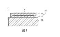
圖1是關於本發明一實施形態的承載基座1的剖面圖。承載基座1是用於半導體製造裝置中的半導體製造裝置構件。承載基座1從圖1的下側支撐大致圓盤狀的半導體基板9(以下,簡稱為「基板9」)。在以下的說明中,將圖1中的上側及下側簡稱為「上側」及「下側」。此外,將圖1中的上下方向簡稱為「上下方向」。圖1中的上下方向與承載基座1設置在半導體製造裝置中時實際的上下方向不必一致。FIG. 1 is a cross-sectional view of a
承載基座1具備本體部21、底座部22、電極23。本體部21是以陶瓷為主材料的大致板狀(例如,大致圓盤狀)的基材。本體部21的上側的主表面(即,上表面)上載置有基板9。底座部22是在平視時比本體部21大的大致板狀(例如,大致圓盤狀)的構件。本體部21安裝在底座部22上。在圖1所示的例子中,電極23配置(即,嵌入)於本體部21的內部。電極23例如是在平視時描繪成預定圖案的大致帶狀的構件。電極23較佳地藉由具有相對高熔點的材料形成。本體部21和電極23是藉由多數的材料形成的複合燒結體。在以下的說明中,將本體部21和電極23統稱為「複合燒結體20」。關於本體部21和電極23的材料於後續說明。其中,電極23的形狀可以以各種方式改變。此外,電極23可以設置在本體部21的表面上。The
在圖1所示的例子中,承載基座1是經由向電極23施加直流電壓而產生的熱量,藉此加熱基板9的加熱器。即,電極23是加熱基板9的電阻發熱體。在承載基座1中,除了電極23之外,利用庫侖力或約翰遜-拉貝克(Johnsen-Rahbek)力對基板9進行靜電吸引的卡盤用電極,可以設置在本體部21內部。或者,電極23可利用作卡盤用電極。In the example shown in FIG. 1 , the
本體部21例如由作為主材料的氧化鋁(Al2O3)形成。在本體部21中,可以向Al2O3添加如氧化鎂(MgO)及/或鎂鋁尖晶石(MgAl2O4)等的添加材料。在本體部21中,作為主材料的Al2O3的含量,例如為95質量%以上且100質量%以下,較佳為99質量%以上且100質量%以下。本體部21中Al2O3的含量,根據所需本體部21的材料特性進行調整。其中,本體部21的主材料不限於Al2O3,也可以是其他的陶瓷。The
電極23包含鎢(W)和氧化鋯(ZrO2)。在本實施形態中,電極23實質上僅由W和ZrO2形成,並且實質上不包含W和ZrO2以外的物質。換句話說,在本實施形態中,電極23中的W和ZrO2的總含量為100體積%。The
電極23中的W和ZrO2的含量,以使電極23和本體部21的熱膨脹係數的差實質上接近0的方式進行調整。此外,在電極23中,藉由X射線繞射法(XRD)獲得的W和ZrO2的主峰的強度比(以下也稱為「W-ZrO2峰值比」),例如為0.90以上且未滿0.96,並且以使電極23和本體部21的熱膨脹係數的差實質上接近0的方式進行調整。W-ZrO2峰值比是將W的主峰強度除以W的主峰強度與ZrO2的主峰強度的總和而算出的值。The contents of W and ZrO2 in the
W的熱膨脹係數(也稱為熱膨脹率)在40℃以上且1000℃以下的範圍內為5.3ppm/℃(即ppm/K)。以下說明中的熱膨脹係數,在沒有記載溫度條件的情況下,是指40℃以上且1000℃以下的範圍內的熱膨脹係數。ZrO2的熱膨脹係數為10.5ppm/℃。Al2O3的熱膨脹係數為8.0ppm/℃。本體部21的熱膨脹係數根據添加到主材料Al2O3中的添加材料的種類和比例而變化,例如為8.1ppm/℃~8.3ppm/℃。The thermal expansion coefficient (also referred to as thermal expansion coefficient) of W is 5.3 ppm/°C (ie, ppm/K) in the range of 40° C. or higher and 1000° C. or lower. The thermal expansion coefficient in the following description refers to the thermal expansion coefficient in the range of 40° C. or higher and 1000° C. or lower, unless temperature conditions are described. The thermal expansion coefficient of ZrO2 is 10.5 ppm/°C. The thermal expansion coefficient of Al2 O3 is 8.0 ppm/°C. The thermal expansion coefficient of the
電極23中所包含的W的熱膨脹係數低於本體部21的熱膨脹係數。電極23中所包含的ZrO2的熱膨脹係數高於本體部21的熱膨脹係數。40℃以上且1000℃以下的範圍內的電極23與本體部21的熱膨脹係數的差的絕對值(以下,也稱為「CTE差」),例如為0.5ppm/℃以下,較佳為0.2ppm/℃以下。CTE差的下限沒有特別限定,可為0.0ppm/℃以上。The thermal expansion coefficient of W contained in the
電極23的室溫電阻率例如為3.5×10⁻⁵Ω.cm以下,較佳為3.0×10⁻⁵Ω.cm以下。此電阻率的下限沒有特別限定,例如為1.0×10⁻⁵Ω.cm以上。The room temperature resistivity of the
電極23如後續所述,是藉由與本體部21一起、或與本體部21分別燒成而形成的燒結體。燒成溫度例如是1500℃以上的高溫。其中,W的熔點為3410℃,ZrO2的熔點為2715℃。W的燒結粒徑例如為0.7μm以上且3.0μm以下,較佳為1.0μm以上且2.0μm以下。ZrO2的燒結粒徑例如為0.7μm以上且3.0μm以下,較佳為1.0μm以上且2.0μm以下。ZrO2的燒結粒徑與W的燒結粒徑的差的絕對值(以下,簡稱為「燒結粒徑差」),例如為0.5μm以下,較佳為0.25μm以下。燒結粒徑差的下限沒有特別限定,例如為0.0μm以上。W和ZrO2的燒結粒徑可以藉由使用SEM(掃描型電子顯微鏡)等觀察微結構而求出。The
圖2是後續所述實施例10的複合燒結體20的剖面的SEM圖像。圖2中的上下方向的中央部的發白區域對應於電極23。並且,電極23的下側的黑色帶狀的區域對應於本體部21的第一構件,電極23的上側的黑色帶狀的區域對應於本體部21的第二構件。在對應於電極23的區域中,最淺色的白色的區域是W,比W更深色的灰色的區域是ZrO2。在複合燒結體20中,如上所述,藉由減小電極23中燒結粒徑差,使電極23中的W和ZrO2的分散的均勻性提高。FIG. 2 is a SEM image of a cross section of the composite
接著參照圖3,同時對關於承載基座1的本體部21和電極23(即,複合燒結體20)的製造方法的一例進行說明。在此例中,製作本體部21的下半部分的大致圓盤狀的部分(以下稱為「第一構件」),與上半部分的大致圓盤狀部分(以下稱為「第二構件」),藉由將電極23的材料夾在第一構件和第二構件之間進行燒成,製造本體部21和電極23。Next, with reference to FIG. 3 , an example of a method of manufacturing the
在此製造方法中,首先,準備本體部21的第一構件和第二構件(步驟S11)。在步驟S11中準備的第一構件和第二構件,可以是成形體、煅燒體和燒結體的任一的狀態。在步驟S11中,首先,使本體部21(即第一構件和第二構件)的原料粉末成為預定的組成的方式進行秤量,將此原料粉末濕式混合,然後藉由單軸加壓成形等,成形為預定形狀的成形體。In this manufacturing method, first, the first member and the second member of the
在步驟S11中,作為Al2O3原料,例如,使用市售的高純度微粒粉末。並且,當本體部21中含有MgO時,作為MgO原料,例如,使用市售的高純度微粒粉末。當本體部21包含MgAl2O4時,例如,將上述的市售的MgO粉末和市售的Al2O3的高純度微粒粉末進行加熱合成,作為MgAl2O4原料而使用。或者,作為MgAl2O4原料,可以使用市售的MgAl2O4的高純度微粒粉末。Al2O3原料、MgO原料和MgAl2O4原料的純度與平均粒徑等適當決定。In step S11, as the Al2 O3 raw material, for example, a commercially available high-purity fine particle powder is used. In addition, when MgO is contained in the
在步驟S11中,原料粉末的混合條件(例如,混合時間、溶劑種類等)適當決定。作為此溶劑,例如,可以使用有機溶劑或離子交換水。並且,在步驟S11中,可以藉由乾式混合來混合原料粉末。In step S11, the mixing conditions of the raw material powder (for example, mixing time, type of solvent, etc.) are appropriately determined. As this solvent, for example, an organic solvent or ion-exchanged water can be used. In addition, in step S11, the raw material powder may be mixed by dry mixing.
在步驟S11中,成形體的成形條件(例如,被施加的壓力等)適當決定。當成形體的形狀為板狀時,可以藉由將原料粉末填充到熱壓模具等使成形體進行成形。此成形體的成形只要可以保持形狀,可以藉由各種其他方法進行。例如,可以將濕式混合後的漿料,保持具有流動性的狀態注入模具後除去溶劑成分,成為預定形狀的成形體。或者,可以藉由利用刮刀等的帶成形法,形成預定量的帶成形體。In step S11, the molding conditions (for example, applied pressure, etc.) of the molded body are appropriately determined. When the shape of the formed body is a plate shape, the formed body can be formed by filling the raw material powder in a hot press die or the like. The molding of this molded body can be performed by various other methods as long as the shape can be maintained. For example, the wet-mixed slurry can be poured into a mold while maintaining fluidity, and the solvent component can be removed to obtain a molded body of a predetermined shape. Alternatively, a predetermined amount of a belt formed body can be formed by a belt forming method using a doctor blade or the like.
在步驟S11中,當準備第一構件及/或第二構件的煅燒體或燒結體時,將藉由上述的方法形成的成形體經由熱壓法等進行燒成,形成煅燒體(即,煅燒結體)或燒結體。此成形體的燒成時的燒成條件(例如壓製壓力、燒成溫度、燒成時間等)適當決定。此外,此成形體的燒成也可以藉由熱壓法以外的方法進行。In step S11, when the calcined body or sintered body of the first member and/or the second member is prepared, the formed body formed by the above-mentioned method is fired by a hot pressing method or the like to form a calcined body (that is, a calcined body). body) or sintered body. The firing conditions (for example, pressing pressure, firing temperature, firing time, etc.) at the time of firing the compact are appropriately determined. In addition, the firing of this compact may be performed by a method other than the hot pressing method.
接著,使電極23的原料粉末成為預定的組成的方式進行秤量,將此原料粉末混合後,與溶劑和黏合劑等混煉,生成作為電極23的前驅物的電極糊(步驟S12)。在步驟S12中,作為W原料和ZrO2原料,例如,使用市售的高純度微粒粉末。W原料和ZrO2原料的純度和平均粒徑等適當決定。W原料和ZrO2原料的平均粒徑,例如,未滿1μm。Next, the raw material powder of the
上述的電極23的原料粉末的混合,例如,藉由濕式混合來進行。原料粉末的混合條件(例如,混合時間、溶劑種類等)適當決定。作為此溶劑,例如,可以使用有機溶劑或離子交換水。其中,在步驟S12中,可以藉由乾式混合來混合原料粉末。在步驟S12中,與原料粉末一起混煉的上述溶劑(例如,有機溶劑)和黏合劑的種類適當決定。其中,步驟S12可以在步驟S11之前進行、或與步驟S11同時進行。The above-mentioned mixing of the raw material powders for the
步驟S12所生成的電極糊在步驟S11所形成的第一構件的上表面上,藉由網版印刷等以賦予其預定的形狀(步驟S13)。步驟S13中將電極糊賦予至成形體的第一構件上時,第一構件例如是帶成形體。其中,在步驟S13中,電極糊的塗佈可以藉由網版印刷以外的方法進行。當第一構件是成形體或煅燒體時,準確地說,將電極糊賦予到第一構件的前驅物的上表面。然後,將電極糊在空氣中等乾燥預定時間(例如,1小時)之後,在第一構件和電極糊的上方,將第二構件積層以形成積層體(步驟S14)。The electrode paste produced in step S12 is given a predetermined shape by screen printing or the like on the upper surface of the first member formed in step S11 (step S13 ). When the electrode paste is applied to the first member of the molded body in step S13, the first member is, for example, a tape molded body. Here, in step S13, the coating of the electrode paste may be performed by a method other than screen printing. When the first member is a formed body or a calcined body, to be precise, the electrode paste is applied to the upper surface of the precursor of the first member. Then, after the electrode paste is dried in air or the like for a predetermined time (eg, 1 hour), over the first member and the electrode paste, the second member is laminated to form a laminated body (step S14 ).
其中,複合燒結體20的製造中,代替上述的步驟S13~S14,將步驟S12所生成的電極糊單體燒成而形成電極23,此電極23可以配置在第一構件的上表面上,第二構件可以積層在第一構件和電極23上。Among them, in the production of the composite
之後,在步驟S14中所形成的積層體,藉由熱壓法等燒成,藉此使第一構件和第二構件一體化,形成本體部21和電極23(即,複合燒結體20)(步驟S15)。步驟S15中的燒成條件(例如,壓製壓力、燒成溫度、燒成時間等)適當決定。步驟S15中的燒成溫度(即,煅燒成時的最高溫度),例如為1550℃以上且1650℃以下。步驟S15中的積層體的燒成可以藉由熱壓法以外的方法進行。After that, the layered body formed in step S14 is fired by hot pressing or the like, whereby the first member and the second member are integrated to form the
接著,參照表1~表3,同時對本發明的複合燒結體20(即,本體部21和電極23)的實施例1~實施例13,以及為了與複合燒結體20進行比較的比較例1~比較例4的複合燒結體進行說明。實施例1~實施例13中,相對於電極23含有W和ZrO2,比較例1~比較例4中,電極23不含ZrO2,比較例1~比較例2中,電極23也不含W。Next, with reference to Tables 1 to 3, Examples 1 to 13 of the composite sintered body 20 (ie, the


在實施例1~實施例13和比較例1~比較例4中,本體部21和電極23的製造是藉由上述的步驟S11~步驟S15來進行。在實施例1~實施例13和比較例1~比較例4中,步驟S11中使用MgO作為Al2O3的添加劑。作為Al2O3原料,使用市售的Al2O3的高純度微粒粉末(純度99.99%以上,平均粒徑0.5μm)。此外,作為MgO原料,使用市售的MgO的高純度微粒粉末(純度99.9%以上、平均粒徑1μm以下)。In Examples 1 to 13 and Comparative Examples 1 to 4, the production of the
在實施例1~實施例13和比較例1~比較例4中,步驟S11中的原料粉末的濕式混合是藉由使用氧化鋁球和圓筒型塑膠罐(polypot)的球磨機來進行。混合時間為20小時,使用的溶劑為有機溶劑。將藉由濕式混合所生成的漿料,進行乾燥後過篩,藉此得到本體部21的原料粉末。此外,步驟S11中成形體的成形,是藉由在單軸加壓成形用的模具中填充原料粉末來進行。此單軸加壓成形時的壓力為100kgf/cm2。得到的成形體為直徑50mm、厚度10mm的大致圓盤狀。其中,在實施例1~實施例13和比較例1~比較例4中,製作比實際的複合燒結體20小的試驗體並使用之。In Examples 1 to 13 and Comparative Examples 1 to 4, the wet mixing of the raw material powder in step S11 was performed by a ball mill using alumina balls and a cylindrical polypot. The mixing time was 20 hours, and the solvent used was an organic solvent. The raw material powder of the
在實施例1~實施例13和比較例1~比較例4中,步驟S12中,作為W原料和ZrO2原料,使用市售的W的高純度微粒粉末(純度99.9%以上,平均粒徑0.8μm),以及,使用ZrO2的高純度微粒粉末(純度99%以上,平均粒徑0.4μm)。In Examples 1 to 13 and Comparative Examples 1 to 4, in step S12, as the W raw material and ZrO2 raw material, commercially available high-purity fine particle powder of W (purity 99.9% or more, average particle diameter 0.8 μm), and high-purity particulate powder of ZrO2 (purity 99% or more, average particle size 0.4 μm).
在實施例1~實施例13和比較例1~比較例4中,步驟S12中的原料粉末的濕式混合是藉由使用氧化鋁球和圓筒型塑膠罐的球磨機來進行。混合時間為20小時,使用的溶劑為有機溶劑。將藉由濕式混合所生成的漿料,進行乾燥後過篩,藉此得到電極23的原料粉末。另外,在生成電極糊時,作為與此原料粉末混煉的溶劑和黏合劑,使用丁基卡必醇和聚甲基丙烯酸正丁酯。In Examples 1 to 13 and Comparative Examples 1 to 4, the wet mixing of the raw material powder in step S12 was performed by a ball mill using alumina balls and a cylindrical plastic tank. The mixing time was 20 hours, and the solvent used was an organic solvent. The raw material powder of the
在實施例1~實施例13和比較例1~比較例4中,步驟S13中的電極糊的塗佈是藉由網版印刷進行。塗佈在第一構件上的電極糊的形狀是寬5mm、長15mm的大致矩形。電極糊的厚度為60μm~70μm。In Examples 1 to 13 and Comparative Examples 1 to 4, the application of the electrode paste in step S13 was performed by screen printing. The shape of the electrode paste applied on the first member was a substantially rectangular shape with a width of 5 mm and a length of 15 mm. The thickness of the electrode paste is 60 μm to 70 μm.
在實施例1~實施例13和比較例1~比較例4中,步驟S13、S14中,作為第一構件和第二構件,使用成形體、煅燒體或燒結體的任一者。當作為第一構件或第二構件使用成形體時,使用在上述的步驟S11所得到的成形體。In Examples 1 to 13 and Comparative Examples 1 to 4, in Steps S13 and S14, any one of a molded body, a calcined body, or a sintered body was used as the first member and the second member. When the molded body is used as the first member or the second member, the molded body obtained in the above-mentioned step S11 is used.
當作為第一構件或第二構件使用煅燒體時,通過與前述成形體相同的方法製作成形體,並通過熱處理製作。燒成溫度(即,熱處理時的最高溫度)為800℃以上且1000℃以下。然後,將得到的煅燒體加工成直徑50mm、厚度5mm的大致圓盤狀。其中,煅燒體通過在原料粉末中添加有機黏合劑等的成形助劑,對已保持形狀的成形品加熱處理等製作方法,適當採用既存的方法即可,其製作條件不限於上述。When the calcined body is used as the first member or the second member, the formed body is produced by the same method as the above-mentioned formed body, and is produced by heat treatment. The firing temperature (that is, the maximum temperature during heat treatment) is 800° C. or higher and 1000° C. or lower. Then, the obtained calcined body was processed into a substantially disk shape having a diameter of 50 mm and a thickness of 5 mm. Among them, the calcined body may be prepared by adding a molding aid such as an organic binder to the raw material powder, and heat-treating the shape-retained molded product. Existing methods may be appropriately used, and the production conditions are not limited to the above.
當作為第一構件或第二構件使用燒結體時,藉由熱壓法進行成形體的燒成。具體來說,將上述的成形體裝入熱壓用的石墨模具中,設置在熱壓爐中進行燒成。煅燒成時的壓製壓力為200kgf/cm2。燒成溫度(即,煅燒成時的最高溫度)為1550℃以上且1650℃以下。燒成時間為8小時。升溫速度和降溫速度為300℃/h。當升溫至1000℃時,將燒成環境進行抽真空,然後引入氮氣。引入氮氣後的氣壓維持在約1.5atm(約0.152MPa)。當降溫時,溫度控制在1400℃停止並冷卻爐子。然後,將得到的燒結體加工成直徑50mm、厚度5mm的大致圓盤狀。When a sintered body is used as the first member or the second member, the formed body is fired by a hot pressing method. Specifically, the above-mentioned molded body is put into a graphite mold for hot pressing, and is set in a hot pressing furnace to be fired. The pressing pressure during calcination was 200 kgf/cm2 . The firing temperature (that is, the highest temperature during firing) is 1550°C or higher and 1650°C or lower. The firing time was 8 hours. The heating rate and cooling rate were 300°C/h. When the temperature was raised to 1000°C, the firing environment was evacuated, and then nitrogen gas was introduced. The gas pressure after introduction of nitrogen gas was maintained at about 1.5 atm (about 0.152 MPa). When cooling down, the temperature was controlled at 1400°C to stop and cool down the furnace. Then, the obtained sintered body was processed into a substantially disk shape with a diameter of 50 mm and a thickness of 5 mm.
在實施例1~實施例13和比較例1~比較例4中,步驟S15中積層後的燒成是藉由熱壓法進行。具體來說,將上述的積層體裝入熱壓用的石墨模具中,設置在熱壓爐中進行燒成。燒成時的壓製壓力為200kgf/cm2。燒成溫度(即,燒成時的最高溫度)為1550℃以上且1650℃以下。燒成時間為4小時~8小時。升溫速度和降溫速度為300℃/h。燒成環境是氮氣環境。In Examples 1 to 13 and Comparative Examples 1 to 4, the firing after lamination in step S15 was performed by a hot pressing method. Specifically, the above-mentioned layered body is put into a graphite mold for hot pressing, and is set in a hot pressing furnace to be fired. The pressing pressure during firing was 200 kgf/cm2 . The firing temperature (that is, the maximum temperature during firing) is 1550°C or higher and 1650°C or lower. The firing time is 4 hours to 8 hours. The heating rate and cooling rate were 300°C/h. The firing environment is a nitrogen atmosphere.
在表1~表3中,基材(即,本體部21的第一構件和第二構件)的熱膨脹係數是使用從本體部21所切出的燒結體試樣,藉由根據JIS-R1618的方法在40℃~1000℃的範圍內測量。並且,實施例1~實施例13的電極23的熱膨脹係數,是基於W和ZrO2各自單體的熱膨脹係數、以及電極23中W和ZrO2的含量來求出。具體來說,W單體的熱膨脹係數與電極23中W的含量(體積%)的乘積,以及ZrO2單體的熱膨脹係數與電極23中ZrO2的含量(體積%)的乘積的總和作為電極23的熱膨脹係數。W和ZrO2各自單體的熱膨脹係數是將步驟S12中所使用市售的W粉末和ZrO2粉末,通過與步驟S11相同的條件下熱壓燒成而製作的基體材料,使用此基體材料並藉由根據JIS-R1618的方法在40℃~1000℃的範圍內測量。相同方法也適用於比較例1~比較例4。CTE差如上所述,是電極23的熱膨脹係數與本體部21的熱膨脹係數的差的絕對值。In Tables 1 to 3, the thermal expansion coefficients of the base materials (ie, the first member and the second member of the main body portion 21 ) were obtained by using a sintered body sample cut out from the
電極23中的W-ZrO2峰值比是藉由上述的XRD來測量W和ZrO2的主峰的強度比。W-ZrO2峰值比是將W的主峰(110)面的強度設為I1,將ZrO2的主峰(111)面的強度設為I2,由I1/(I1+I2)算出。此外,藉由XRD的測量中,除去第二構件並且露出位於第一構件上的電極23以進行測量。作為X射線繞射裝置,使用密管型X射線繞射裝置(Bruker AXS Co.,Ltd.製的D8 ADVANCE)。測量條件為CuKα、40kV、40mA、2θ=10~70∘,步距為0.002∘。The W-ZrO2 peak ratio in the
電極23中W的燒結粒徑,是藉由使用SEM觀察微結構來求出。具體來說,將試驗片的一個表面拋光加工成鏡面狀,並將電極23的拋光面使用SEM觀察。然後算出平均直徑,此平均直徑是預定數量(例如,數十個)的燒結粒子的各自的長軸與短軸的平均值。將此預定數量的燒結粒子的平均直徑的算術平均值定義為W的燒結粒徑。關於電極23中ZrO2的燒結粒徑也適用相同方式。The sintered grain size of W in the
電極23的電阻率由下述方式求出。首先,從步驟S15中所形成的複合燒結體20切出寬度、長度和厚度各自為9mm的大致長方體狀的試驗片。試驗片是以寬度5mm、長度9mm的電極23可內置於中央部的方式切出。試驗片的兩個端面上露出寬度5mm的電極23。電極23的剖面積S(cm2)是藉由光學顯微鏡測量試驗片的端面上的電極23的寬度和長度來求出。此外,藉由卡尺測量電極23暴露在試驗片的兩個端面之間的距離,作為電極23的長度L(cm)。電阻測量用的電路是通過在電極23的兩端面塗佈導電膏並連接導線而構成。然後,在大氣中的室溫下,在0mA~150mA的範圍內向電極23施加微小電流I(mA),測量此時產生的微小電壓值V(mV),電極23的電阻R(Ω)藉由R=V/I求出。然後,電極23的電阻率ρ(Ω.cm)藉由ρ=R×S/L求出。The resistivity of the
電極23的組成由下述方式求出。首先,去除試驗片的上半部或下半部,使電極23的上表面或下表面露出,對露出的電極23進行拋光。然後,在電極23的拋光面上,藉由上述的X射線繞射裝置在上述測量條件下鑑定結晶相。The composition of the
在實施例1~實施例13和比較例1~比較例4中,本體部21的主材料為Al2O3,添加劑為MgO。此外,如上所述,在實施例1~實施例13中,電極23是藉由W和ZrO2而形成。換句話說,實施例1~實施例13中,電極23中W和ZrO2的總含量為100體積%。另一方面,在比較例1中,電極23僅由碳化鎢(WC)形成,並且不含W和ZrO2。在比較例2中,電極23由WC和Al2O3形成,並且不含W和ZrO2。在比較例3中,電極23僅由W形成,並且不含ZrO2。在比較例4中,電極23由W和Al2O3形成,並且不含ZrO2。In Examples 1 to 13 and Comparative Examples 1 to 4, the main material of the
在實施例1中,步驟S13中被賦予電極糊的本體部21的第一構件是燒結體。並且,步驟S14中積層在第一構件上的第二構件是成形體。本體部21的MgO的含量為0.025質量%,本體部21的熱膨脹係數為8.1ppm/℃。其中,本體部21的MgO以外的其餘部分是Al2O3(其他的實施例與比較例也適用相同方式)。電極23中W的含量為46.2體積%,ZrO2的含量為53.8體積%。電極23的熱膨脹係數為8.1ppm/℃。複合燒結體20的燒成溫度(即,燒成時的最高溫度)為1600℃。In Example 1, the first member of the
在實施例1中,CTE差(即,在40℃以上且1000℃以下的範圍內,電極23和本體部21的熱膨脹係數的差的絕對值)為0.0ppm/℃。W-ZrO2峰值比為0.94。W和ZrO2的燒結粒徑各自為1.17μm和1.27μm,燒結粒徑差(即,ZrO2的燒結粒徑與W的燒結粒徑的差的絕對值)為0.10μm。電極23的電阻率為2.9×10-5Ω.cm。電極23的組成是W和ZrO2。In Example 1, the CTE difference (ie, the absolute value of the difference in thermal expansion coefficient between the
在實施例1中,由於CTE差小到0.5ppm/℃以下,沒有產生由本體部21和電極23的熱膨脹係數的差所引起的本體部21的裂紋、電極23的剝離。並且,電極23的電阻率小到3.5×10-5Ω.cm以下。W-ZrO2峰值比為0.90以上且未滿0.96的合適範圍內,藉此,可以合適地兼顧上述的熱膨脹係數的差的減少與抑制電阻率的增大。ZrO2的燒結粒徑為0.7μm以上且3.0μm以下的合適範圍內,燒結粒徑差(即,W的燒結粒徑與ZrO2的燒結粒徑的差)小到0.5μm以下。因此,電極23中實現了W和ZrO2的大致均勻的分散。In Example 1, since the CTE difference was as small as 0.5 ppm/°C or less, cracks in the
在實施例2中,本體部21中MgO的含量為1.0質量%,本體部21的熱膨脹係數為8.2ppm/℃。電極23中W的含量為44.2體積%,ZrO2的含量為55.8體積%。電極23的熱膨脹係數為8.2ppm/℃。其他條件與實施例1相同。In Example 2, the content of MgO in the
在實施例2中,CTE差為0.0ppm/℃。W-ZrO2峰值比為0.93。W和ZrO2的燒結粒徑各自為1.15μm和1.32μm,燒結粒徑差為0.17μm。電極23的電阻率為3.0×10-5Ω.cm。電極23的組成是W和ZrO2。In Example 2, the CTE difference was 0.0 ppm/°C. The W-ZrO2 peak ratio is 0.93. The sintered grain sizes of W and ZrO2 were 1.15 μm and 1.32 μm, respectively, and the difference in sintered grain sizes was 0.17 μm. The resistivity of the
在實施例2中,由於CTE差小,沒有產生由本體部21和電極23的熱膨脹係數的差所引起的本體部21的裂紋、電極23的剝離。並且,電極23的電阻率小。進一步地,由於ZrO2的燒結粒徑在合適的範圍內,並且燒結粒徑差較小,在電極23中實現了W和ZrO2的大致均勻的分散。In Example 2, since the difference in CTE was small, cracks in the
在實施例3中,本體部21中MgO的含量為5.0質量%,本體部21的熱膨脹係數為8.3ppm/℃。電極23中W的含量為42.3體積%,ZrO2的含量為57.7體積%。電極23的熱膨脹係數為8.3ppm/℃。其他條件與實施例1相同。In Example 3, the content of MgO in the
在實施例3中,CTE差為0.0ppm/℃。W-ZrO2峰值比為0.91。W和ZrO2的燒結粒徑各自為1.14μm和1.36μm,燒結粒徑差為0.22μm。電極23的電阻率為3.2×10-5Ω.cm。電極23的組成是W和ZrO2。In Example 3, the CTE difference was 0.0 ppm/°C. The W-ZrO2 peak ratio is 0.91. The sintered grain sizes of W and ZrO2 were 1.14 μm and 1.36 μm, respectively, and the difference in sintered grain sizes was 0.22 μm. The resistivity of the
在實施例3中,由於CTE差小,沒有產生由本體部21和電極23的熱膨脹係數的差所引起的本體部21的裂紋、電極23的剝離。並且,電極23的電阻率小。進一步地,由於ZrO2的燒結粒徑在合適的範圍內,並且燒結粒徑差較小,在電極23中實現了W和ZrO2的大致均勻的分散。In Example 3, since the difference in CTE was small, cracks in the
注目於實施例1~實施例3,即使本體部21的熱膨脹係數在上述範圍(即,8.1ppm/℃~8.3ppm/℃)內改變,CTE差仍可為0.0ppm/℃,並可防止本體部21產生裂紋、電極23的剝離。並且,可抑制電極23的電阻率的增大。Note that in Examples 1 to 3, even if the thermal expansion coefficient of the
在實施例4中,電極23中W的含量為55.8體積%,ZrO2的含量為44.2體積%。電極23的熱膨脹係數為7.6ppm/℃。其他條件與實施例1相同。In Example 4, the content of W in the
在實施例4中,CTE差為0.5ppm/℃。W-ZrO2峰值比為0.96。W和ZrO2的燒結粒徑各自為1.20μm和1.11μm,燒結粒徑差為0.09μm。電極23的電阻率為2.0×10-5Ω.cm。電極23的組成是W和ZrO2。In Example 4, the CTE difference was 0.5 ppm/°C. The W-ZrO2 peak ratio is 0.96. The sintered grain sizes of W and ZrO2 were 1.20 μm and 1.11 μm, respectively, and the difference in sintered grain sizes was 0.09 μm. The resistivity of the
在實施例4中,由於CTE差小(即,0.5ppm/℃以下),沒有產生由本體部21和電極23的熱膨脹係數的差所引起的本體部21的裂紋、電極23的剝離。並且,電極23的電阻率小。進一步地,由於ZrO2的燒結粒徑在合適的範圍內,並且燒結粒徑差較小,在電極23中實現了W和ZrO2的大致均勻的分散。In Example 4, since the CTE difference was small (ie, 0.5 ppm/°C or less), cracks in the
在實施例5中,電極23中W的含量為51.9體積%,ZrO2的含量為48.1體積%。電極23的熱膨脹係數為7.8ppm/℃。其他條件與實施例1相同。In Example 5, the content of W in the
在實施例5中,CTE差為0.3ppm/℃。W-ZrO2峰值比為0.95。W和ZrO2的燒結粒徑各自為1.19μm和1.14μm,燒結粒徑差為0.05μm。電極23的電阻率為2.5×10-5Ω.cm。電極23的組成是W和ZrO2。In Example 5, the CTE difference was 0.3 ppm/°C. The W-ZrO2 peak ratio is 0.95. The sintered particle sizes of W and ZrO2 were 1.19 μm and 1.14 μm, respectively, and the difference in sintered particle sizes was 0.05 μm. The resistivity of the
在實施例5中,由於CTE差小,沒有產生由本體部21和電極23的熱膨脹係數的差所引起的本體部21的裂紋、電極23的剝離。並且,電極23的電阻率小。進一步地,由於ZrO2的燒結粒徑在合適的範圍內,並且燒結粒徑差較小,在電極23中實現了W和ZrO2的大致均勻的分散。In Example 5, since the difference in CTE was small, cracks in the
在實施例6中,電極23中W的含量為48.1體積%,ZrO2的含量為51.9體積%。電極23的熱膨脹係數為8.0ppm/℃。其他條件與實施例1相同。In Example 6, the content of W in the
在實施例6中,CTE差為0.1ppm/℃。W-ZrO2峰值比為0.95。W和ZrO2的燒結粒徑各自為1.18μm和1.22μm,燒結粒徑差為0.04μm。電極23的電阻率為2.8×10-5Ω.cm。電極23的組成是W和ZrO2。In Example 6, the CTE difference was 0.1 ppm/°C. The W-ZrO2 peak ratio is 0.95. The sintered particle sizes of W and ZrO2 were 1.18 μm and 1.22 μm, respectively, and the difference in sintered particle sizes was 0.04 μm. The resistivity of the
在實施例6中,由於CTE差小,沒有產生由本體部21和電極23的熱膨脹係數的差所引起的本體部21的裂紋、電極23的剝離。並且,電極23的電阻率小。進一步地,由於ZrO2的燒結粒徑在合適的範圍內,並且燒結粒徑差較小,在電極23中實現了W和ZrO2的大致均勻的分散。In Example 6, since the difference in CTE was small, cracks in the
在實施例7中,電極23中W的含量為44.2體積%,ZrO2的含量為55.8體積%。電極23的熱膨脹係數為8.2ppm/℃。其他條件與實施例1相同。In Example 7, the content of W in the
在實施例7中,CTE差為0.1ppm/℃。W-ZrO2峰值比為0.93。W和ZrO2的燒結粒徑各自為1.16μm和1.30μm,燒結粒徑差為0.14μm。電極23的電阻率為3.1×10-5Ω.cm。電極23的組成是W和ZrO2。In Example 7, the CTE difference was 0.1 ppm/°C. The W-ZrO2 peak ratio is 0.93. The sintered grain sizes of W and ZrO2 were 1.16 μm and 1.30 μm, respectively, and the difference in sintered grain sizes was 0.14 μm. The resistivity of the
在實施例7中,由於CTE差小,沒有產生由本體部21和電極23的熱膨脹係數的差所引起的本體部21的裂紋、電極23的剝離。並且,電極23的電阻率小。進一步地,由於ZrO2的燒結粒徑在合適的範圍內,並且燒結粒徑差較小,在電極23中實現了W和ZrO2的大致均勻的分散。In Example 7, since the difference in CTE was small, cracks in the
在實施例8中,電極23中W的含量為40.4體積%,ZrO2的含量為59.6體積%。電極23的熱膨脹係數為8.4ppm/℃。其他條件與實施例1相同。In Example 8, the content of W in the
在實施例8中,CTE差為0.3ppm/℃。W-ZrO2峰值比為0.91。W和ZrO2的燒結粒徑各自為1.14μm和1.35μm,燒結粒徑差為0.21μm。電極23的電阻率為3.3×10-5Ω.cm。電極23的組成是W和ZrO2。In Example 8, the CTE difference was 0.3 ppm/°C. The W-ZrO2 peak ratio is 0.91. The sintered grain sizes of W and ZrO2 were 1.14 μm and 1.35 μm, respectively, and the difference in sintered grain sizes was 0.21 μm. The resistivity of the
在實施例8中,由於CTE差小,沒有產生由本體部21和電極23的熱膨脹係數的差所引起的本體部21的裂紋、電極23的剝離。並且,電極23的電阻率小。進一步地,由於ZrO2的燒結粒徑在合適的範圍內,並且燒結粒徑差較小,在電極23中實現了W和ZrO2的大致均勻的分散。In Example 8, since the difference in CTE was small, cracks in the
在實施例9中,電極23中W的含量為36.5體積%,ZrO2的含量為63.5體積%。電極23的熱膨脹係數為8.6ppm/℃。其他條件與實施例1相同。In Example 9, the content of W in the
在實施例9中,CTE差為0.5ppm/℃。W-ZrO2峰值比為0.90。W和ZrO2的燒結粒徑各自為1.13μm和1.38μm,燒結粒徑差為0.25μm。電極23的電阻率為3.5×10-5Ω.cm。電極23的組成是W和ZrO2。In Example 9, the CTE difference was 0.5 ppm/°C. The W- ZrO peak ratio is 0.90. The sintered grain sizes of W and ZrO2 were 1.13 μm and 1.38 μm, respectively, and the difference in sintered grain sizes was 0.25 μm. The resistivity of the
在實施例9中,由於CTE差小,沒有產生由本體部21和電極23的熱膨脹係數的差所引起的本體部21的裂紋、電極23的剝離。並且,電極23的電阻率小。進一步地,由於ZrO2的燒結粒徑在合適的範圍內,並且燒結粒徑差較小,在電極23中實現了W和ZrO2的大致均勻的分散。In Example 9, since the difference in CTE was small, cracks in the
注目於實施例1、實施例4~實施例9,即使電極23中W和ZrO2的含量改變,CTE差仍在上述範圍(即,0.0ppm/℃~0.5ppm/℃)內改變,並可防止本體部21產生裂紋、電極23的剝離。並且,可抑制電極23的電阻率的增大。Note that in Example 1, Example 4 to Example 9, even if the contents of W and ZrO2 in the
在實施例10中,複合燒結體20的燒成溫度為1550℃。其他條件與實施例1相同。In Example 10, the firing temperature of the composite
在實施例10中,電極23的熱膨脹係數為8.0ppm/℃,CTE差為0.1ppm/℃。W-ZrO2峰值比為0.94。W和ZrO2的燒結粒徑各自為0.94μm和0.82μm,燒結粒徑差為0.12μm。電極23的電阻率為3.0×10-5Ω.cm。電極23的組成是W和ZrO2。In Example 10, the thermal expansion coefficient of the
在實施例10中,由於CTE差小,沒有產生由本體部21和電極23的熱膨脹係數的差所引起的本體部21的裂紋、電極23的剝離。並且,電極23的電阻率小。進一步地,由於ZrO2的燒結粒徑在合適的範圍內,並且燒結粒徑差較小,在電極23中實現了W和ZrO2的大致均勻的分散。In Example 10, since the difference in CTE was small, cracks in the
在實施例11中,複合燒結體20的燒成溫度為1650℃。其他條件與實施例1相同。In Example 11, the firing temperature of the composite
在實施例11中,電極23的熱膨脹係數為8.2ppm/℃,CTE差為0.1ppm/℃。W-ZrO2峰值比為0.93。W和ZrO2的燒結粒徑各自為1.81μm和1.72μm,燒結粒徑差為0.09μm。電極23的電阻率為3.1×10-5Ω.cm。電極23的組成是W和ZrO2。In Example 11, the thermal expansion coefficient of the
在實施例11中,由於CTE差小,沒有產生由本體部21和電極23的熱膨脹係數的差所引起的本體部21的裂紋、電極23的剝離。並且,電極23的電阻率小。進一步地,由於ZrO2的燒結粒徑在合適的範圍內,並且燒結粒徑差較小,在電極23中實現了W和ZrO2的大致均勻的分散。In Example 11, since the difference in CTE was small, cracks in the
注目實施例1、實施例10~實施例11,即使複合燒結體20的燒成溫度在上述範圍(即,1550℃~1650℃)內改變,CTE差仍小到0.0ppm/℃~0.1ppm/℃,並可防止本體部21產生裂紋、電極23的剝離。並且,可抑制電極23的電阻率的增大。Note that in Example 1 and Example 10 to Example 11, even if the firing temperature of the composite
在實施例12中,在步驟S11中準備的第一構件、以及在步驟S14中積層在第一構件上的第二構件是煅燒體。其他條件與實施例1相同。In Example 12, the first member prepared in step S11 and the second member laminated on the first member in step S14 are calcined bodies. Other conditions are the same as in Example 1.
在實施例12中,CTE差為0.0ppm/℃。W-ZrO2峰值比為0.93。W和ZrO2的燒結粒徑各自為2.22μm和2.55μm,燒結粒徑差為0.33μm。電極23的電阻率為2.8×10-5Ω.cm。電極23的組成是W和ZrO2。In Example 12, the CTE difference was 0.0 ppm/°C. The W-ZrO2 peak ratio is 0.93. The sintered particle sizes of W and ZrO2 were 2.22 μm and 2.55 μm, respectively, and the difference in sintered particle sizes was 0.33 μm. The resistivity of the
在實施例12中,由於CTE差小,沒有產生由本體部21和電極23的熱膨脹係數的差所引起的本體部21的裂紋、電極23的剝離。並且,電極23的電阻率小。進一步地,由於ZrO2的燒結粒徑在合適的範圍內,並且燒結粒徑差較小,在電極23中實現了W和ZrO2的大致均勻的分散。In Example 12, since the difference in CTE was small, cracks in the
在實施例13中,在步驟S14中積層在第一構件上的第二構件是燒結體。其他條件與實施例1相同。In Example 13, the second member laminated on the first member in step S14 is a sintered body. Other conditions are the same as in Example 1.
在實施例13中,CTE差為0.0ppm/℃。W-ZrO2峰值比為0.94。W和ZrO2的燒結粒徑各自為1.15μm和1.25μm,燒結粒徑差為0.10μm。電極23的電阻率為2.9×10-5Ω.cm。電極23的組成是W和ZrO2。In Example 13, the CTE difference was 0.0 ppm/°C. The W-ZrO2 peak ratio is 0.94. The sintered grain sizes of W and ZrO2 were 1.15 μm and 1.25 μm, respectively, and the difference in sintered grain sizes was 0.10 μm. The resistivity of the
在實施例13中,由於CTE差小,沒有產生由本體部21和電極23的熱膨脹係數的差所引起的本體部21的裂紋、電極23的剝離。並且,電極23的電阻率小。進一步地,由於ZrO2的燒結粒徑在合適的範圍內,並且燒結粒徑差較小,在電極23中實現了W和ZrO2的大致均勻的分散。In Example 13, since the difference in CTE was small, cracks in the
注目於實施例1、實施例12~實施例13,即使在步驟S15中燒結前的第一構件和第二構件的狀態(即,成形體、煅燒體或燒結體)改變時,CTE差仍為0.0ppm/℃,並可防止本體部21產生裂紋、電極23的剝離。並且,可抑制電極23的電阻率的增大。Note that in Example 1, Example 12 to Example 13, even when the states of the first member and the second member before sintering in step S15 (ie, the formed body, the calcined body, or the sintered body) were changed, the difference in CTE was 0.0 ppm/°C, cracks in the
在比較例1中,如上所述,電極23僅由WC形成,並且不含W和ZrO2。電極23的熱膨脹係數為5.3ppm/℃。其他條件與實施例1相同。在比較例1中,由於CTE差大到2.8ppm/℃,會產生由本體部21和電極23的熱膨脹係數的差所引起的本體部21的裂紋、電極23的剝離。並且,電極23的組成為WC和W2C。此W2C是藉由高溫燒成使WC的一部分氧化而生成,電極23中WC和W2C的含量變動而使電極23的特性(例如,電阻率、熱膨脹係數等)具有變得不穩定的可能性。In Comparative Example 1, as described above, the
在比較例2中,如上所述,電極23由WC和Al2O3形成,並且不含W和ZrO2。電極23的熱膨脹係數為6.1ppm/℃。其他條件與實施例1相同。在比較例2中,由於CTE差大到2.0ppm/℃,會產生由本體部21和電極23的熱膨脹係數的差所引起的本體部21的裂紋、電極23的剝離。並且,電極23的組成為WC、W2C和Al2O3。因此,與比較例1相同,使電極23的特性具有變得不穩定的可能性。In Comparative Example 2, as described above, the
在比較例3中,如上所述,電極23僅由W形成,並且不含ZrO2。電極23的熱膨脹係數為5.3ppm/℃。其他條件與實施例1相同。在比較例3中,由於CTE差大到2.5ppm/℃,會產生由本體部21和電極23的熱膨脹係數的差所引起的本體部21的裂紋、電極23的剝離。並且,電極23的組成為W。In Comparative Example 3, as described above, the
在比較例4中,如上所述,電極23由W和Al2O3形成,並且不含ZrO2。電極23的熱膨脹係數為6.1ppm/℃。其他條件與實施例1相同。在比較例4中,由於CTE差大到2.0ppm/℃,會產生由本體部21和電極23的熱膨脹係數的差所引起的本體部21的裂紋、電極23的剝離。並且,電極23的組成為W和Al2O3。In Comparative Example 4, as described above, the
如同以上的說明,複合燒結體20具備:基材(上述例中的本體部21),以陶瓷作為主材料;以及電極23,配置於此基材的內部或表面。電極23包含W和ZrO2。藉此,如實施例1~實施例13所示,可以減少電極23和基材的熱膨脹係數的差。其結果為,可以抑制由電極23和基材的熱膨脹係數的差所引起的基材的裂紋、電極23的剝離。並且,在複合燒結體20中,可抑制電極23的電阻率的增大。其結果為,可以精度良好地控制由電極23產生的熱量。進一步地,由於W和ZrO2不是Ni、Co等磁性材料,即使將複合燒結體20用作靜電吸盤時,仍可抑制藉由庫侖力對基板9的吸附的阻礙。As described above, the composite
如上所述,電極23和基材的熱膨脹係數的差的絕對值,在40℃以上且1000℃以下的範圍內,較佳為0.5ppm/℃以下。藉此,可以進一步地抑制由電極23和基材的熱膨脹係數的差所引起的基材的裂紋、電極23的剝離。As described above, the absolute value of the difference between the thermal expansion coefficients of the
如上所述,電極23在室溫下的電阻率較佳為3.5×10⁻⁵Ω.cm以下。藉此,可以更加精度良好地控制由電極23產生的熱量。As mentioned above, the resistivity of the
如上所述,在電極23中,藉由X射線繞射法所獲得的W和ZrO2的主峰的強度比(即,W-ZrO2峰值比)較佳為0.90以上且未滿0.96。如此,藉由將電極23中的W和ZrO2的組成比設為合適的範圍,在合適地抑制電極23的電阻率的增大的同時,可以合適地減少電極23和基材的熱膨脹係數的差。As described above, in the
如上所述,電極23中W和ZrO2的總含量較佳為100體積%。藉此,可防止由電極23的材料的種類增加而使製造成本增大。As described above, the total content of W and ZrO2 in the
如上所述,ZrO2的燒結粒徑較佳為0.7μm以上且3.0μm以下。藉此,可以提高電極23中ZrO2的分散的均勻性。其結果為,可以實現電極23全體中,抑制電阻率的增大、以及減少與基材的熱膨脹係數差。As described above, the sintered grain size of ZrO2 is preferably 0.7 μm or more and 3.0 μm or less. Thereby, the uniformity of the dispersion of ZrO2 in the
如上所述,ZrO2的燒結粒徑與W的燒結粒徑的差的絕對值(即,燒結粒徑差)較佳為0.5μm以下。藉此,可以提高電極23中W和ZrO2的分散的均勻性。其結果為,可以實現電極23全體中,抑制電阻率的增大、以及減少與基材的熱膨脹係數差。As described above, the absolute value of the difference between the sintered grain size of ZrO2 and the sintered grain size of W (ie, the difference in sintered grain size) is preferably 0.5 μm or less. Thereby, the uniformity of the dispersion of W and ZrO2 in the
如上所述,基材的主材料為Al2O3,此基材中Al2O3的含量較佳為95質量%以上。藉此,當製造複合燒結體20時,複合燒結體20成為可以高溫燒成。因此,可以抑制燒成時W的碳化和氧化。其結果為,可以穩定電極23的特性。As described above, the main material of the base material is Al2 O3 , and the content of Al2 O3 in the base material is preferably 95% by mass or more. Thereby, when the composite
如上所述,在複合燒結體20中,在抑制電極23的電阻率的增大的同時,減少電極23和基材的熱膨脹係數的差,可以抑制基材產生裂紋、電極23的剝離。因此,複合燒結體20適用於半導體製造裝置中所使用的半導體製造裝置構件。複合燒結體20特別適用於高功率蝕刻裝置等的高輸出半導體製造裝置中所使用的半導體製造裝置構件。作為使用複合燒結體20作成的半導體製造裝置構件的合適的一例,可列舉上述的承載基座1。在承載基座1中,如上所述,本體部21為圓盤狀,並且本體部21的主表面上載置有基板9。As described above, in the composite
上述的複合燒結體20的製造方法具備:準備以陶瓷作為主材料的成形體、煅燒體或燒結體的第一構件和第二構件的步驟(步驟S11),在此第一構件上配置包含W和ZrO2的電極23或電極23的前驅物後,積層第二構件以形成積層體的步驟(步驟S13、S14)、以及將此積層體熱壓燒成的步驟(步驟S15)。藉此,與上述同樣地,可抑制由電極23和基材的熱膨脹係數的差所引起的基材的裂紋、電極23的剝離。The above-described method for producing the composite
如上所述,步驟S15終了後的電極23與第一構件和第二構件的熱膨脹係數的差的絕對值,在40℃以上且1000℃以下的範圍內,較佳為0.5ppm/℃以下。藉此,可進一步地抑制由電極23和基材的熱膨脹係數的差所引起的基材的裂紋、電極23的剝離。As described above, the absolute value of the difference between the thermal expansion coefficients of the
如上所述,步驟S15中的燒成溫度較佳為1550℃以上且1650℃以下。藉此,可抑制燒成時W的碳化和氧化。其結果為,可以穩定電極23的特性。As described above, the firing temperature in step S15 is preferably 1550°C or higher and 1650°C or lower. Thereby, carbonization and oxidation of W during firing can be suppressed. As a result, the characteristics of the
上述的複合燒結體20、半導體製造裝置構件、以及複合燒結體20的製造方法可以進行各種變更。Various modifications can be made to the above-described composite
例如,複合燒結體20的CTE差可以大於0.5ppm/℃。For example, the CTE difference of the composite
電極23在室溫下的電阻率可以高於3.5×10⁻⁵Ω.cm。The resistivity of the
電極23中,W-ZrO2峰值比可以未滿0.90,也可以0.96以上。In the
電極23的固體物質中的W和ZrO2的總含量可以未滿100體積%。The total content of W and ZrO2 in the solid matter of the
電極23中,ZrO2的燒結粒徑可以未滿0.7μm,也可以大於3.0μm。In the
電極23中,ZrO2的燒結粒徑與W的燒結粒徑的差的絕對值(即,燒結粒徑差)可以大於0.5μm。In the
本體部21中Al2O3的含量可以未滿95質量%。並且,本體部21的主材料可以是Al2O3以外的陶瓷。The content of Al2 O3 in the
複合燒結體20的製造方法中,上述的步驟S15中的燒成溫度可以未滿1550℃,也可以溫度高於1650℃。In the manufacturing method of the composite
複合燒結體20可以藉由與上述製造方法不同的方法來製造。例如,可以省略步驟S12,且在步驟S13中,可以將電極23的原料粉末(即,電極23的前驅物)賦予在第一構件上。The composite
複合燒結體20可以用於製作除承載基座1以外的半導體製造裝置中所設置其他的半導體製造裝置構件(例如,環、噴頭等)。此外,可以藉由複合燒結體20製作除半導體製造裝置以外的裝置中所使用的構件。例如,複合燒結體20可以用於製作支撐除半導體基板以外的基板的承載基座,也可以用於製作加熱對象物的陶瓷加熱器。The composite
上述實施形態及其各種變形例中的構成只要不相互衝突,即可適當地組合。The configurations in the above-described embodiment and its various modifications can be appropriately combined as long as they do not conflict with each other.
儘管已經詳細描述並說明了本發明,但是以上說明為例示性的而不是限制性的。因此,在不背離本發明範圍的情況下,可以進行多種變形、態樣的修改。 [產業上的可利用性]While the invention has been described and illustrated in detail, the foregoing description has been illustrative and not restrictive. Therefore, without departing from the scope of the present invention, various modifications and changes in aspects can be made. [Industrial Availability]
本發明是有關於半導體製造裝置的領域,例如,可利用於製造保持和加熱半導體基板的承載基座。The present invention pertains to the field of semiconductor manufacturing apparatus, for example, useful in the manufacture of carrier susceptors that hold and heat semiconductor substrates.
1:承載基座 9:基板 20:複合燒結體 21:本體部 22:底座部 23:電極 S11,S12,S13,S14,S15:步驟1: Bearing base 9: Substrate 20: Composite sintered body 21: Main body 22: base part 23: Electrodes S11, S12, S13, S14, S15: Steps
圖1是關於一實施形態的承載基座的剖面圖。 圖2是複合燒結體的剖面的SEM圖像。 圖3是複合燒結體的製造的流程示意圖。FIG. 1 is a cross-sectional view of a carrier base according to an embodiment. FIG. 2 is a SEM image of a cross section of a composite sintered body. FIG. 3 is a schematic flowchart of the production of the composite sintered body.
1:承載基座1: Bearing base
9:基板9: Substrate
20:複合燒結體20: Composite sintered body
21:本體部21: Main body
22:底座部22: base part
23:電極23: Electrodes
Claims (12)
Translated fromChineseApplications Claiming Priority (2)
| Application Number | Priority Date | Filing Date | Title |
|---|---|---|---|
| JP2020-154641 | 2020-09-15 | ||
| JP2020154641AJP7465771B2 (en) | 2020-09-15 | 2020-09-15 | Compound sintered body, semiconductor manufacturing equipment member, and method for manufacturing compound sintered body |
Publications (2)
| Publication Number | Publication Date |
|---|---|
| TW202212135A TW202212135A (en) | 2022-04-01 |
| TWI773497Btrue TWI773497B (en) | 2022-08-01 |
Family
ID=80601065
Family Applications (1)
| Application Number | Title | Priority Date | Filing Date |
|---|---|---|---|
| TW110131236ATWI773497B (en) | 2020-09-15 | 2021-08-24 | Composite sintered body, semiconductor manufacturing apparatus member, and method of producing composite sintered body |
Country Status (5)
| Country | Link |
|---|---|
| US (1) | US11926570B2 (en) |
| JP (1) | JP7465771B2 (en) |
| KR (1) | KR102707179B1 (en) |
| CN (1) | CN114180943B (en) |
| TW (1) | TWI773497B (en) |
Families Citing this family (4)
| Publication number | Priority date | Publication date | Assignee | Title |
|---|---|---|---|---|
| KR102725094B1 (en)* | 2018-03-23 | 2024-11-04 | 스미토모 오사카 세멘토 가부시키가이샤 | Electrostatic chucking device and method for manufacturing electrostatic chucking device |
| JP7610345B2 (en)* | 2019-10-30 | 2025-01-08 | 日本碍子株式会社 | Compound sintered body and method for producing the same |
| JP7312712B2 (en)* | 2020-02-07 | 2023-07-21 | 新光電気工業株式会社 | Ceramic substrate, electrostatic chuck, manufacturing method of electrostatic chuck |
| KR20250030429A (en) | 2023-08-24 | 2025-03-05 | 엔지케이 인슐레이터 엘티디 | Ceramic plate |
Citations (5)
| Publication number | Priority date | Publication date | Assignee | Title |
|---|---|---|---|---|
| TW392277B (en)* | 1997-09-30 | 2000-06-01 | Shinetsu Chemical Co | Electrostatic holding apparatus |
| US6929874B2 (en)* | 2000-02-24 | 2005-08-16 | Ibiden Co., Ltd. | Aluminum nitride sintered body, ceramic substrate, ceramic heater and electrostatic chuck |
| TW201622998A (en)* | 2014-09-16 | 2016-07-01 | Ngk Insulators Ltd | Ceramic structure, member for substrate holding device, and method for manufacturing ceramic structure |
| CN105980331A (en)* | 2014-03-10 | 2016-09-28 | 住友大阪水泥股份有限公司 | Dielectric material and electrostatic chucking device |
| TW202003423A (en)* | 2018-03-23 | 2020-01-16 | 日商日本碍子股份有限公司 | Composite sintered body, semiconductor manufacturing apparatus member, and method of manufacturing composite sintered body |
Family Cites Families (22)
| Publication number | Priority date | Publication date | Assignee | Title |
|---|---|---|---|---|
| JPS5868918A (en)* | 1981-10-20 | 1983-04-25 | 三菱鉱業セメント株式会社 | Electronic part with electrode layer and method of producing same |
| JP2948357B2 (en)* | 1991-05-14 | 1999-09-13 | 信越化学工業株式会社 | Multilayer ceramic heater |
| JP3110974B2 (en)* | 1995-05-16 | 2000-11-20 | 日本特殊陶業株式会社 | Alumina ceramic heater with metallized heating layer |
| JP3961387B2 (en)* | 2002-09-25 | 2007-08-22 | 京セラ株式会社 | Manufacturing method of ceramic heater |
| JP2005158471A (en)* | 2003-11-25 | 2005-06-16 | Kyocera Corp | Ceramic heater and manufacturing method thereof |
| JP4476701B2 (en)* | 2004-06-02 | 2010-06-09 | 日本碍子株式会社 | Manufacturing method of sintered body with built-in electrode |
| JP2004342622A (en)* | 2004-07-16 | 2004-12-02 | Ngk Spark Plug Co Ltd | Ceramic heater |
| KR100648001B1 (en) | 2005-06-20 | 2006-11-23 | (주) 세라트론 | Ceramic heater |
| US20080016684A1 (en) | 2006-07-06 | 2008-01-24 | General Electric Company | Corrosion resistant wafer processing apparatus and method for making thereof |
| JP2008016795A (en) | 2006-07-06 | 2008-01-24 | Momentive Performance Materials Inc | Corrosion resistant wafer process device and manufacturing method therefor |
| US20080006204A1 (en) | 2006-07-06 | 2008-01-10 | General Electric Company | Corrosion resistant wafer processing apparatus and method for making thereof |
| US7929269B2 (en)* | 2008-09-04 | 2011-04-19 | Momentive Performance Materials Inc. | Wafer processing apparatus having a tunable electrical resistivity |
| US8178455B2 (en) | 2009-03-26 | 2012-05-15 | Ngk Insulatores, Ltd. | Alumina sintered body, method for manufacturing the same, and semiconductor manufacturing apparatus member |
| CN101844916B (en)* | 2009-03-26 | 2013-06-26 | 日本碍子株式会社 | Alumina sintered body, method for manufacturing the same, and semiconductor manufacturing apparatus member |
| JP5261256B2 (en)* | 2009-03-30 | 2013-08-14 | 日本碍子株式会社 | Energized heat generating honeycomb body and manufacturing method thereof |
| CN103857643B (en) | 2011-10-11 | 2015-09-09 | 日本碍子株式会社 | Ceramic member, member for semiconductor manufacturing apparatus, and method for manufacturing ceramic member |
| JP6049509B2 (en) | 2012-03-28 | 2016-12-21 | 日本碍子株式会社 | Manufacturing method of ceramic heater, heater electrode and ceramic heater |
| CN103582193A (en)* | 2012-08-08 | 2014-02-12 | 湖南省新化县齐睿电子电器有限公司 | Instant ceramic heating tube and processing technology thereof |
| JP2017062908A (en)* | 2015-09-24 | 2017-03-30 | イビデン株式会社 | Manufacturing method of ceramic heater |
| JP6783528B2 (en)* | 2016-02-29 | 2020-11-11 | 日本碍子株式会社 | Ceramic structure, its manufacturing method and members for semiconductor manufacturing equipment |
| JP2017188261A (en)* | 2016-04-04 | 2017-10-12 | 信越化学工業株式会社 | Multi-layer ceramic heater, method for manufacturing multi-layer ceramic heater, and heating method |
| WO2018189216A1 (en)* | 2017-04-11 | 2018-10-18 | Basf Se | Composite material comprising an electride compound |
- 2020
- 2020-09-15JPJP2020154641Apatent/JP7465771B2/enactiveActive
- 2021
- 2021-08-20USUS17/445,504patent/US11926570B2/enactiveActive
- 2021-08-24TWTW110131236Apatent/TWI773497B/enactive
- 2021-08-25KRKR1020210112591Apatent/KR102707179B1/enactiveActive
- 2021-09-15CNCN202111081223.1Apatent/CN114180943B/enactiveActive
Patent Citations (5)
| Publication number | Priority date | Publication date | Assignee | Title |
|---|---|---|---|---|
| TW392277B (en)* | 1997-09-30 | 2000-06-01 | Shinetsu Chemical Co | Electrostatic holding apparatus |
| US6929874B2 (en)* | 2000-02-24 | 2005-08-16 | Ibiden Co., Ltd. | Aluminum nitride sintered body, ceramic substrate, ceramic heater and electrostatic chuck |
| CN105980331A (en)* | 2014-03-10 | 2016-09-28 | 住友大阪水泥股份有限公司 | Dielectric material and electrostatic chucking device |
| TW201622998A (en)* | 2014-09-16 | 2016-07-01 | Ngk Insulators Ltd | Ceramic structure, member for substrate holding device, and method for manufacturing ceramic structure |
| TW202003423A (en)* | 2018-03-23 | 2020-01-16 | 日商日本碍子股份有限公司 | Composite sintered body, semiconductor manufacturing apparatus member, and method of manufacturing composite sintered body |
Also Published As
| Publication number | Publication date |
|---|---|
| KR20220036334A (en) | 2022-03-22 |
| CN114180943B (en) | 2023-06-27 |
| KR102707179B1 (en) | 2024-09-13 |
| JP7465771B2 (en) | 2024-04-11 |
| JP2022048679A (en) | 2022-03-28 |
| CN114180943A (en) | 2022-03-15 |
| US20220081365A1 (en) | 2022-03-17 |
| US11926570B2 (en) | 2024-03-12 |
| TW202212135A (en) | 2022-04-01 |
Similar Documents
| Publication | Publication Date | Title |
|---|---|---|
| TWI773497B (en) | Composite sintered body, semiconductor manufacturing apparatus member, and method of producing composite sintered body | |
| US9944561B2 (en) | Dielectric material and electrostatic chucking device | |
| US20100248935A1 (en) | Alumina sintered body, method for manufacturing the same, and semiconductor manufacturing apparatus member | |
| WO2016042957A1 (en) | Ceramic structure, member for substrate holding device, and method for manufacturing ceramic structure | |
| JP2000058631A5 (en) | ||
| CN111902383B (en) | Composite sintered body, semiconductor manufacturing apparatus component, and method for manufacturing composite sintered body | |
| TW201731801A (en) | Ceramic structure, method for manufacturing the same, and member for semiconductor manufacturing apparatus | |
| JP5406565B2 (en) | Aluminum oxide sintered body, manufacturing method thereof, and semiconductor manufacturing apparatus member | |
| JP2025028348A (en) | Compound sintered body and method for producing the same | |
| JP7245296B2 (en) | Method for manufacturing parts for semiconductor manufacturing equipment | |
| CN114180942B (en) | Composite sintered body, semiconductor manufacturing apparatus member, and method for manufacturing composite sintered body | |
| JP7692293B2 (en) | Compound sintered body, semiconductor manufacturing equipment member, and method for manufacturing compound sintered body | |
| JP3899379B2 (en) | Electrostatic chuck and manufacturing method thereof | |
| KR20230096465A (en) | Method for Manufacturing Ceramic Susceptor |