TWI773095B - Method of fabrication of switchable light-collimating films - Google Patents
Method of fabrication of switchable light-collimating filmsDownload PDFInfo
- Publication number
- TWI773095B TWI773095BTW110102099ATW110102099ATWI773095BTW I773095 BTWI773095 BTW I773095BTW 110102099 ATW110102099 ATW 110102099ATW 110102099 ATW110102099 ATW 110102099ATW I773095 BTWI773095 BTW I773095B
- Authority
- TW
- Taiwan
- Prior art keywords
- layer
- light
- imprint
- elongated grooves
- elongated
- Prior art date
Links
- 238000004519manufacturing processMethods0.000titleclaimsabstractdescription32
- 239000002245particleSubstances0.000claimsabstractdescription88
- 239000000203mixtureSubstances0.000claimsabstractdescription66
- 239000012530fluidSubstances0.000claimsabstractdescription61
- 238000007789sealingMethods0.000claimsabstractdescription44
- 239000000049pigmentSubstances0.000claimsabstractdescription29
- 238000004049embossingMethods0.000claimsabstractdescription10
- 238000000151depositionMethods0.000claimsabstractdescription8
- 239000010410layerSubstances0.000claimsdescription246
- 239000000463materialSubstances0.000claimsdescription95
- -1polydimethylsiloxanePolymers0.000claimsdescription74
- 238000000034methodMethods0.000claimsdescription38
- 229920000642polymerPolymers0.000claimsdescription37
- 239000000178monomerSubstances0.000claimsdescription26
- 229920001577copolymerPolymers0.000claimsdescription18
- 239000012790adhesive layerSubstances0.000claimsdescription15
- PPBRXRYQALVLMV-UHFFFAOYSA-NStyreneChemical compoundC=CC1=CC=CC=C1PPBRXRYQALVLMV-UHFFFAOYSA-N0.000claimsdescription9
- 230000009477glass transitionEffects0.000claimsdescription9
- 229920002554vinyl polymerPolymers0.000claimsdescription9
- 229920002367PolyisobutenePolymers0.000claimsdescription8
- 239000004793PolystyreneSubstances0.000claimsdescription6
- 239000004372Polyvinyl alcoholSubstances0.000claimsdescription6
- QYKIQEUNHZKYBP-UHFFFAOYSA-NVinyl etherChemical compoundC=COC=CQYKIQEUNHZKYBP-UHFFFAOYSA-N0.000claimsdescription6
- 229920000058polyacrylatePolymers0.000claimsdescription6
- 229920002223polystyrenePolymers0.000claimsdescription6
- 229920002451polyvinyl alcoholPolymers0.000claimsdescription6
- 108010010803GelatinProteins0.000claimsdescription5
- 150000001875compoundsChemical class0.000claimsdescription5
- 229920000159gelatinPolymers0.000claimsdescription5
- 239000008273gelatinSubstances0.000claimsdescription5
- 235000019322gelatineNutrition0.000claimsdescription5
- 235000011852gelatine dessertsNutrition0.000claimsdescription5
- 229920002635polyurethanePolymers0.000claimsdescription5
- 239000004814polyurethaneSubstances0.000claimsdescription5
- JOYRKODLDBILNP-UHFFFAOYSA-NEthyl urethaneChemical compoundCCOC(N)=OJOYRKODLDBILNP-UHFFFAOYSA-N0.000claimsdescription4
- 239000004698PolyethyleneSubstances0.000claimsdescription4
- 239000001913celluloseSubstances0.000claimsdescription4
- 229920002678cellulosePolymers0.000claimsdescription4
- 229920000573polyethylenePolymers0.000claimsdescription4
- 238000007639printingMethods0.000claimsdescription4
- 125000000391vinyl groupChemical group[H]C([*])=C([H])[H]0.000claimsdescription4
- NIXOWILDQLNWCW-UHFFFAOYSA-MAcrylateChemical compound[O-]C(=O)C=CNIXOWILDQLNWCW-UHFFFAOYSA-M0.000claimsdescription3
- BLRPTPMANUNPDV-UHFFFAOYSA-NSilaneChemical compound[SiH4]BLRPTPMANUNPDV-UHFFFAOYSA-N0.000claimsdescription3
- AMGQUBHHOARCQH-UHFFFAOYSA-Nindium;oxotinChemical compound[In].[Sn]=OAMGQUBHHOARCQH-UHFFFAOYSA-N0.000claimsdescription3
- 229910000077silaneInorganic materials0.000claimsdescription3
- QTBSBXVTEAMEQO-UHFFFAOYSA-MAcetateChemical compoundCC([O-])=OQTBSBXVTEAMEQO-UHFFFAOYSA-M0.000claimsdescription2
- 239000004205dimethyl polysiloxaneSubstances0.000claimsdescription2
- 239000012454non-polar solventSubstances0.000claimsdescription2
- 229920000435poly(dimethylsiloxane)Polymers0.000claimsdescription2
- 229920000417polynaphthalenePolymers0.000claimsdescription2
- 150000002118epoxidesChemical class0.000claims2
- HNJBEVLQSNELDL-UHFFFAOYSA-Npyrrolidin-2-oneChemical compoundO=C1CCCN1HNJBEVLQSNELDL-UHFFFAOYSA-N0.000claims1
- 238000010030laminatingMethods0.000abstractdescription2
- 239000010408filmSubstances0.000description111
- 239000000758substrateSubstances0.000description51
- 230000005540biological transmissionEffects0.000description26
- 229910052751metalInorganic materials0.000description18
- 239000002184metalSubstances0.000description18
- PXHVJJICTQNCMI-UHFFFAOYSA-NNickelChemical compound[Ni]PXHVJJICTQNCMI-UHFFFAOYSA-N0.000description16
- 230000008569processEffects0.000description16
- 150000001252acrylic acid derivativesChemical class0.000description15
- 239000000853adhesiveSubstances0.000description15
- 230000001070adhesive effectEffects0.000description15
- 239000002904solventSubstances0.000description14
- 239000000956alloySubstances0.000description13
- 229910045601alloyInorganic materials0.000description13
- 239000003795chemical substances by applicationSubstances0.000description13
- 239000000565sealantSubstances0.000description12
- 239000011248coating agentSubstances0.000description11
- 238000000576coating methodMethods0.000description11
- 239000004973liquid crystal related substanceSubstances0.000description11
- 238000007747platingMethods0.000description11
- 230000005684electric fieldEffects0.000description10
- 230000003287optical effectEffects0.000description10
- 229920002120photoresistant polymerPolymers0.000description10
- 239000011230binding agentSubstances0.000description9
- 239000002775capsuleSubstances0.000description9
- 239000000306componentSubstances0.000description9
- 239000000693micelleSubstances0.000description9
- 239000012071phaseSubstances0.000description9
- 229910052759nickelInorganic materials0.000description8
- 239000006185dispersionSubstances0.000description7
- 239000011521glassSubstances0.000description7
- 238000003475laminationMethods0.000description7
- 239000004094surface-active agentSubstances0.000description7
- XLYOFNOQVPJJNP-UHFFFAOYSA-NwaterSubstancesOXLYOFNOQVPJJNP-UHFFFAOYSA-N0.000description7
- 230000008859changeEffects0.000description6
- 230000006870functionEffects0.000description6
- 229920001223polyethylene glycolPolymers0.000description6
- 150000003839saltsChemical class0.000description6
- BDHFUVZGWQCTTF-UHFFFAOYSA-MsulfonateChemical compound[O-]S(=O)=OBDHFUVZGWQCTTF-UHFFFAOYSA-M0.000description6
- 229920003169water-soluble polymerPolymers0.000description6
- RYGMFSIKBFXOCR-UHFFFAOYSA-NCopperChemical compound[Cu]RYGMFSIKBFXOCR-UHFFFAOYSA-N0.000description5
- 239000004020conductorSubstances0.000description5
- 229910052802copperInorganic materials0.000description5
- 239000010949copperSubstances0.000description5
- 239000002270dispersing agentSubstances0.000description5
- 230000000694effectsEffects0.000description5
- PCHJSUWPFVWCPO-UHFFFAOYSA-NgoldChemical compound[Au]PCHJSUWPFVWCPO-UHFFFAOYSA-N0.000description5
- 229910052737goldInorganic materials0.000description5
- 239000010931goldSubstances0.000description5
- 150000002500ionsChemical class0.000description5
- 230000005693optoelectronicsEffects0.000description5
- 229920000139polyethylene terephthalatePolymers0.000description5
- 239000005020polyethylene terephthalateSubstances0.000description5
- ZTQSAGDEMFDKMZ-UHFFFAOYSA-NButyraldehydeChemical compoundCCCC=OZTQSAGDEMFDKMZ-UHFFFAOYSA-N0.000description4
- VYZAMTAEIAYCRO-UHFFFAOYSA-NChromiumChemical compound[Cr]VYZAMTAEIAYCRO-UHFFFAOYSA-N0.000description4
- 239000002202Polyethylene glycolSubstances0.000description4
- 229920002125Sokalan®Polymers0.000description4
- 210000004027cellAnatomy0.000description4
- 229910017052cobaltInorganic materials0.000description4
- 239000010941cobaltSubstances0.000description4
- GUTLYIVDDKVIGB-UHFFFAOYSA-Ncobalt atomChemical compound[Co]GUTLYIVDDKVIGB-UHFFFAOYSA-N0.000description4
- 238000009792diffusion processMethods0.000description4
- 238000009713electroplatingMethods0.000description4
- 150000002430hydrocarbonsChemical class0.000description4
- 239000011159matrix materialSubstances0.000description4
- 150000002739metalsChemical class0.000description4
- 125000000449nitro groupChemical group[O-][N+](*)=O0.000description4
- 150000002924oxiranesChemical class0.000description4
- 229920003023plasticPolymers0.000description4
- 239000004033plasticSubstances0.000description4
- 229920001451polypropylene glycolPolymers0.000description4
- 229920003009polyurethane dispersionPolymers0.000description4
- 239000002243precursorSubstances0.000description4
- 230000001681protective effectEffects0.000description4
- 230000005855radiationEffects0.000description4
- 239000003381stabilizerSubstances0.000description4
- 239000000126substanceSubstances0.000description4
- 229920001169thermoplasticPolymers0.000description4
- 239000004416thermosoftening plasticSubstances0.000description4
- 239000010409thin filmSubstances0.000description4
- UHOVQNZJYSORNB-UHFFFAOYSA-NBenzeneChemical compoundC1=CC=CC=C1UHOVQNZJYSORNB-UHFFFAOYSA-N0.000description3
- LSNNMFCWUKXFEE-UHFFFAOYSA-MBisulfiteChemical compoundOS([O-])=OLSNNMFCWUKXFEE-UHFFFAOYSA-M0.000description3
- OYPRJOBELJOOCE-UHFFFAOYSA-NCalciumChemical compound[Ca]OYPRJOBELJOOCE-UHFFFAOYSA-N0.000description3
- 239000004215Carbon black (E152)Substances0.000description3
- XEKOWRVHYACXOJ-UHFFFAOYSA-NEthyl acetateChemical compoundCCOC(C)=OXEKOWRVHYACXOJ-UHFFFAOYSA-N0.000description3
- WHNWPMSKXPGLAX-UHFFFAOYSA-NN-Vinyl-2-pyrrolidoneChemical compoundC=CN1CCCC1=OWHNWPMSKXPGLAX-UHFFFAOYSA-N0.000description3
- 239000004952PolyamideSubstances0.000description3
- PRXRUNOAOLTIEF-ADSICKODSA-NSorbitan trioleateChemical compoundCCCCCCCC\C=C/CCCCCCCC(=O)OC[C@@H](OC(=O)CCCCCCC\C=C/CCCCCCCC)[C@H]1OC[C@H](O)[C@H]1OC(=O)CCCCCCC\C=C/CCCCCCCCPRXRUNOAOLTIEF-ADSICKODSA-N0.000description3
- YXFVVABEGXRONW-UHFFFAOYSA-NTolueneChemical compoundCC1=CC=CC=C1YXFVVABEGXRONW-UHFFFAOYSA-N0.000description3
- HCHKCACWOHOZIP-UHFFFAOYSA-NZincChemical compound[Zn]HCHKCACWOHOZIP-UHFFFAOYSA-N0.000description3
- 229910052782aluminiumInorganic materials0.000description3
- XAGFODPZIPBFFR-UHFFFAOYSA-NaluminiumChemical compound[Al]XAGFODPZIPBFFR-UHFFFAOYSA-N0.000description3
- 239000007864aqueous solutionSubstances0.000description3
- 229910052791calciumInorganic materials0.000description3
- 239000011575calciumSubstances0.000description3
- 239000006229carbon blackSubstances0.000description3
- 238000006243chemical reactionMethods0.000description3
- 229910052804chromiumInorganic materials0.000description3
- 239000011651chromiumSubstances0.000description3
- 230000001427coherent effectEffects0.000description3
- 239000003086colorantSubstances0.000description3
- 238000011161developmentMethods0.000description3
- 238000009826distributionMethods0.000description3
- 238000005323electroformingMethods0.000description3
- 239000008393encapsulating agentSubstances0.000description3
- 229930195733hydrocarbonNatural products0.000description3
- 125000002887hydroxy groupChemical group[H]O*0.000description3
- 239000004615ingredientSubstances0.000description3
- 150000002734metacrylic acid derivativesChemical class0.000description3
- 230000007935neutral effectEffects0.000description3
- 239000003960organic solventSubstances0.000description3
- 229920001200poly(ethylene-vinyl acetate)Polymers0.000description3
- 229920002647polyamidePolymers0.000description3
- 229920000728polyesterPolymers0.000description3
- 229920000036polyvinylpyrrolidonePolymers0.000description3
- 235000013855polyvinylpyrrolidoneNutrition0.000description3
- 239000011241protective layerSubstances0.000description3
- 125000001453quaternary ammonium groupChemical group0.000description3
- 230000002441reversible effectEffects0.000description3
- 239000007787solidSubstances0.000description3
- 239000010935stainless steelSubstances0.000description3
- 229910001220stainless steelInorganic materials0.000description3
- KZNICNPSHKQLFF-UHFFFAOYSA-NsuccinimideChemical compoundO=C1CCC(=O)N1KZNICNPSHKQLFF-UHFFFAOYSA-N0.000description3
- 229920001187thermosetting polymerPolymers0.000description3
- 230000007704transitionEffects0.000description3
- 229910052725zincInorganic materials0.000description3
- 239000011701zincSubstances0.000description3
- AZYRZNIYJDKRHO-UHFFFAOYSA-N1,3-bis(2-isocyanatopropan-2-yl)benzeneChemical compoundO=C=NC(C)(C)C1=CC=CC(C(C)(C)N=C=O)=C1AZYRZNIYJDKRHO-UHFFFAOYSA-N0.000description2
- LEJBBGNFPAFPKQ-UHFFFAOYSA-N2-(2-prop-2-enoyloxyethoxy)ethyl prop-2-enoateChemical compoundC=CC(=O)OCCOCCOC(=O)C=CLEJBBGNFPAFPKQ-UHFFFAOYSA-N0.000description2
- INQDDHNZXOAFFD-UHFFFAOYSA-N2-[2-(2-prop-2-enoyloxyethoxy)ethoxy]ethyl prop-2-enoateChemical compoundC=CC(=O)OCCOCCOCCOC(=O)C=CINQDDHNZXOAFFD-UHFFFAOYSA-N0.000description2
- GTELLNMUWNJXMQ-UHFFFAOYSA-N2-ethyl-2-(hydroxymethyl)propane-1,3-diol;prop-2-enoic acidChemical classOC(=O)C=C.OC(=O)C=C.OC(=O)C=C.CCC(CO)(CO)COGTELLNMUWNJXMQ-UHFFFAOYSA-N0.000description2
- ZCYVEMRRCGMTRW-UHFFFAOYSA-N7553-56-2Chemical compound[I]ZCYVEMRRCGMTRW-UHFFFAOYSA-N0.000description2
- WKBOTKDWSSQWDR-UHFFFAOYSA-NBromine atomChemical compound[Br]WKBOTKDWSSQWDR-UHFFFAOYSA-N0.000description2
- KAKZBPTYRLMSJV-UHFFFAOYSA-NButadieneChemical compoundC=CC=CKAKZBPTYRLMSJV-UHFFFAOYSA-N0.000description2
- ZAMOUSCENKQFHK-UHFFFAOYSA-NChlorine atomChemical compound[Cl]ZAMOUSCENKQFHK-UHFFFAOYSA-N0.000description2
- XFXPMWWXUTWYJX-UHFFFAOYSA-NCyanideChemical compoundN#[C-]XFXPMWWXUTWYJX-UHFFFAOYSA-N0.000description2
- PXGOKWXKJXAPGV-UHFFFAOYSA-NFluorineChemical compoundFFPXGOKWXKJXAPGV-UHFFFAOYSA-N0.000description2
- XEEYBQQBJWHFJM-UHFFFAOYSA-NIronChemical compound[Fe]XEEYBQQBJWHFJM-UHFFFAOYSA-N0.000description2
- IMNFDUFMRHMDMM-UHFFFAOYSA-NN-HeptaneChemical compoundCCCCCCCIMNFDUFMRHMDMM-UHFFFAOYSA-N0.000description2
- NBIIXXVUZAFLBC-UHFFFAOYSA-NPhosphoric acidChemical compoundOP(O)(O)=ONBIIXXVUZAFLBC-UHFFFAOYSA-N0.000description2
- ABLZXFCXXLZCGV-UHFFFAOYSA-NPhosphorous acidChemical classOP(O)=OABLZXFCXXLZCGV-UHFFFAOYSA-N0.000description2
- 239000004147Sorbitan trioleateSubstances0.000description2
- QAOWNCQODCNURD-UHFFFAOYSA-NSulfuric acidChemical compoundOS(O)(=O)=OQAOWNCQODCNURD-UHFFFAOYSA-N0.000description2
- GWEVSGVZZGPLCZ-UHFFFAOYSA-NTitan oxideChemical compoundO=[Ti]=OGWEVSGVZZGPLCZ-UHFFFAOYSA-N0.000description2
- XLOMVQKBTHCTTD-UHFFFAOYSA-NZinc monoxideChemical compound[Zn]=OXLOMVQKBTHCTTD-UHFFFAOYSA-N0.000description2
- MCMNRKCIXSYSNV-UHFFFAOYSA-NZirconium dioxideChemical compoundO=[Zr]=OMCMNRKCIXSYSNV-UHFFFAOYSA-N0.000description2
- KNSXNCFKSZZHEA-UHFFFAOYSA-N[3-prop-2-enoyloxy-2,2-bis(prop-2-enoyloxymethyl)propyl] prop-2-enoateChemical classC=CC(=O)OCC(COC(=O)C=C)(COC(=O)C=C)COC(=O)C=CKNSXNCFKSZZHEA-UHFFFAOYSA-N0.000description2
- 239000002253acidSubstances0.000description2
- 239000000654additiveSubstances0.000description2
- 239000002318adhesion promoterSubstances0.000description2
- 239000002671adjuvantSubstances0.000description2
- 125000003545alkoxy groupChemical group0.000description2
- 125000000217alkyl groupChemical group0.000description2
- 150000001412aminesChemical class0.000description2
- 229920006187aquazolPolymers0.000description2
- 239000012861aquazolSubstances0.000description2
- 229910052788bariumInorganic materials0.000description2
- DSAJWYNOEDNPEQ-UHFFFAOYSA-Nbarium atomChemical compound[Ba]DSAJWYNOEDNPEQ-UHFFFAOYSA-N0.000description2
- TZCXTZWJZNENPQ-UHFFFAOYSA-Lbarium sulfateChemical compound[Ba+2].[O-]S([O-])(=O)=OTZCXTZWJZNENPQ-UHFFFAOYSA-L0.000description2
- 230000004888barrier functionEffects0.000description2
- 239000002585baseSubstances0.000description2
- GDTBXPJZTBHREO-UHFFFAOYSA-NbromineSubstancesBrBrGDTBXPJZTBHREO-UHFFFAOYSA-N0.000description2
- 229910052794bromiumInorganic materials0.000description2
- 125000003178carboxy groupChemical group[H]OC(*)=O0.000description2
- 150000001732carboxylic acid derivativesChemical class0.000description2
- 229920006317cationic polymerPolymers0.000description2
- 229920006217cellulose acetate butyratePolymers0.000description2
- 239000007795chemical reaction productSubstances0.000description2
- 239000000460chlorineSubstances0.000description2
- 229910052801chlorineInorganic materials0.000description2
- 125000004093cyano groupChemical group*C#N0.000description2
- 230000008021depositionEffects0.000description2
- 238000001035dryingMethods0.000description2
- 230000009977dual effectEffects0.000description2
- 230000005611electricityEffects0.000description2
- 238000007772electroless platingMethods0.000description2
- 238000001962electrophoresisMethods0.000description2
- 238000005516engineering processMethods0.000description2
- LYCAIKOWRPUZTN-UHFFFAOYSA-Nethylene glycolNatural productsOCCOLYCAIKOWRPUZTN-UHFFFAOYSA-N0.000description2
- 229910052731fluorineInorganic materials0.000description2
- 239000011737fluorineSubstances0.000description2
- 238000009472formulationMethods0.000description2
- 125000000524functional groupChemical group0.000description2
- 150000004676glycansChemical class0.000description2
- 230000005484gravityEffects0.000description2
- 150000004820halidesChemical class0.000description2
- 125000001475halogen functional groupChemical group0.000description2
- IPCSVZSSVZVIGE-UHFFFAOYSA-Nhexadecanoic acidChemical compoundCCCCCCCCCCCCCCCC(O)=OIPCSVZSSVZVIGE-UHFFFAOYSA-N0.000description2
- 230000002209hydrophobic effectEffects0.000description2
- WGCNASOHLSPBMP-UHFFFAOYSA-NhydroxyacetaldehydeNatural productsOCC=OWGCNASOHLSPBMP-UHFFFAOYSA-N0.000description2
- 239000008384inner phaseSubstances0.000description2
- 239000001023inorganic pigmentSubstances0.000description2
- 229910052740iodineInorganic materials0.000description2
- 239000011630iodineSubstances0.000description2
- 238000005342ion exchangeMethods0.000description2
- 235000001510limoneneNutrition0.000description2
- 229940087305limoneneDrugs0.000description2
- 229910044991metal oxideInorganic materials0.000description2
- 150000004706metal oxidesChemical class0.000description2
- 239000003094microcapsuleSubstances0.000description2
- MDYPDLBFDATSCF-UHFFFAOYSA-Nnonyl prop-2-enoateChemical classCCCCCCCCCOC(=O)C=CMDYPDLBFDATSCF-UHFFFAOYSA-N0.000description2
- WWZKQHOCKIZLMA-UHFFFAOYSA-Noctanoic acidChemical compoundCCCCCCCC(O)=OWWZKQHOCKIZLMA-UHFFFAOYSA-N0.000description2
- 150000004028organic sulfatesChemical class0.000description2
- 239000003208petroleumSubstances0.000description2
- 239000002985plastic filmSubstances0.000description2
- 229920006255plastic filmPolymers0.000description2
- 230000010287polarizationEffects0.000description2
- 229920000885poly(2-vinylpyridine)Polymers0.000description2
- 229920000083poly(allylamine)Polymers0.000description2
- 229920002401polyacrylamidePolymers0.000description2
- 239000004584polyacrylic acidSubstances0.000description2
- 229920001282polysaccharidePolymers0.000description2
- 239000005017polysaccharideSubstances0.000description2
- 229920001296polysiloxanePolymers0.000description2
- 239000001267polyvinylpyrrolidoneSubstances0.000description2
- 239000010970precious metalSubstances0.000description2
- 239000000047productSubstances0.000description2
- 230000009467reductionEffects0.000description2
- 238000005096rolling processMethods0.000description2
- 229920006395saturated elastomerPolymers0.000description2
- 238000000926separation methodMethods0.000description2
- 229910052709silverInorganic materials0.000description2
- 239000004332silverSubstances0.000description2
- 239000000344soapSubstances0.000description2
- APSBXTVYXVQYAB-UHFFFAOYSA-Msodium docusateChemical class[Na+].CCCCC(CC)COC(=O)CC(S([O-])(=O)=O)C(=O)OCC(CC)CCCCAPSBXTVYXVQYAB-UHFFFAOYSA-M0.000description2
- 235000019337sorbitan trioleateNutrition0.000description2
- 229960000391sorbitan trioleateDrugs0.000description2
- 229910052596spinelInorganic materials0.000description2
- 239000011029spinelSubstances0.000description2
- 239000007921spraySubstances0.000description2
- 230000000087stabilizing effectEffects0.000description2
- 229920003048styrene butadiene rubberPolymers0.000description2
- 229920000468styrene butadiene styrene block copolymerPolymers0.000description2
- 150000003871sulfonatesChemical class0.000description2
- 238000011282treatmentMethods0.000description2
- HGBOYTHUEUWSSQ-UHFFFAOYSA-Nvaleric aldehydeNatural productsCCCCC=OHGBOYTHUEUWSSQ-UHFFFAOYSA-N0.000description2
- WRIDQFICGBMAFQ-UHFFFAOYSA-N(E)-8-Octadecenoic acidNatural productsCCCCCCCCCC=CCCCCCCC(O)=OWRIDQFICGBMAFQ-UHFFFAOYSA-N0.000description1
- KEQXNNJHMWSZHK-UHFFFAOYSA-L1,3,2,4$l^{2}-dioxathiaplumbetane 2,2-dioxideChemical compound[Pb+2].[O-]S([O-])(=O)=OKEQXNNJHMWSZHK-UHFFFAOYSA-L0.000description1
- PZNPLUBHRSSFHT-RRHRGVEJSA-N1-hexadecanoyl-2-octadecanoyl-sn-glycero-3-phosphocholineChemical compoundCCCCCCCCCCCCCCCCCC(=O)O[C@@H](COP([O-])(=O)OCC[N+](C)(C)C)COC(=O)CCCCCCCCCCCCCCCPZNPLUBHRSSFHT-RRHRGVEJSA-N0.000description1
- IIZPXYDJLKNOIY-JXPKJXOSSA-N1-palmitoyl-2-arachidonoyl-sn-glycero-3-phosphocholineChemical compoundCCCCCCCCCCCCCCCC(=O)OC[C@H](COP([O-])(=O)OCC[N+](C)(C)C)OC(=O)CCC\C=C/C\C=C/C\C=C/C\C=C/CCCCCIIZPXYDJLKNOIY-JXPKJXOSSA-N0.000description1
- KWVGIHKZDCUPEU-UHFFFAOYSA-N2,2-dimethoxy-2-phenylacetophenoneChemical compoundC=1C=CC=CC=1C(OC)(OC)C(=O)C1=CC=CC=C1KWVGIHKZDCUPEU-UHFFFAOYSA-N0.000description1
- JKNCOURZONDCGV-UHFFFAOYSA-N2-(dimethylamino)ethyl 2-methylprop-2-enoateChemical compoundCN(C)CCOC(=O)C(C)=CJKNCOURZONDCGV-UHFFFAOYSA-N0.000description1
- LESMLVDJJCWZAJ-UHFFFAOYSA-N2-(diphenylphosphorylmethyl)-1,3,5-trimethylbenzeneChemical compoundCC1=CC(C)=CC(C)=C1CP(=O)(C=1C=CC=CC=1)C1=CC=CC=C1LESMLVDJJCWZAJ-UHFFFAOYSA-N0.000description1
- GJKGAPPUXSSCFI-UHFFFAOYSA-N2-Hydroxy-4'-(2-hydroxyethoxy)-2-methylpropiophenoneChemical compoundCC(C)(O)C(=O)C1=CC=C(OCCO)C=C1GJKGAPPUXSSCFI-UHFFFAOYSA-N0.000description1
- UHFFVFAKEGKNAQ-UHFFFAOYSA-N2-benzyl-2-(dimethylamino)-1-(4-morpholin-4-ylphenyl)butan-1-oneChemical compoundC=1C=C(N2CCOCC2)C=CC=1C(=O)C(CC)(N(C)C)CC1=CC=CC=C1UHFFVFAKEGKNAQ-UHFFFAOYSA-N0.000description1
- XMLYCEVDHLAQEL-UHFFFAOYSA-N2-hydroxy-2-methyl-1-phenylpropan-1-oneChemical compoundCC(C)(O)C(=O)C1=CC=CC=C1XMLYCEVDHLAQEL-UHFFFAOYSA-N0.000description1
- LWRBVKNFOYUCNP-UHFFFAOYSA-N2-methyl-1-(4-methylsulfanylphenyl)-2-morpholin-4-ylpropan-1-oneChemical compoundC1=CC(SC)=CC=C1C(=O)C(C)(C)N1CCOCC1LWRBVKNFOYUCNP-UHFFFAOYSA-N0.000description1
- 1250000039032-propenyl groupChemical group[H]C([*])([H])C([H])=C([H])[H]0.000description1
- LQJBNNIYVWPHFW-UHFFFAOYSA-N20:1omega9c fatty acidNatural productsCCCCCCCCCCC=CCCCCCCCC(O)=OLQJBNNIYVWPHFW-UHFFFAOYSA-N0.000description1
- HNNQYHFROJDYHQ-UHFFFAOYSA-N3-(4-ethylcyclohexyl)propanoic acid 3-(3-ethylcyclopentyl)propanoic acidChemical compoundCCC1CCC(CCC(O)=O)C1.CCC1CCC(CCC(O)=O)CC1HNNQYHFROJDYHQ-UHFFFAOYSA-N0.000description1
- QSBYPNXLFMSGKH-UHFFFAOYSA-N9-HeptadecensaeureNatural productsCCCCCCCC=CCCCCCCCC(O)=OQSBYPNXLFMSGKH-UHFFFAOYSA-N0.000description1
- 241001270131Agaricus moelleriSpecies0.000description1
- QGZKDVFQNNGYKY-UHFFFAOYSA-OAmmoniumChemical compound[NH4+]QGZKDVFQNNGYKY-UHFFFAOYSA-O0.000description1
- 229920002799BoPETPolymers0.000description1
- 239000005635Caprylic acid (CAS 124-07-2)Substances0.000description1
- OKTJSMMVPCPJKN-UHFFFAOYSA-NCarbonChemical compound[C]OKTJSMMVPCPJKN-UHFFFAOYSA-N0.000description1
- 239000004970Chain extenderSubstances0.000description1
- FBPFZTCFMRRESA-JGWLITMVSA-ND-glucitolChemical classOC[C@H](O)[C@@H](O)[C@H](O)[C@H](O)COFBPFZTCFMRRESA-JGWLITMVSA-N0.000description1
- 229920002307DextranPolymers0.000description1
- 239000004593EpoxySubstances0.000description1
- 229920002907Guar gumPolymers0.000description1
- 239000004831Hot glueSubstances0.000description1
- YRBMBNQORXPLOX-UHFFFAOYSA-NI[PH2]=OChemical compoundI[PH2]=OYRBMBNQORXPLOX-UHFFFAOYSA-N0.000description1
- DGAQECJNVWCQMB-PUAWFVPOSA-MIlexoside XXIXChemical compoundC[C@@H]1CC[C@@]2(CC[C@@]3(C(=CC[C@H]4[C@]3(CC[C@@H]5[C@@]4(CC[C@@H](C5(C)C)OS(=O)(=O)[O-])C)C)[C@@H]2[C@]1(C)O)C)C(=O)O[C@H]6[C@@H]([C@H]([C@@H]([C@H](O6)CO)O)O)O.[Na+]DGAQECJNVWCQMB-PUAWFVPOSA-M0.000description1
- VQTUBCCKSQIDNK-UHFFFAOYSA-NIsobuteneChemical groupCC(C)=CVQTUBCCKSQIDNK-UHFFFAOYSA-N0.000description1
- NHTMVDHEPJAVLT-UHFFFAOYSA-NIsooctaneChemical groupCC(C)CC(C)(C)CNHTMVDHEPJAVLT-UHFFFAOYSA-N0.000description1
- 239000002841Lewis acidSubstances0.000description1
- 239000002879Lewis baseSubstances0.000description1
- FYYHWMGAXLPEAU-UHFFFAOYSA-NMagnesiumChemical compound[Mg]FYYHWMGAXLPEAU-UHFFFAOYSA-N0.000description1
- 229920000877Melamine resinPolymers0.000description1
- 229920000134Metallised filmPolymers0.000description1
- 239000005041Mylar™Substances0.000description1
- GRYLNZFGIOXLOG-UHFFFAOYSA-NNitric acidChemical compoundO[N+]([O-])=OGRYLNZFGIOXLOG-UHFFFAOYSA-N0.000description1
- 239000005642Oleic acidSubstances0.000description1
- ZQPPMHVWECSIRJ-UHFFFAOYSA-NOleic acidNatural productsCCCCCCCCC=CCCCCCCCC(O)=OZQPPMHVWECSIRJ-UHFFFAOYSA-N0.000description1
- 229910019142PO4Inorganic materials0.000description1
- 235000021314Palmitic acidNutrition0.000description1
- RVGRUAULSDPKGF-UHFFFAOYSA-NPoloxamerChemical compoundC1CO1.CC1CO1RVGRUAULSDPKGF-UHFFFAOYSA-N0.000description1
- 229920001609Poly(3,4-ethylenedioxythiophene)Polymers0.000description1
- 229920000463Poly(ethylene glycol)-block-poly(propylene glycol)-block-poly(ethylene glycol)Polymers0.000description1
- 229920000464Poly(propylene glycol)-block-poly(ethylene glycol)-block-poly(propylene glycol)Polymers0.000description1
- 229920002518Polyallylamine hydrochloridePolymers0.000description1
- 229920002873PolyethyleniminePolymers0.000description1
- 239000004820Pressure-sensitive adhesiveSubstances0.000description1
- NRCMAYZCPIVABH-UHFFFAOYSA-NQuinacridoneChemical compoundN1C2=CC=CC=C2C(=O)C2=C1C=C1C(=O)C3=CC=CC=C3NC1=C2NRCMAYZCPIVABH-UHFFFAOYSA-N0.000description1
- XUIMIQQOPSSXEZ-UHFFFAOYSA-NSiliconChemical compound[Si]XUIMIQQOPSSXEZ-UHFFFAOYSA-N0.000description1
- 229920002472StarchPolymers0.000description1
- 235000021355Stearic acidNutrition0.000description1
- ULUAUXLGCMPNKK-UHFFFAOYSA-NSulfobutanedioic acidChemical classOC(=O)CC(C(O)=O)S(O)(=O)=OULUAUXLGCMPNKK-UHFFFAOYSA-N0.000description1
- UCKMPCXJQFINFW-UHFFFAOYSA-NSulphideChemical compound[S-2]UCKMPCXJQFINFW-UHFFFAOYSA-N0.000description1
- RTAQQCXQSZGOHL-UHFFFAOYSA-NTitaniumChemical compound[Ti]RTAQQCXQSZGOHL-UHFFFAOYSA-N0.000description1
- XTXRWKRVRITETP-UHFFFAOYSA-NVinyl acetateChemical compoundCC(=O)OC=CXTXRWKRVRITETP-UHFFFAOYSA-N0.000description1
- FHLPGTXWCFQMIU-UHFFFAOYSA-N[4-[2-(4-prop-2-enoyloxyphenyl)propan-2-yl]phenyl] prop-2-enoateChemical classC=1C=C(OC(=O)C=C)C=CC=1C(C)(C)C1=CC=C(OC(=O)C=C)C=C1FHLPGTXWCFQMIU-UHFFFAOYSA-N0.000description1
- MUBKMWFYVHYZAI-UHFFFAOYSA-N[Al].[Cu].[Zn]Chemical compound[Al].[Cu].[Zn]MUBKMWFYVHYZAI-UHFFFAOYSA-N0.000description1
- OASXQMASFWOQMH-UHFFFAOYSA-N[Ba].C1=CC=CC2=C(CCCCCCCCC)C(CCCCCCCCC)=CC=C21Chemical compound[Ba].C1=CC=CC2=C(CCCCCCCCC)C(CCCCCCCCC)=CC=C21OASXQMASFWOQMH-UHFFFAOYSA-N0.000description1
- QXZUUHYBWMWJHK-UHFFFAOYSA-N[Co].[Ni]Chemical compound[Co].[Ni]QXZUUHYBWMWJHK-UHFFFAOYSA-N0.000description1
- 238000000862absorption spectrumMethods0.000description1
- 239000000370acceptorSubstances0.000description1
- 238000009825accumulationMethods0.000description1
- 239000003929acidic solutionSubstances0.000description1
- 230000002378acidificating effectEffects0.000description1
- NIXOWILDQLNWCW-UHFFFAOYSA-Nacrylic acid groupChemical classC(C=C)(=O)ONIXOWILDQLNWCW-UHFFFAOYSA-N0.000description1
- 229920006397acrylic thermoplasticPolymers0.000description1
- 230000003213activating effectEffects0.000description1
- 239000003463adsorbentSubstances0.000description1
- 150000001338aliphatic hydrocarbonsChemical class0.000description1
- 150000003973alkyl aminesChemical class0.000description1
- HSFWRNGVRCDJHI-UHFFFAOYSA-Nalpha-acetyleneNatural productsC#CHSFWRNGVRCDJHI-UHFFFAOYSA-N0.000description1
- PNEYBMLMFCGWSK-UHFFFAOYSA-Naluminium oxideInorganic materials[O-2].[O-2].[O-2].[Al+3].[Al+3]PNEYBMLMFCGWSK-UHFFFAOYSA-N0.000description1
- 229910000147aluminium phosphateInorganic materials0.000description1
- 150000001408amidesChemical class0.000description1
- 125000003277amino groupChemical group0.000description1
- BTBJBAZGXNKLQC-UHFFFAOYSA-Nammonium lauryl sulfateChemical compound[NH4+].CCCCCCCCCCCCOS([O-])(=O)=OBTBJBAZGXNKLQC-UHFFFAOYSA-N0.000description1
- 229940063953ammonium lauryl sulfateDrugs0.000description1
- 229910052924anglesiteInorganic materials0.000description1
- ADCOVFLJGNWWNZ-UHFFFAOYSA-Nantimony trioxideInorganic materialsO=[Sb]O[Sb]=OADCOVFLJGNWWNZ-UHFFFAOYSA-N0.000description1
- 238000000149argon plasma sinteringMethods0.000description1
- 150000004945aromatic hydrocarbonsChemical class0.000description1
- 230000008901benefitEffects0.000description1
- 230000015572biosynthetic processEffects0.000description1
- HDMXIELEUKTYFR-UHFFFAOYSA-Nbis(2-ethylhexyl) butanedioate;sodiumChemical compound[Na].CCCCC(CC)COC(=O)CCC(=O)OCC(CC)CCCCHDMXIELEUKTYFR-UHFFFAOYSA-N0.000description1
- QUZSUMLPWDHKCJ-UHFFFAOYSA-Nbisphenol A dimethacrylateChemical classC1=CC(OC(=O)C(=C)C)=CC=C1C(C)(C)C1=CC=C(OC(=O)C(C)=C)C=C1QUZSUMLPWDHKCJ-UHFFFAOYSA-N0.000description1
- 230000000903blocking effectEffects0.000description1
- DQXBYHZEEUGOBF-UHFFFAOYSA-Nbut-3-enoic acid;etheneChemical compoundC=C.OC(=O)CC=CDQXBYHZEEUGOBF-UHFFFAOYSA-N0.000description1
- MKFUUBCXQNCPIP-UHFFFAOYSA-Lcalcium;2,3-di(nonyl)naphthalene-1-sulfonateChemical compound[Ca+2].C1=CC=C2C(S([O-])(=O)=O)=C(CCCCCCCCC)C(CCCCCCCCC)=CC2=C1.C1=CC=C2C(S([O-])(=O)=O)=C(CCCCCCCCC)C(CCCCCCCCC)=CC2=C1MKFUUBCXQNCPIP-UHFFFAOYSA-L0.000description1
- OOCMUZJPDXYRFD-UHFFFAOYSA-Lcalcium;2-dodecylbenzenesulfonateChemical compound[Ca+2].CCCCCCCCCCCCC1=CC=CC=C1S([O-])(=O)=O.CCCCCCCCCCCCC1=CC=CC=C1S([O-])(=O)=OOOCMUZJPDXYRFD-UHFFFAOYSA-L0.000description1
- 150000003857carboxamidesChemical class0.000description1
- 150000007942carboxylatesChemical group0.000description1
- 150000001735carboxylic acidsChemical class0.000description1
- 239000003054catalystSubstances0.000description1
- 210000002421cell wallAnatomy0.000description1
- 239000000919ceramicSubstances0.000description1
- 238000003486chemical etchingMethods0.000description1
- 238000005229chemical vapour depositionMethods0.000description1
- 208000006990cholangiocarcinomaDiseases0.000description1
- 239000012612commercial materialSubstances0.000description1
- 239000011246composite particleSubstances0.000description1
- 229920001940conductive polymerPolymers0.000description1
- 208000009854congenital contractural arachnodactylyDiseases0.000description1
- 238000001816coolingMethods0.000description1
- VVOLVFOSOPJKED-UHFFFAOYSA-Ncopper phthalocyanineChemical compound[Cu].N=1C2=NC(C3=CC=CC=C33)=NC3=NC(C3=CC=CC=C33)=NC3=NC(C3=CC=CC=C33)=NC3=NC=1C1=CC=CC=C12VVOLVFOSOPJKED-UHFFFAOYSA-N0.000description1
- XCJYREBRNVKWGJ-UHFFFAOYSA-Ncopper(II) phthalocyanineChemical compound[Cu+2].C12=CC=CC=C2C(N=C2[N-]C(C3=CC=CC=C32)=N2)=NC1=NC([C]1C=CC=CC1=1)=NC=1N=C1[C]3C=CC=CC3=C2[N-]1XCJYREBRNVKWGJ-UHFFFAOYSA-N0.000description1
- 229910052593corundumInorganic materials0.000description1
- 230000007423decreaseEffects0.000description1
- 230000003247decreasing effectEffects0.000description1
- 230000007547defectEffects0.000description1
- 238000013461designMethods0.000description1
- 125000004386diacrylate groupChemical group0.000description1
- 238000010586diagramMethods0.000description1
- 150000004985diaminesChemical class0.000description1
- 229920000359diblock copolymerPolymers0.000description1
- 125000005442diisocyanate groupChemical group0.000description1
- JVSWJIKNEAIKJW-UHFFFAOYSA-Ndimethyl-hexaneNatural productsCCCCCC(C)CJVSWJIKNEAIKJW-UHFFFAOYSA-N0.000description1
- 238000003618dip coatingMethods0.000description1
- GVGUFUZHNYFZLC-UHFFFAOYSA-Ndodecyl benzenesulfonate;sodiumChemical compound[Na].CCCCCCCCCCCCOS(=O)(=O)C1=CC=CC=C1GVGUFUZHNYFZLC-UHFFFAOYSA-N0.000description1
- 238000001312dry etchingMethods0.000description1
- 238000010894electron beam technologyMethods0.000description1
- 238000005538encapsulationMethods0.000description1
- 125000003700epoxy groupChemical group0.000description1
- 238000005530etchingMethods0.000description1
- JZMPIUODFXBXSC-UHFFFAOYSA-Nethyl carbamate;prop-2-enoic acidChemical classOC(=O)C=C.OC(=O)C=C.CCOC(N)=OJZMPIUODFXBXSC-UHFFFAOYSA-N0.000description1
- UHESRSKEBRADOO-UHFFFAOYSA-Nethyl carbamate;prop-2-enoic acidChemical classOC(=O)C=C.CCOC(N)=OUHESRSKEBRADOO-UHFFFAOYSA-N0.000description1
- 239000005038ethylene vinyl acetateSubstances0.000description1
- 239000000835fiberSubstances0.000description1
- 239000000945fillerSubstances0.000description1
- 230000003311flocculating effectEffects0.000description1
- 238000005189flocculationMethods0.000description1
- 230000016615flocculationEffects0.000description1
- IVJISJACKSSFGE-UHFFFAOYSA-Nformaldehyde;1,3,5-triazine-2,4,6-triamineChemical compoundO=C.NC1=NC(N)=NC(N)=N1IVJISJACKSSFGE-UHFFFAOYSA-N0.000description1
- 230000008571general functionEffects0.000description1
- 229920000578graft copolymerPolymers0.000description1
- 229910021389grapheneInorganic materials0.000description1
- 239000000665guar gumSubstances0.000description1
- 235000010417guar gumNutrition0.000description1
- 229960002154guar gumDrugs0.000description1
- JMOLZNNXZPAGBH-UHFFFAOYSA-Nhexyldecanoic acidChemical compoundCCCCCCCCC(C(O)=O)CCCCCCJMOLZNNXZPAGBH-UHFFFAOYSA-N0.000description1
- 229950004531hexyldecanoic acidDrugs0.000description1
- 229920001477hydrophilic polymerPolymers0.000description1
- 150000002462imidazolinesChemical group0.000description1
- RHZWSUVWRRXEJF-UHFFFAOYSA-Nindium tinChemical compound[In].[Sn]RHZWSUVWRRXEJF-UHFFFAOYSA-N0.000description1
- 239000003999initiatorSubstances0.000description1
- 229910052742ironInorganic materials0.000description1
- DALUDRGQOYMVLD-UHFFFAOYSA-Niron manganeseChemical compound[Mn].[Fe]DALUDRGQOYMVLD-UHFFFAOYSA-N0.000description1
- 159000000014iron saltsChemical class0.000description1
- 239000012948isocyanateSubstances0.000description1
- 150000002513isocyanatesChemical class0.000description1
- QXJSBBXBKPUZAA-UHFFFAOYSA-Nisooleic acidNatural productsCCCCCCCC=CCCCCCCCCC(O)=OQXJSBBXBKPUZAA-UHFFFAOYSA-N0.000description1
- 239000004816latexSubstances0.000description1
- 229920000126latexPolymers0.000description1
- 239000000787lecithinSubstances0.000description1
- 235000010445lecithinNutrition0.000description1
- 229940067606lecithinDrugs0.000description1
- 150000007517lewis acidsChemical class0.000description1
- 150000007527lewis basesChemical class0.000description1
- XMGQYMWWDOXHJM-UHFFFAOYSA-NlimoneneNatural productsCC(=C)C1CCC(C)=CC1XMGQYMWWDOXHJM-UHFFFAOYSA-N0.000description1
- 150000002628limonene derivativessChemical class0.000description1
- 125000000396limonene groupChemical group0.000description1
- 239000007788liquidSubstances0.000description1
- 230000007774longtermEffects0.000description1
- 229910052749magnesiumInorganic materials0.000description1
- 239000011777magnesiumSubstances0.000description1
- WPBNNNQJVZRUHP-UHFFFAOYSA-Lmanganese(2+);methyl n-[[2-(methoxycarbonylcarbamothioylamino)phenyl]carbamothioyl]carbamate;n-[2-(sulfidocarbothioylamino)ethyl]carbamodithioateChemical compound[Mn+2].[S-]C(=S)NCCNC([S-])=S.COC(=O)NC(=S)NC1=CC=CC=C1NC(=S)NC(=O)OCWPBNNNQJVZRUHP-UHFFFAOYSA-L0.000description1
- 235000013372meatNutrition0.000description1
- 230000007246mechanismEffects0.000description1
- 239000012533medium componentSubstances0.000description1
- 239000012528membraneSubstances0.000description1
- LVWZTYCIRDMTEY-UHFFFAOYSA-NmetamizoleChemical compoundO=C1C(N(CS(O)(=O)=O)C)=C(C)N(C)N1C1=CC=CC=C1LVWZTYCIRDMTEY-UHFFFAOYSA-N0.000description1
- VUQUOGPMUUJORT-UHFFFAOYSA-Nmethyl 4-methylbenzenesulfonateChemical compoundCOS(=O)(=O)C1=CC=C(C)C=C1VUQUOGPMUUJORT-UHFFFAOYSA-N0.000description1
- 238000012986modificationMethods0.000description1
- 230000004048modificationEffects0.000description1
- WQEPLUUGTLDZJY-UHFFFAOYSA-Nn-Pentadecanoic acidNatural productsCCCCCCCCCCCCCCC(O)=OWQEPLUUGTLDZJY-UHFFFAOYSA-N0.000description1
- 239000002071nanotubeSubstances0.000description1
- 230000003472neutralizing effectEffects0.000description1
- KERTUBUCQCSNJU-UHFFFAOYSA-Lnickel(2+);disulfamateChemical compound[Ni+2].NS([O-])(=O)=O.NS([O-])(=O)=OKERTUBUCQCSNJU-UHFFFAOYSA-L0.000description1
- YCWSUKQGVSGXJO-NTUHNPAUSA-NnifuroxazideChemical groupC1=CC(O)=CC=C1C(=O)N\N=C\C1=CC=C([N+]([O-])=O)O1YCWSUKQGVSGXJO-NTUHNPAUSA-N0.000description1
- 229910017604nitric acidInorganic materials0.000description1
- 229910000510noble metalInorganic materials0.000description1
- 239000012811non-conductive materialSubstances0.000description1
- QIQXTHQIDYTFRH-UHFFFAOYSA-Noctadecanoic acidChemical compoundCCCCCCCCCCCCCCCCCC(O)=OQIQXTHQIDYTFRH-UHFFFAOYSA-N0.000description1
- OQCDKBAXFALNLD-UHFFFAOYSA-Noctadecanoic acidNatural productsCCCCCCCC(C)CCCCCCCCC(O)=OOQCDKBAXFALNLD-UHFFFAOYSA-N0.000description1
- TVMXDCGIABBOFY-UHFFFAOYSA-NoctaneChemical compoundCCCCCCCCTVMXDCGIABBOFY-UHFFFAOYSA-N0.000description1
- 229960002446octanoic acidDrugs0.000description1
- 239000003921oilSubstances0.000description1
- ZQPPMHVWECSIRJ-KTKRTIGZSA-Noleic acidChemical compoundCCCCCCCC\C=C/CCCCCCCC(O)=OZQPPMHVWECSIRJ-KTKRTIGZSA-N0.000description1
- 235000021313oleic acidNutrition0.000description1
- 239000012860organic pigmentSubstances0.000description1
- 238000012858packaging processMethods0.000description1
- 239000003209petroleum derivativeSubstances0.000description1
- 229960005222phenazoneDrugs0.000description1
- 235000021317phosphateNutrition0.000description1
- UEZVMMHDMIWARA-UHFFFAOYSA-MphosphonateChemical compound[O-]P(=O)=OUEZVMMHDMIWARA-UHFFFAOYSA-M0.000description1
- 150000003013phosphoric acid derivativesChemical class0.000description1
- IEQIEDJGQAUEQZ-UHFFFAOYSA-NphthalocyanineChemical compoundN1C(N=C2C3=CC=CC=C3C(N=C3C4=CC=CC=C4C(=N4)N3)=N2)=C(C=CC=C2)C2=C1N=C1C2=CC=CC=C2C4=N1IEQIEDJGQAUEQZ-UHFFFAOYSA-N0.000description1
- 238000005240physical vapour depositionMethods0.000description1
- 238000005498polishingMethods0.000description1
- 229920000196poly(lauryl methacrylate)Polymers0.000description1
- 229920003229poly(methyl methacrylate)Polymers0.000description1
- 229920001467poly(styrenesulfonates)Polymers0.000description1
- 229920002246poly[2-(dimethylamino)ethyl methacrylate] polymerPolymers0.000description1
- 229920000647polyepoxidePolymers0.000description1
- 229920000570polyetherPolymers0.000description1
- 229920002338polyhydroxyethylmethacrylatePolymers0.000description1
- 229920001228polyisocyanatePolymers0.000description1
- 239000005056polyisocyanateSubstances0.000description1
- 229920001444polymaleic acidPolymers0.000description1
- 239000013047polymeric layerSubstances0.000description1
- 229920005862polyolPolymers0.000description1
- 229920000098polyolefinPolymers0.000description1
- 150000003077polyolsChemical class0.000description1
- 229920000346polystyrene-polyisoprene block-polystyreneChemical class0.000description1
- 229920002689polyvinyl acetatePolymers0.000description1
- 150000003141primary aminesChemical group0.000description1
- 238000012545processingMethods0.000description1
- 230000009257reactivityEffects0.000description1
- 230000010076replicationEffects0.000description1
- 229920005989resinPolymers0.000description1
- 239000011347resinSubstances0.000description1
- 229930195734saturated hydrocarbonNatural products0.000description1
- 150000003335secondary aminesChemical group0.000description1
- 229910052710siliconInorganic materials0.000description1
- 239000010703siliconSubstances0.000description1
- 239000002356single layerSubstances0.000description1
- 238000007764slot die coatingMethods0.000description1
- 239000011734sodiumSubstances0.000description1
- 229910052708sodiumInorganic materials0.000description1
- 229940080264sodium dodecylbenzenesulfonateDrugs0.000description1
- 159000000000sodium saltsChemical class0.000description1
- 239000007790solid phaseSubstances0.000description1
- 239000000243solutionSubstances0.000description1
- 239000011877solvent mixtureSubstances0.000description1
- 238000001179sorption measurementMethods0.000description1
- 239000008347soybean phospholipidSubstances0.000description1
- 238000001228spectrumMethods0.000description1
- 238000004528spin coatingMethods0.000description1
- 238000005507sprayingMethods0.000description1
- 238000004544sputter depositionMethods0.000description1
- 239000008107starchSubstances0.000description1
- 235000019698starchNutrition0.000description1
- 239000008117stearic acidSubstances0.000description1
- 229920006132styrene block copolymerPolymers0.000description1
- 150000003440styrenesChemical class0.000description1
- 125000001424substituent groupChemical group0.000description1
- 229960002317succinimideDrugs0.000description1
- 229920001059synthetic polymerPolymers0.000description1
- 230000009897systematic effectEffects0.000description1
- 150000003505terpenesChemical class0.000description1
- 235000007586terpenesNutrition0.000description1
- ISXSCDLOGDJUNJ-UHFFFAOYSA-Ntert-butyl prop-2-enoateChemical compoundCC(C)(C)OC(=O)C=CISXSCDLOGDJUNJ-UHFFFAOYSA-N0.000description1
- 150000003512tertiary aminesChemical group0.000description1
- YEAUATLBSVJFOY-UHFFFAOYSA-Ntetraantimony hexaoxideChemical compoundO1[Sb](O2)O[Sb]3O[Sb]1O[Sb]2O3YEAUATLBSVJFOY-UHFFFAOYSA-N0.000description1
- TUNFSRHWOTWDNC-HKGQFRNVSA-Ntetradecanoic acidChemical compoundCCCCCCCCCCCCC[14C](O)=OTUNFSRHWOTWDNC-HKGQFRNVSA-N0.000description1
- 239000002562thickening agentSubstances0.000description1
- 239000010936titaniumSubstances0.000description1
- 229910052719titaniumInorganic materials0.000description1
- 238000012546transferMethods0.000description1
- 238000002834transmittanceMethods0.000description1
- 229930195735unsaturated hydrocarbonNatural products0.000description1
- 238000005406washingMethods0.000description1
- 229910001845yogo sapphireInorganic materials0.000description1
- SXYOAESUCSYJNZ-UHFFFAOYSA-Lzinc;bis(6-methylheptoxy)-sulfanylidene-sulfido-$l^{5}-phosphaneChemical compound[Zn+2].CC(C)CCCCCOP([S-])(=S)OCCCCCC(C)C.CC(C)CCCCCOP([S-])(=S)OCCCCCC(C)CSXYOAESUCSYJNZ-UHFFFAOYSA-L0.000description1
Images


Classifications
- G—PHYSICS
- G02—OPTICS
- G02F—OPTICAL DEVICES OR ARRANGEMENTS FOR THE CONTROL OF LIGHT BY MODIFICATION OF THE OPTICAL PROPERTIES OF THE MEDIA OF THE ELEMENTS INVOLVED THEREIN; NON-LINEAR OPTICS; FREQUENCY-CHANGING OF LIGHT; OPTICAL LOGIC ELEMENTS; OPTICAL ANALOGUE/DIGITAL CONVERTERS
- G02F1/00—Devices or arrangements for the control of the intensity, colour, phase, polarisation or direction of light arriving from an independent light source, e.g. switching, gating or modulating; Non-linear optics
- G02F1/01—Devices or arrangements for the control of the intensity, colour, phase, polarisation or direction of light arriving from an independent light source, e.g. switching, gating or modulating; Non-linear optics for the control of the intensity, phase, polarisation or colour
- G02F1/165—Devices or arrangements for the control of the intensity, colour, phase, polarisation or direction of light arriving from an independent light source, e.g. switching, gating or modulating; Non-linear optics for the control of the intensity, phase, polarisation or colour based on translational movement of particles in a fluid under the influence of an applied field
- G02F1/1675—Constructional details
- G—PHYSICS
- G02—OPTICS
- G02B—OPTICAL ELEMENTS, SYSTEMS OR APPARATUS
- G02B27/00—Optical systems or apparatus not provided for by any of the groups G02B1/00 - G02B26/00, G02B30/00
- G02B27/30—Collimators
- G—PHYSICS
- G02—OPTICS
- G02F—OPTICAL DEVICES OR ARRANGEMENTS FOR THE CONTROL OF LIGHT BY MODIFICATION OF THE OPTICAL PROPERTIES OF THE MEDIA OF THE ELEMENTS INVOLVED THEREIN; NON-LINEAR OPTICS; FREQUENCY-CHANGING OF LIGHT; OPTICAL LOGIC ELEMENTS; OPTICAL ANALOGUE/DIGITAL CONVERTERS
- G02F1/00—Devices or arrangements for the control of the intensity, colour, phase, polarisation or direction of light arriving from an independent light source, e.g. switching, gating or modulating; Non-linear optics
- G02F1/29—Devices or arrangements for the control of the intensity, colour, phase, polarisation or direction of light arriving from an independent light source, e.g. switching, gating or modulating; Non-linear optics for the control of the position or the direction of light beams, i.e. deflection
- G—PHYSICS
- G02—OPTICS
- G02F—OPTICAL DEVICES OR ARRANGEMENTS FOR THE CONTROL OF LIGHT BY MODIFICATION OF THE OPTICAL PROPERTIES OF THE MEDIA OF THE ELEMENTS INVOLVED THEREIN; NON-LINEAR OPTICS; FREQUENCY-CHANGING OF LIGHT; OPTICAL LOGIC ELEMENTS; OPTICAL ANALOGUE/DIGITAL CONVERTERS
- G02F1/00—Devices or arrangements for the control of the intensity, colour, phase, polarisation or direction of light arriving from an independent light source, e.g. switching, gating or modulating; Non-linear optics
- G02F1/01—Devices or arrangements for the control of the intensity, colour, phase, polarisation or direction of light arriving from an independent light source, e.g. switching, gating or modulating; Non-linear optics for the control of the intensity, phase, polarisation or colour
- G02F1/13—Devices or arrangements for the control of the intensity, colour, phase, polarisation or direction of light arriving from an independent light source, e.g. switching, gating or modulating; Non-linear optics for the control of the intensity, phase, polarisation or colour based on liquid crystals, e.g. single liquid crystal display cells
- G02F1/137—Devices or arrangements for the control of the intensity, colour, phase, polarisation or direction of light arriving from an independent light source, e.g. switching, gating or modulating; Non-linear optics for the control of the intensity, phase, polarisation or colour based on liquid crystals, e.g. single liquid crystal display cells characterised by the electro-optical or magneto-optical effect, e.g. field-induced phase transition, orientation effect, guest-host interaction or dynamic scattering
- G02F1/139—Devices or arrangements for the control of the intensity, colour, phase, polarisation or direction of light arriving from an independent light source, e.g. switching, gating or modulating; Non-linear optics for the control of the intensity, phase, polarisation or colour based on liquid crystals, e.g. single liquid crystal display cells characterised by the electro-optical or magneto-optical effect, e.g. field-induced phase transition, orientation effect, guest-host interaction or dynamic scattering based on orientation effects in which the liquid crystal remains transparent
- G02F1/1391—Bistable or multi-stable liquid crystal cells
- G—PHYSICS
- G02—OPTICS
- G02F—OPTICAL DEVICES OR ARRANGEMENTS FOR THE CONTROL OF LIGHT BY MODIFICATION OF THE OPTICAL PROPERTIES OF THE MEDIA OF THE ELEMENTS INVOLVED THEREIN; NON-LINEAR OPTICS; FREQUENCY-CHANGING OF LIGHT; OPTICAL LOGIC ELEMENTS; OPTICAL ANALOGUE/DIGITAL CONVERTERS
- G02F1/00—Devices or arrangements for the control of the intensity, colour, phase, polarisation or direction of light arriving from an independent light source, e.g. switching, gating or modulating; Non-linear optics
- G02F1/01—Devices or arrangements for the control of the intensity, colour, phase, polarisation or direction of light arriving from an independent light source, e.g. switching, gating or modulating; Non-linear optics for the control of the intensity, phase, polarisation or colour
- G02F1/165—Devices or arrangements for the control of the intensity, colour, phase, polarisation or direction of light arriving from an independent light source, e.g. switching, gating or modulating; Non-linear optics for the control of the intensity, phase, polarisation or colour based on translational movement of particles in a fluid under the influence of an applied field
- G02F1/1675—Constructional details
- G02F1/1676—Electrodes
- G—PHYSICS
- G02—OPTICS
- G02F—OPTICAL DEVICES OR ARRANGEMENTS FOR THE CONTROL OF LIGHT BY MODIFICATION OF THE OPTICAL PROPERTIES OF THE MEDIA OF THE ELEMENTS INVOLVED THEREIN; NON-LINEAR OPTICS; FREQUENCY-CHANGING OF LIGHT; OPTICAL LOGIC ELEMENTS; OPTICAL ANALOGUE/DIGITAL CONVERTERS
- G02F1/00—Devices or arrangements for the control of the intensity, colour, phase, polarisation or direction of light arriving from an independent light source, e.g. switching, gating or modulating; Non-linear optics
- G02F1/01—Devices or arrangements for the control of the intensity, colour, phase, polarisation or direction of light arriving from an independent light source, e.g. switching, gating or modulating; Non-linear optics for the control of the intensity, phase, polarisation or colour
- G02F1/165—Devices or arrangements for the control of the intensity, colour, phase, polarisation or direction of light arriving from an independent light source, e.g. switching, gating or modulating; Non-linear optics for the control of the intensity, phase, polarisation or colour based on translational movement of particles in a fluid under the influence of an applied field
- G02F1/1675—Constructional details
- G02F1/1677—Structural association of cells with optical devices, e.g. reflectors or illuminating devices
- G—PHYSICS
- G02—OPTICS
- G02F—OPTICAL DEVICES OR ARRANGEMENTS FOR THE CONTROL OF LIGHT BY MODIFICATION OF THE OPTICAL PROPERTIES OF THE MEDIA OF THE ELEMENTS INVOLVED THEREIN; NON-LINEAR OPTICS; FREQUENCY-CHANGING OF LIGHT; OPTICAL LOGIC ELEMENTS; OPTICAL ANALOGUE/DIGITAL CONVERTERS
- G02F1/00—Devices or arrangements for the control of the intensity, colour, phase, polarisation or direction of light arriving from an independent light source, e.g. switching, gating or modulating; Non-linear optics
- G02F1/01—Devices or arrangements for the control of the intensity, colour, phase, polarisation or direction of light arriving from an independent light source, e.g. switching, gating or modulating; Non-linear optics for the control of the intensity, phase, polarisation or colour
- G02F1/165—Devices or arrangements for the control of the intensity, colour, phase, polarisation or direction of light arriving from an independent light source, e.g. switching, gating or modulating; Non-linear optics for the control of the intensity, phase, polarisation or colour based on translational movement of particles in a fluid under the influence of an applied field
- G02F1/1675—Constructional details
- G02F1/1679—Gaskets; Spacers; Sealing of cells; Filling or closing of cells
- G—PHYSICS
- G03—PHOTOGRAPHY; CINEMATOGRAPHY; ANALOGOUS TECHNIQUES USING WAVES OTHER THAN OPTICAL WAVES; ELECTROGRAPHY; HOLOGRAPHY
- G03F—PHOTOMECHANICAL PRODUCTION OF TEXTURED OR PATTERNED SURFACES, e.g. FOR PRINTING, FOR PROCESSING OF SEMICONDUCTOR DEVICES; MATERIALS THEREFOR; ORIGINALS THEREFOR; APPARATUS SPECIALLY ADAPTED THEREFOR
- G03F7/00—Photomechanical, e.g. photolithographic, production of textured or patterned surfaces, e.g. printing surfaces; Materials therefor, e.g. comprising photoresists; Apparatus specially adapted therefor
- G03F7/0002—Lithographic processes using patterning methods other than those involving the exposure to radiation, e.g. by stamping
- G—PHYSICS
- G02—OPTICS
- G02F—OPTICAL DEVICES OR ARRANGEMENTS FOR THE CONTROL OF LIGHT BY MODIFICATION OF THE OPTICAL PROPERTIES OF THE MEDIA OF THE ELEMENTS INVOLVED THEREIN; NON-LINEAR OPTICS; FREQUENCY-CHANGING OF LIGHT; OPTICAL LOGIC ELEMENTS; OPTICAL ANALOGUE/DIGITAL CONVERTERS
- G02F1/00—Devices or arrangements for the control of the intensity, colour, phase, polarisation or direction of light arriving from an independent light source, e.g. switching, gating or modulating; Non-linear optics
- G02F1/01—Devices or arrangements for the control of the intensity, colour, phase, polarisation or direction of light arriving from an independent light source, e.g. switching, gating or modulating; Non-linear optics for the control of the intensity, phase, polarisation or colour
- G02F1/165—Devices or arrangements for the control of the intensity, colour, phase, polarisation or direction of light arriving from an independent light source, e.g. switching, gating or modulating; Non-linear optics for the control of the intensity, phase, polarisation or colour based on translational movement of particles in a fluid under the influence of an applied field
- G02F1/1675—Constructional details
- G02F2001/1678—Constructional details characterised by the composition or particle type
Landscapes
- Physics & Mathematics (AREA)
- Nonlinear Science (AREA)
- General Physics & Mathematics (AREA)
- Optics & Photonics (AREA)
- Chemical & Material Sciences (AREA)
- Crystallography & Structural Chemistry (AREA)
- Electrochromic Elements, Electrophoresis, Or Variable Reflection Or Absorption Elements (AREA)
- Liquid Crystal (AREA)
- Non-Silver Salt Photosensitive Materials And Non-Silver Salt Photography (AREA)
- Eye Examination Apparatus (AREA)
Abstract
Description
Translated fromChinese本申請案主張在2018年8月10日提出的美國臨時申請案第62/717,124號之優先權,其全部納入作為參考。This application claims priority to US Provisional Application No. 62/717,124, filed on August 10, 2018, which is incorporated by reference in its entirety.
本發明關於可切換的光準直膜,其可用於例如控制穿過透明或半透明基板之入射光的方向性。具有此能力之被動式膜現已市售一段時間,且普遍銷售用於作為電腦監視器之「螢幕防窺片」(privacy filters)。參見例如明尼蘇達州St. Paul之3M Corporation的商品,及各種美國專利,如US 8,213,082號專利。一般而言,若使用者欲將顯示器上的影像限制於僅可被使用者看到的「防窺視錐」(privacy cone)中,則將螢幕防窺片施用在視訊顯示器的前表面。防窺膜一般使用塑膠的微製作通道,其被回填折射率異於該塑膠基板之材料。材料間界面製造折射表面且僅有按正確方向定向之光會穿過防窺片,而其他非按正確方向定向之入射光則被反射及/或吸收。同一技術亦可用於窗戶處理以修改例如穿過外窗之日光的方向性。The present invention relates to switchable light-collimating films that can be used, for example, to control the directionality of incident light through a transparent or translucent substrate. Passive films with this capability have been on the market for some time and are commonly sold as "privacy filters" for computer monitors. See, eg, commercial products from 3M Corporation of St. Paul, Minnesota, and various US patents, such as US Pat. No. 8,213,082. Generally, if a user wishes to confine the image on the display to a "privacy cone" that can only be seen by the user, a screen privacy sheet is applied to the front surface of the video display. The privacy film generally uses a plastic microfabricated channel, which is backfilled with a material with a refractive index different from that of the plastic substrate. The interface between the materials creates a refractive surface and only light oriented in the correct direction will pass through the privacy sheet, while other incident light that is not oriented in the correct direction will be reflected and/or absorbed. The same technique can also be used for window treatments to modify, for example, the directionality of sunlight through exterior windows.
許多團隊已嚐試製造可在防窺與非防窺狀態之間切換的主動式介質。例如美國專利公開第2016/0179231號(’231號申請案)揭述一種可結合顯示裝置使用的電主動式防窺層。’231號申請案教示使用電致各向異性材料,如介電聚合物。當施加電場時,該各向異性材料對齊電場,將光準直及對使用者提供防窺區。然而,其必須對防窺層提供恆定電位以將材料保持對齊而維持防窺狀態。因為防窺裝置需要恆定電場以維持防窺狀態,故該裝置消耗超過監視器所需的典型電力之額外電力。當使用電池供電裝置時,例如膝上型電腦,對防窺層供電所需的額外電力會縮短電池的操作時間。PCT公開WO2013/048846號亦揭述一種替代的可切換的防窺膜,其亦使用以電場保持在對齊位置之各向異性粒子。類似’231號申請案,’846號公開之裝置在防窺狀態亦需要供應恆定電力。Many teams have attempted to create active media that can switch between privacy and non- privacy states. For example, U.S. Patent Publication No. 2016/0179231 (the '231 application) discloses an electro-active privacy layer that can be used in conjunction with a display device. The '231 application teaches the use of electro-anisotropic materials, such as dielectric polymers. When an electric field is applied, the anisotropic material aligns with the electric field, collimating light and providing a privacy zone to the user. However, it must provide a constant potential to the privacy layer to keep the material aligned to maintain the privacy state. Because a privacy device requires a constant electric field to maintain a privacy state, the device consumes additional power over the typical power required by a monitor. When using a battery powered device, such as a laptop, the extra power required to power the privacy layer reduces the operating time of the battery. PCT Publication No. WO2013/048846 also discloses an alternative switchable privacy film that also uses anisotropic particles held in alignment with an electric field. Similar to the '231 application, the device disclosed in '846 also needs to supply constant power in a privacy-proof state.
現已揭述其他的主動式切換防窺裝置,與各向異性粒子之對齊相反,其依賴阻擋粒子在通道內移動。例如美國專利公開第2016/0011441號(’441號申請案)揭述一種電切換電致變色材料,其沿防窺層長度被配置在微結構化肋條中。在’441號申請案中,當對電致變色材料供應電流時,該電致變色材料之吸收光譜改變。雖然實際的切換過程需要相當大量的電力(~5分鐘之DC電流),一旦轉變結束,則’441號申請案之防窺層可將其狀態維持一段時間。另一種替代方案揭述於美國專利申請案第2017/0097554號,其中在透明導電膜之間形成長形光控制通道,且將該通道填充電泳構體,包括透射性分散劑及遮光粒子。使用一組三個成形電極控制遮光粒子在氣隙中的分散,則該電泳構體可在窄視野模式與寬視野模式之間轉換。成形電極之製造因需要製造太多靠近分隔的個別可定址電極而具技術挑戰性(且昂貴)。Other actively switching privacy devices have been described that rely on blocking particles to move within the channel as opposed to the alignment of anisotropic particles. For example, U.S. Patent Publication No. 2016/0011441 (the '441 application) discloses an electrically switchable electrochromic material disposed in microstructured ribs along the length of a privacy layer. In the '441 application, when an electrical current is supplied to an electrochromic material, the absorption spectrum of the electrochromic material changes. Although the actual switching process requires a considerable amount of power (~5 minutes of DC current), once the transition is complete, the privacy layer of the '441 application can maintain its state for a period of time. Another alternative is disclosed in US Patent Application No. 2017/0097554, in which elongated light control channels are formed between transparent conductive films, and the channels are filled with an electrophoretic construct, including a transmissive dispersant and light-shielding particles. Using a set of three shaped electrodes to control the dispersion of light-shielding particles in the air gap, the electrophoretic construct can be switched between narrow-field and wide-field modes. Fabrication of shaped electrodes is technically challenging (and expensive) due to the need to fabricate too many individually addressable electrodes in close proximity.
儘管已有可切換的螢幕防窺片,例如使用各向異性粒子的對齊,現仍需要非高耗電之不昂貴的防窺膜。因而本發明揭述一種光準直膜,其包括複數個雙穩態電泳流體(包括光散射顏料)之長型槽。適當排列長型槽,則該膜可將穿過該膜之光的視角窄化2x(或以上)。重點為,因為光準直膜包括雙穩態電泳流體,故該光準直膜在寬或窄狀態均長期穩定,且僅需要將一狀態改變成另一狀態的電力。另外,因為雙穩態電泳流體被分配到複數個長型槽中,故當相對重力以不同的定向施加相同的光準直膜時,電泳材料較不易沈降。另外,寬窄狀態之間的轉移速度被改良,且當雙穩態電泳流體被分配到許多長型槽中時,裝置全面的總效益較一致。Although there are switchable screen privacy sheets, such as alignment using anisotropic particles, there is still a need for inexpensive privacy films that are not power-intensive. Accordingly, the present invention discloses a light-collimating film comprising a plurality of elongated grooves of bistable electrophoretic fluid, including light scattering pigments. Properly aligning the elongated grooves, the film can narrow the viewing angle of light passing through the film by 2x (or more). Importantly, because the light-collimating film includes a bistable electrophoretic fluid, the light-collimating film is long-term stable in either the wide or narrow state, and only requires electricity to change one state to the other. Additionally, because the bistable electrophoretic fluid is distributed into the plurality of elongated grooves, the electrophoretic material is less likely to settle when the same light-collimating film is applied in different orientations relative to gravity. In addition, the transfer speed between wide and narrow states is improved, and the overall benefit of the device is more consistent across the board when the bistable electrophoretic fluid is distributed into many elongated grooves.
此外,因為該光準直膜包括複數個小槽,其在製造後易於將膜切割成所欲形狀/大小而不會失去大量的電泳流體。如此可將同一設備用於製造大及小面積的光準直膜。例如1平方米切片的光準直膜或一捆光準直膜均可被切割成所欲大小而不顯著失去電泳流體。雖然一些槽在切割製程期間為開放的,但各槽僅保有少量流體,故總損失小。在某些情形,可從單一切片或捆切割數百個小片(例如用於行動電話)。在一些具體實施例中,該長型槽可按預先決定圖樣製作,使得該片切割無電泳流體損失。Furthermore, because the light-collimating film includes a plurality of small grooves, it is easy to cut the film into the desired shape/size after manufacture without losing large amounts of electrophoretic fluid. The same equipment can thus be used to manufacture large and small area light-collimating films. For example, a 1 square meter slice of light-collimating film or a bundle of light-collimating films can be cut to a desired size without significant loss of electrophoretic fluid. Although some of the grooves are open during the dicing process, each groove holds only a small amount of fluid, so the overall loss is small. In some cases, hundreds of small pieces may be cut from a single slice or bundle (eg, for mobile phones). In some embodiments, the elongated grooves may be fabricated in a predetermined pattern such that the sheet is cut without loss of electrophoretic fluid.
因此,本發明之一態樣包括一種可切換的光準直膜,其包括第一透光電極層、厚度為至少20微米且包含複數個長型槽之準直層、及第二透光電極層,其中第一及第二透光層分別被配置在該準直層的各一側。各長型槽有一開口,且包含顏料粒子之雙穩態電泳流體被配置在各長型槽中。將該長型槽以密封層密封,其跨越長型槽開口而將該雙穩態電泳流體密封在內。該可切換的光準直膜的厚度一般小於500微米,且長型槽的高度等於或小於該準直層的厚度。一般而言,該長型槽為5微米至150微米寬,及200微米至5毫米長。例如該長型槽可為5微米至50微米寬,及50微米至5毫米長。Accordingly, one aspect of the present invention includes a switchable light-collimating film comprising a first light-transmitting electrode layer, a collimation layer having a thickness of at least 20 microns and comprising a plurality of elongated grooves, and a second light-transmitting electrode layer, wherein the first and second light-transmitting layers are respectively arranged on each side of the collimating layer. Each elongated slot has an opening, and a bistable electrophoretic fluid containing pigment particles is disposed in each elongated slot. The elongated slot is sealed with a sealing layer that seals the bistable electrophoretic fluid across the elongated slot opening. The thickness of the switchable light-collimating film is generally less than 500 microns, and the height of the elongated grooves is equal to or less than the thickness of the collimating layer. Typically, the elongated grooves are 5 microns to 150 microns wide and 200 microns to 5 mm long. For example, the elongated grooves may be 5 microns to 50 microns wide and 50 microns to 5 mm long.
該可切換的光準直膜一般由聚合物製成,例如由丙烯酸酯單體、胺基甲酸酯單體、苯乙烯單體、環氧化物單體、矽烷單體、硫烯單體、硫炔單體、或乙烯醚單體所製造的聚合物。第一或第二透光電極層可由氧化銦錫所製成。The switchable light-collimating film is generally made of polymers such as acrylate monomers, urethane monomers, styrene monomers, epoxide monomers, silane monomers, thioene monomers, A polymer produced from thioacetylene monomer or vinyl ether monomer. The first or second light-transmitting electrode layer may be made of indium tin oxide.
該雙穩態電泳流體一般包括經聚合物官能化顏料粒子及自由聚合物於非極性溶劑中。該顏料經常被以聚丙烯酸酯、聚苯乙烯、聚萘、或聚二甲基矽氧烷官能化。該自由聚合物可包括聚異丁烯,或包括乙烯、丙烯、或苯乙烯單體之共聚物。該密封層可包括水溶性聚合物或水分散性聚合物,如天然發生水溶性聚合物,如纖維素或明膠,或合成聚合物,如聚丙烯酸酯、聚乙烯醇、聚乙烯、聚(乙烯基)乙酸酯、聚(乙烯基)吡咯啶酮、聚胺基甲酸酯、或其共聚物。The bistable electrophoretic fluid generally includes polymer-functionalized pigment particles and free polymer in a non-polar solvent. The pigments are often functionalized with polyacrylate, polystyrene, polynaphthalene, or polydimethylsiloxane. The free polymer may include polyisobutylene, or a copolymer including ethylene, propylene, or styrene monomers. The sealing layer may comprise a water-soluble polymercompounds or water-dispersible polymers, such as naturally occurring water-soluble polymers, such as cellulose or gelatin, or synthetic polymers, such as polyacrylates, polyvinyl alcohol, polyethylene, poly(vinyl) acetate, poly (vinyl)pyrrolidone, polyurethane, or a copolymer thereof.
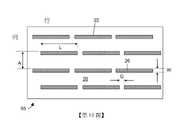
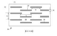
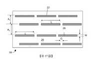
在一具體實施例中,當從上觀看該準直層時,該長型槽被排列成行列,其中長型槽的較長尺度係沿列,及其中該列彼此分開長型槽寬度之至少3倍。當從上觀看該準直層時,該長型槽經常被排列成行列,且同列內的相鄰長型槽分開小於30微米的間隙。在一些具體實施例中,第一列中的相鄰長型槽之間的間隙與第二列中的相鄰長型槽之間的間隙有水平偏位。在一些具體實施例中,改變長型槽長度、長型槽寬度、長型槽節距、或長型槽之間的間隙寬度或配置,而擾亂該長型槽的對稱性。In one embodiment, when the alignment layer is viewed from above, the elongated grooves are arranged in rows, wherein the longer dimensions of the elongated grooves are along the row, and wherein the rows are separated from each other by at least the width of the elongated grooves. 3 times. When the alignment layer is viewed from above, the elongated grooves are often arranged in rows and columns with adjacent elongated grooves in the same row separated by a gap of less than 30 microns. In some embodiments, the gaps between adjacent elongated slots in the first column are horizontally offset from the gaps between adjacent elongated slots in the second column. In some embodiments, the elongated slot length, elongated slot width, elongated slot pitch, or gap width or configuration between elongated slots is altered to disturb the elongated slot symmetry.
本發明之另一態樣包括一種顯示器,其具有光源、可切換的光準直膜、薄膜電晶體主動矩陣、液晶層、及彩色濾光片陣列。該可切換的光準直膜包括第一透光電極層、厚度為至少20微米且包含複數個長型槽之準直層、及第二透光電極層,其中第一及第二透光層分別被配置在該準直層的各一側。該長型槽保有包含顏料粒子之雙穩態電泳流體,且該長型槽經密封層密封,其跨越長型槽開口。Another aspect of the present invention includes a display having a light source, a switchable light-collimating film, a thin film transistor active matrix, a liquid crystal layer, and a color filter array. The switchable light-collimating film includes a first light-transmitting electrode layer, a collimation layer with a thickness of at least 20 microns and including a plurality of long grooves, and a second light-transmitting electrode layer, wherein the first and second light-transmitting layers are arranged on each side of the collimation layer, respectively. The elongated slot holds a bistable electrophoretic fluid containing pigment particles, and the elongated slot is sealed by a sealing layer that spans the elongated slot opening.
在一些具體實施例中,該光準直膜或顯示器另外包括電壓來源及控制器,而在第一與第二透光電極層之間提供電壓脈衝。在一些具體實施例中,該顯示器包括在該光源與該可切換的光準直膜之間的稜鏡膜。在一些具體實施例中,該顯示器包括在該稜鏡膜與該光源之間的擴散層。在一些具體實施例中,該顯示器包括觸控螢幕層。In some embodiments, the light-collimating film or display additionally includes a voltage source and a controller to provide voltage pulses between the first and second light-transmitting electrode layers. In some embodiments, the display includes a thin film between the light source and the switchable light-collimating film. In some embodiments, the display includes a diffusion layer between the iris film and the light source. In some embodiments, the display includes a touch screen layer.
如上所示,本發明提供一種光準直膜,其包括雙穩態電泳流體之長型槽。此膜本身可用於控制入射透射性基板之光之量及/或方向。此膜亦可被整合到裝置中,如LCD顯示器,而提供有用的特徵,如觀看LCD顯示器之使用者的防窺區。因為該光準直膜為可切換的,故使用者可隨選改變發射光之準直。另外,因為介質為雙穩態,故準直狀態會穩定一段時間,例如數分鐘,例如數小時,例如數日,例如數月,而不必對該光準直膜提供額外的能量。As indicated above, the present invention provides a light-collimating film comprising elongated grooves of bistable electrophoretic fluid. The film itself can be used to control the amount and/or direction of light incident on the transmissive substrate. The film can also be integrated into a device, such as an LCD display, to provide useful features, such as a privacy zone for users viewing the LCD display. Because the light collimating film is switchable, the user can change the collimation of the emitted light on demand. In addition, because the medium is bistable, the collimation state is stable for a period of time, such as minutes, such as hours, such as days, such as months, without having to provide additional energy to the light-collimating film.
本發明使用輥對輥製程而能節省成本地製造可切換的光準直膜。因而製造大片可切換的光準直膜為可行的,其可在其他的組裝製程期間被加入裝置中,如LCD顯示器之製作。此膜可包括輔助性光學透明黏著層及離形片,因而可將光準直膜以成品運送及配送。該光準直膜亦可用於零件市場光控制,例如會議室窗戶、建築物外窗、及天窗與天井窗。The present invention enables the cost-effective manufacture of switchable light-collimating films using a roll-to-roll process. It is thus feasible to manufacture large sheets of switchable light-collimating films that can be incorporated into devices during other assembly processes, such as the fabrication of LCD displays. The film may include auxiliary optically clear adhesive layers and release sheets, thereby allowing the light-collimating film to be shipped and distributed as a finished product. The light collimating films can also be used for aftermarket light control, such as conference room windows, building exterior windows, and skylights and patio windows.
電泳顯示器通常包含一層電泳材料、及至少二配置於該電泳材料的對立側之其他層,此二層之一為電極層。在大部分的此種顯示器中,兩層均為電極層,且電極層之一或兩者被圖樣化而界定顯示器像素。例如一電極層可被圖樣化成為長型列電極,及另一被圖樣化成為與列電極呈直角配置的長型行電極,像素係由行列電極交叉處界定。或者且更常為,一電極層為單一連續電極形式,且另一電極層被圖樣化成為像素電極矩陣,其各界定顯示器之一像素。在一些具體實施例中使用二透光電極層,因而可使光穿過電泳顯示器。An electrophoretic display usually includes a layer of electrophoretic material and at least two other layers disposed on opposite sides of the electrophoretic material, and one of the two layers is an electrode layer. In most such displays, both layers are electrode layers, and one or both of the electrode layers are patterned to define display pixels. For example, one electrode layer can be patterned as elongated column electrodes, and the other as elongated row electrodes arranged at right angles to the column electrodes, with pixels defined by the intersections of the row and column electrodes. Alternatively and more commonly, one electrode layer is in the form of a single continuous electrode, and the other electrode layer is patterned into a matrix of pixel electrodes, each of which defines a pixel of the display. Two light transmissive electrode layers are used in some embodiments, thus allowing light to pass through the electrophoretic display.
術語「雙穩態」及「雙穩態性」在此以其在所屬技術領域之習知意義使用,以指稱包含具有至少一種光學性質不同的第一及第二顯示狀態之顯示元件之顯示器,使得在藉有限時間的定址脈衝,驅動任何特定元件達到假設其第一或第二狀態,且在定址脈衝終止後,該狀態會持續歷時改變該顯示元件狀態所需最短定址脈衝時間之至少數倍,例如至少4倍。美國專利第7,170,670號證明,其中一些可有灰階之粒子系電泳顯示器不僅在其極端黑色及白色狀態下穩定,亦在其中間灰色狀態下穩定,且一些其他型式的光電顯示器亦同。此型顯示器應稱為「多穩態」而非雙穩態,雖然在此為了方便可使用術語「雙穩態」涵蓋雙穩態及多穩態顯示器。The terms "bistable" and "bistable" are used herein in their conventional senses in the art to refer to a display that includes display elements having at least one first and second display state that differ in optical properties, such that, by means of a finite-time addressing pulse, any particular element is driven to a hypothetical first or second state, and after termination of the addressing pulse, that state persists for at least several times the minimum addressing pulse time required to change the state of the display element , for example at least 4 times. US Patent No. 7,170,670 demonstrates that some of these particle-based electrophoretic displays, which may have gray scales, are stable not only in their extreme black and white states, but also in their intermediate gray states, as are some other types of electro-optical displays. This type of display should be referred to as "multi-stable" rather than bistable, although the term "bistable" may be used herein for convenience to cover both bistable and multi-stable displays.
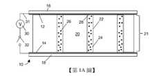
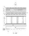
可切換的光準直膜(10)之一般功能示於第1A-1F圖。膜(10)包括第一(12)及第二(14)透光電極層。一般而言,各電極層分別帶有第一基板(16)及第二基板(18)。第一(16)及第二(18)基板可為透光聚合物(例如膜或樹脂)或玻璃。在以輥對輥加工來製造膜(10)的情況,第一(16)及第二(18)基板為撓性。該透光電極及基板亦可被整合到單層中,例如PET-ITO膜、PEDOT,或者為摻有導電性材料(例如石墨烯、奈米管、金屬屑、導電性金屬氧化物粒子、或金屬纖維)及/或摻有導電性單體或聚合物及/或摻有離子性材料(如鹽)之另一種透光聚合物。The general function of the switchable light-collimating film (10) is shown in Figures 1A-1F. The film (10) includes first (12) and second (14) light transmissive electrode layers. Generally, each electrode layer has a first substrate (16) and a second substrate (18), respectively. The first (16) and second (18) substrates may be light transmissive polymers (eg, films or resins) or glass. When the film (10) is produced by roll-to-roll processing, the first (16) and second (18) substrates are flexible. The light-transmitting electrode and substrate can also be integrated into a single layer, such as PET-ITO film, PEDOT, or doped with conductive materials (such as graphene, nanotubes, metal chips, conductive metal oxide particles, or metal fibers) and/or another light transmissive polymer doped with conductive monomers or polymers and/or doped with ionic materials such as salts.
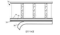
光準直層(21)包含透光聚合物(20),其已經加工而製造複數個長型槽(22)以保有包括電泳粒子(26)之雙穩態電泳流體(24)。在一具體實施例中,雙穩態電泳流體(24)包括烴溶劑,及電泳粒子(26)包含碳黑(視情況被官能化,如以下所討論)。光準直層為至少20微米厚(即第一(12)與第二(14)透光電極層之間的距離)。光準直層可比20微米厚,例如比30微米厚,例如比50微米厚,例如比70微米厚,例如比100微米厚,例如比150微米厚,例如比200微米厚。以下更為詳述長型槽之製作,例如藉由壓印熱塑物。在填充長型槽(22)之製程之後或期間,將長型槽(22)以密封層(28)密封,該密封層(28)可為例如不與雙穩態電泳流體(24)相容之親水性聚合物。The light collimating layer (21) comprises a light transmissive polymer (20) that has been processed to create a plurality of elongated grooves (22) to hold a bistable electrophoretic fluid (24) comprising electrophoretic particles (26). In a specific embodiment, the bistable electrophoretic fluid (24) comprises a hydrocarbon solvent, and the electrophoretic particles (26) comprise carbon black (optionally functionalized, as discussed below). The light-collimating layer is at least 20 microns thick (ie, the distance between the first (12) and second (14) light-transmitting electrode layers). The light collimating layer may be thicker than 20 microns, eg thicker than 30 microns, eg thicker than 50 microns, eg thicker than 70 microns, eg thicker than 100 microns, eg thicker than 150 microns, eg thicker than 200 microns. The production of elongated grooves, for example by stamping thermoplastics, is described in more detail below. After or during the process of filling the elongated groove (22), the elongated groove (22) is sealed with a sealing layer (28), which may be, for example, incompatible with the bistable electrophoretic fluid (24). the hydrophilic polymer.
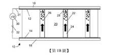
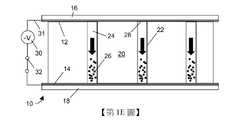
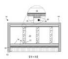
為了改變膜(10)的準直性質,其可將第一(12)及第二(14)透光電極層連結電位來源(30)。該來源可為例如電池、電源供應器、光伏電池、或一些其他的電位來源。該來源可提供簡單DC電位,或者其可被設計成提供時間變動電壓,例如「波形」,如以下所述。第一(12)及第二(14)透光電極層可經電極、電線、或佈線(31)連結來源(30)。在一些具體實施例中,佈線(31)可被開關(32)中斷,其可為例如電晶體開關。第一(12)與第二(14)透光電極層之間的電位一般為至少1伏特,例如至少2伏特,例如至少5伏特,例如至少10伏特,例如至少15伏特,例如至少18伏特,例如至少25伏特,例如至少30伏特,例如至少50伏特。In order to alter the collimation properties of the film (10), it is possible to connect the first (12) and second (14) light-transmitting electrode layers to a potential source (30). The source may be, for example, a battery, a power supply, a photovoltaic cell, or some other source of electrical potential. The source can provide a simple DC potential, or it can be designed to provide a time-varying voltage, such as a "waveform," as described below. The first (12) and second (14) light-transmitting electrode layers can be connected to the source (30) via electrodes, wires, or wirings (31). In some embodiments, the wiring (31) may be interrupted by a switch (32), which may be, for example, a transistor switch. The potential between the first (12) and second (14) light-transmitting electrode layers is generally at least 1 volt, such as at least 2 volts, such as at least 5 volts, such as at least 10 volts, such as at least 15 volts, such as at least 18 volts, For example at least 25 volts, such as at least 30 volts, such as at least 50 volts.
因為雙穩態電泳流體(24)為雙穩態,故不必施加電場而維持電泳粒子(26)之分布。此特徵詳述於在此列出的E Ink Corporation專利,但是主要由雙穩態電泳流體(24)中具有被分布聚合物(例如聚異丁烯或聚甲基丙烯酸月桂酯)的指定混合物所致,使得電泳粒子(26)經由絮凝耗盡而被穩定化。因而在第1A圖所描述的第一狀態中,電泳粒子(26)穩定為分散狀態,儘管在第一(12)與第二(14)透光電極層之間不施加電位。施加適當的電位,例如第1B圖所描述,則電泳粒子(26)朝向經適當偏壓的電極層移動,而沿長型槽(22)的高度製造透光梯度。一旦電泳粒子(26)被驅動到所欲電極層,則來源(30)可脫離該電極層而關閉電位。然而,因為雙穩態電泳流體(24)的雙穩態性,電泳粒子(26)會長時間維持在第二狀態,例如數分鐘、例如數小時,例如數日,如第1C圖所示。Because the bistable electrophoretic fluid (24) is bistable, it is not necessary to apply an electric field to maintain the distribution of the electrophoretic particles (26). This feature is detailed in the E Ink Corporation patents listed here, but is primarily due to having a specified mixture of distributed polymers (eg, polyisobutylene or polylauryl methacrylate) in the bistable electrophoretic fluid (24), The electrophoretic particles (26) are made to be stabilized via flocculation depletion. Thus in the first state depicted in Figure 1A, the electrophoretic particles (26) are stabilized in a dispersed state, although no potential is applied between the first (12) and second (14) light-transmitting electrode layers. Applying an appropriate potential, such as depicted in Figure 1B, causes the electrophoretic particles (26) to move towards the appropriately biased electrode layer, creating a light transmission gradient along the height of the elongated slot (22). Once the electrophoretic particles (26) are driven to the desired electrode layer, the source (30) can break away from the electrode layer to turn off the potential. However, because of the bistable nature of the bistable electrophoretic fluid (24), the electrophoretic particles (26) may remain in the second state for extended periods of time, such as minutes, such as hours, such as days, as shown in Figure 1C.
光準直膜(10)的狀態可藉由以反極性電壓(未示)驅動收集的電泳粒子(26)離開電極完成第1D圖而反轉。在回到最初狀態時(等於第1A圖),僅(約略)準直光可經過光準直膜,如以下更為詳述。第1D圖的狀態亦穩定。電泳粒子(26)可因施加第1B圖之反極性電壓而被驅動通過此分布狀態且朝向第二透光電極(14),如第1E圖所示。結果鄰近第二透光電極(14)而收集電泳粒子(26),其亦造成寬視角,如以下所討論。示於第1F圖之廣角透射狀態亦為雙穩態,即維持此狀態無需電力。因為第1C圖及第1F圖的狀態均造成廣角透射,故可在第1A、1C、1D、與1F圖所示狀態之間轉換,且維持驅動電子學的整體DC均衡。以DC均衡驅動電子學減少電荷累積及延長系統組件的壽命。The state of the light-collimating film (10) can be reversed by driving the collected electrophoretic particles (26) away from the electrodes with a voltage of reverse polarity (not shown) completing the 1D diagram. Upon returning to the initial state (equivalent to Figure 1A), only (roughly) collimated light can pass through the light-collimating film, as described in more detail below. The state of Fig. 1D is also stable. The electrophoretic particles (26) can be driven through this distribution and towards the second light-transmitting electrode (14) by applying the reverse polarity voltage of Figure 1B, as shown in Figure 1E. As a result, electrophoretic particles (26) are collected adjacent to the second light-transmitting electrode (14), which also results in a wide viewing angle, as discussed below. The wide-angle transmission state shown in Figure IF is also bistable, ie no power is required to maintain this state. Because the states of Figures 1C and 1F both result in wide-angle transmission, it is possible to switch between the states shown in Figures 1A, 1C, 1D, and 1F while maintaining overall DC balance of the drive electronics. Drive electronics with DC balance to reduce charge accumulation and extend the life of system components.
電泳介質的內相包括帶電顏料粒子於懸浮流體。用於本發明之可變透射介質的流體一般為低介電常數(較佳為小於10且希望為小於3)。特佳溶劑包括脂肪族烴,如庚烷、辛烷,及石油餾液,如Isopar® (Exxon Mobil)或Isane® (Total);萜烯,如檸檬烯,例如1-檸檬烯;及芳香族烴,如甲苯。特佳溶劑為檸檬烯,因為其兼具低介電常數(2.3)及相當高的折射率(1.47)。內相的折射率可藉由添加折射率匹配劑而修改,如得自Cargille-Sacher Laboratories Inc. (Cedar Grove, NJ)之Cargille®折射率匹配流體。在本發明之封裝的介質中,較佳為粒子分散液的折射率僅可能接近地匹配封裝材料以降低霧化。當溶劑的折射率接近封裝劑時,最佳地得到此折射率匹配(使用常用的聚合封裝劑時)。在大部分的情況,內相的550奈米折射率在1.51至1.57之間為有益的,在550奈米較佳為約1.54。The internal phase of the electrophoretic medium includes charged pigment particles in a suspending fluid. Fluids used in the variable transmission medium of the present invention are generally low dielectric constants (preferably less than 10 and desirably less than 3). Particularly preferred solvents include aliphatic hydrocarbons, such as heptane, octane, and petroleum distillates, such as Isopar® (Exxon Mobil) or Isane® (Total); terpenes, such as limonenes, such as 1-limonene; and aromatic hydrocarbons, such as toluene. A particularly preferred solvent is limonene because of its low dielectric constant (2.3) and relatively high refractive index (1.47). The index of refraction of the internal phase can be modified by adding index matching agents, such as Cargille® index matching fluids from Cargille-Sacher Laboratories Inc. (Cedar Grove, NJ). In the encapsulated medium of the present invention, it is preferred that the refractive index of the particle dispersion is only as close as possible to match the encapsulation material to reduce fogging. This index matching is best obtained when the index of refraction of the solvent is close to that of the encapsulant (when using common polymeric encapsulants). In most cases, an index of refraction at 550 nm of the internal phase is advantageously between 1.51 and 1.57, preferably about 1.54 at 550 nm.
帶電顏料粒子可為各種顏色及組成物。另外,帶電顏料粒子可經表面聚合物官能化以改良狀態穩定性。此顏料揭述於美國專利公開第2016/0085132號,其全部納入作為參考。例如若帶電粒子為白色,則其可由無機顏料形成,如TiO2、ZrO2、ZnO、Al2O3、Sb2O3、BaSO4、PbSO4等。其亦可為折射率高(>1.5)及具有特定大小(>100奈米)以呈現白色之聚合物粒子,或經改造而具有所欲折射率之複合粒子。黑色帶電粒子可由CI顏料黑26或28等(例如鐵錳黑尖晶石或鉻銅黑尖晶石)或碳黑形成。其他的顏色(非白及非黑)可由有機顏料形成,如CI顏料PR 254、PR122、PR149、PG36、PG58、PG7、PB28、PB15:3、PY83、PY138、PY150、PY155、或PY20。其他的實例包括Clariant Hostaperm紅D3G 70-EDS、Hostaperm粉紅E-EDS、PV堅牢紅D3G、Hostaperm紅D3G 70、Hostaperm藍B2G-EDS、Hostaperm黃H4G-EDS、Novoperm黃HR-70-EDS、Hostaperm綠GNX、BASF Irgazine紅L 3630、Cinquasia紅L 4100 HD、與Irgazin紅L 3660 HD;Sun Chemical酞青藍、酞青綠、二芳基黃、或二芳基AAOT黃。亦可由無機顏料形成彩色粒子,如CI顏料藍28、CI顏料綠50、CI顏料黃227等。帶電粒子的表面可經基於所需的粒子電荷極性及電荷程度之已知技術修改,如美國專利第6,822,782、7,002,728、9,366,935、與9,372,380號,以及美國專利公開第2014-0011913號所揭述,其內容均全部納入此處作為參考。The charged pigment particles can be of various colors and compositions. Additionally, charged pigment particles can be functionalized with surface polymers to improve state stability. This pigment is disclosed in US Patent Publication No. 2016/0085132, which is incorporated by reference in its entirety. For example, if the charged particles are white, they may be formed from inorganic pigments such asTiO2 ,ZrO2 , ZnO,Al2O3 ,Sb2O3 ,BaSO4 ,PbSO4 , and thelike. It can also be a polymer particle with a high refractive index (>1.5) and a specific size (>100 nm) to appear white, or a composite particle engineered to have a desired refractive index. The black charged particles may be formed from
該粒子可呈現負電荷,或者其可明確使用電荷控制劑充電,或者當被懸浮在溶劑或溶劑混合物中時可獲得電荷。合適的電荷控制劑在所屬技術領域為已知的;其本質可為聚合性或非聚合性,或者可為離子性或非離子性。電荷控制劑之實例可包括但不限於Solsperse 17000(活性聚合分散劑)、Solsperse 9000(活性聚合分散劑)、OLOA 11000(琥珀醯亞胺無灰分散劑)、Unithox 750(乙氧化物)、Span 85(山梨醇三油酸酯)、Petronate L(磺酸鈉)、Alcolec LV30(大豆卵磷脂)、Petrostep B100(石油磺酸鹽)、或B70(磺酸鋇)、Aerosol OT、聚異丁烯衍生物、或聚(乙烯-共聚-丁烯)衍生物等。除了懸浮流體及帶電的顏料粒子,內相亦可包括穩定劑、界面活性劑、及電荷控制劑。穩定化材料當被分散於溶劑中時可被吸附在帶電顏料粒子上。此穩定化材料將粒子保持彼此分離,使得當粒子處於其分散狀態時,該可變透射介質為實質上非透射性。所屬技術領域已知,將帶電粒子(如上所述,一般為碳黑)分散於低介電常數溶劑中可使用界面活性劑輔助。此界面活性劑一般包含極性「頭基」、及相容或溶於溶劑之非極性「尾基」。本發明較佳為非極性尾基為飽和或不飽和烴部分,或其他溶於烴溶劑之基,例如聚(二烷基矽氧烷)。該極性基可為任何極性有機官能基,包括離子性材料,如銨、磺酸鹽、或膦酸鹽,或酸性或鹼性基。特佳頭基為羧酸或羧酸鹽基。適合用於本發明之穩定劑包括聚異丁烯與聚苯乙烯。在一些具體實施例中添加分散劑,如聚異丁烯琥珀醯亞胺及/或山梨醇三油酸酯、及/或2-己基癸酸。The particle may exhibit a negative charge, or it may be charged explicitly using a charge control agent, or may acquire a charge when suspended in a solvent or solvent mixture. Suitable charge control agents are known in the art; they may be polymeric or non-polymeric in nature, or ionic or non-ionic in nature. Examples of charge control agents may include, but are not limited to, Solsperse 17000 (living polymeric dispersant), Solsperse 9000 (living polymeric dispersant), OLOA 11000 (succinimidyl ashless dispersant), Unithox 750 (ethoxylated), Span 85 (sorbitan trioleate), Petronate L (sodium sulfonate), Alcolec LV30 (soy lecithin), Petrostep B100 (petroleum sulfonate), or B70 (barium sulfonate), Aerosol OT, polyisobutylene derivatives , or poly(ethylene-co-butene) derivatives, etc. In addition to the suspending fluid and charged pigment particles, the internal phase may also include stabilizers, surfactants, and charge control agents. The stabilizing material can be adsorbed on the charged pigment particles when dispersed in a solvent. This stabilizing material keeps the particles separated from each other such that when the particles are in their dispersed state, the variable transmission medium is substantially non-transmissive. It is known in the art to disperse charged particles (typically carbon black, as described above) in a low dielectric constant solvent with the aid of surfactants. Such surfactants generally contain polar "head groups" and non-polar "tail groups" that are compatible or soluble in solvents. It is preferred in the present invention that the non-polar tail group be a saturated or unsaturated hydrocarbon moiety, or other group soluble in a hydrocarbon solvent, such as poly(dialkylsiloxane). The polar group can be any polar organic functional group, including ionic materials such as ammonium, sulfonate, or phosphonate, or acidic or basic groups. Particularly preferred head groups are carboxylic acid or carboxylate groups. Stabilizers suitable for use in the present invention include polyisobutylene and polystyrene. In some embodiments, dispersants are added, such as polyisobutylene succinimide and/or sorbitan trioleate, and/or 2-hexyldecanoic acid.
本發明之電泳介質一般含有電荷控制劑(CCA),且可含有電荷引導劑。這些電泳介質成分一般包含低分子量界面活性劑、聚合性試劑、或一種或以上的成分的摻合物,且用以穩定或修改電泳粒子上的電荷符號及/或量級。CCA一般為包含離子性或其他極性基之分子,其在以下稱為頭基。較佳為至少一個正或負離子性頭基附接非極性鏈(一般為烴鏈),其在以下稱為尾基。據信CCA在內相中形成逆微胞,及僅少數帶電逆微胞即在一般作為電泳流體之非常非極性流體中產生導電度。The electrophoretic media of the present invention generally contain a charge control agent (CCA), and may contain a charge director. These electrophoretic medium components typically comprise low molecular weight surfactants, polymeric agents, or blends of one or more components, and are used to stabilize or modify the sign and/or magnitude of charge on the electrophoretic particles. CCAs are generally molecules containing ionic or other polar groups, hereinafter referred to as head groups. Preferably at least one positively or negatively ionic head group is attached to a non-polar chain (generally a hydrocarbon chain), hereinafter referred to as a tail group. It is believed that CCA forms inverse micelles in the internal phase, and that only a few charged inverse micelles create conductivity in very non-polar fluids that are typically electrophoretic fluids.
逆微胞包含被CCA分子之非極性尾基包圍的高極性核(一般含有水),其大小可為1奈米至數十奈米(且可為球形、圓柱形、或其他的幾何)。逆微胞已被廣泛研究,尤其是如油/水/界面活性劑混合物的三元混合物。一實例為異辛烷/水/AOT混合物,例如在Fayer等人之J. Chem. Phys.,131, 14704 (2009)中所揭述。電泳介質中一般可分為三相:具有表面之固體粒子、以極小滴之形式分布的高極性相(逆微胞)、及包含流體之連續相。在施加電場時,帶電粒子及帶電逆微胞均可移動通過流體,因此通過流體(其一般本身的導電度極小)導電有2種平行路徑。Inverse micelles contain a highly polar core (generally containing water) surrounded by non-polar tails of CCA molecules, which can be 1 to tens of nanometers in size (and can be spherical, cylindrical, or other geometries). Inverse micelles have been extensively studied, especially ternary mixtures such as oil/water/surfactant mixtures. An example is isooctane/water/AOT mixtures such as described in Fayer et al., J. Chem. Phys.,131 , 14704 (2009). There are generally three phases in an electrophoretic medium: solid particles with a surface, a highly polar phase (inverse micelles) distributed in the form of tiny droplets, and a continuous phase containing a fluid. When an electric field is applied, both charged particles and charged inverse cells can move through the fluid, so there are 2 parallel paths of conduction through the fluid (which generally has little conductivity itself).
據信CCA之極性核因吸附在表面上而影響表面上的電荷。在電泳顯示器中,此吸附可在電泳粒子表面或微囊內壁(或其他的固相,如微胞壁)上,而形成類似逆微胞之結構,這些結構在以下稱為半微胞。當離子對之一離子比另一離子較強烈地附接表面時(例如因共價鍵結),半微胞與未鍵結逆微胞之間的離子交換可導致電荷分離,其中較強烈鍵結離子仍結合粒子,較不強烈鍵結的離子則被併入自由逆微胞之核中。It is believed that the polar nuclei of CCA affect the charge on the surface by being adsorbed on the surface. In an electrophoretic display, the adsorption can be on the surface of electrophoretic particles or the inner wall of the microcapsule (or other solid phase, such as the wall of the micelle) to form structures similar to inverse micelles, which are hereinafter referred to as half-cells. When one ion of an ion pair is more strongly attached to a surface than the other (eg, due to covalent bonding), ion exchange between half-cells and unbonded inverse cells can lead to charge separation, where the stronger bonds The bound ions remain bound to the particles, and the less strongly bound ions are incorporated into the nuclei of free inverse cells.
亦可能為形成CCA之頭基的離子性材料會在電泳粒子(等)表面處誘發離子對形成。因此,CCA可實行2種基本功能:在表面處產生電荷及電荷從表面分離。電荷產生可由存在於CCA分子中或被加入逆微胞核或流體中的某些部分、與粒子表面之間的酸-鹼或離子交換反應造成。因此,可使用的CCA材料為可參與此反應者,或所屬技術領域已知的任何其他充電反應。CCA分子可另外作為由電泳粒子(當以光照射該粒子時)產生的光-激子之受體。It is also possible that the ionic material forming the head group of the CCA induces ion pair formation at the surface of the electrophoretic particle (etc.). Thus, CCA can perform two basic functions: charge generation at the surface and charge separation from the surface. Charge generation can result from acid-base or ion exchange reactions between certain moieties present in the CCA molecule or added to the inverse micronucleus or fluid, and the particle surface. Thus, CCA materials that can be used are those that can participate in this reaction, or any other charging reaction known in the art. CCA molecules can additionally act as acceptors for photo-excitons generated by electrophoretic particles when the particles are irradiated with light.
可用於本發明介質之非限制種類的電荷控制劑包括有機硫酸鹽或磺酸鹽、金屬皂、嵌段或梳形共聚物、有機醯胺、有機兩性離子、及有機磷酸鹽與膦酸鹽。可使用的有機硫酸鹽及磺酸鹽包括但不限於雙(2-乙基己基)鱑琥珀酸鈉、十二碳基苯磺酸鈣、石油磺酸鈣、中性或鹼性二壬基萘磺酸鋇、中性或鹼性二壬基萘磺酸鈣、十二碳基苯磺酸鈉鹽、及月桂基硫酸銨。可使用的金屬皂包括但不限於鹼性或中性石油磺酸鋇(barium petronate)、石油磺酸鈣、羧酸(如環烷酸、辛酸、油酸、棕櫚酸、硬脂酸、與肉豆蔻酸等)之鈷、鈣、銅、錳、鎂、鎳、鋅、鋁、與鐵鹽。可使用的嵌段或梳形共聚物包括但不限於(A)經對甲苯磺酸甲酯四級化之甲基丙烯酸2-(N,N-二甲胺基)乙酯之聚合物、與(B)聚(甲基丙烯酸2-乙基己酯)之AB二嵌段共聚物,及具有聚(12-羥基硬脂酸)之油溶性尾,並側接聚(甲基丙烯酸甲酯-甲基丙烯酸)之油溶性錨定基,且分子量為約1800的梳形接枝共聚物。可使用的有機醯胺/胺包括但不限於聚異丁烯琥珀醯亞胺,如OLOA 371或1200(得自德州休士頓之Chevron Oronite Company LLC)、或Solsperse 17000(得自俄亥俄州Wickliffe之Lubrizol,Solsperse為註冊商標),及N-乙烯基吡咯啶酮聚合物。可使用的有機兩性離子包括但不限於卵磷脂。可使用的有機磷酸鹽與膦酸鹽包括但不限於具有飽和及不飽和酸取代基之磷酸化單及二甘油酯之鈉鹽。可用於CCA之尾基包括烯烴聚合物,如分子量為200-10,000之範圍的聚(異丁烯)。頭基可為磺酸、磷酸、或羧酸或醯胺,或者可為胺基,如一級、二級、三級、或四級銨基。Non-limiting classes of charge control agents useful in the media of the present invention include organic sulfates or sulfonates, metal soaps, block or comb copolymers, organic amides, organic zwitterions, and organic phosphates and phosphonates. Useful organic sulfates and sulfonates include, but are not limited to, sodium bis(2-ethylhexyl) succinate, calcium dodecylbenzenesulfonate, calcium petroleum sulfonate, neutral or basic dinonylnaphthalene Barium sulfonate, neutral or basic calcium dinonylnaphthalenesulfonate, sodium dodecylbenzenesulfonate, and ammonium lauryl sulfate. Metal soaps that can be used include, but are not limited to, basic or neutral barium petronate, calcium petronate, carboxylic acids such as naphthenic acid, caprylic acid, oleic acid, palmitic acid, stearic acid, and meat. myristic acid, etc.) cobalt, calcium, copper, manganese, magnesium, nickel, zinc, aluminum, and iron salts. Useful block or comb copolymers include, but are not limited to (A) polymers of 2-(N,N-dimethylamino)ethyl methacrylate quaternized with methyl p-toluenesulfonate, and (B) AB diblock copolymer of poly(2-ethylhexyl methacrylate) with an oil-soluble tail of poly(12-hydroxystearic acid) and pendant poly(methyl methacrylate- methacrylic acid), a comb-shaped graft copolymer with an oil-soluble anchor group and a molecular weight of about 1800. Useful organamides/amines include, but are not limited to, polyisobutylene succinimides such as OLOA 371 or 1200 (available from Chevron Oronite Company LLC, Houston, Texas), or Solsperse 17000 (available from Wickliffe, Ohio, Lubrizol, Solsperse is a registered trademark), and N-vinylpyrrolidone polymers. Organic zwitterions that can be used include, but are not limited to, lecithin. Useful organophosphates and phosphonates include, but are not limited to, the sodium salts of phosphorylated mono- and diglycerides with saturated and unsaturated acid substituents. Useful tails for CCA include olefin polymers such as poly(isobutylene) having a molecular weight in the range of 200-10,000. The head group can be a sulfonic acid, phosphoric acid, or carboxylic acid or amide, or it can be an amine group such as a primary, secondary, tertiary, or quaternary ammonium group.
用於本發明介質之電荷佐劑可將電泳粒子表面上的電荷偏壓,如以下更為詳述。此電荷佐劑可為布忍斯特或路易士酸或鹼。The charge adjuvants used in the media of the present invention can bias the charge on the surface of electrophoretic particles, as described in more detail below. This charge adjuvant can be a Brünster or Lewis acid or base.
其可添加粒子分散穩定劑以防止粒子絮凝或附接囊或壁或表面。對於在電泳顯示器中作為流體之典型高電阻液體,其可使用非水性界面活性劑。其包括但不限於二醇醚、乙炔二醇、烷醇醯胺、山梨醇衍生物、烷胺、四級胺、咪唑啉、二烷基氧化物、及磺琥珀酸酯。It can add particle dispersion stabilizers to prevent particles from flocculating or attaching to capsules or walls or surfaces. For typical high resistance liquids as fluids in electrophoretic displays, non-aqueous surfactants can be used. These include, but are not limited to, glycol ethers, acetylene glycols, alkanolamides, sorbitol derivatives, alkylamines, quaternary amines, imidazolines, dialkyl oxides, and sulfosuccinates.
如美國專利第7,170,670號所揭述,電泳介質的雙穩態性可藉由在流體中包括數量平均分子量超過約20,000之聚合物而改良,此聚合物本質上對電泳粒子為非吸附性;聚(異丁烯)為用於此目的之較佳聚合物。As disclosed in US Pat. No. 7,170,670, the bistability of electrophoretic media can be improved by including in the fluid a polymer having a number average molecular weight in excess of about 20,000 that is essentially non-adsorbent to electrophoretic particles; (isobutylene) is the preferred polymer for this purpose.
另外,如例如美國專利第6,693,620號所揭述,表面上具有固定電荷之粒子在包圍流體中建立電荷相反的電雙層。CCA之離子性頭基可與電泳粒子表面上的帶電基成離子配對,而形成一層固定或部分固定帶電物種。在此層外部有包含帶電(逆)微胞(在流體中包含CCA分子)之擴散層。在習知DC電泳中,施加的電場對固定的表面電荷施力且對移動的對立電荷施以相反力,使得在該擴散層內部發生滑動及粒子相對流體而移動。已知滑動面處的電位為仄他電位。Additionally, particles with a fixed charge on the surface create an oppositely charged electric double layer in the surrounding fluid, as disclosed, for example, in US Pat. No. 6,693,620. The ionic head groups of CCA can ionically pair with charged groups on the surface of electrophoretic particles to form a layer of immobilized or partially immobilized charged species. Outside this layer there is a diffusion layer containing charged (reverse) micelles containing CCA molecules in the fluid. In conventional DC electrophoresis, an applied electric field exerts a force on fixed surface charges and an opposite force on moving opposing charges, so that sliding occurs inside the diffusion layer and particles move relative to the fluid. The potential at the sliding surface is known as the zeta potential.
生成的光準直膜(10)可用以將光(33)窄化(準直),如第2A、2B、及2C圖所示。在第一窄化狀態,如第2A圖所示,電泳粒子(26)被分布遍及長型槽(22)而生成透射角θ1,其由長型槽(22)之間的節距(A)、各長型槽(22)的寬度(W)、光準直膜(10)的高度(H)、及從光源(33)到離開基板(在第2A圖之實例中為基板(18))的距離所界定。由第2A圖可知,θ1角約略由光線X-X’及Y-Y’界定,其界定光可離開光源(33)且使被電泳粒子(26)分布遍及的長型槽(22)上下方所擷取的間距之從正交起最大角度。The resulting light collimating film (10) can be used to narrow (collimate) light (33), as shown in Figures 2A, 2B, and 2C. In the first narrowed state, as shown in Figure 2A, the electrophoretic particles (26) are distributed throughout the elongated grooves (22) to generate a transmission angleθ1 , which is determined by the pitch (A) between the elongated grooves (22). ), the width (W) of each elongated slot (22), the height (H) of the light-collimating film (10), and the distance from the light source (33) to the substrate (in the example of Fig. 2A, the substrate (18) ) is defined by the distance. As can be seen from Fig. 2A, the angleθ1 is roughly defined by rays XX' and YY', which define the upper and lower grooves (22) where the light can leave the light source (33) and distribute the electrophoretic particles (26) throughout. The maximum angle from the orthogonality of the distances captured by the square.
在第一廣角狀態中,其相當於以上第1C圖,電泳粒子(26)被驅動到較近的基板(16),且由光線X-X’及Y-Y’建立新透射角θ2,如第2B圖所示。新透射角θ2遠比θ1寬,如第2B圖所示,即θ2>>θ1。透射角θ2之有效窄化再度為長型槽(22)之間的節距(A)、各長型槽(22)的寬度(W)、及光準直膜(10)的高度(H)之函數。In the first wide angle state, which corresponds to Figure 1C above, the electrophoretic particles (26) are driven to the closer substrate (16) and a new transmission angleθ2 is established from the rays XX' and YY', As shown in Figure 2B. The new transmission angleθ2 is much wider thanθ1 , as shown in Figure 2B, ieθ2 >>θ1 . The effective narrowing of the transmission angleθ2 is again the pitch (A) between the elongated grooves (22), the width (W) of each elongated groove (22), and the height (H) of the light-collimating film (10) ) function.
在第二廣角狀態中,其相當於以上第1F圖,電泳粒子(26)被驅動到離開光源(33)的基板(16),且由光線X-X’及Y-Y’建立新透射角θ3,如第2C圖所示。新透射角θ3遠比θ1寬,如第2C圖所示,即θ3>>θ1。如同第2B圖,透射角θ3之有效窄化為長型槽(22)之間的節距(A)、各長型槽(22)的寬度(W)、及光準直膜(10)的高度(H)之函數。此外,雖然似乎鄰接第二基板(18)而累積的電泳粒子(26)會造成陰影,但未觀察到。其推測為有充分的散射光通過光準直膜(10)而掃除此效應。In the second wide angle state, which corresponds to Figure 1F above, the electrophoretic particles (26) are driven to the substrate (16) away from the light source (33) and a new transmission angle is established from the rays XX' and YY'θ3 , as shown in Figure 2C. The new transmission angleθ3 is much wider thanθ1 , as shown in Figure 2C, ieθ3 >>θ1 . As in Figure 2B, the effective narrowing of the transmissionangle θ3 is the pitch (A) between the elongated grooves (22), the width (W) of each elongated groove (22), and the light-collimating film (10) function of the height (H). Furthermore, although the electrophoretic particles ( 26 ) that accumulate adjacent to the second substrate ( 18 ) appear to cause shadows, they are not observed. It is presumed that there is sufficient scattered light passing through the light collimating film (10) to sweep away this effect.
預期在大部分的組態中,本發明之光準直膜(10)從寬透射角(第2B及2C圖)轉移到窄透射角(第2A圖)提供至少縮小2倍的有效觀看面積(界定為如從正交起之角的函數之相對透射小於50%)。在一些具體實施例中,該觀看面積減小大於2倍,例如3倍,例如4倍。因為此功能,光準直膜(10)當簡單施加於玻璃板時為有用的,例如辦公室內窗,藉此可大為減小玻璃的透射角,因而對辦公室使用者提升防窺且同時可使良好的光量穿越窗戶。It is expected that in most configurations, the light-collimating film (10) of the present invention transitions from a wide transmission angle (Figs. 2B and 2C) to a narrow transmission angle (Fig. 2A) to provide at least a 2X reduction in effective viewing area ( Defined as less than 50% relative transmission as a function of angle from normal). In some embodiments, the viewing area reduction is greater than a factor of 2, such as a factor of 3, such as a factor of 4. Because of this function, the light-collimating film (10) is useful when simply applied to a glass sheet, such as an office interior window, whereby the transmission angle of the glass can be greatly reduced, thereby improving privacy for office users and at the same time Get a good amount of light through the window.
光準直膜(10)可被併入液晶顯示器(LCD)堆集(stack)中,如第3圖所示。第3圖為例示性,因為LCD堆集有許多不同的組態。如第3圖所示,一般為一個或以上的發光二極體(LED)之光(33)被導光板(34)與擴散板(35)的組合引導通過顯示器堆集,包括主動式層。以觀看者方向(眼睛在第3圖上方)行進的離開擴散板(35)之光接著遭遇上述型式的光準直膜(10)。在第3圖所示狀態中,光準直膜(10)僅讓在較窄透射角(參見第2圖)內行進之光通過該主動式層。未穿過光準直膜(10)之光接著前進通過第一偏光膜(36),其為包括複數個像素電極(42)之主動矩陣薄膜電晶體(AM-TFT)陣列(40)。通過AM-TFT (40)及像素電極(42)之偏光然後遭遇液晶層(44),藉此可藉液晶操縱光偏光,使得光穿越第二偏光膜(37)或被退回。特定而言,液晶層(44)的光學狀態因在像素電極與前電極(45)之間提供電場而改變,如LCD顯示器技術領域所已知。穿越光準直膜(10)、AM-TFT (40)、像素電極(42)、液晶層(44)、與前電極(45)之光然後穿越彩色濾光片陣列(46),其僅讓底下像素電極(42)相關的色譜穿過。最後,一些顏色正確且偏光正確(由液晶層決定)之光越過第二偏光膜(37)且被觀看者看到。若需要則各種額外的光學黏著層(47)可被包括在該堆集中。該堆集亦可包括保護罩層(49),其可為例如玻璃或塑膠。額外的元件亦可被加入該堆集,如電容式觸感層(48)或數位層(未示),以得到觸控螢幕能力或書寫力等。第4圖描述包括保護罩層(49)及電容式觸感層(48)。The light collimating film (10) can be incorporated into a liquid crystal display (LCD) stack, as shown in FIG. 3 . Figure 3 is illustrative as there are many different configurations of LCD stacks. As shown in Figure 3, light (33), typically one or more light emitting diodes (LEDs), is directed through the display stack, including active layers, by a combination of light guide plate (34) and diffuser plate (35). Light exiting the diffuser plate (35) traveling in the direction of the viewer (eyes above Figure 3) then encounters a light collimating film (10) of the type described above. In the state shown in Figure 3, the light-collimating film (10) allows only light traveling within a narrow transmission angle (see Figure 2) to pass through the active layer. Light not passing through the light collimating film (10) then proceeds through a first polarizing film (36), which is an active matrix thin film transistor (AM-TFT) array (40) including a plurality of pixel electrodes (42). The polarized light passing through the AM-TFT (40) and the pixel electrode (42) then encounters the liquid crystal layer (44), whereby the light polarization can be manipulated by the liquid crystal so that the light passes through the second polarizing film (37) or is returned. In particular, the optical state of the liquid crystal layer (44) is changed by providing an electric field between the pixel electrode and the front electrode (45), as is known in the art of LCD displays. Light passing through the light collimating film (10), AM-TFT (40), pixel electrode (42), liquid crystal layer (44), and front electrode (45) then passes through the color filter array (46), which only allows The color spectrum associated with the underlying pixel electrode (42) passes through. Finally, some light of the correct color and correct polarization (determined by the liquid crystal layer) passes through the second polarizing film (37) and is seen by the viewer. Various additional optical adhesive layers (47) may be included in the stack if desired. The stack may also include a protective cover layer (49), which may be, for example, glass or plastic. Additional components can also be added to the stack, such as a capacitive touch layer (48) or a digital layer (not shown), for touch screen capability or writing force, etc. Figure 4 depicts the inclusion of a protective cover layer (49) and a capacitive touch layer (48).
第3圖描述的包括光準直膜(10)之LCD堆集的淨效應為可獨立控制從LCD顯示器(例如電腦監視器、智慧型手機、資料終端機、或其他的LCD顯示器)發出之光的透射角。此外,因為切換介質為雙穩態,故該裝置可實際上無限維持「寬」或「窄」狀態。在先進具體實施例中,窄化量可藉由控制被驅動朝向長型槽觀看側之顏料的相對量而調整。透射角可完全無關LCD狀態而調整。即不必關閉監視器以切換防窺及非防窺模式。The net effect of the LCD stack including the light-collimating film (10) depicted in Figure 3 is that the light emitted from an LCD display (such as a computer monitor, smartphone, data terminal, or other LCD display) can be independently controlled. transmission angle. Furthermore, because the switching medium is bistable, the device can maintain a "wide" or "narrow" state virtually indefinitely. In advanced embodiments, the amount of narrowing can be adjusted by controlling the relative amount of pigment that is driven toward the viewing side of the elongated slot. The transmission angle can be adjusted completely independent of the LCD state. That is, it is not necessary to turn off the monitor to switch between privacy and non-privacy modes.
在其他具體實施例中,為了增加被以正確定向引導朝向光準直膜(10)而穿過光準直膜(10)之入射光量,其可將額外的稜鏡膜(50)加入光學元件堆集,如第5圖所示。合併稜鏡膜(50)會造成顯示器強度稍具角相依性,然而,顯示器堆集的總效率改良且造成電力消耗較小。此特徵對例如行動裝置(如膝上型電腦或電話)可能為急需的。In other embodiments, in order to increase the amount of incident light that is directed towards the light-collimating film (10) in the correct orientation through the light-collimating film (10), it is possible to add an additional halide film (50) to the optical element stack, as shown in Figure 5. Incorporating the halide film (50) results in a slight angular dependence of the display intensity, however, the overall efficiency of the display stack improves and results in less power consumption. This feature may be desperately needed for, for example, mobile devices such as laptops or phones.
密封層(28)之一展開圖示於第6圖。在一些具體實施例中,為了持有雙穩態電泳流體(24),密封層(28)將長型槽(22)頂部密封,如該展開圖所示。其可藉由將長型槽(22)底下填充雙穩態電泳流體(24),然後將幾乎全長型槽(22)外敷密封調配物(以下討論)而完成。在其他具體實施例中,該密封組成物可在填充時被分散於雙穩態電泳流體(24)中,且被設計成確可造成密封組成物上升致長型槽(22)頂部之親水力及密度,藉此例如使用光、熱、或暴露於活化化學試劑而硬化。在替代具體實施例中(第6圖未示),長型槽(22)可被填充到頂部,且將密封層散佈在透光聚合物(20)的全部頂部,因而將雙穩態電泳流體(24)密封在長型槽內。An expanded view of one of the sealing layers (28) is shown in FIG. 6 . In some embodiments, to hold the bistable electrophoretic fluid (24), the sealing layer (28) seals the top of the elongated slot (22), as shown in this expanded view. This can be accomplished by filling the bottom of the elongated groove (22) with a bistable electrophoretic fluid (24) and then overcoating the nearly full length of the groove (22) with a sealing formulation (discussed below). In other embodiments, the sealing composition may be dispersed in the bistable electrophoretic fluid (24) during filling, and is designed to cause the sealing composition to rise to cause hydrophilicity at the top of the elongated groove (22). and density, whereby it hardens, for example, using light, heat, or exposure to activating chemicals. In an alternative embodiment (not shown in Figure 6), the elongated grooves (22) may be filled to the top and the sealing layer spread over the entire top of the light transmissive polymer (20), thus bridging the bistable electrophoretic fluid (24) Sealed in the elongated groove.
密封層用之密封組成物中的重要成分之實例可包括但不限於熱塑物或熱固物及其前體。指定實例可包括如單官能基丙烯酸酯、單官能基甲基丙烯酸酯、多官能基丙烯酸酯、多官能基甲基丙烯酸酯、聚乙烯醇、聚丙烯酸、纖維素、明膠等材料。添加劑可被加入該密封組成物,如聚合性黏合劑或增稠劑、光引發劑、觸媒、硫化劑、填料、著色劑或界面活性劑,以改良物理機械性質及光準直膜。Examples of important components in the sealing composition for the sealing layer may include, but are not limited to, thermoplastics or thermosets and their precursors. Specified examples may include materials such as monofunctional acrylates, monofunctional methacrylates, multifunctional acrylates, multifunctional methacrylates, polyvinyl alcohol, polyacrylic acid, cellulose, gelatin, and the like. Additives can be added to the sealing composition, such as polymeric binders or thickeners, photoinitiators, catalysts, vulcanizing agents, fillers, colorants, or surfactants, to improve the physico-mechanical properties and light-collimating films.
該密封組成物可為水溶性聚合物且以水作為密封溶劑。合適的水溶性聚合物或水溶性聚合物前體之實例可包括但不限於聚乙烯醇;聚乙二醇、其與聚丙二醇的共聚物、及其衍生物,如PEG-PPG-PEG、PPG-PEG、PPG-PEG-PPG;聚(乙烯基吡咯啶酮)及其共聚物,如聚(乙烯基吡咯啶酮)/乙酸乙烯酯(PVP/VA);多醣體,如纖維素及其衍生物、聚(葡萄糖胺)、葡聚糖、瓜爾膠、與澱粉;明膠;三聚氰胺-甲醛;聚(丙烯酸)、其鹽形式、及其共聚物;聚(甲基丙烯酸)、其鹽形式、及其共聚物;聚(順丁烯二酸)、其鹽形式、及其共聚物;聚(甲基丙烯酸2-二甲胺基乙酯);聚(2-乙基-2-
可存在於例如黏著劑組成物中的額外成分之實例可包括但不限於丙烯酸類、苯乙烯-丁二烯共聚物、苯乙烯-丁二烯-苯乙烯嵌段共聚物、苯乙烯-異戊二烯-苯乙烯嵌段共聚物、聚乙烯基丁醛、纖維素乙酸酯丁酸酯、聚乙烯基吡咯啶酮、聚胺基甲酸酯類、聚醯胺類、乙烯-乙酸乙烯酯共聚物、環氧化物類、多官能基丙烯酸酯類、乙烯類、乙烯醚類、及其寡聚物、聚合物、及共聚物。黏著層亦可含有聚胺基甲酸酯分散液,及選自由以下組成的群組之水溶性聚合物:聚乙烯醇;聚乙二醇及其與聚丙二醇的共聚物;聚(乙烯基吡咯啶酮)及其共聚物;多醣體;明膠;聚(丙烯酸)、其鹽形式、及其共聚物;聚(甲基丙烯酸)、其鹽形式、及其共聚物;聚(甲基丙烯酸2-二甲胺基乙酯);聚(2-乙基-2-
該堆集全體,例如包括基板(53),可被邊緣密封劑(51)密封,如第6圖所示。邊緣密封劑(51)可包括任何上述的密封組成物。邊緣密封劑(51)可為圍繞光準直層(10)及基板(53)之連續性,或者邊緣密封劑(51)可僅覆蓋該堆集的一部分,例如僅光準直層(10)外緣。在一些具體實施例中,邊緣密封劑(51)可包括額外的保護層,例如不透水之層,例如透明聚乙烯。該保護層可提供水分或氣體屏障性質。保護層及/或邊緣密封劑的邊緣可以提供水分或氣體屏障性質之熱或UV固化性或熱活化邊緣密封材料密封。在一具體實施例中,該邊緣密封劑被二保護基板包夾。The stack, eg comprising the substrate ( 53 ), may be sealed with an edge sealant ( 51 ), as shown in FIG. 6 . The edge sealant (51) may comprise any of the sealing compositions described above. The edge sealant (51) may be continuous around the light-collimating layer (10) and the substrate (53), or the edge sealant (51) may cover only a portion of the stack, eg only outside the light-collimating layer (10) edge. In some embodiments, the edge sealant (51) may include an additional protective layer, such as a water impermeable layer, such as transparent polyethylene. The protective layer can provide moisture or gas barrier properties. The edge of the protective layer and/or edge sealant can provide a heat or UV curable or heat activated edge sealant seal of moisture or gas barrier properties. In a specific embodiment, the edge sealant is sandwiched by two protective substrates.
在一具體實施例中,邊緣密封劑(51)實質上包住全部堆集,因而製造密封組裝件。雖然未顯示,但應了解,一個或以上的電連接可越過邊緣密封劑(51)而對第一(12)與第二(14)電極提供電連接。此連接可藉撓性帶式連接器提供。In a specific embodiment, the edge sealant (51 ) encapsulates substantially the entire stack, thereby producing a sealed assembly. Although not shown, it should be understood that one or more electrical connections may provide electrical connections to the first (12) and second (14) electrodes across the edge sealant (51). This connection can be provided by a flexible ribbon connector.
除了顯示密封層(28)的細節,第6圖亦描述可如何將光準直層(10)層合在基板(53)上,如玻璃或另一種透明耐久性材料。雖然在第6圖中未顯示,但應注意,其可將光準直層(10)上下均以基板保護。該二基板可為不同或相同,例如第一基板可為玻璃及第二基板可為聚乙烯。邊緣密封劑(51)可延伸圍繞上下基板及位於基板間的光準直層(10)。一般而言,使用光學黏著劑(52)(如得自Delo Adhesives)將光準直層(10)黏結基板(53)。或者可將光準直層(10)塗以光學黏著劑(52)與離形片(54)的組合,藉此可將光準直層(10)與離形片(54)捲起及運輸到將其切小之組裝設施。在展開之前可移除離形片(54),及可將光準直層(10)直接附接基板(53),如第7圖所描述。該基板可為光準直所欲的任何透明表面,如會議室窗戶、車窗、或LCD堆集中的擴散器。製作光準直層In addition to showing the details of the sealing layer (28), Figure 6 also describes how the light collimating layer (10) can be laminated on a substrate (53), such as glass or another transparent durable material. Although not shown in Fig. 6, it should be noted that the light collimating layer (10) can be protected by the substrate above and below. The two substrates can be different or the same, for example, the first substrate can be glass and the second substrate can be polyethylene. The edge sealant (51) can extend around the upper and lower substrates and the light collimating layer (10) between the substrates. Typically, the light-collimating layer (10) is bonded to the substrate (53) using an optical adhesive (52) such as available from Delo Adhesives. Alternatively, the light-collimating layer (10) can be coated with a combination of an optical adhesive (52) and a release sheet (54), whereby the light-collimating layer (10) and the release sheet (54) can be rolled up and transported to the assembly facility where it is cut into small pieces. The release sheet ( 54 ) can be removed prior to deployment, and the light collimating layer ( 10 ) can be attached directly to the substrate ( 53 ), as described in FIG. 7 . The substrate can be any transparent surface desired for light collimation, such as a conference room window, a car window, or a diffuser in an LCD stack.Making a light-collimating layer
光準直膜可使用如第8圖所描述及US 9,081,250號專利詳述的輥對輥製程製造。如第8圖所示,該製程涉及多個步驟。在第一步驟中,將一層(60)壓印組成物,例如熱塑物、熱固物、或其前體,視情況及溶劑,沈積在導電性透明膜(61)上,如包括一層氧化銦錫之聚對苯二甲酸乙二酯(PET)膜(PET-ITO)。(溶劑若存在則易蒸發。)其可使用底塗層(即電極保護層)增加壓印組成物層與支撐層(其可為PET)之間的黏附性。另外可在底塗層中使用黏附促進劑以改良對支撐層的黏附性。在第二步驟中將層(60)在高於層材料之玻璃轉移溫度的溫度以預先圖樣化的壓印器具(62)壓印,以下揭述其製作。(該底塗料及/或黏附促進劑可經調整而降低對壓印器具(62)的黏附性。)在第三步驟中,較佳為在例如藉冷卻將其硬化期間或之後將圖樣化層(60)從壓印器具(62)脫離。現在確立長型槽之特徵圖樣(如上所述)。在第四步驟中將長型槽(63)填充雙穩態電泳流體(64),如上所述。在一些具體實施例中,該雙穩態電泳流體包括與電泳流體(64)不相容且比重小於溶劑的密封組成物、及在電泳流體(64)中的顏料粒子。在此具體實施例中,該密封組成物將上升至長型槽(63)頂部,藉此其可在後續步驟中硬化。至於替代方案(第8圖中未示),該密封組成物可在將長型槽(63)填充電泳流體(64)之後外敷。在次一步驟中,藉由將密封組成物硬化,例如以UV輻射(65)、或藉熱或水分,而將填充電泳流體(64)之長型槽(63)密封。在第六步驟中將密封的長型槽層合第二透明導電膜(66),其可事先以光學透明黏著層(67)(可為壓敏性黏著劑,熱熔性黏著劑,熱、水分、或輻射固化性黏著劑)塗覆。[該光學透明黏著劑之較佳材料包括丙烯酸類、苯乙烯-丁二烯共聚物、苯乙烯-丁二烯-苯乙烯嵌段共聚物、苯乙烯-異戊二烯-苯乙烯嵌段共聚物、聚乙烯基丁醛、纖維素乙酸酯丁酸酯、聚乙烯基吡咯啶酮、聚胺基甲酸酯類、聚醯胺類、乙烯-乙酸乙烯酯共聚物、環氧化物類、多官能基丙烯酸酯類、乙烯類、乙烯醚類、及其寡聚物、聚合物、及共聚物。]在最終步驟中可切割完成的可切換的光準直膜片,例如以刀刃(69)或以雷射切割機。在一些具體實施例中可對完成的可切換的光準直膜實行第八步驟,其包括層合另一種光學透明黏著劑及離形片,使得該膜可被以切片或成捆運送,及當欲例如加入顯示器、窗戶、或其他的裝置/基板中使用時切小。Light-collimating films can be fabricated using a roll-to-roll process as described in Figure 8 and detailed in US Pat. No. 9,081,250. As shown in Figure 8, the process involves multiple steps. In a first step, a layer (60) of an embossing composition, such as a thermoplastic, a thermoset, or a precursor thereof, optionally with a solvent, is deposited on the conductive transparent film (61), eg comprising a layer of oxide Indium tin polyethylene terephthalate (PET) film (PET-ITO). (The solvent is easily evaporated if present.) It can use a primer layer (ie electrode protection layer) to increase the adhesion between the imprint composition layer and the support layer (which can be PET). In addition, adhesion promoters can be used in the primer layer to improve adhesion to the support layer. In a second step the layer (60) is imprinted at a temperature above the glass transition temperature of the layer material with a pre-patterned imprint tool (62), the fabrication of which is described below. (The primer and/or adhesion promoter can be adjusted to reduce adhesion to the imprint tool (62).) In a third step, the patterned layer is preferably patterned during or after hardening, such as by cooling (60) is disengaged from the imprinting tool (62). The feature pattern for the elongated slot is now established (as described above). In a fourth step the elongated tank (63) is filled with bistable electrophoretic fluid (64), as described above. In some embodiments, the bistable electrophoretic fluid includes a sealing composition that is incompatible with the electrophoretic fluid (64) and has a lower specific gravity than the solvent, and pigment particles in the electrophoretic fluid (64). In this embodiment, the sealing composition will rise to the top of the elongated groove (63), whereby it can harden in a subsequent step. As an alternative (not shown in Figure 8), the sealing composition may be applied externally after filling the elongated groove (63) with the electrophoretic fluid (64). In a next step, the elongated grooves (63) filled with the electrophoretic fluid (64) are sealed by hardening the sealing composition, for example with UV radiation (65), or by heat or moisture. In the sixth step, the sealed elongated groove is laminated with a second transparent conductive film (66), which can be preliminarily coated with an optically transparent adhesive layer (67) (which can be a pressure-sensitive adhesive, a hot-melt adhesive, a heat, moisture, or radiation-curable adhesives) coating. [Preferable materials for the optically transparent adhesive include acrylic, styrene-butadiene copolymer, styrene-butadiene-styrene block copolymer, styrene-isoprene-styrene block copolymer compounds, polyvinyl butyraldehyde, cellulose acetate butyrate, polyvinyl pyrrolidone, polyurethanes, polyamides, ethylene-vinyl acetate copolymers, epoxies, polyamides Functional acrylates, vinyls, vinyl ethers, and oligomers, polymers, and copolymers thereof. ] The finished switchable light-collimating film can be cut in a final step, eg with a knife edge (69) or with a laser cutter. An eighth step can be performed on the finished switchable light-collimating film in some embodiments, which includes laminating another optically clear adhesive and a release sheet, so that the film can be shipped in slices or in bundles, and Cut small when intended for use in eg displays, windows, or other devices/substrates.
壓印器具(62)可藉光阻製程繼而蝕刻或電鍍而製備。然後將其塗以一層光阻及暴露於UV。將光罩置於UV與光阻層之間。在一些具體實施例中,然後藉由以合適的有機溶劑或水溶液清洗之而移除未暴露或暴露區域。將殘留的光阻乾燥且再度濺鍍籽金屬薄層。然後主體已可用於電形成。用於電形成之典型材料為鎳鈷。或者主體可藉胺磺酸鎳電形成、或無電鎳沈積,而由鎳所製成。壓印器具底板厚度一般在50至5000微米之間。主體亦可使用其他的微工程技術製造,其包括電子束寫入、乾蝕、化學蝕刻、雷射寫入、或雷射干涉,如“Replication techniques for micro-optics”, SPIE Proc.,第3099卷,第76-82頁(1997)所述。或者壓印器具可使用塑膠、陶瓷、或金屬,藉光機製所製成。以下更為詳述許多種壓印器具製造方法。The imprint tool (62) can be prepared by a photoresist process followed by etching or electroplating. It is then coated with a layer of photoresist and exposed to UV. A photomask is placed between the UV and photoresist layers. In some embodiments, the unexposed or exposed areas are then removed by washing them with a suitable organic solvent or aqueous solution. The remaining photoresist is dried and a thin layer of seed metal is again sputtered. The body is then ready for electroforming. A typical material for electroforming is nickel cobalt. Alternatively the body can be made of nickel by electroforming via nickel sulfamate, or electroless nickel deposition. Imprint tool base plate thickness is generally between 50 and 5000 microns. The bodies may also be fabricated using other micro-engineering techniques including electron beam writing, dry etching, chemical etching, laser writing, or laser interference, such as "Replication techniques for micro-optics", SPIE Proc., pp. 3099 Vol., pp. 76-82 (1997). Alternatively, the imprinting device can be made of plastic, ceramic, or metal, by means of a light mechanism. A number of imprinting implement manufacturing methods are described in more detail below.
第9A及9B圖描述其表面上具有三維微結構(圓形)的壓印器具(111)之壓印製程。如第9A及9B圖所示,將壓印器具(111)施加於至少20微米厚,例如至少40微米厚,例如至少50微米厚,例如至少60微米厚,例如至少80微米厚,例如至少100微米厚,例如至少150微米厚,例如至少200微米厚,例如至少250微米厚的壓印組成物(112)。在壓印組成物固化(例如藉輻射),或者熱壓印性材料因熱及壓力而有壓印之後,將壓印的材料從壓印器具脫離(參見第9B圖)而留下所要尺寸之長型槽,例如其中長型槽高度等於或小於準直層(壓印組成物)厚度,及其中長型槽寬度在9微米至150微米之間,且該槽長度在200微米至5毫米之間。Figures 9A and 9B describe the imprinting process of an imprinting device (111) having three-dimensional microstructures (circles) on its surface. As shown in Figures 9A and 9B, the imprinting device (111) is applied at least 20 microns thick, such as at least 40 microns thick, such as at least 50 microns thick, such as at least 60 microns thick, such as at least 80 microns thick, such as at least 100 microns thick A micron thick, eg at least 150 micron thick, eg at least 200 micron thick, eg at least 250 micron thick imprint composition (112). After the imprint composition has cured (eg, by radiation), or the thermo-imprintable material has been imprinted by heat and pressure, the imprinted material is released from the imprinting tool (see Figure 9B) leaving the desired dimensions Long grooves, for example, where the height of the long grooves is equal to or less than the thickness of the alignment layer (imprint composition), and the width of the long grooves is between 9 microns and 150 microns, and the length of the grooves is between 200 microns and 5 mm. between.
若使用習知壓印器具,則硬化或熱壓印材料有時因經固化的或經熱壓印的材料與壓印器具表面之間的不欲強烈黏附性,而不完全從該器具脫離。在此情形,其會有一些經固化的或經熱壓印的材料被轉移至或黏結在壓印器具表面上,而在由此製程所形成的物件上留下不均勻表面。If conventional imprinting implements are used, the hardened or hot embossed material sometimes does not completely release from the implement due to undesirable strong adhesion between the cured or hot embossed material and the surface of the imprinting implement. In this case, some of the cured or hot embossed material is transferred or bonded to the surface of the embossing tool, leaving an uneven surface on the object formed by this process.
若在支撐層(如透明導電層或聚合層)上形成該物件,則此問題甚至更為明顯。如果經固化的或經熱壓印的材料與支撐層之間的黏附性比經固化的或經熱壓印的材料與壓印器具表面之間的黏附性微弱,則經固化的或經熱壓印的材料離開壓印器具之脫離製程會造成物件從支撐層分離。This problem is even more pronounced if the article is formed on a support layer such as a transparent conductive layer or a polymeric layer. If the adhesion between the cured or heat embossed material and the support layer is weaker than the adhesion between the cured or heat embossed material and the surface of the imprinting implement, the cured or heat embossed material The detachment process of the imprinted material leaving the imprinting tool can cause the object to separate from the support layer.
在某些情形,物件可在堆疊層上形成。在此情形,如果任二相鄰層之間的黏附性比經固化的或經熱壓印的材料與壓印器具表面之間的黏附性微弱,則經固化的或經熱壓印的材料離開壓印器具之脫離製程會造成該二層之間的破裂。In some cases, objects may be formed on stacked layers. In this case, if the adhesion between any two adjacent layers is weaker than the adhesion between the cured or heat embossed material and the surface of the imprinting implement, the cured or heat embossed material leaves the The disengagement process of the imprinting tool can cause cracks between the two layers.
當經固化的壓印組成物或經熱壓印的材料不完全黏附特定支撐層時,尤其在意上述問題。例如若該支撐層為聚合物層,則若其一為親水性而另一為疏水性,該聚合物層與經固化的或經熱壓印的壓印組成物之間的黏附性微弱。因此較佳為壓印組成物與支撐層均為疏水性或均為親水性。The above-mentioned problems are of particular concern when the cured embossing composition or hot embossed material does not fully adhere to certain support layers. For example, if the support layer is a polymer layer, if one is hydrophilic and the other is hydrophobic, the adhesion between the polymer layer and the cured or thermally embossed imprint composition is weak. Therefore, it is preferable that both the imprint composition and the support layer are hydrophobic or both are hydrophilic.
適合用於形成壓印層或支撐層之親水性組成物可包含極性寡聚或聚合材料。如美國專利第7,880,958號所揭述,此極性寡聚或聚合材料可選自由具有如以下至少一種基之寡聚物或聚合物組成的群組:硝基(-NO2)、羥基(-OH)、羧基(-COO)、烷氧基(-OR,其中R為烷基)、鹵基(例如氟、氯、溴、或碘基)、 氰基(-CN)、磺酸基(-SO3)等。該極性聚合物材料之玻璃轉移溫度較佳為低於約100℃且更佳為低於約60℃。合適的極性寡聚或聚合材料之指定實例可包括但不限於聚乙烯醇、聚丙烯酸、聚(甲基丙烯酸2-羥基乙酯)、多羥基官能基聚酯丙烯酸酯(如BDE 1025,康乃狄克州Winsted之Bomar Specialties Co.),或烷氧化丙烯酸酯,如乙氧化壬酚丙烯酸酯(例如SR504,Sartomer Company)、乙氧化三羥甲基丙烷三丙烯酸酯(例如SR9035,Sartomer Company)、或乙氧化季戊四醇四丙烯酸酯(例如SR494,得自Sartomer Company)。Hydrophilic compositions suitable for use in forming the imprint or support layer may comprise polar oligomeric or polymeric materials. As disclosed in US Pat. No. 7,880,958, the polar oligomeric or polymeric material may be selected from the group consisting of oligomers or polymers having at least one of the following groups: nitro (-NO2 ), hydroxyl (-OH) ), carboxyl (-COO), alkoxy (-OR, where R is an alkyl group), halo (eg fluorine, chlorine, bromine, or iodine), cyano (-CN), sulfonic acid (-SO3 ) etc. The glass transition temperature of the polar polymeric material is preferably below about 100°C and more preferably below about 60°C. Specified examples of suitable polar oligomeric or polymeric materials may include, but are not limited to, polyvinyl alcohol, polyacrylic acid, poly(2-hydroxyethyl methacrylate), polyhydroxy-functional polyester acrylates (eg, BDE 1025, Connax®). Bomar Specialties Co., Winsted, Dickinson), or alkoxylated acrylates such as ethoxylated nonyl acrylate (eg, SR504, Sartomer Company), ethoxylated trimethylolpropane triacrylate (eg, SR9035, Sartomer Company), Or ethoxylated pentaerythritol tetraacrylate (eg SR494 from Sartomer Company).
壓印器具(111)可被直接用於將組成物(112)壓印。更常為將壓印器具(111)安裝在平直滾筒上,以使壓印套筒在壓印組成物(112)上轉動。壓印滾筒或套筒(121)通常由導電性材料形成,如金屬(例如鋁、銅、鋅、鎳、鉻、鐵、鈦、鈷等)、衍生自任何上述金屬之合金、或不銹鋼。其可使用不同材料形成滾筒或套筒。例如滾筒或套筒的中心可由不銹鋼形成,及將鎳層包夾在該不銹鋼與最外層(可為銅層)之間。The imprinting tool (111) can be used directly to imprint the composition (112). More commonly, the imprinting implement (111) is mounted on a flat cylinder to allow the imprinting sleeve to rotate on the imprinting composition (112). The impression cylinder or sleeve (121) is typically formed from a conductive material, such as a metal (eg, aluminum, copper, zinc, nickel, chromium, iron, titanium, cobalt, etc.), alloys derived from any of the foregoing metals, or stainless steel. It can use different materials to form the drum or sleeve. For example, the center of the drum or sleeve may be formed of stainless steel, with a nickel layer sandwiched between the stainless steel and the outermost layer, which may be a copper layer.
方法A:壓印滾筒或套筒(121)可由在其外表面上具有導電性塗層或導電性籽層之非導電性材料所形成,如第10圖所示。在塗覆之前可將滾筒或套筒(121)外表面上的光敏性材料(122),如第10圖的步驟B所示,進行精確研磨及拋光,以確保滾筒或套筒外表面的光滑性。光敏性材料(122),例如光阻,可被塗覆在滾筒或套筒(121)外表面上。該光敏性材料可為正型、負型、或雙型。該光敏性材料亦可為化學放大型光阻。該塗覆可使用浸漬、噴灑、或環式塗覆進行。在乾燥及/或烘烤之後光敏性材料可接受暴露,如第10圖的步驟C所示,例如將光敏性材料暴露於光源。或者光敏性材料(122)可為層合在滾筒或套筒(121)外表面上的乾膜光阻。當使用乾膜時,其亦如所述暴露於光源。MethodA: The impression cylinder or sleeve ( 121 ) may be formed of a non-conductive material having a conductive coating or conductive seed layer on its outer surface, as shown in FIG. 10 . The photosensitive material (122) on the outer surface of the drum or sleeve (121) may be precisely ground and polished as shown in step B of Figure 10 prior to coating to ensure a smooth outer surface of the drum or sleeve sex. A photosensitive material (122), such as photoresist, may be coated on the outer surface of the drum or sleeve (121). The photosensitive material can be positive, negative, or dual. The photosensitive material can also be a chemically amplified photoresist. The coating can be done using dip, spray, or ring coating. The photosensitive material may be exposed to acceptable exposure after drying and/or baking, as shown in step C of Figure 10, eg, exposing the photosensitive material to a light source. Alternatively the photosensitive material (122) may be a dry film photoresist laminated on the outer surface of the drum or sleeve (121). When a dry film is used, it is also exposed to the light source as described.
在第10圖的步驟C中使用合適的光源(123),例如IR、UV、電子束、或雷射,暴露塗覆的光敏性材料或層合在滾筒或套筒(121)上的乾膜光阻(122)。該光源可為連續或脈衝光。視情況使用光罩(124)界定欲形成的三維微結構。依該微結構而定,暴露可為逐步、連續、或其組合。在暴露之後光敏性材料(122)可在顯影之前接受後暴露處理,例如烘烤。依該光敏性材料之正負型而定,使用顯影劑移除暴露或未暴露區域。在顯影之後,其表面上具有圖樣化光敏性材料(125)之滾筒或套筒(如第10圖的步驟D所示)可在沈積(例如電鍍、無電鍍、物理氣相沈積、化學氣相沈積、或濺鍍沈積)之前接受烘烤或全面暴露。該圖樣化光敏性材料的厚度較佳為大於欲形成的三維微結構之深度或高度。Using a suitable light source (123), such as IR, UV, e-beam, or laser, in step C of Figure 10, expose the coated photosensitive material or dry film laminated on a roller or sleeve (121) Photoresist (122). The light source can be continuous or pulsed light. A reticle (124) is optionally used to define the three-dimensional microstructure to be formed. Depending on the microstructure, exposure can be gradual, continuous, or a combination thereof. After exposure, the photosensitive material (122) may be subjected to a post-exposure treatment, such as a bake, prior to development. Depending on the positive and negative type of the photosensitive material, a developer is used to remove exposed or unexposed areas. After development, the roller or sleeve having the patterned photosensitive material (125) on its surface (as shown in step D of Figure 10) can be deposited (eg, electroplating, electroless plating, physical vapor deposition, chemical vapor deposition) deposition, or sputter deposition) prior to baking or full exposure. The thickness of the patterned photosensitive material is preferably greater than the depth or height of the three-dimensional microstructure to be formed.
金屬或合金(例如鎳、鈷、鉻、銅、鋅、或衍生自任何上述金屬之合金)可被電鍍及/或無電鍍敷在滾筒或套筒上。鍍敷材料(126)被沈積在滾筒或套筒外表面上未被圖樣化光敏性材料覆蓋的區域。沈積物厚度較佳為小於光敏性材料,如第10圖的步驟E所示。沈積物在全部滾筒或套筒區域上的厚度變動可藉由調整鍍敷條件,例如陽極與陰極(即滾筒或套筒)之間的距離(若使用電鍍)、滾筒或套筒之轉速及/或鍍敷液循環,而控制成小於1%。Metals or alloys such as nickel, cobalt, chromium, copper, zinc, or alloys derived from any of the foregoing metals can be electroplated and/or electroless plated on the drum or sleeve. Plating material (126) is deposited on the outer surface of the drum or sleeve in areas not covered by the patterned photosensitive material. The thickness of the deposit is preferably smaller than that of the photosensitive material, as shown in step E of FIG. 10 . The thickness variation of the deposit over the entire drum or sleeve area can be adjusted by adjusting the plating conditions, such as the distance between the anode and cathode (i.e. the drum or sleeve) (if plating is used), the rotational speed of the drum or sleeve and/or Or the plating solution is circulated and controlled to be less than 1%.
或者在使用電鍍沈積鍍敷材料(126)的情形,沈積物在全部滾筒或套筒表面上的厚度變動可藉由將非導電性厚度均化器插入陰極(即滾筒或套筒)與陽極之間而控制,如美國專利第8,114,262號所揭述,其內容全部納入此處作為參考。Or in the case of using electroplating to deposit the plating material (126), the thickness variation of the deposit across the surface of the drum or sleeve can be achieved by inserting a non-conductive thickness homogenizer between the cathode (ie drum or sleeve) and the anode. Controlled intermittently, as disclosed in US Pat. No. 8,114,262, the contents of which are incorporated herein by reference in their entirety.
在鍍敷之後可將圖樣化光敏性材料(125)以剝離劑(例如有機溶劑或水溶液)去除。其可視情況使用精確拋光確保沈積物(126)在全部滾筒或套筒上的厚度變動及粗糙程度為可接受的。第10圖的步驟F顯示三維圖樣微結構形成於其上的壓印滾筒或套筒之橫切面圖。The patterned photosensitive material (125) can be removed with a stripper (eg, an organic solvent or an aqueous solution) after plating. It may optionally use precision polishing to ensure that the thickness variation and roughness of the deposit (126) is acceptable across the entire drum or sleeve. Step F of Figure 10 shows a cross-sectional view of the impression cylinder or sleeve on which the three-dimensional patterned microstructures are formed.
方法B:或者三維微結構形可在平坦基板上形成,如第11圖所示。在第11圖的步驟A中,光敏性材料(142)被塗覆在基板層(141)(例如玻璃基板)上。如上所述,光敏性材料(142)可為正型、負型、或雙型。光敏性材料(142)亦可為化學放大型光阻。該塗覆可使用浸漬、噴灑、縫模或旋轉塗布進行。在乾燥及/或烘烤之後,光敏性材料通過光罩(未示)接受暴露於合適的光源(未示)。或者光敏性材料(142)可為層合在基板(141)上的乾膜光阻(通常為市售)。該乾膜亦如上所述暴露於光源。MethodB: Alternatively three-dimensional microstructures can be formed on a flat substrate, as shown in Figure 11. In step A of Figure 11, a photosensitive material (142) is coated on a substrate layer (141) (eg, a glass substrate). As mentioned above, the photosensitive material (142) may be positive, negative, or dual. The photosensitive material (142) can also be a chemically amplified photoresist. The coating can be done using dip, spray, slot die or spin coating. After drying and/or baking, the photosensitive material is exposed to a suitable light source (not shown) through a photomask (not shown). Alternatively the photosensitive material (142) may be a dry film photoresist (usually commercially available) laminated on the substrate (141). The dry film was also exposed to a light source as described above.
在第11圖的步驟B中,在暴露之後依該光敏性材料之正負型而定,使用顯影劑移除暴露或未暴露區域的光敏性材料。在顯影之後,具有殘留光敏性材料(142)之基板層(141)可在步驟C之前接受烘烤或全面暴露。該殘留光敏性材料的厚度應與欲形成的三維微結構之深度或高度相同。在步驟C中,導電性籽層(143)被塗覆在殘留光敏性材料(142)及基板(141)上未被該光敏性材料佔據的區域。該導電性籽層通常由銀形成;然而,亦可使用其他的導電性材料,如金或鎳。In step B of FIG. 11, depending on the positive and negative type of the photosensitive material after exposure, a developer is used to remove the photosensitive material from exposed or unexposed areas. After development, the substrate layer (141) with residual photosensitive material (142) may be baked or fully exposed prior to step C. The thickness of the residual photosensitive material should be the same as the depth or height of the three-dimensional microstructure to be formed. In step C, the conductive seed layer (143) is coated on the residual photosensitive material (142) and the area of the substrate (141) not occupied by the photosensitive material. The conductive seed layer is typically formed from silver; however, other conductive materials, such as gold or nickel, may also be used.
在步驟D中將金屬或合金(144)(例如鎳、鈷、鉻、銅、鋅、或衍生自任何上述金屬之合金)電鍍及/或無電鍍敷在被導電性籽層覆蓋的表面上,且進行鍍敷製程直到該圖樣化光敏性材料上有足夠的鍍敷的材料厚度(h)。第11圖的步驟D之厚度(h)較佳為25至5000微米,且更佳為25至1000微米。electroplating and/or electroless plating a metal or alloy (144) (eg, nickel, cobalt, chromium, copper, zinc, or an alloy derived from any of the foregoing metals) on the surface covered by the conductive seed layer in step D, And the plating process is performed until there is sufficient plating material thickness (h) on the patterned photosensitive material. The thickness (h) of Step D of FIG. 11 is preferably 25 to 5000 μm, and more preferably 25 to 1000 μm.
在鍍敷之後將鍍敷的材料(144)從被去除的基板層(141)分離。光敏性材料(142)連同導電性籽層(143)均被移除。該光敏性材料可藉剝離劑(例如有機溶劑或水溶液)移除。導電性籽層(143)可藉酸性溶液(例如硫酸/硝酸混合物)或市售化學剝離劑移除,而僅留下一側上具有三維結構且另一側平坦之金屬片(144)。對金屬片(144)施加精確拋光,然後可直接使用平墊片壓印,或者可將其安裝(即包覆)在外表面上具有三維微結構之滾筒上,而形成壓印器具。最後將貴金屬或其合金塗覆在全部壓印器具表面上,如上所述。如上所述,金或其合金由於其無反應性而優於其他貴金屬及合金。The plated material (144) is separated from the removed substrate layer (141) after plating. The photosensitive material (142) is removed along with the conductive seed layer (143). The photosensitive material can be removed with a release agent such as an organic solvent or an aqueous solution. The conductive seed layer (143) can be removed by an acidic solution (eg sulfuric acid/nitric acid mixture) or a commercially available chemical stripper, leaving only a metal sheet (144) with three-dimensional structure on one side and flat on the other side. A precision finish is applied to the metal sheet (144), which can then be imprinted directly using a flat shim, or it can be mounted (ie, clad) on a cylinder with three-dimensional microstructures on the outer surface to form an imprinting device. Finally, the precious metal or its alloy is coated on the entire imprinting tool surface, as described above. As mentioned above, gold or its alloys are superior to other precious metals and alloys due to their non-reactivity.
方法C:在第12圖中展示又一替代方法。此方法類似第11圖,但被簡化。將一層貴金屬或其合金(153)簡單塗覆在光敏性材料(152)上代替導電性籽層(如銀)。如上所述,金或其合金較佳。結果在步驟E中,在將鍍敷的材料(154)從基板(151)分離之後僅移除光敏性材料(152),金或合金塗層(153)、及在一側上具有三維結構且另一側平坦之金屬片(154)則保留。MethodC: Yet another alternative method is shown in Figure 12. This method is similar to Figure 11, but simplified. A layer of noble metal or its alloy (153) is simply coated on the photosensitive material (152) in place of a conductive seed layer (eg silver). As mentioned above, gold or alloys thereof are preferred. As a result, in step E, after separating the plated material (154) from the substrate (151), only the photosensitive material (152), the gold or alloy coating (153), and the three-dimensional structure on one side are removed and The flat metal sheet (154) on the other side remains.
用以形成準直層之組成物中的成分之實例可包括但不限於熱塑性或熱固性材料或其前體,如多官能基乙烯類,其包括但不限於丙烯酸酯類、甲基丙烯酸酯類、烯丙基類、乙烯苯類、乙烯醚類、多官能基環氧化物類、及其寡聚物或聚合物等。其經常使用多官能基丙烯酸酯及其寡聚物。亦可使用多官能基環氧化物與多官能基丙烯酸酯的組合得到準直層所欲的物理機械性質。亦可加入賦與撓性之低Tg(玻璃轉移溫度)黏合劑或可交聯寡聚物,如胺基甲酸酯丙烯酸酯或聚酯丙烯酸酯,以改良所壓印防窺層的抗撓性。Examples of ingredients in the composition used to form the alignment layer may include, but are not limited to, thermoplastic or thermoset materials or precursors thereof, such as multifunctional vinyls, including but not limited to acrylates, methacrylates, Allyls, vinylbenzenes, vinyl ethers, polyfunctional epoxides, and oligomers or polymers thereof. It often uses polyfunctional acrylates and their oligomers. Combinations of multifunctional epoxides and multifunctional acrylates can also be used to obtain the desired physical and mechanical properties of the alignment layer. Low Tg (glass transition temperature) binders or crosslinkable oligomers that impart flexibility, such as urethane acrylates or polyester acrylates, can also be added to improve the flex resistance of the imprinted privacy layer sex.
準直層用之組成物的進一步實例可包含極性寡聚或聚合材料。此極性寡聚或聚合材料可選自由具有如以下至少一種基之寡聚物或聚合物組成的群組:硝基(-NO2)、羥基(-OH)、羧基(-COO)、烷氧基(-OR,其中R為烷基)、鹵基(例如氟、氯、溴、或碘基)、氰基(-CN)、磺酸基(-SO3)等。該極性聚合物材料之玻璃轉移溫度較佳為低於約100℃且更佳為低於約60℃。合適的極性寡聚或聚合材料之指定實例可包括但不限於多羥基官能基聚酯丙烯酸酯(如BDE 1025,康乃狄克州Winsted之Bomar Specialties Co.),或烷氧化丙烯酸酯,如乙氧化壬酚丙烯酸酯(例如SR504,Sartomer Company)、乙氧化三羥甲基丙烷三丙烯酸酯(例如SR9035,Sartomer Company)、或乙氧化季戊四醇四丙烯酸酯(例如SR494,得自Sartomer Company)。Further examples of compositions for alignment layers may include polar oligomeric or polymeric materials. The polar oligomeric or polymeric material may be selected from the group consisting of oligomers or polymers having at least one of the following groups: nitro (-NO2 ), hydroxyl (-OH), carboxyl (-COO), alkoxy group (-OR, where R is alkyl), halo (eg, fluorine, chlorine, bromine, or iodine), cyano (-CN), sulfonic acid (-SO3 ), and the like. The glass transition temperature of the polar polymeric material is preferably below about 100°C and more preferably below about 60°C. Designated examples of suitable polar oligomeric or polymeric materials may include, but are not limited to, polyhydroxy functional polyester acrylates (eg, BDE 1025, Bomar Specialties Co., Winsted, CT), or alkoxylated acrylates, such as ethyl acetate. Oxidized nonyl acrylate (eg, SR504, Sartomer Company), ethoxylated trimethylolpropane triacrylate (eg, SR9035, Sartomer Company), or ethoxylated pentaerythritol tetraacrylate (eg, SR494, available from Sartomer Company).
或者該準直層組成物可包含(a)至少一種二官能基UV固化性成分,(b)至少一種光引發劑,及(c)至少一種脫離劑。合適的二官能基成分之分子量可高於約200。較佳為二官能基丙烯酸酯,且特佳為具有胺基甲酸酯或乙氧化主幹之二官能基丙烯酸酯。更特定而言,合適的二官能基成分可包括但不限於二乙二醇二丙烯酸酯(例如得自Sartomer之SR230)、三乙二醇二丙烯酸酯(例如得自Sartomer之SR272)、四乙二醇二丙烯酸酯(例如得自Sartomer之SR268)、聚乙二醇二丙烯酸酯(例如得自Sartomer之SR295、SR344、或SR610)、聚乙二醇二甲基丙烯酸酯(例如得自Sartomer之SR603、SR644、SR252、或SR740)、乙氧化雙酚A二丙烯酸酯(例如得自Sartomer之CD9038、SR349、SR601、或SR602)、乙氧化雙酚A二甲基丙烯酸酯(例如得自Sartomer之CD540、CD542、SR101、SR150、SR348、SR480、或SR541)、及胺基甲酸酯二丙烯酸酯(例如得自Sartomer之CN959、CN961、CN964、CN965、CN980、或CN981;得自Cytec之Ebecryl 230、Ebecryl 270、Ebecryl 8402、Ebecryl 8804、Ebecryl 8807、或Ebecryl 8808)。合適的光引發劑可包括但不限於貳醯基氧化膦、2-苄基-2-(二甲胺基)-1-[4-(4-嗎啉基)苯基]-1-丁酮、2,4,6-三甲基苯甲醯基二苯基氧化膦、2-異丙基-9H-硫𠮿
由上述製作方法生成的光準直層之2種幾何示於第13及14圖(由上觀看)。這些幾何顯示長型槽(22)的縱橫比之一般趨勢為其在一方向(L)比另一(W)長。即長型槽長度(L)一般為長型槽寬度(W)之至少2倍,例如長型槽寬度之至少3倍,例如長型槽寬度之至少4倍,例如長型槽寬度之至少5倍,例如長型槽寬度之至少10倍。[如以上所討論,長型槽高度(H)(在第13及14圖中突出頁面)等於或小於準直層厚度。]一般而言,各長型槽的寬度在9微米至150微米之間。一般而言,各長型槽的長度在200微米至5毫米之間。Two geometries of the light-collimating layer produced by the above fabrication method are shown in Figures 13 and 14 (viewed from above). These geometries show a general tendency for the aspect ratio of the elongated slots (22) to be longer in one direction (L) than the other (W). That is, the length (L) of the long groove is generally at least 2 times the width (W) of the long groove, such as at least 3 times the width of the long groove, such as at least 4 times the width of the long groove, such as at least 5 times the width of the long groove times, such as at least 10 times the width of the elongated groove. [As discussed above, the elongated slot height (H) (protruding pages in Figures 13 and 14) is equal to or less than the collimation layer thickness. ] Generally, the width of each elongated groove is between 9 microns and 150 microns. Typically, the length of each elongated slot is between 200 microns and 5 mm.
如先前所討論,列間間隔(A)(亦已知為「節距」)在當電泳顏料(26)被完全分布於長型槽(22)時決定減小多少視角扮演重要角色。如果長型槽(22)高度維持固定,則視角隨間隔“A”減小而窄化。然而,減小“A”表示光越過要有較多具有顏料粒子之雙穩態電泳流體(24),及光準直膜之總透光降低。以類似方式,同列內相鄰長型槽之間的間隙寬度“G”亦因光源與觀看者之間的散射粒子量而影響光準直層之總透射。因此,第13圖之總透射比第14圖之總透射小。然而,第13圖之非準直光之「漏光」較少,因為入射光行進通過長型槽之離軸路徑較少。As previously discussed, the intercolumn spacing (A) (also known as "pitch") plays an important role in determining how much the viewing angle is reduced when the electrophoretic pigment (26) is fully distributed in the elongated groove (22). If the elongated slot (22) height remains constant, the viewing angle narrows as the spacing "A" decreases. However, decreasing "A" means that more bistable electrophoretic fluid (24) with pigment particles is passed through the light, and the overall light transmission of the light-collimating film is reduced. In a similar manner, the gap width "G" between adjacent elongated grooves in the same row also affects the overall transmission of the light-collimating layer due to the amount of scattered particles between the light source and the viewer. Therefore, the total transmission of Figure 13 is smaller than that of Figure 14. However, the uncollimated light of Figure 13 has less "leakage" because the incident light travels less off-axis paths through the elongated slot.
在一些具體實施例中,當以軋製壓印器具(例如如上所述)製造長型槽時,長型槽係形成行列(由上觀看)。為了將漏光最小化,在第13圖及第14圖中,第一列中相鄰長型槽之間的間隙與第二列中相鄰長型槽之間的間隙均有水平偏位。通常同列內相鄰長型槽之間的間隙寬度“G”小於30微米,例如小於25微米,例如小於20微米,例如小於15微米,例如小於10微米。連續列中相鄰長型槽之間的間隙可偏位至少1微米,例如至少2微米,例如至少3微米,例如至少5微米。在一些具體實施例中,第一列之全部間隙被第二列之長型槽跨越,如第14圖所示。在大部分具體實施例中L>G。在許多具體實施例中L>>G。在大部分具體實施例中A>W。在許多具體實施例中A>>W。In some embodiments, the elongated grooves form rows (viewed from above) when the elongated grooves are manufactured with a roll stamping tool (eg, as described above). In order to minimize light leakage, in FIGS. 13 and 14 , the gaps between adjacent elongated grooves in the first column and the gaps between adjacent elongated grooves in the second column are horizontally offset. Typically the gap width "G" between adjacent elongated grooves in the same row is less than 30 microns, eg, less than 25 microns, eg, less than 20 microns, eg, less than 15 microns, eg, less than 10 microns. The gaps between adjacent elongated grooves in successive columns may be offset by at least 1 micrometer, such as at least 2 micrometers, such as at least 3 micrometers, such as at least 5 micrometers. In some embodiments, all of the gaps in the first row are spanned by the elongated slots in the second row, as shown in FIG. 14 . L>G in most embodiments. In many specific embodiments L>>G. A>W in most embodiments. In many specific embodiments A>>W.
因為長型槽之間的間隔為可見光波長之級數,如第13及14圖之重複圖樣會對一視點製造不欲的干涉效應,其會顯現點、疊紋、斑點、或其他的可視缺陷。其可對光準直層(10)之設計進行許多種變化以解決這些干涉效應。例如可將相鄰長型槽(22)之間的間隔之位置隨各連序列橫向「移動」,如第15圖所示。或者或另外可對不同列改變相鄰長型槽(22)之間的間隙寬度(G),如第16圖所示。另外可改變同列內長型槽(22)之間的間隙寬度(G)。或者或另外可橫跨光準直膜修改列間節距(A),如第17圖所示。或者或另外可修改單列內及/或列間各長型槽(22)的長度(L)。此外可修改單列內及/或列間各長型槽(22)的寬度(W),如第18圖所示。雖然在此所述的壓印製程可以軋製器具完成而重複,其亦可使輥上的大部分特徵不對稱而破壞對稱性。該軋製壓印器具造成的重複圖樣一般為20公分之級數,故其不產生干涉效應。Because the spacing between the elongated grooves is in the order of visible wavelengths, repeating patterns such as Figures 13 and 14 can create unwanted interference effects at a viewing point, which can show dots, moiré, mottles, or other visible defects . It is possible to make many variations in the design of the light collimation layer (10) to account for these interference effects. For example, the position of the spacing between adjacent elongated grooves (22) can be "shifted" laterally with each successive sequence, as shown in FIG. 15 . Alternatively or additionally, the gap width (G) between adjacent elongated grooves (22) can be varied for different columns, as shown in FIG. In addition, the gap width (G) between the elongated grooves (22) in the same row can be changed. Alternatively or additionally, the inter-column pitch (A) can be modified across the light-collimating film, as shown in FIG. 17 . Alternatively or additionally, the length (L) of each elongated slot (22) within a single row and/or between rows can be modified. In addition, the width (W) of each elongated slot (22) within a row and/or between rows can be modified, as shown in FIG. 18 . Although the imprinting process described here can be repeated with a rolling tool, it can also make most features on the roll asymmetrical and break the symmetry. The repeating pattern caused by the rolling embossing device is generally in the order of 20 cm, so it does not produce interference effects.
許多讓渡予或為Massachusetts Institute of Technology (MIT)、E Ink Corporation、E Ink California, LLC、及相關公司之名的專利及申請案,揭述各種用於封裝的及微胞電泳及其他光電介質之技術。封裝的電泳介質包含許多小囊,其本身各包含含有電泳移動粒子於流體介質的內相、及包圍該內相之囊壁。一般而言,該囊本身被保持在聚合黏合劑內而形成位於二電極之間的連貫層。在微胞電泳顯示器中,帶電粒子及流體未被封裝在微囊內,而是被留置在複數個在載體介質(一般為聚合膜)內形成的穴內。Numerous patents and applications assigned to or in the name of Massachusetts Institute of Technology (MIT), E Ink Corporation, E Ink California, LLC, and related companies disclosing a variety of encapsulated and microelectrophoretic and other optoelectronic media of technology. The encapsulated electrophoretic medium comprises a number of small capsules, each of which itself comprises an inner phase containing electrophoretic mobile particles in a fluid medium, and a capsule wall surrounding the inner phase. Generally, the capsule itself is held within a polymeric binder to form a coherent layer between the two electrodes. In a microcellular electrophoretic display, charged particles and fluids are not encapsulated within microcapsules, but instead are held within a plurality of pockets formed within a carrier medium, typically a polymeric membrane.
這些專利及申請案揭述的技術包括:The technologies described in these patents and applications include:
(a)電泳粒子、流體、及流體添加劑;參見例如美國專利第7,002,728與7,679,814號,及美國專利申請案公開第2016/0170106號;(a) Electrophoretic particles, fluids, and fluid additives; see, eg, US Patent Nos. 7,002,728 and 7,679,814, and US Patent Application Publication No. 2016/0170106;
(b)囊、黏合劑、及封裝製程;參見例如美國專利第6,922,276與7,411,719號,及美國專利申請案公開第2011/0286081號;(b) capsules, adhesives, and packaging processes; see, eg, US Pat. Nos. 6,922,276 and 7,411,719, and US Patent Application Publication No. 2011/0286081;
(c)微胞結構、壁材料、及形成微胞之方法;參見例如美國專利第6,672,921、6,751,007、6,753,067、6,781,745、6,788,452、6,795,229、6,806,995、6,829,078、6,833,177、6,850,355、6,865,012、6,870,662、6,885,495、6,906,779、6,930,818、6,933,098、6,947,202、6,987,605、7,046,228、7,072,095、7,079,303、7,141,279、7,156,945、7,205,355、7,233,429、7,261,920、7,271,947、7,304,780、7,307,778、7,327,346、7,347,957、7,470,386、7,504,050、7,580,180、7,715,087、7,767,126、7,880,958、8,002,948、8,154,790、8,169,690、8,441,432、8,582,197、8,891,156、9,279,906、9,291,872、與9,388,307號,及美國專利申請案公開第2003/0175480、2003/0175481、2003/0179437、2003/0203101、2013/0321744、2014/0050814、2015/0085345、2016/0059442、2016/0004136、與2016/0059617號;(c)微胞結構、壁材料、及形成微胞之方法;參見例如美國專利第6,672,921、6,751,007、6,753,067、6,781,745、6,788,452、6,795,229、6,806,995、6,829,078、6,833,177、6,850,355、6,865,012、6,870,662、6,885,495、6,906,779、 6,930,818、6,933,098、6,947,202、6,987,605、7,046,228、7,072,095、7,079,303、7,141,279、7,156,945、7,205,355、7,233,429、7,261,920、7,271,947、7,304,780、7,307,778、7,327,346、7,347,957、7,470,386、7,504,050、7,580,180、7,715,087、7,767,126、7,880,958、8,002,948、8,154,790、 8,169,690、8,441,432、8,582,197、8,891,156、9,279,906、9,291,872、與9,388,307號,及美國專利申請案公開第2003/0175480、2003/0175481、2003/0179437、2003/0203101、2013/0321744、2014/0050814、2015/0085345 , 2016/0059442, 2016/0004136, and 2016/0059617;
(d)填充及密封微胞之方法;參見例如美國專利第6,545,797、6,751,008、6,788,449、6,831,770、6,833,943、6,859,302、6,867,898、6,914,714、6,972,893、7,005,468、7,046,228、7,052,571、7,144,942、7,166,182、7,374,634、7,385,751、7,408,696、7,522,332、7,557,981、7,560,004、7,564,614、7,572,491、7,616,374、7,684,108、7,715,087、7,715,088、8,179,589、8,361,356、8,520,292、8,625,188、8,830,561、9,081,250、與9,346,987號,及美國專利申請案公開第2002/0188053、2004/0120024、2004/0219306、2006/0132897、2006/0164715、2006/0238489、2007/0035497、2007/0036919、2007/0243332、2015/0098124;與2016/0109780號;(d)填充及密封微胞之方法;參見例如美國專利第6,545,797、6,751,008、6,788,449、6,831,770、6,833,943、6,859,302、6,867,898、6,914,714、6,972,893、7,005,468、7,046,228、7,052,571、7,144,942、7,166,182、7,374,634、7,385,751、7,408,696、 7,522,332、7,557,981、7,560,004、7,564,614、7,572,491、7,616,374、7,684,108、7,715,087、7,715,088、8,179,589、8,361,356、8,520,292、8,625,188、8,830,561、9,081,250、與9,346,987號,及美國專利申請案公開第2002/0188053、2004/0120024、2004 /0219306, 2006/0132897, 2006/0164715, 2006/0238489, 2007/0035497, 2007/0036919, 2007/0243332, 2015/0098124; and 2016/0109780;
(e)含有光電材料之膜及次組裝件;參見例如美國專利第6,825,829、6,982,178、7,112,114、7,158,282、7,236,292、7,443,571、7,513,813、7,561,324、7,636,191、7,649,666、7,728,811、7,729,039、7,791,782、7,839,564、7,843,621、7,843,624、8,034,209、8,068,272、8,077,381、8,177,942、8,390,301、8,482,835、8,786,929、8,830,553、8,854,721、9,075,280、與9,238,340號,及美國專利申請案公開第2007/0237962、2009/0109519、2009/0168067、2011/0164301、2014/0115884、與2014/0340738號;(e)含有光電材料之膜及次組裝件;參見例如美國專利第6,825,829、6,982,178、7,112,114、7,158,282、7,236,292、7,443,571、7,513,813、7,561,324、7,636,191、7,649,666、7,728,811、7,729,039、7,791,782、7,839,564、7,843,621、7,843,624、 8,034,209、8,068,272、8,077,381、8,177,942、8,390,301、8,482,835、8,786,929、8,830,553、8,854,721、9,075,280、與9,238,340號,及美國專利申請案公開第2007/0237962、2009/0109519、2009/0168067、2011/0164301、2014/0115884 , and No. 2014/0340738;
(f)背板、黏著層、以及其他用於顯示器之輔助層及方法;參見例如美國專利第7,116,318、7,535,624、與9,310,661號,及美國專利申請案公開第2016/0103380與2016/0187759號;(f) backsheets, adhesive layers, and other auxiliary layers and methods for displays; see, eg, US Patent Nos. 7,116,318, 7,535,624, and 9,310,661, and US Patent Application Publication Nos. 2016/0103380 and 2016/0187759;
(g)驅動顯示器之方法;參見例如美國專利第5,930,026、6,445,489、6,504,524、6,512,354、6,531,997、6,753,999、6,825,970、6,900,851、6,995,550、7,012,600、7,023,420、7,034,783、7,061,166、7,061,662、7,116,466、7,119,772、7,177,066、7,193,625、7,202,847、7,242,514、7,259,744、7,304,787、7,312,794、7,327,511、7,408,699、7,453,445、7,492,339、7,528,822、7,545,358、7,583,251、7,602,374、7,612,760、7,679,599、7,679,813、7,683,606、7,688,297、7,729,039、7,733,311、7,733,335、7,787,169、7,859,742、7,952,557、7,956,841、7,982,479、7,999,787、8,077,141、8,125,501、8,139,050、8,174,490、8,243,013、8,274,472、8,289,250、8,300,006、8,305,341、8,314,784、8,373,649、8,384,658、8,456,414、8,462,102、8,514,168、8,537,105、8,558,783、8,558,785、8,558,786、8,558,855、8,576,164、8,576,259、8,593,396、8,605,032、8,643,595、8,665,206、8,681,191、8,730,153、8,810,525、8,928,562、8,928,641、8,976,444、9,013,394、9,019,197、9,019,198、9,019,318、9,082,352、9,171,508、9,218,773、9,224,338、9,224,342、9,224,344、9,230,492、9,251,736、9,262,973、9,269,311、9,299,294、9,373,289、9,390,066、9,390,661、與9,412,314號,及美國專利申請案公開第2003/0102858、2004/0246562、2005/0253777、2007/0091418、2007/0103427、2007/0176912、2008/0024429、2008/0024482、2008/0136774、2008/0291129、2008/0303780、2009/0174651、2009/0195568、2009/0322721、2010/0194733、2010/0194789、2010/0220121、2010/0265561、2010/0283804、2011/0063314、2011/0175875、2011/0193840、2011/0193841、2011/0199671、2011/0221740、2012/0001957、2012/0098740、2013/0063333、2013/0194250、2013/0249782、2013/0321278、2014/0009817、2014/0085355、2014/0204012、2014/0218277、2014/0240210、2014/0240373、2014/0253425、2014/0292830、2014/0293398、2014/0333685、2014/0340734、2015/0070744、2015/0097877、2015/0109283、2015/0213749、2015/0213765、2015/0221257、2015/0262255、2015/0262551、2016/0071465、2016/0078820、2016/0093253、2016/0140910、與2016/0180777號。(g)驅動顯示器之方法;參見例如美國專利第5,930,026、6,445,489、6,504,524、6,512,354、6,531,997、6,753,999、6,825,970、6,900,851、6,995,550、7,012,600、7,023,420、7,034,783、7,061,166、7,061,662、7,116,466、7,119,772、7,177,066、7,193,625、7,202,847 、7,242,514、7,259,744、7,304,787、7,312,794、7,327,511、7,408,699、7,453,445、7,492,339、7,528,822、7,545,358、7,583,251、7,602,374、7,612,760、7,679,599、7,679,813、7,683,606、7,688,297、7,729,039、7,733,311、7,733,335、7,787,169、7,859,742、7,952,557、7,956,841、7,982,479 、7,999,787、8,077,141、8,125,501、8,139,050、8,174,490、8,243,013、8,274,472、8,289,250、8,300,006、8,305,341、8,314,784、8,373,649、8,384,658、8,456,414、8,462,102、8,514,168、8,537,105、8,558,783、8,558,785、8,558,786、8,558,855、8,576,164、8,576,259、8,593,396、8,605,032 、8,643,595、8,665,206、8,681,191、8,730,153、8,810,525、8,928,562、8,928,641、8,976,444、9,013,394、9,019,197、9,019,198、9,019,318、9,082,352、9,171,508、9,218,773、9,224,338、9,224,342、9,224,344、9,230,492、9,251,736、9,262,973、9,269,311、9,299,294、9,373,289、9,390,066 , 9,390,661, and 9,412,314, and U.S. Patent Application Publication No. 2003/0 102858、2004/0246562、2005/0253777、2007/0091418、2007/0103427、2007/0176912、2008/0024429、2008/0024482、2008/0136774、2008/0291129、2008/0303780、2009/0174651、2009/0195568、 2009/0322721、2010/0194733、2010/0194789、2010/0220121、2010/0265561、2010/0283804、2011/0063314、2011/0175875、2011/0193840、2011/0193841、2011/0199671、2011/0221740、2012/ 0001957、2012/0098740、2013/0063333、2013/0194250、2013/0249782、2013/0321278、2014/0009817、2014/0085355、2014/0204012、2014/0218277、2014/0240210、2014/0240373、2014/0253425、 2014/0292830、2014/0293398、2014/0333685、2014/0340734、2015/0070744、2015/0097877、2015/0109283、2015/0213749、2015/0213765、2015/0221257、2015/0262255、2015/0262551、2016/ 0071465, 2016/0078820, 2016/0093253, 2016/0140910, and 2016/0180777.
製造三層光電顯示器通常涉及至少一個層合操作。例如許多上述的MIT and E Ink專利及申請案揭述一種製造封裝的電泳顯示器之方法,其中將包含囊於黏合劑之封裝的電泳介質塗覆在包含氧化銦錫(ITO)或類似導電性塗料(作為最終顯示器之一電極)於塑膠膜上的撓性基板上,將該囊/黏合劑塗料乾燥形成堅固黏附基板之電泳介質連貫層。分別製備含有像素電極陣列、及連接該像素電極以驅動電路之合適導體排列的背板。為了形成最終顯示器,使用層合黏著劑將該其上具有囊/黏合劑層之基板層合至背板。在一具體實施例中,該背板本身為撓性,且係將像素電極及導體印刷在塑膠膜或其他的撓性基板上而製備。在其他具體實施例中,二電極均為撓性,因而使建構的電泳顯示器為撓性。以此方法大量生產顯示器之明顯層合技術為使用層合黏著劑之輥層合。類似的製造技術可用於其他型式的光電顯示器。例如可將微胞電泳介質以與封裝的電泳介質為實質上相同的方式層合至背板或撓性電極。Manufacturing a three-layer optoelectronic display typically involves at least one lamination operation. For example, many of the aforementioned MIT and E Ink patents and applications describe a method of making an encapsulated electrophoretic display in which an encapsulated electrophoretic medium comprising an encapsulated adhesive is coated with a conductive coating comprising indium tin oxide (ITO) or similar (as an electrode of the final display) on a flexible substrate on a plastic film, the capsule/adhesive coating is dried to form a coherent layer of electrophoretic medium that is firmly adhered to the substrate. A backplane containing an array of pixel electrodes, and a suitable conductor arrangement for connecting the pixel electrodes to drive circuits, is prepared, respectively. To form the final display, the substrate with the capsule/adhesive layer thereon is laminated to a backplane using a lamination adhesive. In a specific embodiment, the backplane itself is flexible, and is prepared by printing the pixel electrodes and conductors on a plastic film or other flexible substrates. In other embodiments, both electrodes are flexible, thereby making the constructed electrophoretic display flexible. The obvious lamination technique for mass production of displays in this way is roll lamination using lamination adhesives. Similar fabrication techniques can be used for other types of electro-optical displays. For example, the microcellular electrophoretic medium can be laminated to the backplane or flexible electrode in substantially the same manner as the encapsulated electrophoretic medium.
上述美國專利第6,982,178號揭述一種極適用於大量生產之組裝固態光電顯示器(包括封裝的電泳顯示器)之方法。這些專利本質上揭述一種所謂的「前板層合體」(“FPL”),其依序包含透光導電層;一層電接觸該導電層之固態光電介質;黏著層;及離形片。一般而言,該透光導電層由透光基板承載,該透光基板較佳為撓性,如同該基板可被人工捲繞在直徑為(如)10吋(254毫米)之滾筒上而無永久性變形。術語「透光」被用在本專利且在此表示如此設計之層傳輸足以使觀看者看穿該層可觀察到光電介質的顯示狀態變化之光,其通常為通過導電層及相鄰基板(若有)觀看;在光電介質顯示非可見光波長之反射度變化的情形,術語「透光」當然應解讀成表示相關的非可見光波長之透射。該基板一般為聚合膜,且通常厚度在約1至約25 mil(25至634微米),較佳為約2至約10 mil(51至254微米)之範圍。該導電層方便地為例如鋁或ITO之薄金屬或金屬氧化物層,或者可為導電性聚合物。塗有鋁或ITO之聚(對苯二甲酸乙二酯) (PET)膜為以例如得自德拉瓦州Wilmington之E.I. du Pont de Nemours & Company的「鋁化Mylar」(“Mylar”為註冊商標)市售,且可在前板層合體使用此商業材料而得到良好的結果。The aforementioned US Patent No. 6,982,178 discloses a method of assembling solid state optoelectronic displays, including encapsulated electrophoretic displays, that are well suited for mass production. These patents essentially disclose a so-called "front plate laminate" ("FPL") which in turn comprises a light transmissive conductive layer; a solid electro-optical dielectric in electrical contact with the conductive layer; an adhesive layer; and a release sheet. In general, the light-transmitting conductive layer is carried by a light-transmitting substrate, which is preferably flexible, as the substrate can be manually wound on a roll having a diameter of, for example, 10 inches (254 mm) without Permanent deformation. The term "light-transmitting" is used in this patent and herein means that a layer so designed transmits light sufficient for a viewer to see through the layer to observe a change in the display state of the electro-optical medium, typically through the conductive layer and the adjacent substrate (if have) viewing; where the electro-optic medium exhibits a change in reflectance at wavelengths of non-visible light, the term "transmittance" should of course be read to mean the transmission of the relevant wavelengths of non-visible light. The substrate is typically a polymeric film and typically has a thickness in the range of about 1 to about 25 mil (25 to 634 micrometers), preferably about 2 to about 10 mil (51 to 254 micrometers). The conductive layer is conveniently a thin metal or metal oxide layer such as aluminum or ITO, or can be a conductive polymer. Poly(ethylene terephthalate) (PET) films coated with aluminum or ITO are manufactured under a trademark such as "Aluminized Mylar" ("Mylar") available from E.I. du Pont de Nemours & Company of Wilmington, Delaware. trademark) is commercially available, and this commercial material can be used in front panel laminates with good results.
使用此前板層合體之電泳顯示器之組裝可藉由將離形片從前板層合體移除,及將黏著層在有效造成黏著層黏附背板的條件下與背板接觸,因而將黏著層、電泳介質層、與導電層固定於背板而進行。此方法極適用於大量生產,因為可大量生產前板層合體(一般使用輥對輥塗覆技術),然後切割成用於特定背板所需的任何大小之片。The assembly of an electrophoretic display using the front plate laminate can be accomplished by removing the release sheet from the front plate laminate and contacting the adhesive layer with the back plate under conditions effective to cause the adhesive layer to adhere to the back plate, thereby bonding the adhesive layer, electrophoretic layer The dielectric layer and the conductive layer are fixed to the backplane. This method is extremely suitable for mass production, as front sheet laminates can be mass produced (generally using roll-to-roll coating techniques) and then cut into sheets of any size required for a particular back sheet.
術語「脈衝」在此以電壓相對時間積分之其習知意義使用。然而,一些雙穩態電泳介質作為電荷轉換器,且對此介質可使用另類的脈衝定義,即電流隨時間積分(等於施加的總電荷)。其應依介質是否作為電壓-時間脈衝轉換器或電荷脈衝轉換器而使用合適的脈衝定義。The term "pulse" is used herein in its conventional sense of the integral of voltage versus time. However, some bistable electrophoretic media act as charge converters, and an alternative definition of pulse can be used for this media, ie the current is integrated over time (equal to the total charge applied). It should use the appropriate pulse definition depending on whether the medium acts as a voltage-to-time pulse converter or a charge-to-pulse converter.
驅動電泳顯示器之又一複雜性為需要所謂的「DC平衡」。美國專利第6,531,997與6,504,524號討論若用以驅動顯示器之方法跨越電泳介質不造成零或接近零的淨時間平均施加電場可能遭遇的問題,及顯示器之作業壽命縮短。跨越電泳介質確實造成零淨時間平均施加電場之驅動方法方便地稱為「直流電平衡」或「DC平衡」。A further complication of driving electrophoretic displays is the need for so-called "DC balancing". US Patent Nos. 6,531,997 and 6,504,524 discuss problems that may be encountered if a method for driving a display does not result in a net time-averaged electric field of zero or near zero across an electrophoretic medium, and the reduced operating life of the display. The drive method that does result in a zero net time-averaged applied electric field across the electrophoretic medium is conveniently referred to as "direct current balancing" or "DC balancing".
如上所示,一種封裝的電泳介質一般包含配置在聚合黏合劑(用以將不連續囊形成連貫層)中的電泳囊。在聚合物分散電泳介質中的連續相、及微胞介質之胞壁為類似的功能。E Ink研究者現已發現,作為電泳介質中黏合劑之指定材料會影響介質的光電性質。受黏合劑選擇影響之電泳介質的光電性質為所謂的「暫留時間相依性」。如美國專利第7,119,772號(尤其是參見第34圖及相關說明)所討論,在某些情形,雙穩態電泳顯示器的二指定光學狀態間轉移所需的脈衝隨像素在其最初光學狀態的停留時間而改變,且此現象稱為「暫留時間相依性」或“DTD”。其顯然希望將DTD保持儘量小,因為DTD影響驅動顯示器的難度,並會影響所產生影像的品質;例如DTD可造成認為會形成均勻灰色區域之像素,使灰階中彼此稍微不同;且人眼對此變動非常敏銳。雖然已知黏合劑選擇影響DTD,但選擇適合任何指定電泳介質之黏合劑迄今仍基於試驗錯誤法,且本質上不了解DTD與黏合劑的化學本性之間的關係。As indicated above, an encapsulated electrophoretic medium typically comprises electrophoretic capsules disposed in a polymeric binder used to form discontinuous capsules into a coherent layer. The continuous phase in the polymer dispersed electrophoresis medium, and the cell wall of the micelle medium serve similar functions. E Ink researchers have now discovered that the specified material as a binder in an electrophoretic medium affects the optoelectronic properties of the medium. The optoelectronic properties of the electrophoretic medium, which are influenced by the choice of binder, are the so-called "dwell time dependence". As discussed in US Pat. No. 7,119,772 (see, inter alia, Figure 34 and the associated description), in some cases the pulses required to transition between two specified optical states of a bi-stable electrophoretic display follow the dwell of the pixel in its original optical state changes over time, and this phenomenon is called "dwell time dependency" or "DTD". It is obviously desirable to keep the DTD as small as possible, because DTD affects the difficulty of driving the display and can affect the quality of the image produced; for example DTD can cause pixels that are thought to form a uniform gray area, slightly different from each other in gray scale; and the human eye Very sensitive to this change. While binder selection is known to affect DTD, the selection of binders suitable for any given electrophoretic medium has heretofore been based on trial and error, and the relationship between DTD and the chemical nature of the binder is essentially unknown.
美國專利申請案公開第2005/0107564號揭述一種包含聚胺基甲酸酯聚合物之水性聚胺基甲酸酯分散液,該聚胺基甲酸酯聚合物包含以下的反應產物:(a)包含以下的反應產物之異氰酸酯封端預聚物:(i)至少一種多異氰酸酯,其包含α,α,α,α-四甲基二甲苯基二異氰酸酯[系統名稱1,3-貳(1-異氰酸基-1-甲基乙基)苯;此材料在以下稱為“TMXDI”];(ii)至少一種二官能基多醇,其包含聚丙二醇,及(iii)異氰酸酯反應性化合物,其包含酸官能基與至少兩個選自羥基、一級胺基、二級胺基、及其組合之異氰酸酯反應性基;(b)包含三級胺基之中和劑;(c)單官能基鏈封端劑;(d)包含有機二胺之鏈延長劑;及(e)水。現已發現此聚胺基甲酸酯分散液,以下可稱為“TMXDI/PPO”分散液,可在電泳顯示器中作為層合黏著劑。US Patent Application Publication No. 2005/0107564 discloses an aqueous polyurethane dispersion comprising a polyurethane polymer comprising the following reaction products: (a ) isocyanate-terminated prepolymers comprising the reaction product of: (i) at least one polyisocyanate comprising α,α,α,α-tetramethylxylyl diisocyanate [systematic name 1,3-II(1) - isocyanato-1-methylethyl)benzene; this material is hereinafter referred to as "TMXDI"]; (ii) at least one difunctional polyol comprising polypropylene glycol, and (iii) an isocyanate reactive compound , which contains acid functional groups and at least two isocyanate-reactive groups selected from hydroxyl, primary amine groups, secondary amine groups, and combinations thereof; (b) neutralizing agents containing tertiary amine groups; (c) monofunctional (d) a chain extender comprising an organic diamine; and (e) water. It has now been found that this polyurethane dispersion, hereinafter referred to as "TMXDI/PPO" dispersion, can be used as a lamination adhesive in electrophoretic displays.
由以上可知,本發明可提供一種可切換的光準直膜、及帶有該可切換的光準直膜之裝置。尤其是本發明提供無額外的能量輸入而為雙穩態亦可維持寬及窄觀看條件之光準直膜。From the above, the present invention can provide a switchable light-collimating film and a device with the switchable light-collimating film. In particular, the present invention provides a light-collimating film that is bistable and maintains wide and narrow viewing conditions without additional energy input.
在上述本發明之指定具體實施例中可進行許多變化及修改而不背離本發明之範圍,對所屬技術領域者為明顯的。因而以上說明全部以例證性而非限制性意義解讀。It will be apparent to those skilled in the art that many changes and modifications can be made in the specific embodiments of the invention described above without departing from the scope of the invention. Accordingly, the foregoing descriptions are all to be interpreted in an illustrative rather than a restrictive sense.
10:可切換的光準直膜12:第一透光電極層14:第二透光電極層16:第一基板18:第二基板20:透光聚合物21:光準直層22:長型槽24:雙穩態電泳流體26:電泳粒子28:密封層30:電位來源31:佈線32:開關33:光源34:導光板35:擴散板36:第一偏光膜37:第二偏光膜40:主動矩陣薄膜電晶體陣列42:像素電極44:液晶層45:前電極46:彩色濾光片陣列47:光學黏著層48:電容式觸感層49:保護罩層50:稜鏡膜51:邊緣密封劑52:光學黏著劑53:基板54:離形片60:一層壓印組成物61:導電性透明膜62:壓印器具63:長型槽64:雙穩態電泳流體65:UV輻射66:第二透明導電膜67:光學透明黏著層68,69:刀刃111:壓印器具112:壓印組成物121:壓印滾筒或套筒122:光敏性材料123:光源124:光罩125:圖樣化光敏性材料126:鍍敷材料141:基板層142:光敏性材料143:導電性籽層144:金屬或合金151:基板152:光敏性材料153:金或合金塗層154:鍍敷的材料、金屬片A:長型槽之間的節距G:長型槽之間的間隙寬度h:鍍敷的材料厚度H:光準直膜高度L:長型槽長度W:長型槽寬度θ1:透射角θ2:透射角θ3:透射角10: switchable light-collimating film 12: first light-transmitting electrode layer 14: second light-transmitting electrode layer 16: first substrate 18: second substrate 20: light-transmitting polymer 21: light-collimating layer 22: long Slot 24: Bistable electrophoretic fluid 26: Electrophoretic particles 28: Sealing layer 30: Potential source 31: Wiring 32: Switch 33: Light source 34: Light guide plate 35: Diffusion plate 36: First polarizing film 37: Second polarizing film 40: Active Matrix Thin Film Transistor Array 42: Pixel Electrode 44: Liquid Crystal Layer 45: Front Electrode 46: Color Filter Array 47: Optical Adhesive Layer 48: Capacitive Touch Layer 49: Protective Cover Layer 50: Crystalline Film 51 : Edge Sealant 52: Optical Adhesive 53: Substrate 54: Release Sheet 60: One-Layer Imprinting Composition 61: Conductive Transparent Film 62: Imprinting Device 63: Long Groove 64: Bistable Electrophoretic Fluid 65: UV Radiation 66: Second Transparent Conductive Film 67: Optically Transparent Adhesive Layer 68, 69: Blade 111: Imprint Tool 112: Imprint Composition 121: Imprint Cylinder or Sleeve 122: Photosensitive Material 123: Light Source 124: Photomask 125: Patterned photosensitive material 126: Plating material 141: Substrate layer 142: Photosensitive material 143: Conductive seed layer 144: Metal or alloy 151: Substrate 152: Photosensitive material 153: Gold or alloy coating 154: Plating Coated material, metal sheet A: Pitch between long grooves G: Gap width between long grooves h: Plated material thickness H: Light collimating film height L: Long groove length W: Long Slot widthθ1 : transmission angleθ2 : transmission angleθ3 : transmission angle
第1A圖描述一可切換的光準直膜之第一狀態,其中電泳粒子分布遍及準直層之槽。該電泳粒子在此狀態不用施加電力而穩定;Figure 1A depicts a first state of a switchable light-collimating film in which electrophoretic particles are distributed throughout the grooves of the collimating layer. The electrophoretic particles are stabilized in this state without the application of electricity;
第1B圖描述一可切換的光準直膜之第二狀態,其中電泳粒子因施加電位而被驅動朝向第一透光電極;FIG. 1B depicts a second state of a switchable light-collimating film in which the electrophoretic particles are driven toward the first light-transmitting electrode by an applied potential;
第1C圖描述一可切換的光準直膜之第三狀態,其中在第一透光電極附近收集電泳粒子。該粒子在此位置穩定,即使是在已移除電位之後;Figure 1C depicts a third state of a switchable light-collimating film in which electrophoretic particles are collected near the first light-transmitting electrode. The particle is stable at this position, even after the potential has been removed;
第1D圖描述回復到電泳粒子分布遍及準直層之槽的狀態;Figure 1D depicts a state reverting to the distribution of electrophoretic particles throughout the grooves of the collimation layer;
第1E圖描述一可切換的光準直膜之第四狀態,其中電泳粒子因施加與第1B圖相反極性的電位而被驅動朝向第二透光電極;FIG. 1E depicts a fourth state of a switchable light-collimating film in which the electrophoretic particles are driven toward the second light-transmitting electrode by applying a potential of opposite polarity to that of FIG. 1B;
第1F圖描述一可切換的光準直膜之第五狀態,其中在第二透光電極附近收集電泳粒子。該粒子在此位置穩定,即使是在已移除電位之後;Figure IF depicts a fifth state of a switchable light-collimating film in which electrophoretic particles are collected near the second light-transmitting electrode. The particle is stable at this position, even after the potential has been removed;
第2A圖描述當電泳粒子分布遍及準直層之槽時,從來源發射之光線被限於θ1角;Figure 2A depicts that when the electrophoretic particles are distributed throughout the slots of the collimating layer, the light emitted from the source is confined to the angleθ1 ;
第2B圖描述當針對最接近光源之透光電極收集電泳粒子時,從該來源發射之光線被限於θ2角,其中θ2>>θ1;Figure 2B depicts that when the electrophoretic particles are collected for the light-transmitting electrode closest to the light source, the light emitted from the source is limited to an angle θ2 , where θ2 >> θ1 ;
第2C圖描述當針對最遠離光源之透光電極收集電泳粒子時,從該來源發射之光線被限於θ3角,其中θ3>>θ1。其觀察到由於在光準直膜的發射側有顏料粒子存在,而使光損失最小;Figure 2C depicts that when electrophoretic particles are collected for the light-transmitting electrode furthest away from a light source, the light emitted from that source is limited toan angleθ3 , whereθ3 >> θi. It is observed that light loss is minimized due to the presence of pigment particles on the emission side of the light-collimating film;
第3圖描述一包括可切換的光準直膜之液晶顯示器組裝件之操作層。該層未按比例;Figure 3 depicts the handle layer of a liquid crystal display assembly including a switchable light-collimating film. the layer is not to scale;
第4圖描述一包括可切換的光準直膜及觸控螢幕之液晶顯示器組裝件之操作層。該層未按比例;FIG. 4 depicts the handle layer of a liquid crystal display assembly including a switchable light-collimating film and a touch screen. the layer is not to scale;
第5圖描述一包括可切換的光準直膜及稜鏡膜之液晶顯示器組裝件之操作層。該層未按比例;FIG. 5 depicts the handle layer of a liquid crystal display assembly including a switchable light-collimating film and a silicon film. the layer is not to scale;
第6圖描述一可切換的光準直膜被配置在下基板上之一具體實施例。該可切換的光準直膜另外包括邊緣密封。該展開圖詳述密封層在填充雙穩態電泳流體之長型槽上方;FIG. 6 depicts an embodiment of a switchable light-collimating film disposed on the lower substrate. The switchable light-collimating film additionally includes an edge seal. The expanded view details a sealing layer over an elongated groove filled with bistable electrophoretic fluid;
第7圖描述一側具有光學透明黏著劑及離形片之可切換的光準直膜。此膜可用以例如在既存表面(如玻璃窗)上提供準直特徵;Figure 7 depicts a switchable light collimating film with an optically clear adhesive and a release sheet on one side. Such films can be used, for example, to provide alignment features on existing surfaces such as glazing;
第8圖描述可用以形成具有複數個長型槽,繼而以雙穩態電泳流體填充該長型槽且將填充的長型槽密封之準直層之輥對輥製程;Figure 8 depicts a roll-to-roll process that can be used to form an alignment layer having a plurality of elongated grooves, followed by filling the elongated grooves with a bistable electrophoretic fluid and sealing the filled elongated grooves;
第9A及9B圖描述一簡化壓印製程;Figures 9A and 9B depict a simplified imprinting process;
第10圖詳述一種形成壓印器具以製造本發明準直層之方法;FIG. 10 details a method of forming an imprint tool to make the alignment layer of the present invention;
第11圖詳述一種形成用於壓印器具之墊片之方法;Figure 11 details a method of forming a shim for an imprinting implement;
第12圖詳述一種形成用於壓印器具之墊片之替代方法;Figure 12 details an alternative method of forming a shim for an imprinting implement;
第13圖為一可切換的光準直膜之一具體實施例的上視圖,其中長型槽被排列成行列格式;Figure 13 is a top view of an embodiment of a switchable light-collimating film in which the elongated grooves are arranged in a row-column format;
第14圖為一可切換的光準直膜之一具體實施例的上視圖,其中長型槽被排列成行列格式;Figure 14 is a top view of an embodiment of a switchable light-collimating film in which the elongated grooves are arranged in a row-column format;
第15圖為一可切換的光準直膜之一具體實施例的上視圖,其中同列中長型槽之間的間隙位置按連續列之間的方向前進,因而破壞行對稱性;Figure 15 is a top view of an embodiment of a switchable light-collimating film in which the gap positions between the elongated grooves in the same row advance in the direction between consecutive rows, thereby breaking row symmetry;
第16圖為一可切換的光準直膜之一具體實施例的上視圖,其中同列中長型槽之間的間隙大小在連續列之間不同,因而破壞行對稱性;Figure 16 is a top view of an embodiment of a switchable light-collimating film in which the size of the gaps between the elongated grooves in the same row varies between successive rows, thereby breaking row symmetry;
第17圖為一可切換的光準直膜之一具體實施例的上視圖,其中連續列之間的節距改變,因而破壞列對稱性;Figure 17 is a top view of an embodiment of a switchable light-collimating film in which the pitch between successive columns changes, thereby breaking column symmetry;
第18圖為一可切換的光準直膜之一具體實施例的上視圖,其中連續列之間的槽長度及/或寬度改變,因而破壞行列對稱性。FIG. 18 is a top view of an embodiment of a switchable light-collimating film in which the slot length and/or width between successive columns changes, thereby breaking row-column symmetry.
10:可切換的光準直膜10: Switchable light collimating film
12:第一透光電極層12: The first light-transmitting electrode layer
14:第二透光電極層14: The second transparent electrode layer
16:第一基板16: The first substrate
18:第二基板18: Second substrate
20:透光聚合物20: Translucent polymer
21:光準直層21: light collimation layer
22:長型槽22: long slot
24:雙穩態電泳流體24: Bistable Electrophoretic Fluids
26:電泳粒子26: Electrophoretic Particles
28:密封層28: Sealing layer
30:電位來源30: Potential source
31:佈線31: Wiring
32:開關32: switch
Claims (14)
Translated fromChineseApplications Claiming Priority (2)
| Application Number | Priority Date | Filing Date | Title |
|---|---|---|---|
| US201862717124P | 2018-08-10 | 2018-08-10 | |
| US62/717,124 | 2018-08-10 |
Publications (2)
| Publication Number | Publication Date |
|---|---|
| TW202131062A TW202131062A (en) | 2021-08-16 |
| TWI773095Btrue TWI773095B (en) | 2022-08-01 |
Family
ID=69405862
Family Applications (3)
| Application Number | Title | Priority Date | Filing Date |
|---|---|---|---|
| TW110102099ATWI773095B (en) | 2018-08-10 | 2019-08-08 | Method of fabrication of switchable light-collimating films |
| TW111128137ATWI823498B (en) | 2018-08-10 | 2019-08-08 | Method for collimating light sources |
| TW108128268ATWI716961B (en) | 2018-08-10 | 2019-08-08 | Switchable light-collimating layer including bistable electrophoretic fluid |
Family Applications After (2)
| Application Number | Title | Priority Date | Filing Date |
|---|---|---|---|
| TW111128137ATWI823498B (en) | 2018-08-10 | 2019-08-08 | Method for collimating light sources |
| TW108128268ATWI716961B (en) | 2018-08-10 | 2019-08-08 | Switchable light-collimating layer including bistable electrophoretic fluid |
Country Status (7)
| Country | Link |
|---|---|
| US (2) | US11397366B2 (en) |
| EP (1) | EP3834035B1 (en) |
| JP (2) | JP7128952B2 (en) |
| KR (1) | KR102551978B1 (en) |
| CN (2) | CN112470062B (en) |
| TW (3) | TWI773095B (en) |
| WO (1) | WO2020033175A1 (en) |
Families Citing this family (16)
| Publication number | Priority date | Publication date | Assignee | Title |
|---|---|---|---|---|
| US11314098B2 (en) | 2018-08-10 | 2022-04-26 | E Ink California, Llc | Switchable light-collimating layer with reflector |
| US11397366B2 (en)* | 2018-08-10 | 2022-07-26 | E Ink California, Llc | Switchable light-collimating layer including bistable electrophoretic fluid |
| CN112470066A (en) | 2018-08-10 | 2021-03-09 | 伊英克加利福尼亚有限责任公司 | Drive waveform for switchable light collimating layer comprising a bistable electrophoretic fluid |
| CN114585965B (en)* | 2019-10-11 | 2023-11-28 | Lg伊诺特有限公司 | Light path control member and display having the same |
| CN119888802A (en)* | 2019-12-26 | 2025-04-25 | 群创光电股份有限公司 | Electronic device |
| TWI746017B (en) | 2020-06-18 | 2021-11-11 | 宏碁股份有限公司 | Pixel structure and display device using the same |
| CN114187846B (en)* | 2020-08-28 | 2024-01-09 | 宏碁股份有限公司 | Pixel structure and display device using same |
| DE102020007974B3 (en) | 2020-12-22 | 2021-10-07 | Sioptica Gmbh | Optical element with variable transmission and screen with such an optical element |
| JP7579162B2 (en) | 2021-01-28 | 2024-11-07 | Tianma Japan株式会社 | Light-direction control element and display device |
| US20220251364A1 (en)* | 2021-02-04 | 2022-08-11 | E Ink California, Llc | Sealing layers for sealing microcells of electro-optic devices |
| TW202332974A (en)* | 2021-03-15 | 2023-08-16 | 美商電子墨水股份有限公司 | Switchable light modulator having regions of varying opacity |
| CN115240534A (en)* | 2021-04-25 | 2022-10-25 | 群创光电股份有限公司 | display device |
| CN113703155B (en)* | 2021-09-08 | 2023-09-26 | 武汉华星光电技术有限公司 | Display device |
| US20240004255A1 (en)* | 2022-07-01 | 2024-01-04 | E Ink Corporation | Sealing Films and Sealing Compositions for Sealing Microcells of Electro-Optic Devices |
| CN117130204A (en)* | 2023-04-19 | 2023-11-28 | 荣耀终端有限公司 | Display module, preparation method and display device thereof |
| US20250116908A1 (en) | 2023-10-06 | 2025-04-10 | E Ink Corporation | Large-area electro-optic light modulator or display |
Citations (6)
| Publication number | Priority date | Publication date | Assignee | Title |
|---|---|---|---|---|
| US20030179437A1 (en)* | 2000-03-03 | 2003-09-25 | Rong-Chang Liang | Electrophoretic display and novel process for its manufacture |
| US20070139765A1 (en)* | 2005-12-21 | 2007-06-21 | Xerox Corporation | Microfabricated light collimating screen |
| US20160077363A1 (en)* | 2014-09-12 | 2016-03-17 | Nlt Technologies, Ltd. | Optical element, and display device, electronic apparatus, lighting device using the same |
| TW201706685A (en)* | 2015-08-14 | 2017-02-16 | 矽光學公司 | Switchable lighting device and use thereof |
| WO2017089482A1 (en)* | 2015-11-27 | 2017-06-01 | Sioptica Gmbh | Screen for a free and restricted operating mode |
| CN106838849A (en)* | 2017-02-23 | 2017-06-13 | 京东方科技集团股份有限公司 | Collimated light source component, display device and method for manufacturing collimated light source component |
Family Cites Families (302)
| Publication number | Priority date | Publication date | Assignee | Title |
|---|---|---|---|---|
| US3034209A (en) | 1956-07-31 | 1962-05-15 | Bianca Edoardo Giuseppe | Method of making tapered tubular sections |
| FR2666804B1 (en) | 1990-09-14 | 1993-05-28 | Saint Gobain Vitrage Int | ELECTROCHROME GLAZING. |
| US7956841B2 (en) | 1995-07-20 | 2011-06-07 | E Ink Corporation | Stylus-based addressing structures for displays |
| US7193625B2 (en) | 1999-04-30 | 2007-03-20 | E Ink Corporation | Methods for driving electro-optic displays, and apparatus for use therein |
| US7411719B2 (en) | 1995-07-20 | 2008-08-12 | E Ink Corporation | Electrophoretic medium and process for the production thereof |
| US8139050B2 (en) | 1995-07-20 | 2012-03-20 | E Ink Corporation | Addressing schemes for electronic displays |
| US7583251B2 (en) | 1995-07-20 | 2009-09-01 | E Ink Corporation | Dielectrophoretic displays |
| US7327511B2 (en) | 2004-03-23 | 2008-02-05 | E Ink Corporation | Light modulators |
| US8089453B2 (en) | 1995-07-20 | 2012-01-03 | E Ink Corporation | Stylus-based addressing structures for displays |
| US7999787B2 (en) | 1995-07-20 | 2011-08-16 | E Ink Corporation | Methods for driving electrophoretic displays using dielectrophoretic forces |
| US7259744B2 (en) | 1995-07-20 | 2007-08-21 | E Ink Corporation | Dielectrophoretic displays |
| DE69636960C5 (en) | 1996-07-19 | 2015-07-30 | E-Ink Corp. | Electronically addressable microencapsulated ink |
| US5930026A (en) | 1996-10-25 | 1999-07-27 | Massachusetts Institute Of Technology | Nonemissive displays and piezoelectric power supplies therefor |
| US7002728B2 (en) | 1997-08-28 | 2006-02-21 | E Ink Corporation | Electrophoretic particles, and processes for the production thereof |
| US6825829B1 (en) | 1997-08-28 | 2004-11-30 | E Ink Corporation | Adhesive backed displays |
| US6753999B2 (en) | 1998-03-18 | 2004-06-22 | E Ink Corporation | Electrophoretic displays in portable devices and systems for addressing such displays |
| US6445489B1 (en) | 1998-03-18 | 2002-09-03 | E Ink Corporation | Electrophoretic displays and systems for addressing such displays |
| US20030102858A1 (en) | 1998-07-08 | 2003-06-05 | E Ink Corporation | Method and apparatus for determining properties of an electrophoretic display |
| ATE228681T1 (en) | 1998-07-08 | 2002-12-15 | E Ink Corp | METHOD AND DEVICE FOR MEASURING THE STATE OF AN ELECTROPHORETIC DISPLAY DEVICE |
| US6504524B1 (en) | 2000-03-08 | 2003-01-07 | E Ink Corporation | Addressing methods for displays having zero time-average field |
| US6531997B1 (en) | 1999-04-30 | 2003-03-11 | E Ink Corporation | Methods for addressing electrophoretic displays |
| US7119772B2 (en) | 1999-04-30 | 2006-10-10 | E Ink Corporation | Methods for driving bistable electro-optic displays, and apparatus for use therein |
| US7012600B2 (en) | 1999-04-30 | 2006-03-14 | E Ink Corporation | Methods for driving bistable electro-optic displays, and apparatus for use therein |
| US6693620B1 (en) | 1999-05-03 | 2004-02-17 | E Ink Corporation | Threshold addressing of electrophoretic displays |
| DE19927359A1 (en)* | 1999-06-16 | 2000-12-21 | Creavis Tech & Innovation Gmbh | Electrophoretic displays made of light-scattering carrier materials |
| US6672921B1 (en) | 2000-03-03 | 2004-01-06 | Sipix Imaging, Inc. | Manufacturing process for electrophoretic display |
| US6930818B1 (en) | 2000-03-03 | 2005-08-16 | Sipix Imaging, Inc. | Electrophoretic display and novel process for its manufacture |
| US6933098B2 (en) | 2000-01-11 | 2005-08-23 | Sipix Imaging Inc. | Process for roll-to-roll manufacture of a display by synchronized photolithographic exposure on a substrate web |
| US6972893B2 (en) | 2001-06-11 | 2005-12-06 | Sipix Imaging, Inc. | Process for imagewise opening and filling color display components and color displays manufactured thereof |
| US7408696B2 (en) | 2000-03-03 | 2008-08-05 | Sipix Imaging, Inc. | Three-dimensional electrophoretic displays |
| US6885495B2 (en) | 2000-03-03 | 2005-04-26 | Sipix Imaging Inc. | Electrophoretic display with in-plane switching |
| US20070237962A1 (en) | 2000-03-03 | 2007-10-11 | Rong-Chang Liang | Semi-finished display panels |
| US6865012B2 (en) | 2000-03-03 | 2005-03-08 | Sipix Imaging, Inc. | Electrophoretic display and novel process for its manufacture |
| US7715087B2 (en) | 2000-03-03 | 2010-05-11 | Sipix Imaging, Inc. | Segment electrophoretic displays and methods for their manufacture |
| US7052571B2 (en) | 2000-03-03 | 2006-05-30 | Sipix Imaging, Inc. | Electrophoretic display and process for its manufacture |
| US7715088B2 (en) | 2000-03-03 | 2010-05-11 | Sipix Imaging, Inc. | Electrophoretic display |
| US6833943B2 (en) | 2000-03-03 | 2004-12-21 | Sipix Imaging, Inc. | Electrophoretic display and novel process for its manufacture |
| US6788449B2 (en) | 2000-03-03 | 2004-09-07 | Sipix Imaging, Inc. | Electrophoretic display and novel process for its manufacture |
| US6829078B2 (en) | 2000-03-03 | 2004-12-07 | Sipix Imaging Inc. | Electrophoretic display and novel process for its manufacture |
| US6545797B2 (en) | 2001-06-11 | 2003-04-08 | Sipix Imaging, Inc. | Process for imagewise opening and filling color display components and color displays manufactured thereof |
| US7557981B2 (en) | 2000-03-03 | 2009-07-07 | Sipix Imaging, Inc. | Electrophoretic display and process for its manufacture |
| US7233429B2 (en) | 2000-03-03 | 2007-06-19 | Sipix Imaging, Inc. | Electrophoretic display |
| US7158282B2 (en) | 2000-03-03 | 2007-01-02 | Sipix Imaging, Inc. | Electrophoretic display and novel process for its manufacture |
| US6947202B2 (en) | 2000-03-03 | 2005-09-20 | Sipix Imaging, Inc. | Electrophoretic display with sub relief structure for high contrast ratio and improved shear and/or compression resistance |
| JP4006925B2 (en) | 2000-05-30 | 2007-11-14 | セイコーエプソン株式会社 | Method for manufacturing electrophoretic display device |
| JP2004522179A (en) | 2000-11-29 | 2004-07-22 | イー−インク コーポレイション | Addressing scheme for electronic displays |
| TW556044B (en) | 2001-02-15 | 2003-10-01 | Sipix Imaging Inc | Process for roll-to-roll manufacture of a display by synchronized photolithographic exposure on a substrate web |
| US7230750B2 (en) | 2001-05-15 | 2007-06-12 | E Ink Corporation | Electrophoretic media and processes for the production thereof |
| KR100824249B1 (en) | 2001-04-02 | 2008-04-24 | 이 잉크 코포레이션 | Electrophoretic display including electrophoretic media with improved image stability |
| US7679814B2 (en) | 2001-04-02 | 2010-03-16 | E Ink Corporation | Materials for use in electrophoretic displays |
| US6753067B2 (en) | 2001-04-23 | 2004-06-22 | Sipix Imaging, Inc. | Microcup compositions having improved flexure resistance and release properties |
| WO2002093246A1 (en) | 2001-05-15 | 2002-11-21 | E Ink Corporation | Electrophoretic particles |
| US8361356B2 (en) | 2001-06-04 | 2013-01-29 | Sipix Imaging, Inc. | Composition and process for the sealing of microcups in roll-to-roll display manufacturing |
| US7205355B2 (en) | 2001-06-04 | 2007-04-17 | Sipix Imaging, Inc. | Composition and process for the manufacture of an improved electrophoretic display |
| US20020188053A1 (en) | 2001-06-04 | 2002-12-12 | Sipix Imaging, Inc. | Composition and process for the sealing of microcups in roll-to-roll display manufacturing |
| US6788452B2 (en) | 2001-06-11 | 2004-09-07 | Sipix Imaging, Inc. | Process for manufacture of improved color displays |
| US7385751B2 (en) | 2001-06-11 | 2008-06-10 | Sipix Imaging, Inc. | Process for imagewise opening and filling color display components and color displays manufactured thereof |
| US6982178B2 (en) | 2002-06-10 | 2006-01-03 | E Ink Corporation | Components and methods for use in electro-optic displays |
| US7535624B2 (en) | 2001-07-09 | 2009-05-19 | E Ink Corporation | Electro-optic display and materials for use therein |
| JP3909812B2 (en) | 2001-07-19 | 2007-04-25 | 富士フイルム株式会社 | Display element and exposure element |
| TW527529B (en) | 2001-07-27 | 2003-04-11 | Sipix Imaging Inc | An improved electrophoretic display with color filters |
| TW550529B (en) | 2001-08-17 | 2003-09-01 | Sipix Imaging Inc | An improved electrophoretic display with dual-mode switching |
| US7038670B2 (en) | 2002-08-16 | 2006-05-02 | Sipix Imaging, Inc. | Electrophoretic display with dual mode switching |
| TW539928B (en) | 2001-08-20 | 2003-07-01 | Sipix Imaging Inc | An improved transflective electrophoretic display |
| TWI308231B (en) | 2001-08-28 | 2009-04-01 | Sipix Imaging Inc | Electrophoretic display |
| TW573204B (en) | 2001-09-12 | 2004-01-21 | Sipix Imaging Inc | An improved electrophoretic display with gating electrodes |
| US6825970B2 (en) | 2001-09-14 | 2004-11-30 | E Ink Corporation | Methods for addressing electro-optic materials |
| TWI229763B (en) | 2001-10-29 | 2005-03-21 | Sipix Imaging Inc | An improved electrophoretic display with holding electrodes |
| US8558783B2 (en) | 2001-11-20 | 2013-10-15 | E Ink Corporation | Electro-optic displays with reduced remnant voltage |
| US8593396B2 (en) | 2001-11-20 | 2013-11-26 | E Ink Corporation | Methods and apparatus for driving electro-optic displays |
| US7528822B2 (en) | 2001-11-20 | 2009-05-05 | E Ink Corporation | Methods for driving electro-optic displays |
| US9412314B2 (en) | 2001-11-20 | 2016-08-09 | E Ink Corporation | Methods for driving electro-optic displays |
| US7952557B2 (en) | 2001-11-20 | 2011-05-31 | E Ink Corporation | Methods and apparatus for driving electro-optic displays |
| US7202847B2 (en) | 2002-06-28 | 2007-04-10 | E Ink Corporation | Voltage modulated driver circuits for electro-optic displays |
| US8125501B2 (en) | 2001-11-20 | 2012-02-28 | E Ink Corporation | Voltage modulated driver circuits for electro-optic displays |
| US6900851B2 (en) | 2002-02-08 | 2005-05-31 | E Ink Corporation | Electro-optic displays and optical systems for addressing such displays |
| US6950220B2 (en) | 2002-03-18 | 2005-09-27 | E Ink Corporation | Electro-optic displays, and methods for driving same |
| US7580180B2 (en) | 2002-03-21 | 2009-08-25 | Sipix Imaging, Inc. | Magnetophoretic and electromagnetophoretic displays |
| TWI223729B (en) | 2002-04-23 | 2004-11-11 | Sipix Imaging Inc | Improved segment electrophoretic displays and methods for their manufacture |
| US8002948B2 (en) | 2002-04-24 | 2011-08-23 | Sipix Imaging, Inc. | Process for forming a patterned thin film structure on a substrate |
| US7261920B2 (en) | 2002-04-24 | 2007-08-28 | Sipix Imaging, Inc. | Process for forming a patterned thin film structure on a substrate |
| US7307778B2 (en) | 2002-04-24 | 2007-12-11 | Sipix Imaging, Inc. | Compositions and processes for format-flexible, roll-to-roll manufacturing of electrophoretic displays |
| TWI268813B (en) | 2002-04-24 | 2006-12-21 | Sipix Imaging Inc | Process for forming a patterned thin film conductive structure on a substrate |
| US7156945B2 (en) | 2002-04-24 | 2007-01-02 | Sipix Imaging, Inc. | Process for forming a patterned thin film structure for in-mold decoration |
| US7116318B2 (en) | 2002-04-24 | 2006-10-03 | E Ink Corporation | Backplanes for display applications, and components for use therein |
| TWI310098B (en) | 2002-05-03 | 2009-05-21 | Sipix Imaging Inc | Methods of surface modification for improving electrophoretic display performance |
| TW583497B (en) | 2002-05-29 | 2004-04-11 | Sipix Imaging Inc | Electrode and connecting designs for roll-to-roll format flexible display manufacturing |
| US7110164B2 (en) | 2002-06-10 | 2006-09-19 | E Ink Corporation | Electro-optic displays, and processes for the production thereof |
| US7649674B2 (en) | 2002-06-10 | 2010-01-19 | E Ink Corporation | Electro-optic display with edge seal |
| US7843621B2 (en) | 2002-06-10 | 2010-11-30 | E Ink Corporation | Components and testing methods for use in the production of electro-optic displays |
| US7554712B2 (en) | 2005-06-23 | 2009-06-30 | E Ink Corporation | Edge seals for, and processes for assembly of, electro-optic displays |
| US20080024482A1 (en) | 2002-06-13 | 2008-01-31 | E Ink Corporation | Methods for driving electro-optic displays |
| US20110199671A1 (en) | 2002-06-13 | 2011-08-18 | E Ink Corporation | Methods for driving electrophoretic displays using dielectrophoretic forces |
| US7347957B2 (en) | 2003-07-10 | 2008-03-25 | Sipix Imaging, Inc. | Methods and compositions for improved electrophoretic display performance |
| US7271947B2 (en) | 2002-08-16 | 2007-09-18 | Sipix Imaging, Inc. | Electrophoretic display with dual-mode switching |
| US7839564B2 (en) | 2002-09-03 | 2010-11-23 | E Ink Corporation | Components and methods for use in electro-optic displays |
| EP3056941B1 (en) | 2002-09-03 | 2019-01-09 | E Ink Corporation | Electro-phoretic medium |
| TW575646B (en) | 2002-09-04 | 2004-02-11 | Sipix Imaging Inc | Novel adhesive and sealing layers for electrophoretic displays |
| US7166182B2 (en) | 2002-09-04 | 2007-01-23 | Sipix Imaging, Inc. | Adhesive and sealing layers for electrophoretic displays |
| TWI327251B (en) | 2002-09-23 | 2010-07-11 | Sipix Imaging Inc | Electrophoretic displays with improved high temperature performance |
| US7616374B2 (en) | 2002-09-23 | 2009-11-10 | Sipix Imaging, Inc. | Electrophoretic displays with improved high temperature performance |
| US20130063333A1 (en) | 2002-10-16 | 2013-03-14 | E Ink Corporation | Electrophoretic displays |
| TWI229230B (en) | 2002-10-31 | 2005-03-11 | Sipix Imaging Inc | An improved electrophoretic display and novel process for its manufacture |
| TWI297089B (en) | 2002-11-25 | 2008-05-21 | Sipix Imaging Inc | A composition for the preparation of microcups used in a liquid crystal display, a liquid crystal display comprising two or more layers of microcup array and process for its manufacture |
| KR100937613B1 (en) | 2002-12-16 | 2010-01-20 | 이 잉크 코포레이션 | Backplanes for Electro-Optical Displays |
| US6922276B2 (en) | 2002-12-23 | 2005-07-26 | E Ink Corporation | Flexible electro-optic displays |
| US7572491B2 (en) | 2003-01-24 | 2009-08-11 | Sipix Imaging, Inc. | Adhesive and sealing layers for electrophoretic displays |
| US9346987B2 (en) | 2003-01-24 | 2016-05-24 | E Ink California, Llc | Adhesive and sealing layers for electrophoretic displays |
| TWI230832B (en) | 2003-01-24 | 2005-04-11 | Sipix Imaging Inc | Novel adhesive and sealing layers for electrophoretic displays |
| US20040246562A1 (en) | 2003-05-16 | 2004-12-09 | Sipix Imaging, Inc. | Passive matrix electrophoretic display driving scheme |
| JP2004356206A (en) | 2003-05-27 | 2004-12-16 | Fuji Photo Film Co Ltd | Laminated structure and its manufacturing method |
| US8174490B2 (en) | 2003-06-30 | 2012-05-08 | E Ink Corporation | Methods for driving electrophoretic displays |
| KR20060021918A (en) | 2003-07-03 | 2006-03-08 | 코닌클리케 필립스 일렉트로닉스 엔.브이. | Electrophoretic display devices |
| WO2005010598A2 (en) | 2003-07-24 | 2005-02-03 | E Ink Corporation | Electro-optic displays |
| EP1656658A4 (en) | 2003-08-19 | 2009-12-30 | E Ink Corp | Methods for controlling electro-optic displays |
| WO2005029458A1 (en) | 2003-09-19 | 2005-03-31 | E Ink Corporation | Methods for reducing edge effects in electro-optic displays |
| JP2007507737A (en) | 2003-10-03 | 2007-03-29 | コーニンクレッカ フィリップス エレクトロニクス エヌ ヴィ | Electrophoretic display unit |
| US8514168B2 (en) | 2003-10-07 | 2013-08-20 | Sipix Imaging, Inc. | Electrophoretic display with thermal control |
| US7061662B2 (en) | 2003-10-07 | 2006-06-13 | Sipix Imaging, Inc. | Electrophoretic display with thermal control |
| CN101393369B (en)* | 2003-10-08 | 2013-03-27 | 伊英克公司 | Electrophoretic medium |
| KR101197503B1 (en)* | 2003-10-08 | 2012-11-09 | 이 잉크 코포레이션 | Electrophoretic media |
| US7177066B2 (en) | 2003-10-24 | 2007-02-13 | Sipix Imaging, Inc. | Electrophoretic display driving scheme |
| US20110164301A1 (en) | 2003-11-05 | 2011-07-07 | E Ink Corporation | Electro-optic displays, and materials for use therein |
| US8177942B2 (en) | 2003-11-05 | 2012-05-15 | E Ink Corporation | Electro-optic displays, and materials for use therein |
| US7342068B2 (en) | 2003-11-18 | 2008-03-11 | Air Products And Chemicals, Inc. | Aqueous polyurethane dispersion and method for making and using same |
| EP1692682A1 (en) | 2003-11-25 | 2006-08-23 | Koninklijke Philips Electronics N.V. | A display apparatus with a display device and a cyclic rail-stabilized method of driving the display device |
| US8928562B2 (en) | 2003-11-25 | 2015-01-06 | E Ink Corporation | Electro-optic displays, and methods for driving same |
| US7504050B2 (en) | 2004-02-23 | 2009-03-17 | Sipix Imaging, Inc. | Modification of electrical properties of display cells for improving electrophoretic display performance |
| US7492339B2 (en) | 2004-03-26 | 2009-02-17 | E Ink Corporation | Methods for driving bistable electro-optic displays |
| US8289250B2 (en) | 2004-03-31 | 2012-10-16 | E Ink Corporation | Methods for driving electro-optic displays |
| US7470386B2 (en) | 2004-04-26 | 2008-12-30 | Sipix Imaging, Inc. | Roll-to-roll embossing tools and processes |
| US20050253777A1 (en) | 2004-05-12 | 2005-11-17 | E Ink Corporation | Tiled displays and methods for driving same |
| US7374634B2 (en) | 2004-05-12 | 2008-05-20 | Sipix Imaging, Inc. | Process for the manufacture of electrophoretic displays |
| US8625188B2 (en) | 2004-05-12 | 2014-01-07 | Sipix Imaging, Inc. | Process for the manufacture of electrophoretic displays |
| US7564614B2 (en) | 2004-05-20 | 2009-07-21 | Sipix Imaging, Inc. | Electrode protection film for electrophoretic displays |
| US20080136774A1 (en) | 2004-07-27 | 2008-06-12 | E Ink Corporation | Methods for driving electrophoretic displays using dielectrophoretic forces |
| CN100557474C (en) | 2004-07-27 | 2009-11-04 | 伊英克公司 | Electro-optic display |
| US7453445B2 (en) | 2004-08-13 | 2008-11-18 | E Ink Corproation | Methods for driving electro-optic displays |
| TWI263105B (en) | 2004-10-22 | 2006-10-01 | Ind Tech Res Inst | Transflective electrophoretic displayer device |
| US8643595B2 (en) | 2004-10-25 | 2014-02-04 | Sipix Imaging, Inc. | Electrophoretic display driving approaches |
| US7304780B2 (en) | 2004-12-17 | 2007-12-04 | Sipix Imaging, Inc. | Backplane design for display panels and processes for their manufacture |
| JP4718859B2 (en) | 2005-02-17 | 2011-07-06 | セイコーエプソン株式会社 | Electrophoresis apparatus, driving method thereof, and electronic apparatus |
| JP4690079B2 (en) | 2005-03-04 | 2011-06-01 | セイコーエプソン株式会社 | Electrophoresis apparatus, driving method thereof, and electronic apparatus |
| JP4778261B2 (en)* | 2005-04-26 | 2011-09-21 | 日本電気株式会社 | Display device and terminal device |
| KR20070000551A (en)* | 2005-06-27 | 2007-01-03 | 엘지.필립스 엘시디 주식회사 | Display, driving method thereof and manufacturing method thereof |
| KR101206285B1 (en)* | 2005-06-29 | 2012-11-29 | 엘지디스플레이 주식회사 | Display device capable of adjusting viewing angle and fabrication method the same |
| US7767126B2 (en) | 2005-08-22 | 2010-08-03 | Sipix Imaging, Inc. | Embossing assembly and methods of preparation |
| US7880958B2 (en) | 2005-09-23 | 2011-02-01 | Sipix Imaging, Inc. | Display cell structure and electrode protecting layer compositions |
| US8441432B2 (en) | 2005-09-23 | 2013-05-14 | Sipix Imaging, Inc. | Display cell structure and electrode protecting layer compositions |
| US7408699B2 (en) | 2005-09-28 | 2008-08-05 | Sipix Imaging, Inc. | Electrophoretic display and methods of addressing such display |
| US20070176912A1 (en) | 2005-12-09 | 2007-08-02 | Beames Michael H | Portable memory devices with polymeric displays |
| US8114262B2 (en) | 2006-01-11 | 2012-02-14 | Sipix Imaging, Inc. | Thickness distribution control for electroplating |
| JP4899503B2 (en) | 2006-02-01 | 2012-03-21 | ソニー株式会社 | Display device |
| US8390301B2 (en) | 2006-03-08 | 2013-03-05 | E Ink Corporation | Electro-optic displays, and materials and methods for production thereof |
| US7843624B2 (en) | 2006-03-08 | 2010-11-30 | E Ink Corporation | Electro-optic displays, and materials and methods for production thereof |
| US7982479B2 (en) | 2006-04-07 | 2011-07-19 | Sipix Imaging, Inc. | Inspection methods for defects in electrophoretic display and related devices |
| JP4382791B2 (en) | 2006-05-16 | 2009-12-16 | Nec液晶テクノロジー株式会社 | Manufacturing method of light direction control element |
| US7683606B2 (en) | 2006-05-26 | 2010-03-23 | Sipix Imaging, Inc. | Flexible display testing and inspection |
| US7349147B2 (en) | 2006-06-23 | 2008-03-25 | Xerox Corporation | Electrophoretic display medium containing solvent resistant emulsion aggregation particles |
| US7903319B2 (en) | 2006-07-11 | 2011-03-08 | E Ink Corporation | Electrophoretic medium and display with improved image stability |
| US8830561B2 (en) | 2006-07-18 | 2014-09-09 | E Ink California, Llc | Electrophoretic display |
| US20080020007A1 (en) | 2006-07-18 | 2008-01-24 | Zang Hongmei | Liquid-containing film structure |
| US20080024429A1 (en) | 2006-07-25 | 2008-01-31 | E Ink Corporation | Electrophoretic displays using gaseous fluids |
| JP5200344B2 (en) | 2006-08-02 | 2013-06-05 | 富士ゼロックス株式会社 | Image display medium, image writing apparatus, and image forming apparatus |
| JP5110350B2 (en) | 2006-09-29 | 2012-12-26 | Nltテクノロジー株式会社 | Optical element and illumination optical device, display device, and electronic apparatus using the same |
| US7649666B2 (en) | 2006-12-07 | 2010-01-19 | E Ink Corporation | Components and methods for use in electro-optic displays |
| JP2008152017A (en)* | 2006-12-18 | 2008-07-03 | Toyo Ink Mfg Co Ltd | Adhesive optical filter, method for producing the same, and use thereof |
| US7826129B2 (en) | 2007-03-06 | 2010-11-02 | E Ink Corporation | Materials for use in electrophoretic displays |
| US8274472B1 (en) | 2007-03-12 | 2012-09-25 | Sipix Imaging, Inc. | Driving methods for bistable displays |
| US8243013B1 (en) | 2007-05-03 | 2012-08-14 | Sipix Imaging, Inc. | Driving bistable displays |
| JP4549363B2 (en) | 2007-05-18 | 2010-09-22 | 株式会社リコー | Electrophoretic particles and image display device using the same |
| KR20130130871A (en) | 2007-05-21 | 2013-12-02 | 이 잉크 코포레이션 | Methods for driving video electro-optic displays |
| US20080303780A1 (en) | 2007-06-07 | 2008-12-11 | Sipix Imaging, Inc. | Driving methods and circuit for bi-stable displays |
| US8034209B2 (en) | 2007-06-29 | 2011-10-11 | E Ink Corporation | Electro-optic displays, and materials and methods for production thereof |
| WO2009049204A1 (en) | 2007-10-12 | 2009-04-16 | Sipix Imaging, Inc. | Approach to adjust driving waveforms for a display device |
| JP2011508262A (en) | 2007-12-21 | 2011-03-10 | スリーエム イノベイティブ プロパティズ カンパニー | Light control film |
| US8169690B2 (en) | 2008-02-21 | 2012-05-01 | Sipix Imaging, Inc. | Color display devices |
| US8373649B2 (en) | 2008-04-11 | 2013-02-12 | Seiko Epson Corporation | Time-overlapping partial-panel updating of a bistable electro-optic display |
| KR101214877B1 (en) | 2008-04-11 | 2012-12-24 | 이 잉크 코포레이션 | Methods for driving electro-optic displays |
| JP2011520137A (en) | 2008-04-14 | 2011-07-14 | イー インク コーポレイション | Method for driving an electro-optic display |
| US8462102B2 (en) | 2008-04-25 | 2013-06-11 | Sipix Imaging, Inc. | Driving methods for bistable displays |
| WO2010014359A2 (en) | 2008-08-01 | 2010-02-04 | Sipix Imaging, Inc. | Gamma adjustment with error diffusion for electrophoretic displays |
| US8558855B2 (en) | 2008-10-24 | 2013-10-15 | Sipix Imaging, Inc. | Driving methods for electrophoretic displays |
| US9019318B2 (en) | 2008-10-24 | 2015-04-28 | E Ink California, Llc | Driving methods for electrophoretic displays employing grey level waveforms |
| US8154790B2 (en) | 2008-10-28 | 2012-04-10 | Sipix Imaging, Inc. | Electrophoretic display structures |
| US9025234B2 (en) | 2009-01-22 | 2015-05-05 | E Ink California, Llc | Luminance enhancement structure with varying pitches |
| US9251736B2 (en) | 2009-01-30 | 2016-02-02 | E Ink California, Llc | Multiple voltage level driving for electrophoretic displays |
| US20100194733A1 (en) | 2009-01-30 | 2010-08-05 | Craig Lin | Multiple voltage level driving for electrophoretic displays |
| US20100194789A1 (en) | 2009-01-30 | 2010-08-05 | Craig Lin | Partial image update for electrophoretic displays |
| US8576259B2 (en) | 2009-04-22 | 2013-11-05 | Sipix Imaging, Inc. | Partial update driving methods for electrophoretic displays |
| US9460666B2 (en) | 2009-05-11 | 2016-10-04 | E Ink California, Llc | Driving methods and waveforms for electrophoretic displays |
| JP2010266539A (en)* | 2009-05-12 | 2010-11-25 | Bridgestone Corp | Manufacturing method of information display panel |
| US20160170106A1 (en) | 2009-08-18 | 2016-06-16 | E Ink California, Llc | Color tuning for electrophoretic display device |
| US9390661B2 (en) | 2009-09-15 | 2016-07-12 | E Ink California, Llc | Display controller system |
| US20110063314A1 (en) | 2009-09-15 | 2011-03-17 | Wen-Pin Chiu | Display controller system |
| US8810525B2 (en) | 2009-10-05 | 2014-08-19 | E Ink California, Llc | Electronic information displays |
| US8576164B2 (en) | 2009-10-26 | 2013-11-05 | Sipix Imaging, Inc. | Spatially combined waveforms for electrophoretic displays |
| EP2499504B1 (en) | 2009-11-12 | 2021-07-21 | Digital Harmonic LLC | A precision measurement of waveforms using deconvolution and windowing |
| US7859742B1 (en) | 2009-12-02 | 2010-12-28 | Sipix Technology, Inc. | Frequency conversion correction circuit for electrophoretic displays |
| US8928641B2 (en) | 2009-12-02 | 2015-01-06 | Sipix Technology Inc. | Multiplex electrophoretic display driver circuit |
| US11049463B2 (en) | 2010-01-15 | 2021-06-29 | E Ink California, Llc | Driving methods with variable frame time |
| US8558786B2 (en) | 2010-01-20 | 2013-10-15 | Sipix Imaging, Inc. | Driving methods for electrophoretic displays |
| US9224338B2 (en) | 2010-03-08 | 2015-12-29 | E Ink California, Llc | Driving methods for electrophoretic displays |
| TWI409767B (en) | 2010-03-12 | 2013-09-21 | Sipix Technology Inc | Driving method of electrophoretic display |
| TWI591604B (en) | 2010-04-09 | 2017-07-11 | 電子墨水股份有限公司 | Methods for driving electro-optic displays |
| KR101226226B1 (en) | 2010-04-22 | 2013-01-28 | 주식회사 엘지화학 | Switchable privacy filter using electrochromic material and preparation method thereof |
| US9013394B2 (en) | 2010-06-04 | 2015-04-21 | E Ink California, Llc | Driving method for electrophoretic displays |
| TWI444975B (en) | 2010-06-30 | 2014-07-11 | Sipix Technology Inc | Electrophoretic display and driving method thereof |
| TWI436337B (en) | 2010-06-30 | 2014-05-01 | Sipix Technology Inc | Electrophoretic display and driving method thereof |
| TWI455088B (en) | 2010-07-08 | 2014-10-01 | Sipix Imaging Inc | Three dimensional driving scheme for electrophoretic display devices |
| TWI421576B (en)* | 2010-07-15 | 2014-01-01 | Au Optronics Corp | Liquid crystal display device with switchable viewing angle |
| US8665206B2 (en) | 2010-08-10 | 2014-03-04 | Sipix Imaging, Inc. | Driving method to neutralize grey level shift for electrophoretic displays |
| JP5527129B2 (en) | 2010-09-16 | 2014-06-18 | セイコーエプソン株式会社 | Electrophoretic display device, electrophoretic display device driving method, and electronic apparatus |
| TWI518652B (en) | 2010-10-20 | 2016-01-21 | 達意科技股份有限公司 | Electro-phoretic display apparatus |
| TWI493520B (en) | 2010-10-20 | 2015-07-21 | Sipix Technology Inc | Electro-phoretic display apparatus and driving method thereof |
| TWI409563B (en) | 2010-10-21 | 2013-09-21 | Sipix Technology Inc | Electro-phoretic display apparatus |
| US20160180777A1 (en) | 2010-11-11 | 2016-06-23 | E Ink California, Inc. | Driving method for electrophoretic displays |
| TWI598672B (en) | 2010-11-11 | 2017-09-11 | 希畢克斯幻像有限公司 | Driving method for electrophoretic displays |
| EP2652547B1 (en) | 2010-12-15 | 2019-10-23 | Switch Materials, Inc. | Variable transmittance optical filter with substantially co- planar electrode system |
| CN106932996B (en) | 2011-02-03 | 2020-04-28 | 伊英克加利福尼亚有限责任公司 | Electrophoretic fluid |
| US20140011913A1 (en) | 2011-02-03 | 2014-01-09 | Sipix Imaging, Inc. | Electrophoretic fluid |
| US9372380B2 (en) | 2011-02-03 | 2016-06-21 | E Ink California, Llc | Electrophoretic fluid |
| US8754845B1 (en)* | 2011-02-15 | 2014-06-17 | Copytele, Inc. | Method of manufacturing an electrophoretic display |
| US8605354B2 (en) | 2011-09-02 | 2013-12-10 | Sipix Imaging, Inc. | Color display devices |
| US9019197B2 (en) | 2011-09-12 | 2015-04-28 | E Ink California, Llc | Driving system for electrophoretic displays |
| US9514667B2 (en) | 2011-09-12 | 2016-12-06 | E Ink California, Llc | Driving system for electrophoretic displays |
| US8611692B2 (en) | 2011-09-26 | 2013-12-17 | Northrop Grumman Systems Corporation | Automated image registration with varied amounts of a priori information using a minimum entropy method |
| US9229253B2 (en) | 2011-09-30 | 2016-01-05 | 3M Innovative Properties Company | Electronically switchable privacy film and display device having same |
| US9229261B2 (en) | 2011-09-30 | 2016-01-05 | 3M Innovative Properties Company | Electronically switchable privacy film and display device having same |
| CN106448574B (en) | 2012-02-01 | 2019-07-12 | 伊英克公司 | Method for driving electro-optic displays |
| US9291872B1 (en) | 2012-02-07 | 2016-03-22 | E Ink California, Llc | Electrophoretic display design |
| CN107167982A (en) | 2012-02-14 | 2017-09-15 | 伊英克加利福尼亚有限责任公司 | Micro-cup for electrophoretic display device (EPD) is designed |
| JP2013190763A (en) | 2012-03-15 | 2013-09-26 | Mitsubishi Electric Corp | Viewing angle control panel and display device |
| TWI537661B (en) | 2012-03-26 | 2016-06-11 | 達意科技股份有限公司 | Electrophoretic display system |
| WO2013180971A1 (en) | 2012-05-30 | 2013-12-05 | Sipix Imaging, Inc. | Display device with watermark |
| US9513743B2 (en) | 2012-06-01 | 2016-12-06 | E Ink Corporation | Methods for driving electro-optic displays |
| TWI470606B (en) | 2012-07-05 | 2015-01-21 | Sipix Technology Inc | Driving methof of passive display panel and display apparatus |
| EP2877895B1 (en) | 2012-07-27 | 2017-09-06 | E Ink Corporation | Processes for the production of electro-optic displays |
| US20140049808A1 (en) | 2012-08-14 | 2014-02-20 | Bo-Ru Yang | Portable projector utilizing electrophoretic displays |
| US20140050814A1 (en) | 2012-08-17 | 2014-02-20 | Gary Yih-Ming Kang | Embossing assembly and methods of preparation |
| US9279906B2 (en) | 2012-08-31 | 2016-03-08 | E Ink California, Llc | Microstructure film |
| TWI550580B (en) | 2012-09-26 | 2016-09-21 | 達意科技股份有限公司 | Electro-phoretic display and driving method thereof |
| US9388307B2 (en) | 2012-11-27 | 2016-07-12 | E Ink California, Llc | Microcup compositions |
| US9792862B2 (en) | 2013-01-17 | 2017-10-17 | E Ink Holdings Inc. | Method and driving apparatus for outputting driving signal to drive electro-phoretic display |
| US9218773B2 (en) | 2013-01-17 | 2015-12-22 | Sipix Technology Inc. | Method and driving apparatus for outputting driving signal to drive electro-phoretic display |
| TWI600959B (en) | 2013-01-24 | 2017-10-01 | 達意科技股份有限公司 | Electrophoretic display and method for driving panel thereof |
| TWI490839B (en) | 2013-02-07 | 2015-07-01 | Sipix Technology Inc | Electrophoretic display and method of operating an electrophoretic display |
| TWI490619B (en) | 2013-02-25 | 2015-07-01 | Sipix Technology Inc | Electrophoretic display |
| US9721495B2 (en) | 2013-02-27 | 2017-08-01 | E Ink Corporation | Methods for driving electro-optic displays |
| CN105190740B (en) | 2013-03-01 | 2020-07-10 | 伊英克公司 | Method for driving an electro-optical display |
| US20140253425A1 (en) | 2013-03-07 | 2014-09-11 | E Ink Corporation | Method and apparatus for driving electro-optic displays |
| TWI502573B (en) | 2013-03-13 | 2015-10-01 | Sipix Technology Inc | Electrophoretic display capable of reducing passive matrix coupling effect and method thereof |
| KR20130040997A (en) | 2013-03-13 | 2013-04-24 | 주식회사 나노브릭 | Method and apparatus for controlling transmittance and reflectance by usnig particles |
| JP6480407B2 (en) | 2013-03-13 | 2019-03-13 | スリーエム イノベイティブ プロパティズ カンパニー | Electronically switchable privacy device |
| US20140293398A1 (en) | 2013-03-29 | 2014-10-02 | Sipix Imaging, Inc. | Electrophoretic display device |
| US9697778B2 (en) | 2013-05-14 | 2017-07-04 | E Ink Corporation | Reverse driving pulses in electrophoretic displays |
| CA2912692C (en) | 2013-05-17 | 2019-08-20 | E Ink California, Llc | Driving methods for color display devices |
| TWI526765B (en) | 2013-06-20 | 2016-03-21 | 達意科技股份有限公司 | Electrophoretic display and method of operating an electrophoretic display |
| US9620048B2 (en) | 2013-07-30 | 2017-04-11 | E Ink Corporation | Methods for driving electro-optic displays |
| US9436058B2 (en) | 2013-09-09 | 2016-09-06 | E Ink California, Llc | Electrophoretic display film for anti-counterfeit application |
| US9436057B2 (en) | 2013-09-23 | 2016-09-06 | E Ink California, Llc | Display panel with pre-patterned images |
| TWI537642B (en) | 2013-10-04 | 2016-06-11 | 電子墨水加利福尼亞有限責任公司 | Composition and process for sealing microcells |
| TWI550332B (en) | 2013-10-07 | 2016-09-21 | 電子墨水加利福尼亞有限責任公司 | Driving methods for color display device |
| JP6443691B2 (en) | 2014-02-17 | 2018-12-26 | Tianma Japan株式会社 | OPTICAL ELEMENT AND MANUFACTURING METHOD THEREOF, DISPLAY DEVICE, ELECTRONIC DEVICE, AND LIGHTING DEVICE HAVING OPTICAL ELEMENT |
| US20150262255A1 (en) | 2014-03-12 | 2015-09-17 | Netseer, Inc. | Search monetization of images embedded in text |
| JP6508656B2 (en) | 2014-03-18 | 2019-05-08 | Tianma Japan株式会社 | Light control element and smart glass |
| US9919553B2 (en) | 2014-09-02 | 2018-03-20 | E Ink California, Llc | Embossing tool and methods of preparation |
| US20160059442A1 (en) | 2014-09-02 | 2016-03-03 | E Ink California, Llc | Embossing tool and methods of preparation |
| EP3191892B1 (en) | 2014-09-10 | 2020-01-01 | E Ink Corporation | Colored electrophoretic displays |
| CN105425501B (en) | 2014-09-12 | 2019-07-30 | Nlt科技股份有限公司 | Optical element and the display device using the optical element, electronic equipment, lighting device |
| JP6566304B2 (en)* | 2014-09-12 | 2019-08-28 | Tianma Japan株式会社 | OPTICAL ELEMENT AND DISPLAY DEVICE, ELECTRONIC DEVICE, AND LIGHTING DEVICE USING THE SAME |
| JP6601660B2 (en)* | 2014-09-12 | 2019-11-06 | Tianma Japan株式会社 | OPTICAL ELEMENT AND DISPLAY DEVICE, ELECTRONIC DEVICE, AND LIGHTING DEVICE USING SAME |
| US9759978B2 (en) | 2014-10-17 | 2017-09-12 | E Ink California, Llc | Composition and process for sealing microcells |
| JP6664193B2 (en) | 2014-12-12 | 2020-03-13 | 三星電子株式会社Samsung Electronics Co.,Ltd. | Backlight unit |
| WO2016098651A1 (en) | 2014-12-16 | 2016-06-23 | シャープ株式会社 | Semiconductor device and method for manufacturing same, and display device provided with semiconductor device |
| US10435566B2 (en)* | 2014-12-19 | 2019-10-08 | Merck Patent Gmbh | Particles for electrophoretic displays |
| US9898114B2 (en) | 2014-12-23 | 2018-02-20 | Intel Corporation | Electroactive privacy layer of a display device |
| JP6430021B2 (en) | 2015-01-05 | 2018-11-28 | イー インク コーポレイション | Electro-optic display and method for driving the same |
| US10013947B2 (en) | 2015-02-02 | 2018-07-03 | Sony Corporation | Switchable privacy display based on striped polarizer |
| KR101999963B1 (en) | 2015-06-12 | 2019-07-15 | 주식회사 엘지화학 | Display Module |
| EP3265872B1 (en) | 2015-07-08 | 2020-07-01 | Hewlett-Packard Development Company, L.P. | Electrophoretic privacy devices |
| KR101836841B1 (en) | 2015-07-13 | 2018-03-09 | 신화인터텍 주식회사 | Optical member and display device comprising the same |
| WO2017019082A1 (en) | 2015-07-30 | 2017-02-02 | Hewlett-Packard Development Company, L.P. | Device with polymer dispersed liquid crystals |
| WO2017059179A1 (en) | 2015-10-01 | 2017-04-06 | E Ink Corporation | Variable color and transmission coverings |
| WO2017074307A1 (en) | 2015-10-27 | 2017-05-04 | Hewlett-Packard Development Company, L.P. | Electrochromic display |
| US20190005891A1 (en) | 2015-12-04 | 2019-01-03 | Hewlett-Packard Development Company, L.P. | Electrophoretic display device with anti-reflective nanoparticles |
| US10209530B2 (en) | 2015-12-07 | 2019-02-19 | E Ink Corporation | Three-dimensional display |
| US10705358B2 (en) | 2016-02-02 | 2020-07-07 | Apple, Inc. | Display apparatus with adjustable angles-of-view comprising backlight structures having an electrically adjustable lens array that adjusts backlight illumination |
| US11016336B2 (en) | 2016-02-12 | 2021-05-25 | Microsoft Technology Licensing, Llc | Bragg grating-based display filtering |
| EP3423924B1 (en) | 2016-03-01 | 2021-08-11 | Hewlett-Packard Development Company, L.P. | Light absorption privacy film |
| CN105700226A (en)* | 2016-04-25 | 2016-06-22 | 京东方科技集团股份有限公司 | Viewing angle control mechanism, light guide plate, backlight module, array substrate and display panel |
| US20190107765A1 (en) | 2016-05-23 | 2019-04-11 | Clearink Displays Inc. | Hybrid reflective-emissive image display |
| WO2018022098A1 (en) | 2016-07-29 | 2018-02-01 | Hewlett-Packard Development Company, L.P. | Display control in display devices |
| CN106154604B (en)* | 2016-08-19 | 2020-03-06 | 京东方科技集团股份有限公司 | Privacy film and privacy protection system, display substrate and display device |
| WO2018067147A1 (en) | 2016-10-05 | 2018-04-12 | Hewlett-Packard Development Company, L.P. | Display control films |
| CN110168280A (en) | 2016-12-28 | 2019-08-23 | 镭亚股份有限公司 | Multi-view display with reflective support structure |
| JP7083100B2 (en) | 2017-09-29 | 2022-06-10 | 天馬微電子有限公司 | Ray direction control element, display device using it, lighting device |
| JP7036312B2 (en) | 2017-09-29 | 2022-03-15 | 天馬微電子有限公司 | Ray direction control touch panel device and display device |
| CN109613783B (en) | 2017-10-04 | 2023-07-21 | 天马日本株式会社 | Beam direction control element, method of manufacturing the same, and display device |
| CN108375858A (en) | 2018-04-26 | 2018-08-07 | 京东方科技集团股份有限公司 | Peep-proof structure, display device and its display methods |
| US11314098B2 (en) | 2018-08-10 | 2022-04-26 | E Ink California, Llc | Switchable light-collimating layer with reflector |
| US11397366B2 (en) | 2018-08-10 | 2022-07-26 | E Ink California, Llc | Switchable light-collimating layer including bistable electrophoretic fluid |
- 2019
- 2019-07-26USUS16/523,470patent/US11397366B2/enactiveActive
- 2019-07-29KRKR1020217004124Apatent/KR102551978B1/enactiveActive
- 2019-07-29WOPCT/US2019/043888patent/WO2020033175A1/ennot_activeCeased
- 2019-07-29EPEP19846231.9Apatent/EP3834035B1/enactiveActive
- 2019-07-29CNCN201980048552.0Apatent/CN112470062B/enactiveActive
- 2019-07-29JPJP2021504792Apatent/JP7128952B2/enactiveActive
- 2019-07-29CNCN202211259048.5Apatent/CN115453794B/enactiveActive
- 2019-08-08TWTW110102099Apatent/TWI773095B/enactive
- 2019-08-08TWTW111128137Apatent/TWI823498B/enactive
- 2019-08-08TWTW108128268Apatent/TWI716961B/enactive
- 2022
- 2022-05-26JPJP2022086071Apatent/JP7236582B2/enactiveActive
- 2022-06-17USUS17/843,460patent/US11656526B2/enactiveActive
Patent Citations (6)
| Publication number | Priority date | Publication date | Assignee | Title |
|---|---|---|---|---|
| US20030179437A1 (en)* | 2000-03-03 | 2003-09-25 | Rong-Chang Liang | Electrophoretic display and novel process for its manufacture |
| US20070139765A1 (en)* | 2005-12-21 | 2007-06-21 | Xerox Corporation | Microfabricated light collimating screen |
| US20160077363A1 (en)* | 2014-09-12 | 2016-03-17 | Nlt Technologies, Ltd. | Optical element, and display device, electronic apparatus, lighting device using the same |
| TW201706685A (en)* | 2015-08-14 | 2017-02-16 | 矽光學公司 | Switchable lighting device and use thereof |
| WO2017089482A1 (en)* | 2015-11-27 | 2017-06-01 | Sioptica Gmbh | Screen for a free and restricted operating mode |
| CN106838849A (en)* | 2017-02-23 | 2017-06-13 | 京东方科技集团股份有限公司 | Collimated light source component, display device and method for manufacturing collimated light source component |
Also Published As
| Publication number | Publication date |
|---|---|
| CN115453794A (en) | 2022-12-09 |
| CN112470062B (en) | 2022-10-25 |
| EP3834035A1 (en) | 2021-06-16 |
| EP3834035A4 (en) | 2022-05-25 |
| JP7128952B2 (en) | 2022-08-31 |
| JP2021532414A (en) | 2021-11-25 |
| EP3834035B1 (en) | 2025-01-22 |
| EP3834035C0 (en) | 2025-01-22 |
| CN112470062A (en) | 2021-03-09 |
| KR20210019585A (en) | 2021-02-22 |
| US11397366B2 (en) | 2022-07-26 |
| TW202016610A (en) | 2020-05-01 |
| TWI716961B (en) | 2021-01-21 |
| TW202131062A (en) | 2021-08-16 |
| US20200050075A1 (en) | 2020-02-13 |
| CN115453794B (en) | 2025-08-19 |
| WO2020033175A1 (en) | 2020-02-13 |
| JP7236582B2 (en) | 2023-03-09 |
| US20220317541A1 (en) | 2022-10-06 |
| US11656526B2 (en) | 2023-05-23 |
| TWI823498B (en) | 2023-11-21 |
| JP2022105720A (en) | 2022-07-14 |
| KR102551978B1 (en) | 2023-07-05 |
| TW202305461A (en) | 2023-02-01 |
Similar Documents
| Publication | Publication Date | Title |
|---|---|---|
| TWI773095B (en) | Method of fabrication of switchable light-collimating films | |
| US11435606B2 (en) | Driving waveforms for switchable light-collimating layer including bistable electrophoretic fluid | |
| JP7429335B2 (en) | Switchable light collimating layer with reflector | |
| TWI874816B (en) | Switchable light-collimating film and display comprising the same | |
| HK40079043A (en) | Switchable light-collimating layer including bistable electrophoretic fluid | |
| HK40038567B (en) | Switchable light-collimating layer including bistable electrophoretic fluid | |
| HK40038567A (en) | Switchable light-collimating layer including bistable electrophoretic fluid | |
| HK40038565A (en) | Driving waveforms for switchable light-collimating layer including bistable electrophoretic fluid |