TWI772459B - Methods for preparing self-assembled monolayers - Google Patents
Methods for preparing self-assembled monolayersDownload PDFInfo
- Publication number
- TWI772459B TWI772459BTW107124150ATW107124150ATWI772459BTW I772459 BTWI772459 BTW I772459BTW 107124150 ATW107124150 ATW 107124150ATW 107124150 ATW107124150 ATW 107124150ATW I772459 BTWI772459 BTW I772459B
- Authority
- TW
- Taiwan
- Prior art keywords
- substrate
- sam
- cooling
- self
- assembled monolayer
- Prior art date
Links
- 239000013545self-assembled monolayerSubstances0.000titleclaimsabstractdescription296
- 238000000034methodMethods0.000titleclaimsdescription94
- 239000000758substrateSubstances0.000claimsabstractdescription184
- 239000002243precursorSubstances0.000claimsabstractdescription178
- 238000001816coolingMethods0.000claimsabstractdescription121
- 239000002094self assembled monolayerSubstances0.000claimsdescription279
- 238000000151depositionMethods0.000claimsdescription72
- 230000008021depositionEffects0.000claimsdescription64
- 238000006243chemical reactionMethods0.000claimsdescription25
- 230000000153supplemental effectEffects0.000claimsdescription18
- XLYOFNOQVPJJNP-UHFFFAOYSA-NwaterSubstancesOXLYOFNOQVPJJNP-UHFFFAOYSA-N0.000claimsdescription13
- 239000000203mixtureSubstances0.000claimsdescription12
- BLRPTPMANUNPDV-UHFFFAOYSA-NSilaneChemical group[SiH4]BLRPTPMANUNPDV-UHFFFAOYSA-N0.000claimsdescription11
- 239000010410layerSubstances0.000claimsdescription11
- 238000004519manufacturing processMethods0.000claimsdescription11
- 229910000077silaneInorganic materials0.000claimsdescription11
- 239000004065semiconductorSubstances0.000claimsdescription10
- 230000000295complement effectEffects0.000claimsdescription9
- 238000007740vapor depositionMethods0.000claimsdescription9
- 239000011261inert gasSubstances0.000claimsdescription7
- 238000003303reheatingMethods0.000claimsdescription5
- 238000012545processingMethods0.000description35
- 239000000376reactantSubstances0.000description24
- 230000015572biosynthetic processEffects0.000description23
- 238000000231atomic layer depositionMethods0.000description17
- 239000000463materialSubstances0.000description17
- 238000012546transferMethods0.000description16
- 238000005229chemical vapour depositionMethods0.000description13
- 238000010586diagramMethods0.000description13
- 238000000682scanning probe acoustic microscopyMethods0.000description12
- OKTJSMMVPCPJKN-UHFFFAOYSA-NCarbonChemical group[C]OKTJSMMVPCPJKN-UHFFFAOYSA-N0.000description11
- 238000001179sorption measurementMethods0.000description10
- 150000001282organosilanesChemical class0.000description9
- 238000002161passivationMethods0.000description9
- 239000010408filmSubstances0.000description7
- 239000012071phaseSubstances0.000description7
- 125000002924primary amino groupChemical group[H]N([H])*0.000description7
- 125000004079stearyl groupChemical group[H]C([*])([H])C([H])([H])C([H])([H])C([H])([H])C([H])([H])C([H])([H])C([H])([H])C([H])([H])C([H])([H])C([H])([H])C([H])([H])C([H])([H])C([H])([H])C([H])([H])C([H])([H])C([H])([H])C([H])([H])C([H])([H])[H]0.000description7
- 235000012431wafersNutrition0.000description7
- 239000007983Tris bufferSubstances0.000description6
- 229910052799carbonInorganic materials0.000description6
- 238000002474experimental methodMethods0.000description6
- 239000007789gasSubstances0.000description6
- 125000004432carbon atomChemical groupC*0.000description5
- IJGRMHOSHXDMSA-UHFFFAOYSA-NnitrogenSubstancesN#NIJGRMHOSHXDMSA-UHFFFAOYSA-N0.000description5
- 238000002791soakingMethods0.000description5
- 238000005019vapor deposition processMethods0.000description5
- 238000010438heat treatmentMethods0.000description4
- 229920000642polymerPolymers0.000description4
- 239000010409thin filmSubstances0.000description4
- 239000012159carrier gasSubstances0.000description3
- 238000004891communicationMethods0.000description3
- 238000005259measurementMethods0.000description3
- 229910052757nitrogenInorganic materials0.000description3
- XKRFYHLGVUSROY-UHFFFAOYSA-NArgonChemical compound[Ar]XKRFYHLGVUSROY-UHFFFAOYSA-N0.000description2
- XUIMIQQOPSSXEZ-UHFFFAOYSA-NSiliconChemical compound[Si]XUIMIQQOPSSXEZ-UHFFFAOYSA-N0.000description2
- 229910052786argonInorganic materials0.000description2
- 125000004429atomChemical group0.000description2
- 238000009826distributionMethods0.000description2
- 239000012530fluidSubstances0.000description2
- 125000001153fluoro groupChemical groupF*0.000description2
- 229910052734heliumInorganic materials0.000description2
- 230000002209hydrophobic effectEffects0.000description2
- 239000003446ligandSubstances0.000description2
- 239000007791liquid phaseSubstances0.000description2
- 230000007774longtermEffects0.000description2
- 239000002184metalSubstances0.000description2
- 238000012986modificationMethods0.000description2
- 230000004048modificationEffects0.000description2
- 238000007789sealingMethods0.000description2
- 229910052710siliconInorganic materials0.000description2
- 239000010703siliconSubstances0.000description2
- 125000001424substituent groupChemical group0.000description2
- 239000006200vaporizerSubstances0.000description2
- 238000009825accumulationMethods0.000description1
- 125000003545alkoxy groupChemical group0.000description1
- 125000003282alkyl amino groupChemical group0.000description1
- 125000000217alkyl groupChemical group0.000description1
- 108010038083amyloid fibril protein AS-SAMProteins0.000description1
- 238000013459approachMethods0.000description1
- 238000000429assemblyMethods0.000description1
- 230000000712assemblyEffects0.000description1
- QVGXLLKOCUKJST-UHFFFAOYSA-Natomic oxygenChemical compound[O]QVGXLLKOCUKJST-UHFFFAOYSA-N0.000description1
- 230000000903blocking effectEffects0.000description1
- 125000004122cyclic groupChemical group0.000description1
- 230000009849deactivationEffects0.000description1
- 238000005137deposition processMethods0.000description1
- 230000000694effectsEffects0.000description1
- 238000005530etchingMethods0.000description1
- 229910052731fluorineInorganic materials0.000description1
- 239000011737fluorineSubstances0.000description1
- 230000008014freezingEffects0.000description1
- 238000007710freezingMethods0.000description1
- 125000000524functional groupChemical group0.000description1
- 238000002309gasificationMethods0.000description1
- 239000001307heliumSubstances0.000description1
- SWQJXJOGLNCZEY-UHFFFAOYSA-Nhelium atomChemical compound[He]SWQJXJOGLNCZEY-UHFFFAOYSA-N0.000description1
- 125000001183hydrocarbyl groupChemical group0.000description1
- 125000004435hydrogen atomChemical group[H]*0.000description1
- 230000002779inactivationEffects0.000description1
- 239000012528membraneSubstances0.000description1
- 229910001092metal group alloyInorganic materials0.000description1
- 239000007769metal materialSubstances0.000description1
- 229910044991metal oxideInorganic materials0.000description1
- 150000004706metal oxidesChemical class0.000description1
- 125000000956methoxy groupChemical group[H]C([H])([H])O*0.000description1
- 150000004767nitridesChemical class0.000description1
- QJGQUHMNIGDVPM-UHFFFAOYSA-Nnitrogen groupChemical group[N]QJGQUHMNIGDVPM-UHFFFAOYSA-N0.000description1
- NJPPVKZQTLUDBO-UHFFFAOYSA-NnovaluronChemical compoundC1=C(Cl)C(OC(F)(F)C(OC(F)(F)F)F)=CC=C1NC(=O)NC(=O)C1=C(F)C=CC=C1FNJPPVKZQTLUDBO-UHFFFAOYSA-N0.000description1
- 230000006911nucleationEffects0.000description1
- 238000010899nucleationMethods0.000description1
- 230000003647oxidationEffects0.000description1
- 238000007254oxidation reactionMethods0.000description1
- 239000001301oxygenSubstances0.000description1
- 229910052760oxygenInorganic materials0.000description1
- 238000000059patterningMethods0.000description1
- 238000002360preparation methodMethods0.000description1
- 230000001681protective effectEffects0.000description1
- 238000010926purgeMethods0.000description1
- 239000012495reaction gasSubstances0.000description1
- 238000009738saturatingMethods0.000description1
- 230000001568sexual effectEffects0.000description1
- 150000004756silanesChemical class0.000description1
- 239000002356single layerSubstances0.000description1
- 125000000547substituted alkyl groupChemical group0.000description1
- 125000000446sulfanediyl groupChemical group*S*0.000description1
- 238000006557surface reactionMethods0.000description1
- 239000012808vapor phaseSubstances0.000description1
- 230000008016vaporizationEffects0.000description1
Images


Classifications
- C—CHEMISTRY; METALLURGY
- C23—COATING METALLIC MATERIAL; COATING MATERIAL WITH METALLIC MATERIAL; CHEMICAL SURFACE TREATMENT; DIFFUSION TREATMENT OF METALLIC MATERIAL; COATING BY VACUUM EVAPORATION, BY SPUTTERING, BY ION IMPLANTATION OR BY CHEMICAL VAPOUR DEPOSITION, IN GENERAL; INHIBITING CORROSION OF METALLIC MATERIAL OR INCRUSTATION IN GENERAL
- C23C—COATING METALLIC MATERIAL; COATING MATERIAL WITH METALLIC MATERIAL; SURFACE TREATMENT OF METALLIC MATERIAL BY DIFFUSION INTO THE SURFACE, BY CHEMICAL CONVERSION OR SUBSTITUTION; COATING BY VACUUM EVAPORATION, BY SPUTTERING, BY ION IMPLANTATION OR BY CHEMICAL VAPOUR DEPOSITION, IN GENERAL
- C23C16/00—Chemical coating by decomposition of gaseous compounds, without leaving reaction products of surface material in the coating, i.e. chemical vapour deposition [CVD] processes
- C23C16/44—Chemical coating by decomposition of gaseous compounds, without leaving reaction products of surface material in the coating, i.e. chemical vapour deposition [CVD] processes characterised by the method of coating
- C23C16/455—Chemical coating by decomposition of gaseous compounds, without leaving reaction products of surface material in the coating, i.e. chemical vapour deposition [CVD] processes characterised by the method of coating characterised by the method used for introducing gases into reaction chamber or for modifying gas flows in reaction chamber
- C23C16/45523—Pulsed gas flow or change of composition over time
- C23C16/45525—Atomic layer deposition [ALD]
- C23C16/45527—Atomic layer deposition [ALD] characterized by the ALD cycle, e.g. different flows or temperatures during half-reactions, unusual pulsing sequence, use of precursor mixtures or auxiliary reactants or activations
- H—ELECTRICITY
- H01—ELECTRIC ELEMENTS
- H01L—SEMICONDUCTOR DEVICES NOT COVERED BY CLASS H10
- H01L21/00—Processes or apparatus adapted for the manufacture or treatment of semiconductor or solid state devices or of parts thereof
- H01L21/02—Manufacture or treatment of semiconductor devices or of parts thereof
- H01L21/02104—Forming layers
- H01L21/02107—Forming insulating materials on a substrate
- H01L21/02109—Forming insulating materials on a substrate characterised by the type of layer, e.g. type of material, porous/non-porous, pre-cursors, mixtures or laminates
- H01L21/02205—Forming insulating materials on a substrate characterised by the type of layer, e.g. type of material, porous/non-porous, pre-cursors, mixtures or laminates the layer being characterised by the precursor material for deposition
- H01L21/02208—Forming insulating materials on a substrate characterised by the type of layer, e.g. type of material, porous/non-porous, pre-cursors, mixtures or laminates the layer being characterised by the precursor material for deposition the precursor containing a compound comprising Si
- H01L21/02211—Forming insulating materials on a substrate characterised by the type of layer, e.g. type of material, porous/non-porous, pre-cursors, mixtures or laminates the layer being characterised by the precursor material for deposition the precursor containing a compound comprising Si the compound being a silane, e.g. disilane, methylsilane or chlorosilane
- H—ELECTRICITY
- H01—ELECTRIC ELEMENTS
- H01L—SEMICONDUCTOR DEVICES NOT COVERED BY CLASS H10
- H01L21/00—Processes or apparatus adapted for the manufacture or treatment of semiconductor or solid state devices or of parts thereof
- H01L21/02—Manufacture or treatment of semiconductor devices or of parts thereof
- H01L21/02104—Forming layers
- H01L21/02107—Forming insulating materials on a substrate
- H01L21/02225—Forming insulating materials on a substrate characterised by the process for the formation of the insulating layer
- H01L21/0226—Forming insulating materials on a substrate characterised by the process for the formation of the insulating layer formation by a deposition process
- H01L21/02263—Forming insulating materials on a substrate characterised by the process for the formation of the insulating layer formation by a deposition process deposition from the gas or vapour phase
- H01L21/02271—Forming insulating materials on a substrate characterised by the process for the formation of the insulating layer formation by a deposition process deposition from the gas or vapour phase deposition by decomposition or reaction of gaseous or vapour phase compounds, i.e. chemical vapour deposition
- H01L21/0228—Forming insulating materials on a substrate characterised by the process for the formation of the insulating layer formation by a deposition process deposition from the gas or vapour phase deposition by decomposition or reaction of gaseous or vapour phase compounds, i.e. chemical vapour deposition deposition by cyclic CVD, e.g. ALD, ALE, pulsed CVD
- B—PERFORMING OPERATIONS; TRANSPORTING
- B05—SPRAYING OR ATOMISING IN GENERAL; APPLYING FLUENT MATERIALS TO SURFACES, IN GENERAL
- B05D—PROCESSES FOR APPLYING FLUENT MATERIALS TO SURFACES, IN GENERAL
- B05D1/00—Processes for applying liquids or other fluent materials
- B05D1/62—Plasma-deposition of organic layers
- C—CHEMISTRY; METALLURGY
- C23—COATING METALLIC MATERIAL; COATING MATERIAL WITH METALLIC MATERIAL; CHEMICAL SURFACE TREATMENT; DIFFUSION TREATMENT OF METALLIC MATERIAL; COATING BY VACUUM EVAPORATION, BY SPUTTERING, BY ION IMPLANTATION OR BY CHEMICAL VAPOUR DEPOSITION, IN GENERAL; INHIBITING CORROSION OF METALLIC MATERIAL OR INCRUSTATION IN GENERAL
- C23C—COATING METALLIC MATERIAL; COATING MATERIAL WITH METALLIC MATERIAL; SURFACE TREATMENT OF METALLIC MATERIAL BY DIFFUSION INTO THE SURFACE, BY CHEMICAL CONVERSION OR SUBSTITUTION; COATING BY VACUUM EVAPORATION, BY SPUTTERING, BY ION IMPLANTATION OR BY CHEMICAL VAPOUR DEPOSITION, IN GENERAL
- C23C16/00—Chemical coating by decomposition of gaseous compounds, without leaving reaction products of surface material in the coating, i.e. chemical vapour deposition [CVD] processes
- C23C16/04—Coating on selected surface areas, e.g. using masks
- C—CHEMISTRY; METALLURGY
- C23—COATING METALLIC MATERIAL; COATING MATERIAL WITH METALLIC MATERIAL; CHEMICAL SURFACE TREATMENT; DIFFUSION TREATMENT OF METALLIC MATERIAL; COATING BY VACUUM EVAPORATION, BY SPUTTERING, BY ION IMPLANTATION OR BY CHEMICAL VAPOUR DEPOSITION, IN GENERAL; INHIBITING CORROSION OF METALLIC MATERIAL OR INCRUSTATION IN GENERAL
- C23C—COATING METALLIC MATERIAL; COATING MATERIAL WITH METALLIC MATERIAL; SURFACE TREATMENT OF METALLIC MATERIAL BY DIFFUSION INTO THE SURFACE, BY CHEMICAL CONVERSION OR SUBSTITUTION; COATING BY VACUUM EVAPORATION, BY SPUTTERING, BY ION IMPLANTATION OR BY CHEMICAL VAPOUR DEPOSITION, IN GENERAL
- C23C16/00—Chemical coating by decomposition of gaseous compounds, without leaving reaction products of surface material in the coating, i.e. chemical vapour deposition [CVD] processes
- C23C16/22—Chemical coating by decomposition of gaseous compounds, without leaving reaction products of surface material in the coating, i.e. chemical vapour deposition [CVD] processes characterised by the deposition of inorganic material, other than metallic material
- C23C16/30—Deposition of compounds, mixtures or solid solutions, e.g. borides, carbides, nitrides
- C—CHEMISTRY; METALLURGY
- C23—COATING METALLIC MATERIAL; COATING MATERIAL WITH METALLIC MATERIAL; CHEMICAL SURFACE TREATMENT; DIFFUSION TREATMENT OF METALLIC MATERIAL; COATING BY VACUUM EVAPORATION, BY SPUTTERING, BY ION IMPLANTATION OR BY CHEMICAL VAPOUR DEPOSITION, IN GENERAL; INHIBITING CORROSION OF METALLIC MATERIAL OR INCRUSTATION IN GENERAL
- C23C—COATING METALLIC MATERIAL; COATING MATERIAL WITH METALLIC MATERIAL; SURFACE TREATMENT OF METALLIC MATERIAL BY DIFFUSION INTO THE SURFACE, BY CHEMICAL CONVERSION OR SUBSTITUTION; COATING BY VACUUM EVAPORATION, BY SPUTTERING, BY ION IMPLANTATION OR BY CHEMICAL VAPOUR DEPOSITION, IN GENERAL
- C23C16/00—Chemical coating by decomposition of gaseous compounds, without leaving reaction products of surface material in the coating, i.e. chemical vapour deposition [CVD] processes
- C23C16/44—Chemical coating by decomposition of gaseous compounds, without leaving reaction products of surface material in the coating, i.e. chemical vapour deposition [CVD] processes characterised by the method of coating
- C23C16/455—Chemical coating by decomposition of gaseous compounds, without leaving reaction products of surface material in the coating, i.e. chemical vapour deposition [CVD] processes characterised by the method of coating characterised by the method used for introducing gases into reaction chamber or for modifying gas flows in reaction chamber
- C23C16/45523—Pulsed gas flow or change of composition over time
- C23C16/45525—Atomic layer deposition [ALD]
- C23C16/45527—Atomic layer deposition [ALD] characterized by the ALD cycle, e.g. different flows or temperatures during half-reactions, unusual pulsing sequence, use of precursor mixtures or auxiliary reactants or activations
- C23C16/45534—Use of auxiliary reactants other than used for contributing to the composition of the main film, e.g. catalysts, activators or scavengers
- C—CHEMISTRY; METALLURGY
- C23—COATING METALLIC MATERIAL; COATING MATERIAL WITH METALLIC MATERIAL; CHEMICAL SURFACE TREATMENT; DIFFUSION TREATMENT OF METALLIC MATERIAL; COATING BY VACUUM EVAPORATION, BY SPUTTERING, BY ION IMPLANTATION OR BY CHEMICAL VAPOUR DEPOSITION, IN GENERAL; INHIBITING CORROSION OF METALLIC MATERIAL OR INCRUSTATION IN GENERAL
- C23C—COATING METALLIC MATERIAL; COATING MATERIAL WITH METALLIC MATERIAL; SURFACE TREATMENT OF METALLIC MATERIAL BY DIFFUSION INTO THE SURFACE, BY CHEMICAL CONVERSION OR SUBSTITUTION; COATING BY VACUUM EVAPORATION, BY SPUTTERING, BY ION IMPLANTATION OR BY CHEMICAL VAPOUR DEPOSITION, IN GENERAL
- C23C16/00—Chemical coating by decomposition of gaseous compounds, without leaving reaction products of surface material in the coating, i.e. chemical vapour deposition [CVD] processes
- C23C16/44—Chemical coating by decomposition of gaseous compounds, without leaving reaction products of surface material in the coating, i.e. chemical vapour deposition [CVD] processes characterised by the method of coating
- C23C16/455—Chemical coating by decomposition of gaseous compounds, without leaving reaction products of surface material in the coating, i.e. chemical vapour deposition [CVD] processes characterised by the method of coating characterised by the method used for introducing gases into reaction chamber or for modifying gas flows in reaction chamber
- C23C16/45523—Pulsed gas flow or change of composition over time
- C23C16/45525—Atomic layer deposition [ALD]
- C23C16/45553—Atomic layer deposition [ALD] characterized by the use of precursors specially adapted for ALD
- C—CHEMISTRY; METALLURGY
- C23—COATING METALLIC MATERIAL; COATING MATERIAL WITH METALLIC MATERIAL; CHEMICAL SURFACE TREATMENT; DIFFUSION TREATMENT OF METALLIC MATERIAL; COATING BY VACUUM EVAPORATION, BY SPUTTERING, BY ION IMPLANTATION OR BY CHEMICAL VAPOUR DEPOSITION, IN GENERAL; INHIBITING CORROSION OF METALLIC MATERIAL OR INCRUSTATION IN GENERAL
- C23C—COATING METALLIC MATERIAL; COATING MATERIAL WITH METALLIC MATERIAL; SURFACE TREATMENT OF METALLIC MATERIAL BY DIFFUSION INTO THE SURFACE, BY CHEMICAL CONVERSION OR SUBSTITUTION; COATING BY VACUUM EVAPORATION, BY SPUTTERING, BY ION IMPLANTATION OR BY CHEMICAL VAPOUR DEPOSITION, IN GENERAL
- C23C16/00—Chemical coating by decomposition of gaseous compounds, without leaving reaction products of surface material in the coating, i.e. chemical vapour deposition [CVD] processes
- C23C16/44—Chemical coating by decomposition of gaseous compounds, without leaving reaction products of surface material in the coating, i.e. chemical vapour deposition [CVD] processes characterised by the method of coating
- C23C16/46—Chemical coating by decomposition of gaseous compounds, without leaving reaction products of surface material in the coating, i.e. chemical vapour deposition [CVD] processes characterised by the method of coating characterised by the method used for heating the substrate
- C23C16/463—Cooling of the substrate
- C—CHEMISTRY; METALLURGY
- C23—COATING METALLIC MATERIAL; COATING MATERIAL WITH METALLIC MATERIAL; CHEMICAL SURFACE TREATMENT; DIFFUSION TREATMENT OF METALLIC MATERIAL; COATING BY VACUUM EVAPORATION, BY SPUTTERING, BY ION IMPLANTATION OR BY CHEMICAL VAPOUR DEPOSITION, IN GENERAL; INHIBITING CORROSION OF METALLIC MATERIAL OR INCRUSTATION IN GENERAL
- C23C—COATING METALLIC MATERIAL; COATING MATERIAL WITH METALLIC MATERIAL; SURFACE TREATMENT OF METALLIC MATERIAL BY DIFFUSION INTO THE SURFACE, BY CHEMICAL CONVERSION OR SUBSTITUTION; COATING BY VACUUM EVAPORATION, BY SPUTTERING, BY ION IMPLANTATION OR BY CHEMICAL VAPOUR DEPOSITION, IN GENERAL
- C23C16/00—Chemical coating by decomposition of gaseous compounds, without leaving reaction products of surface material in the coating, i.e. chemical vapour deposition [CVD] processes
- C23C16/44—Chemical coating by decomposition of gaseous compounds, without leaving reaction products of surface material in the coating, i.e. chemical vapour deposition [CVD] processes characterised by the method of coating
- C23C16/54—Apparatus specially adapted for continuous coating
- H—ELECTRICITY
- H01—ELECTRIC ELEMENTS
- H01L—SEMICONDUCTOR DEVICES NOT COVERED BY CLASS H10
- H01L21/00—Processes or apparatus adapted for the manufacture or treatment of semiconductor or solid state devices or of parts thereof
- H01L21/02—Manufacture or treatment of semiconductor devices or of parts thereof
- H01L21/02104—Forming layers
- H01L21/02107—Forming insulating materials on a substrate
- H01L21/02225—Forming insulating materials on a substrate characterised by the process for the formation of the insulating layer
- H01L21/0226—Forming insulating materials on a substrate characterised by the process for the formation of the insulating layer formation by a deposition process
- H01L21/02263—Forming insulating materials on a substrate characterised by the process for the formation of the insulating layer formation by a deposition process deposition from the gas or vapour phase
- H01L21/02271—Forming insulating materials on a substrate characterised by the process for the formation of the insulating layer formation by a deposition process deposition from the gas or vapour phase deposition by decomposition or reaction of gaseous or vapour phase compounds, i.e. chemical vapour deposition
- H—ELECTRICITY
- H01—ELECTRIC ELEMENTS
- H01L—SEMICONDUCTOR DEVICES NOT COVERED BY CLASS H10
- H01L21/00—Processes or apparatus adapted for the manufacture or treatment of semiconductor or solid state devices or of parts thereof
- H01L21/02—Manufacture or treatment of semiconductor devices or of parts thereof
- H01L21/04—Manufacture or treatment of semiconductor devices or of parts thereof the devices having potential barriers, e.g. a PN junction, depletion layer or carrier concentration layer
- H01L21/18—Manufacture or treatment of semiconductor devices or of parts thereof the devices having potential barriers, e.g. a PN junction, depletion layer or carrier concentration layer the devices having semiconductor bodies comprising elements of Group IV of the Periodic Table or AIIIBV compounds with or without impurities, e.g. doping materials
- H01L21/28—Manufacture of electrodes on semiconductor bodies using processes or apparatus not provided for in groups H01L21/20 - H01L21/268
- H01L21/28008—Making conductor-insulator-semiconductor electrodes
- H01L21/28017—Making conductor-insulator-semiconductor electrodes the insulator being formed after the semiconductor body, the semiconductor being silicon
- H01L21/28158—Making the insulator
- H01L21/28167—Making the insulator on single crystalline silicon, e.g. using a liquid, i.e. chemical oxidation
- H01L21/28194—Making the insulator on single crystalline silicon, e.g. using a liquid, i.e. chemical oxidation by deposition, e.g. evaporation, ALD, CVD, sputtering, laser deposition
- H—ELECTRICITY
- H01—ELECTRIC ELEMENTS
- H01L—SEMICONDUCTOR DEVICES NOT COVERED BY CLASS H10
- H01L21/00—Processes or apparatus adapted for the manufacture or treatment of semiconductor or solid state devices or of parts thereof
- H01L21/02—Manufacture or treatment of semiconductor devices or of parts thereof
- H01L21/04—Manufacture or treatment of semiconductor devices or of parts thereof the devices having potential barriers, e.g. a PN junction, depletion layer or carrier concentration layer
- H01L21/18—Manufacture or treatment of semiconductor devices or of parts thereof the devices having potential barriers, e.g. a PN junction, depletion layer or carrier concentration layer the devices having semiconductor bodies comprising elements of Group IV of the Periodic Table or AIIIBV compounds with or without impurities, e.g. doping materials
- H01L21/30—Treatment of semiconductor bodies using processes or apparatus not provided for in groups H01L21/20 - H01L21/26
- H01L21/31—Treatment of semiconductor bodies using processes or apparatus not provided for in groups H01L21/20 - H01L21/26 to form insulating layers thereon, e.g. for masking or by using photolithographic techniques; After treatment of these layers; Selection of materials for these layers
- H01L21/3105—After-treatment
- H—ELECTRICITY
- H01—ELECTRIC ELEMENTS
- H01L—SEMICONDUCTOR DEVICES NOT COVERED BY CLASS H10
- H01L21/00—Processes or apparatus adapted for the manufacture or treatment of semiconductor or solid state devices or of parts thereof
- H01L21/02—Manufacture or treatment of semiconductor devices or of parts thereof
- H01L21/04—Manufacture or treatment of semiconductor devices or of parts thereof the devices having potential barriers, e.g. a PN junction, depletion layer or carrier concentration layer
- H01L21/18—Manufacture or treatment of semiconductor devices or of parts thereof the devices having potential barriers, e.g. a PN junction, depletion layer or carrier concentration layer the devices having semiconductor bodies comprising elements of Group IV of the Periodic Table or AIIIBV compounds with or without impurities, e.g. doping materials
- H01L21/30—Treatment of semiconductor bodies using processes or apparatus not provided for in groups H01L21/20 - H01L21/26
- H01L21/31—Treatment of semiconductor bodies using processes or apparatus not provided for in groups H01L21/20 - H01L21/26 to form insulating layers thereon, e.g. for masking or by using photolithographic techniques; After treatment of these layers; Selection of materials for these layers
- H01L21/3205—Deposition of non-insulating-, e.g. conductive- or resistive-, layers on insulating layers; After-treatment of these layers
- H01L21/321—After treatment
- B—PERFORMING OPERATIONS; TRANSPORTING
- B05—SPRAYING OR ATOMISING IN GENERAL; APPLYING FLUENT MATERIALS TO SURFACES, IN GENERAL
- B05D—PROCESSES FOR APPLYING FLUENT MATERIALS TO SURFACES, IN GENERAL
- B05D7/00—Processes, other than flocking, specially adapted for applying liquids or other fluent materials to particular surfaces or for applying particular liquids or other fluent materials
- B05D7/24—Processes, other than flocking, specially adapted for applying liquids or other fluent materials to particular surfaces or for applying particular liquids or other fluent materials for applying particular liquids or other fluent materials
- C—CHEMISTRY; METALLURGY
- C23—COATING METALLIC MATERIAL; COATING MATERIAL WITH METALLIC MATERIAL; CHEMICAL SURFACE TREATMENT; DIFFUSION TREATMENT OF METALLIC MATERIAL; COATING BY VACUUM EVAPORATION, BY SPUTTERING, BY ION IMPLANTATION OR BY CHEMICAL VAPOUR DEPOSITION, IN GENERAL; INHIBITING CORROSION OF METALLIC MATERIAL OR INCRUSTATION IN GENERAL
- C23C—COATING METALLIC MATERIAL; COATING MATERIAL WITH METALLIC MATERIAL; SURFACE TREATMENT OF METALLIC MATERIAL BY DIFFUSION INTO THE SURFACE, BY CHEMICAL CONVERSION OR SUBSTITUTION; COATING BY VACUUM EVAPORATION, BY SPUTTERING, BY ION IMPLANTATION OR BY CHEMICAL VAPOUR DEPOSITION, IN GENERAL
- C23C16/00—Chemical coating by decomposition of gaseous compounds, without leaving reaction products of surface material in the coating, i.e. chemical vapour deposition [CVD] processes
- C23C16/44—Chemical coating by decomposition of gaseous compounds, without leaving reaction products of surface material in the coating, i.e. chemical vapour deposition [CVD] processes characterised by the method of coating
- C23C16/455—Chemical coating by decomposition of gaseous compounds, without leaving reaction products of surface material in the coating, i.e. chemical vapour deposition [CVD] processes characterised by the method of coating characterised by the method used for introducing gases into reaction chamber or for modifying gas flows in reaction chamber
- C23C16/45523—Pulsed gas flow or change of composition over time
- C23C16/45525—Atomic layer deposition [ALD]
- H—ELECTRICITY
- H01—ELECTRIC ELEMENTS
- H01L—SEMICONDUCTOR DEVICES NOT COVERED BY CLASS H10
- H01L21/00—Processes or apparatus adapted for the manufacture or treatment of semiconductor or solid state devices or of parts thereof
- H01L21/02—Manufacture or treatment of semiconductor devices or of parts thereof
- H01L21/04—Manufacture or treatment of semiconductor devices or of parts thereof the devices having potential barriers, e.g. a PN junction, depletion layer or carrier concentration layer
- H01L21/18—Manufacture or treatment of semiconductor devices or of parts thereof the devices having potential barriers, e.g. a PN junction, depletion layer or carrier concentration layer the devices having semiconductor bodies comprising elements of Group IV of the Periodic Table or AIIIBV compounds with or without impurities, e.g. doping materials
- H01L21/30—Treatment of semiconductor bodies using processes or apparatus not provided for in groups H01L21/20 - H01L21/26
- H01L21/31—Treatment of semiconductor bodies using processes or apparatus not provided for in groups H01L21/20 - H01L21/26 to form insulating layers thereon, e.g. for masking or by using photolithographic techniques; After treatment of these layers; Selection of materials for these layers
- H01L21/32—Treatment of semiconductor bodies using processes or apparatus not provided for in groups H01L21/20 - H01L21/26 to form insulating layers thereon, e.g. for masking or by using photolithographic techniques; After treatment of these layers; Selection of materials for these layers using masks
- H—ELECTRICITY
- H01—ELECTRIC ELEMENTS
- H01L—SEMICONDUCTOR DEVICES NOT COVERED BY CLASS H10
- H01L21/00—Processes or apparatus adapted for the manufacture or treatment of semiconductor or solid state devices or of parts thereof
- H01L21/67—Apparatus specially adapted for handling semiconductor or electric solid state devices during manufacture or treatment thereof; Apparatus specially adapted for handling wafers during manufacture or treatment of semiconductor or electric solid state devices or components ; Apparatus not specifically provided for elsewhere
- H01L21/67005—Apparatus not specifically provided for elsewhere
- H01L21/67011—Apparatus for manufacture or treatment
- H01L21/67155—Apparatus for manufacturing or treating in a plurality of work-stations
- H01L21/67207—Apparatus for manufacturing or treating in a plurality of work-stations comprising a chamber adapted to a particular process
Landscapes
- Chemical & Material Sciences (AREA)
- Engineering & Computer Science (AREA)
- Chemical Kinetics & Catalysis (AREA)
- General Chemical & Material Sciences (AREA)
- Organic Chemistry (AREA)
- Metallurgy (AREA)
- Mechanical Engineering (AREA)
- Materials Engineering (AREA)
- Physics & Mathematics (AREA)
- Computer Hardware Design (AREA)
- Microelectronics & Electronic Packaging (AREA)
- Power Engineering (AREA)
- Manufacturing & Machinery (AREA)
- General Physics & Mathematics (AREA)
- Condensed Matter Physics & Semiconductors (AREA)
- Plasma & Fusion (AREA)
- Inorganic Chemistry (AREA)
- Crystallography & Structural Chemistry (AREA)
- Chemical Vapour Deposition (AREA)
- Electrodes Of Semiconductors (AREA)
- Organic Low-Molecular-Weight Compounds And Preparation Thereof (AREA)
- Peptides Or Proteins (AREA)
Abstract
Description
Translated fromChinese本申請案大體上為關於製備自組裝單層之製程。This application generally relates to processes for making self-assembled monolayers.
原子層沈積(Atomic layer deposition;ALD)為在半導體工業中已知的用於在諸如矽晶圓的基板上形成材料薄膜之製程。ALD為以下類型之氣相沈積,其中膜經由在循環中執行之自飽和表面反應來積聚。在ALD製程中,氣態前驅物被交替且重複地供應至基板,以在基板上形成材料薄膜。一種反應物在自限性過程中吸附在晶圓上。後續反應物脈衝與所吸附之材料反應,以形成合乎期望之材料的分子層。後續脈衝可減少或吸收來自所吸附之層的配位體,可置換此類配位體或以其他方式添加原子(例如氧化、氮化等)。在典型ALD反應中,每循環形成不超過一個分子單層。循環可更複雜,且依序涉及三種或超過三種反應物。ALD之一些公認優點為低溫加工及接近完美之保形性,使用於半導體加工之ALD受到較大關注。Atomic layer deposition (ALD) is a process known in the semiconductor industry for forming thin films of materials on substrates such as silicon wafers. ALD is a type of vapor deposition in which films are built up via self-saturating surface reactions performed in cycles. In an ALD process, gaseous precursors are alternately and repeatedly supplied to a substrate to form a thin film of material on the substrate. A reactant is adsorbed on the wafer in a self-limiting process. Subsequent reactant pulses react with the adsorbed material to form molecular layers of the desired material. Subsequent pulses may reduce or absorb ligands from the adsorbed layer, such ligands may be displaced or atoms may be otherwise added (eg, oxidation, nitridation, etc.). In a typical ALD reaction, no more than one molecular monolayer is formed per cycle. Cycles can be more complex and involve three or more reactants in sequence. Some of the well-recognized advantages of ALD are low temperature processing and near-perfect conformality, and ALD for semiconductor processing has received a lot of attention.
除ALD以外,存在其他用於在基板上形成材料薄膜之製程。一種此類製程為化學氣相沈積(chemical vapor deposition;CVD),其中使基板暴露於一或多種揮發性前驅物中,該等前驅物在基板上反應及/或分解以形成薄膜。不同於純ALD,在CVD中,相互反應性反應物時常同時暴露於基板上。混合ALD/CVD製程可允許前驅物的某些重疊,以獲得ALD之一些保形性優點及CVD之一些速度優點。ALD及CVD兩者皆可能對暴露表面敏感;視前驅物及沈積條件而定,氣相沈積製程可能在不同表面上充分或不充分地成核。In addition to ALD, there are other systems for forming thin films of materials on substratesProcedure. One such process is chemical vapor deposition (CVD), in which a substrate is exposed to one or more volatile precursors that react and/or decompose on the substrate to form a thin film. Unlike pure ALD, in CVD, the mutually reactive reactants are often exposed to the substrate simultaneously. A hybrid ALD/CVD process may allow some overlap of precursors to gain some of the conformality advantages of ALD and some of the speed advantages of CVD. Both ALD and CVD can be sensitive to exposed surfaces; depending on precursors and deposition conditions, vapor deposition processes may or may not nucleate adequately on different surfaces.
在加工期間,除可能需要沈積之彼等表面以外,沈積始終在暴露表面上發生。舉例而言,隨著依序加工多個基板,膜積聚可能在反應器之暴露表面上發生。膜積聚可能自反應器之表面分層或片狀剝落,且污染基板表面。在反應器表面上之大量鬆散黏附之膜積聚亦增加暴露於反應物脈衝中之總表面積,藉此增加使基板表面飽和所需之脈衝及吹掃時間。另外,膜可能沈積於半導體裝置結構的不合期望之區域,諸如介電性表面上,從而需要額外圖案化及蝕刻步驟。During processing, deposition always occurs on exposed surfaces, except for those surfaces that may require deposition. For example, as multiple substrates are processed sequentially, film build-up may occur on exposed surfaces of the reactor. The film buildup can delaminate or flake off the surface of the reactor and contaminate the substrate surface. The large accumulation of loosely adhered films on the reactor surface also increases the total surface area exposed to the reactant pulses, thereby increasing the pulse and purge times required to saturate the substrate surface. Additionally, films may be deposited on undesirable areas of the semiconductor device structure, such as dielectric surfaces, requiring additional patterning and etching steps.
目前,可獲得防止不合需要之膜沈積於反應器表面及裝置結構上或減小其沈積量的選擇性製程。一些此類製程利用在反應器表面上方產生保護性自組裝單層(self-assembled monolayer;SAM)的處理製程,諸如美國專利第7,914,847號;第8,293,658號;及第9,803,277號中所描述之彼等製程,其揭示內容出於所有目的以全文引用之方式併入本文中。其他製程利用使一些表面失活且使得能夠在未經鈍化之基板表面上選擇性沈積的鈍化製程,諸如上文併入之美國專利第8,293,658號、及美國專利公開案第2016-0247695 A1號、第2015-0299848 A1號、第2015-0217330 A1號及美國專利第9,112,003號中所描述的彼等鈍化製程,其揭示內容出於所有目的以全文引用之方式併入本文中。Currently, selective processes are available that prevent or reduce the deposition of undesirable films on reactor surfaces and device structures. Some such processes utilize processing processes that produce a protective self-assembled monolayer (SAM) over the reactor surface, such as those described in US Pat. Nos. 7,914,847; 8,293,658; and 9,803,277 process, the disclosure of which is incorporated herein by reference in its entirety for all purposes. Other processes utilize deactivation of some surfaces andPassivation processes that enable selective deposition on unpassivated substrate surfaces, such as the above-incorporated US Patent No. 8,293,658, and US Patent Publication Nos. 2016-0247695 A1, 2015-0299848 A1, 2015 - those passivation processes described in 0217330 Al and US Pat. No. 9,112,003, the disclosures of which are incorporated herein by reference in their entirety for all purposes.
自氣相產生SAM,相對於自液相產生者,其有許多原因為有利的,包括使用與在ALD及CVD中所用相同或類似類型之設備的可能性。有機矽烷類(Organosilane based)之SAM可經由氣相製程產生,但此類SAM通常採用多次及長期暴露,以便產生合乎期望之有機矽烷SAM。Generating SAMs from the gas phase is advantageous over those from the liquid phase for a number of reasons, including the possibility to use the same or similar type of equipment as used in ALD and CVD. Organosilane-based SAMs can be produced via gas phase processes, but such SAMs typically employ multiple and long-term exposures in order to produce desirable organosilane SAMs.
在一個態樣中,提供一種在基板之暴露表面上製備自組裝單層(SAM)的製程。該方法包括供應第一SAM前驅物以在基板之暴露表面上方吸附初始SAM。該方法進一步包括使具有初始SAM之基板冷卻。該方法進一步包括在冷卻之後向初始SAM供應第二SAM前驅物以在基板之暴露表面上方產生補充SAM。In one aspect, a process for preparing a self-assembled monolayer (SAM) on an exposed surface of a substrate is provided. The method includes supplying a first SAM precursor to adsorb an initial SAM over the exposed surface of the substrate. The method further includes cooling the substrate with the initial SAM. The method further includes supplying a second SAM precursor to the initial SAM after cooling to produce a supplemental SAM over the exposed surface of the substrate.
在一些具體例中,SAM製備製程進一步包括在氣相中供應第一SAM前驅物。在一些具體例中,該製程包括在約80℃至約400℃之溫度下供應第一SAM前驅物。In some embodiments, the SAM preparation process further includes supplying the first SAM precursor in the gas phase. In some embodiments, the process includes supplying the first SAM precursor at a temperature of about 80°C to about 400°C.
在一些具體例中,第一SAM前驅物為矽烷。在一些具體例中,矽烷為十八烷基(三(二甲基)胺基)矽烷(octadecyl(tris(dimethyl)amino)silane)。In some embodiments, the first SAM precursor is a silane. In some embodiments, the silane is octadecyl(tris(dimethyl)amino)silane(octadecyl(tris(dimethyl)amino)silane).
在一些具體例中,在供應第一SAM前驅物期間,基板處於介於約80℃至約400℃範圍內之溫度下。在一些具體例中,該製程進一步包括在供應第一SAM前驅物之前,使基板之暴露表面暴露於水(H2O)。在一些具體例中,執行使基板之暴露表面暴露於H2O持續約0.25秒至約5秒。在一些具體例中,供應第一SAM前驅物包括供應持續約0.5秒至約30秒。在一些具體例中,第一SAM前驅物以約50sccm至約1600sccm之速率在單基板半導體加工腔室中供應。在一些具體例中,該製程進一步包括在供應第一SAM前驅物之後但在使基板冷卻之前,浸泡該基板之暴露表面持續約0.5分鐘至約15分鐘。In some embodiments, the substrate is at a temperature in the range of about 80°C to about 400°C during the supply of the first SAM precursor. In some embodiments, the process further includes exposing the exposed surface of the substrate to water (H2 O) prior to supplying the first SAM precursor. In some embodiments, exposing the exposed surface of the substrate to H2 O is performed for about 0.25 seconds to about 5 seconds. In some embodiments, supplying the first SAM precursor includes supplying for about 0.5 seconds to about 30 seconds. In some embodiments, the first SAM precursor is supplied in a single substrate semiconductor processing chamber at a rate of about 50 seem to about 1600 seem. In some embodiments, the process further includes soaking the exposed surface of the substrate for about 0.5 minutes to about 15 minutes after supplying the first SAM precursor but before cooling the substrate.
在一些具體例中,冷卻包括供應蒸氣至基板,其中該蒸氣之溫度比該基板之溫度低。在一些具體例中,該製程包括其中蒸氣為環境氣氛的情況。在一些具體例中,該製程包括其中蒸氣為惰性氣體的情況。在一些具體例中,該製程包括其中蒸氣為氮氣的情況。在一些具體例中,該製程包括其中冷卻包括使基板達到約15℃至約30℃。在一些具體例中,進行使基板冷卻持續約1分鐘至約60分鐘。在一些具體例中,進行使基板冷卻持續約6小時至約24小時。In some embodiments, cooling includes supplying vapor to the substrate, wherein the vapor is at a lower temperature than the substrate. In some embodiments, the process includes situations where the vapor is ambient atmosphere. In some embodiments, the process includes instances where the vapor is an inert gas. In some embodiments, the process includes situations where the vapor is nitrogen. In some embodiments, the process includes wherein cooling includes bringing the substrate to about 15°C to about 30°C. In some embodiments, cooling the substrate is performed for about 1 minute to about 60 minutes. In some embodiments, cooling the substrate is performed for about 6 hours to about 24 hours.
在一些具體例中,第一SAM前驅物在第一沈積腔室中供應。在一些具體例中,冷卻在第一沈積腔室內部執行。在一些具體例中,冷卻在第一沈積腔室外部執行。在一些具體例中,冷卻在冷卻台處執行。在一些具體例中,該製程進一步包括,在供應第二SAM前驅物之後,將基板置放至與第一沈積腔室不同之第二沈積腔室中,且藉由氣相沈積將一個層相對於補充SAM選擇性地沈積於該基板之相鄰表面上。In some embodiments, the first SAM precursor is supplied in the first deposition chamber. In some embodiments, cooling is performed inside the first deposition chamber. In some embodiments, cooling is performed outside the first deposition chamber. In some embodiments, coolingPerformed at the cooling station. In some embodiments, the process further includes, after supplying the second SAM precursor, placing the substrate in a second deposition chamber different from the first deposition chamber, and aligning one layer by vapor deposition The complementary SAM is selectively deposited on adjacent surfaces of the substrate.
在一些具體例中,第二SAM前驅物被用於吸附至初始SAM之未吸附第一SAM前驅物的反應性位點上以形成補充SAM。在一些具體例中,該製程進一步包括使第二SAM前驅物氣化。在一些具體例中,第二SAM前驅物在約80℃至約400℃之溫度下氣化。In some embodiments, a second SAM precursor is used to adsorb onto reactive sites of the initial SAM that were not adsorbed to the first SAM precursor to form a complementary SAM. In some embodiments, the process further includes gasifying the second SAM precursor. In some embodiments, the second SAM precursor is vaporized at a temperature of about 80°C to about 400°C.
在一些具體例中,第二SAM前驅物為矽烷。在一些具體例中,矽烷為十八烷基(三(二甲基)胺基)矽烷。在一些具體例中,第一SAM前驅物及第二SAM前驅物具有相同組成。在一些具體例中,第一SAM前驅物及第二SAM前驅物具有不同組成。In some embodiments, the second SAM precursor is a silane. In some embodiments, the silane is octadecyl(tris(dimethyl)amino)silane. In some embodiments, the first SAM precursor and the second SAM precursor have the same composition. In some embodiments, the first SAM precursor and the second SAM precursor have different compositions.
在一些具體例中,該製程進一步包括在冷卻及供應第二SAM前驅物之間,將基板再加熱至約80℃至約400℃之溫度。在一些具體例中,該製程進一步包括在再加熱基板之後但在供應第二SAM前驅物之前,使該基板之暴露表面暴露於H2O。在一些具體例中,執行使基板之暴露表面暴露於H2O持續約0.25秒至約5秒。In some embodiments, the process further includes reheating the substrate to a temperature of about 80°C to about 400°C between cooling and supplying the second SAM precursor. In some embodiments, the process further includes exposing the exposed surface of the substrate toH2O after reheating the substrate but before supplying the second SAM precursor. In some embodiments, exposing the exposed surface of the substrate to H2 O is performed for about 0.25 seconds to about 5 seconds.
在一些具體例中,第二SAM前驅物在氣相中供應。在一些具體例中,第二SAM前驅物在約80℃至約400℃之溫度下供應。在一些具體例中,在供應第二SAM前驅物期間,該第二SAM前驅物在與基板大約相同之溫度下氣化。在一些具體例中,供應第二SAM前驅物持續約0.5秒至約30秒。在一些具體例中,第二SAM前驅物以約50sccm至約1600sccm之速率在單基板半導體加工腔室中供應。在一些具體例中,該製程進一步包括在供應第二SAM前驅物之後,浸泡基板之暴露表面持續約0.5分鐘至約15分鐘。In some embodiments, the second SAM precursor is supplied in the gas phase. In some embodiments, the second SAM precursor is supplied at a temperature of about 80°C to about 400°C. In some embodiments, during the supply of the second SAM precursor, the second SAMThe precursor vaporizes at about the same temperature as the substrate. In some embodiments, the second SAM precursor is supplied for about 0.5 seconds to about 30 seconds. In some embodiments, the second SAM precursor is supplied in a single substrate semiconductor processing chamber at a rate of about 50 seem to about 1600 seem. In some embodiments, the process further includes soaking the exposed surface of the substrate for about 0.5 minutes to about 15 minutes after supplying the second SAM precursor.
在一些具體例中,初始SAM產生至多108°之水接觸角。在一些具體例中,補充SAM產生大於108°之水接觸角。在一些具體例中,補充SAM產生至少110°之水接觸角。在一些具體例中,補充SAM產生介於110°至111°之間的水接觸角。在一些具體例中,補充SAM無針孔(pin-hole free)。In some embodiments, the initial SAM produces a water contact angle of up to 108°. In some embodiments, supplemental SAM produces a water contact angle greater than 108°. In some embodiments, the supplemental SAM produces a water contact angle of at least 110°. In some embodiments, the supplemental SAM produces a water contact angle between 110° and 111°. In some embodiments, the supplemental SAM is pin-hole free.
在一些具體例中,暴露表面為反應腔室之表面。在一些具體例中,該製程進一步包括將一個層相對於反應腔室表面上之補充SAM上方選擇性地氣相沈積於反應腔室內之半導體基板表面上。在一些具體例中,基板為圖案化半導體基板之表面。在一些具體例中,該製程進一步包括將一個層相對於補充SAM上方選擇性地沈積於基板中與該補充SAM相鄰之表面上。在一些具體例中,暴露表面為積體電路結構之絕緣表面的第一暴露表面。在一些具體例中,積體電路結構包含第一暴露表面及第二暴露表面。在一些具體例中,初始SAM及補充SAM不在第二暴露表面上方形成。In some embodiments, the exposed surface is the surface of the reaction chamber. In some embodiments, the process further includes selectively vapor-depositing a layer on the surface of the semiconductor substrate within the reaction chamber relative to over the supplemental SAM on the reaction chamber surface. In some embodiments, the substrate is the surface of a patterned semiconductor substrate. In some embodiments, the process further includes selectively depositing a layer on a surface of the substrate adjacent to the supplemental SAM relative to over the supplemental SAM. In some embodiments, the exposed surface is the first exposed surface of the insulating surface of the integrated circuit structure. In some embodiments, the integrated circuit structure includes a first exposed surface and a second exposed surface. In some embodiments, the initial SAM and the supplemental SAM are not formed over the second exposed surface.
在一些具體例中,該製程進一步包括一或多個額外循環之冷卻及暴露於第三SAM前驅物中。In some embodiments, the process further includes one or more additional cyclescooling and exposure to the third SAM precursor.
在另一態樣中,提供用於將自組裝單層(self-assembled monolayer;SAM)沈積於基板之表面上的設備。該設備包括至少一個經配置以用於供應至少一種SAM前驅物蒸氣該等SAM源。該設備進一步包括經配置以將基板容納於基座上且與至少一個SAM源流體連通的反應腔室。該設備進一步包括控制系統。該設備進一步包括經配置以藉由與來自至少一個SAM源之第一SAM前驅物蒸氣連通而在基板之表面上方沈積初始SAM的控制系統。控制系統進一步經配置以在沈積初始SAM之後使基板冷卻。控制系統進一步經配置以藉由在使基板冷卻之後使來自至少一個SAM源之第二SAM前驅物蒸氣與初始SAM連通而在該基板之表面上方形成補充SAM。In another aspect, an apparatus for depositing a self-assembled monolayer (SAM) on a surface of a substrate is provided. The apparatus includes at least one SAM source configured for supplying at least one SAM precursor vapor. The apparatus further includes a reaction chamber configured to hold the substrate on the susceptor and in fluid communication with the at least one SAM source. The apparatus further includes a control system. The apparatus further includes a control system configured to deposit an initial SAM over the surface of the substrate by being in vapor communication with a first SAM precursor from at least one SAM source. The control system is further configured to cool the substrate after depositing the initial SAM. The control system is further configured to form a supplemental SAM over the surface of the substrate by communicating a second SAM precursor vapor from at least one SAM source with the initial SAM after cooling the substrate.
在一些具體例中,用於沈積SAM之設備進一步包括經配置以容納基板之冷卻台。在一些具體例中,冷卻台處於反應腔室外部,其中該控制系統經配置以在沈積初始SAM與形成補充SAM之間將基板轉移至冷卻台上。在一些具體例中,設備進一步包括轉移腔室及裝載鎖腔室,且冷卻台形成於轉移腔室及裝載鎖腔室中之一者中。In some embodiments, the apparatus for depositing a SAM further includes a cooling stage configured to accommodate the substrate. In some embodiments, the cooling stage is external to the reaction chamber, wherein the control system is configured to transfer the substrate onto the cooling stage between deposition of the initial SAM and formation of the supplemental SAM. In some embodiments, the apparatus further includes a transfer chamber and a load lock chamber, and a cooling stage is formed in one of the transfer chamber and the load lock chamber.
在一些具體例中,控制系統經配置以使基板冷卻至約15℃至約30℃。在一些具體例中,控制系統經配置以將基板熱量至約80℃至約400℃。In some embodiments, the control system is configured to cool the substrate to about 15°C to about 30°C. In some embodiments, the control system is configured to heat the substrate to about 80°C to about 400°C.
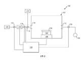
100:設備100: Equipment
102:反應腔室102: Reaction Chamber
104:基板104: Substrate
106:暴露表面106: Exposed Surfaces
108:基座108: Pedestal
110:入口端110: Entry port
112:出口端112: Exit port
114:沈積反應物源/反應物源114: Deposition reactant source/reactant source
116:反應物源閥116:Reactant source valve
118:第一閥118: The first valve
120:鈍化前驅物源120: Passivation precursor source
122:第二閥122: Second valve
124:載氣源124: carrier gas source
126:出口閥126: outlet valve
128:控制器/控制器組128: Controller/Controller Group
130:真空泵130: Vacuum pump
200:成簇工具200: Clustering Tool
202a:第一加工腔室202a: First processing chamber
202b:第二加工腔室202b: Second processing chamber
204:轉移腔室204: Transfer Chamber
206:裝載鎖定腔室206: Load lock chamber
208:冷卻台208: Cooling table
210:閘閥210: Gate valve
310:供應步驟310: Supply Steps
320:吸附步驟320: Adsorption step
330:冷卻步驟330: Cooling Step
340:供應步驟340: Supply Steps
350:產生步驟350: Generate Steps
410:供應步驟410: Supply Steps
420:吸附步驟420: Adsorption step
430:冷卻步驟430: Cooling Step
440:供應步驟440: Supply Steps
450:產生步驟450: Generate Steps
510:供應步驟510: Supply Steps
520:吸附步驟520: Adsorption step
530:移出步驟530: remove step
540:冷卻步驟540: Cooling Step
550:置放步驟550: Placement steps
560:供應步驟560: Supply Steps
570:產生步驟570: Generate Steps
610:暴露步驟610: Exposure Procedure
620:供應步驟620: Supply Steps
630:吸附步驟630: Adsorption step
640:冷卻步驟640: Cooling Step
650:暴露步驟650: Exposure Procedure
660:供應步驟660: Supply Steps
670:產生步驟670: Generate Steps
710:加熱步驟710: Heating step
720:供應步驟720: Supply Steps
730:吸附步驟730: Adsorption step
740:冷卻步驟740: Cooling Step
750:再加熱步驟750: Reheat step
760:供應步驟760: Supply Steps
770:產生步驟770: Generation Step
810:供應步驟810: Supply Steps
820:吸附步驟820: Adsorption step
830:冷卻步驟830: Cooling Step
840:供應步驟840: Supply Steps
850:產生步驟850: Generation Step
860:選擇性沈積步驟860: Selective Deposition Step
圖1示意性繪示根據一些具體例的包含反應腔室之設備。Figure 1 schematically illustrates an apparatus including a reaction chamber, according to some embodiments.
圖2為根據一些具體例的包含反應腔室、轉移腔室及裝載鎖腔室之成簇工具的示意性平面視圖。2 is a schematic plan view of a cluster tool including a reaction chamber, a transfer chamber, and a load lock chamber, according to some embodiments.
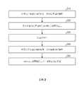
圖3為根據一些具體例的用於在基板之暴露表面上製備SAM之製程的流程圖。3 is a flow diagram of a process for fabricating a SAM on an exposed surface of a substrate, according to some embodiments.
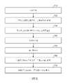
圖4為根據一些具體例用於在基板之暴露表面上製備SAM之製程的流程圖,在該製程中於沈積腔室內使該基板冷卻。4 is a flow diagram of a process for preparing a SAM on an exposed surface of a substrate during which the substrate is cooled within a deposition chamber, according to some embodiments.
圖5為根據一些具體例的用於在基板之暴露表面上製備SAM之製程的流程圖,在該製程中於沈積腔室外部使該基板冷卻。5 is a flow diagram of a process for preparing a SAM on an exposed surface of a substrate in which the substrate is cooled outside a deposition chamber, according to some embodiments.
圖6為根據一些具體例的用於在基板之暴露表面上製備SAM之製程的流程圖,該製程包括使基板之表面暴露於H2O中。6 is a flow diagram of a process for preparing a SAM on an exposed surface of a substrate that includes exposing the surface of the substrate toH2O , according to some embodiments.
圖7為根據一些具體例的用於在基板之暴露表面上製備SAM之製程的流程圖,在該製程中具有加熱、冷卻及再加熱溫度範圍。7 is a flow diagram of a process for fabricating a SAM on an exposed surface of a substrate with heating, cooling, and reheating temperature ranges in the process, according to some embodiments.
圖8為根據一些具體例的用於在第一暴露表面上製備SAM且隨後藉由氣相沈積將材料選擇性地沈積於第二暴露表面上之製程的流程圖。8 is a flow diagram of a process for preparing a SAM on a first exposed surface and then selectively depositing material on a second exposed surface by vapor deposition, according to some embodiments.
如在先前技術部分中所指出,存在使特定表面(例如反應器表面及經部分製造之積體電路結構的表面)針對氣相沈積(諸如ALD)而失活的製程,以允許在未經處理之表面上選擇性沈積。一種此類製程涉及在不需要膜沈積之暴露表面上方形成緻密填充之自組裝單層(self-assembled monolayer;SAM)。SAM為自氣相或液相前驅物自發地吸附(亦稱為以化學方式吸附)在表面上的相對有序之分子組裝體。典型SAM分子包括末端官能基、烴鏈及頭基。藉由在所選表面上方形成SAM,該SAM可藉由阻擋暴露表面上的否則將與彼等沈積前驅物反應之反應性位點來防止使用某些類型之氣相前驅物在該等暴露表面上方進行的膜生長。此類選擇性失活可尤其有效針對吸附驅動之製程,如ALD,但亦可阻礙某些類型之CVD。As noted in the prior art section, there are specific surfaces (eg, reactor surfaces and surfaces of partially fabricated integrated circuit structures) that are targeted for vapor deposition (such asALD) to allow selective deposition on untreated surfaces. One such process involves the formation of a densely packed self-assembled monolayer (SAM) over exposed surfaces that do not require film deposition. SAMs are relatively ordered molecular assemblies that are spontaneously adsorbed (also known as chemisorption) from gas-phase or liquid-phase precursors on a surface. Typical SAM molecules include terminal functional groups, hydrocarbon chains, and head groups. By forming a SAM over selected surfaces, the SAM can prevent the use of certain types of gas-phase precursors on exposed surfaces by blocking reactive sites on the exposed surfaces that would otherwise react with those deposition precursors Membrane growth performed above. Such selective inactivation can be particularly effective for adsorption-driven processes, such as ALD, but can also hinder certain types of CVD.
本申請案揭示用於基於氣相而沈積有機矽烷類之SAM的設備及製程,經由在後續暴露於SAM前驅物中之前對暴露於SAM前驅物中之基板使用中間冷卻(intermediate cooling),該等有機矽烷類之SAM可在暴露較少的情況下形成及/或花費更少時間,以便產生所期望的有機矽烷SAM。咸信中間冷卻允許第二SAM前驅物暴露以吸附至其中尚未吸附第一SAM前驅物之反應性位點上。在一些具體例中,中間物冷卻及第二SAM前驅物暴露之製程形成緻密且無針孔之SAM層,以使得其在長期暴露於在無SAM之其他表面上形成相對較厚層的後續選擇性沈積之後仍可抵抗成核。This application discloses apparatus and processes for vapor-phase based deposition of organosilane-based SAMs by using intermediate cooling of the substrate exposed to the SAM precursor prior to subsequent exposure to the SAM precursor, such as Organosilane-based SAMs can be formed with less exposure and/or take less time to produce the desired organosilane SAM. It is believed that the intercooling allows the exposure of the second SAM precursor for adsorption to reactive sites where the first SAM precursor has not been adsorbed. In some embodiments, the process of intermediate cooling and exposure of the second SAM precursor forms a dense and pinhole-free SAM layer, allowing it to be exposed to subsequent options for long-term exposure to form relatively thicker layers on other surfaces without SAM Resistant to nucleation after sexual deposition.
SAM前驅物可包括熟悉本技藝者已知的任何前驅物,諸如硫基類(thio-based)及有機矽烷類之SAM前驅物。在一些具體例中,SAM前驅物被識別於美國專利第7,914,847號,其揭示內容以全文引用之方式併入本文中。SAM前驅物分子可含具有各種碳鏈長度之烷基鏈取代基。有機矽烷類之SAM前驅物可包括例如下文所示之十八烷基(三(二甲基)胺基)矽烷。The SAM precursor may include any precursor known to those skilled in the art, such as thio-based and organosilane-based SAM precursors. In some embodiments, SAM precursors are identified in US Patent No. 7,914,847, the disclosure of which is incorporated herein by reference in its entirety. SAM precursor molecules can contain alkyl chain substituents of various carbon chain lengths. Organosilane-based SAM precursors may include, for example, octadecyl(tris(dimethyl)amino)silanes shown below.

SAM前驅物一般具有式R-Si-L3,其中L基團對應於活性基團,且R基團可為碳鏈或碳主鏈。在一些具體例中,活性基團可為烷胺基(例如-NMe2、-NEtMe、-NEt2)、烷氧基(例如-OMe、-OEt)或其混合物。在一些具體例中,活性基團可為可結合於基板之表面上的任何其他基團。在一些具體例中,SAM可含有之碳鏈長度或主鏈長度為1、2、3、5、10、15、18、20、25或30個碳原子、或介於此等值中之任一者之間的任何範圍、諸如1至25、2至20或3至18個碳原子。在一些具體例中,碳鏈可為烷基鏈。在一些具體例中,碳鏈可未經取代。在一些具體例中,碳鏈可經取代。術語經取代理解為意謂沿鏈之基團或原子由一或多個取代基取代。舉例而言,經取代之烷基鏈在沿碳鏈之任何位置處的一或多個氫原子可經諸如氟之取代基置換,其中沿碳鏈之位置包括碳鏈之末端以及末端之間的位置。在一些具體例中,碳鏈取代基可提供SAM層疏水性增加及/或水接觸角測量值增加。在一些具體例中,碳鏈可由一或多個氟基團取代。SAM precursors generally have the formulaR -Si-L3, where the L group corresponds to the reactive group, and the R group can be a carbon chain or carbon backbone. In some embodiments, the reactive group may be an alkylamino group (eg, -NMe2 , -NEtMe, -NEt2 ), an alkoxy group (eg, -OMe, -OEt), or a mixture thereof. In some embodiments, the reactive group can be any other group that can bind to the surface of the substrate. In some embodiments, the SAM may contain a carbon chain length or backbone length of 1, 2, 3, 5, 10, 15, 18, 20, 25, or 30 carbon atoms, or any value in between Any range in between, such as 1 to 25, 2 to 20, or 3 to 18 carbon atoms. In some embodiments, the carbon chain can be an alkyl chain. In some embodiments, the carbon chain can be unsubstituted. In some embodiments, the carbon chain can be substituted. The term substituted is understood to mean that a group or atom along the chain is substituted with one or more substituents. For example, a substituted alkyl chain can have one or more hydrogen atoms replaced with a substituent such as fluorine at any position along the carbon chain, where positions along the carbon chain include the ends of the carbon chain and the spaces between the ends Location. In some embodiments, carbon chain substituents can provide increased hydrophobicity of the SAM layer and/or increased water contact angle measurements. In some embodiments, the carbon chain can be substituted with one or more fluorine groups.
形成於暴露表面上方之SAM的完整性可藉由該表面之水接觸角(water contact angle;WCA)測量值來表徵。在一些具體例中,使用特定前驅物習知地形成之SAM的WCA為至多約108°。在一些具體例中,使用相同前驅物但用中間冷卻(intervening cooling)形成之SAM的WCA增加,諸如暴露表面之WCA為大於108°。在其他具體例中,用中間冷卻形成之SAM的WCA為大於約80°、大於約90°、大於約95°、大於約100°、大於約103°、大於約106°、大於約108°、大於約109°、大於約110°、大於約111°、大於約112°或大於約113°,或為介於此等值中之任一者之間的任何範圍,諸如約80°至約113°、約90°至約111°、約108°至約113°或約110°至約111°。The integrity of the SAM formed over an exposed surface can be characterized by the water contact angle (WCA) measurement of the surface. In some embodiments, the WCA of SAMs conventionally formed using certain precursors is at most about 108°. In some embodiments, the WCA of SAMs formed using the same precursor but with intervening cooling increased, such as the WCA of the exposed surface was greater than 108°. In other embodiments, the WCA of the SAM formed with intermediate cooling is greater than about 80°, greater than about 90°, greater than about 95°, greater than about 100°, greater than about 103°, greater than about 106°, greater than about 108°, greater than about 109°, greater than about 110°, greater than about 111°, greater than about 112°, or greater than about 113°, or any range between any of these values, such as about 80° to about 113° °, about 90° to about 111°, about 108° to about 113°, or about 110° to about 111°.
下文描述用於基於氣相而沈積有機矽烷類之SAM及選擇性氣相沈積的設備及製程的一些具體例。Some specific examples of equipment and processes for vapor-based deposition of organosilane-based SAMs and selective vapor deposition are described below.
圖1繪示根據一些具體例的包含反應腔室102之設備100,及其在已將基板104引入至反應腔室102中之後的特徵。反應腔室102可為CVD反應腔室、ALD反應腔室、經專門設計以用於SAM形成之腔室、或能夠在基板(諸如矽晶圓)上氣相沈積的任何其他類型之反應腔室。反應腔室102可為單基板加工機器或多基板加工機器。基板104可包括暴露表面106,其可經圖案化以包括例如暴露之絕緣及導電性表面。反應腔室102可包括基座108、入口端110、出口端112、沈積反應物源114(其可包括用於低蒸氣壓反應物之氣化器)、反應物源閥116、第一閥118、鈍化前驅物源120(其亦可包括氣化器)、第二閥122、載氣源124及出口閥126。出口閥126可與真空泵130流體連通。各種組件可為與控制器(或控制器組)128電子耦接。熟悉本技藝者應瞭解,僅示意性地顯示設備100,且其可採用多種其他配置且包括其他組件,諸如加熱器、容器、用於各種其他反應物之蒸發器或起泡器、用於溫度控制之控制系統、沈積前驅物之流量控制器、氣體分配系統等。1 illustrates an
在一些具體例中,SAM前驅物在鈍化前驅物源120中氣化。在一些具體例中,蒸氣源為處於約20℃、約40℃、約50℃、約70℃、約90℃、約100℃、約150℃、約200℃、約225℃、約250℃、約300℃、約400℃、或介於此等值中之任一者之間的任何範圍、諸如約20℃至約300℃、40℃至約250℃、50℃至約225℃、20℃至約400℃或約80℃至約400℃的溫度下。在其他具體例中,蒸氣源為處於約150℃至約400℃之溫度下。在再其他具體例中,蒸氣源為處於約200℃至約400℃之溫度下。在又再其他具體例中,蒸氣源為處於約150℃至約300℃之溫度下。熟悉技藝人士應瞭解,用於使SAM前驅物氣化而不使其熱分解的適合之溫度視所選前驅物而定。在一些具體例中,SAM形成可在氣化器及基座溫度各自單獨地設定成約20℃、約50℃、約100℃、約150℃、約185℃、約195℃、約200℃、約205℃、約250℃、約300℃、約350℃、約400℃、或介於此等值中之任一者之間的任何範圍、諸如約20℃至約400℃、約50℃至約300℃、約50℃至約250℃、約100℃至約200℃或約185℃至約205℃的情況下進行。下文所描述的藉由暴露於十八烷基(三(二甲基)胺基)矽烷中而形成SAM的實驗在氣化器及基座兩者溫度設定成介於185℃與205℃之間、更特定言之為約195℃的情況下進行。In some embodiments, the SAM precursor is vaporized in
基座108可用於以傳導方式加熱、冷卻或再加熱基板。在一些具體例中,控制器經程式化以將基座108維持在適合於吸附相關SAM之溫度下,該溫度可與上文對前驅物氣化所指出之範圍類似。在一些具體例中,控制器亦可經程式化以根據下文所描述之工序使基座108冷卻。The
雖然用基座108上之基板104來繪示,但應理解,鑒於下文揭示內容,在一些具體例中,其上形成鈍化層之基板可為反應腔室102本身之壁,以使得在形成鈍化層期間,期望於其未經鈍化之表面上後續沈積的基板104可不存在於腔室102。Although shown with the
雖然圖1顯示單獨反應物源114,在一些具體例中,設備100為專用SAM暴露反應器(SAM exposure reactor),以使得除鈍化前驅物源120中之SAM前驅物分子及載氣源124中諸如N2、He或Ar之惰性氣體以外,反應腔室102不連接至蒸氣源。Although FIG. 1 shows a
圖2為根據一些具體例之成簇工具200的示意性平面視圖,該成簇工具包含第一加工腔室202a、第二加工腔室202b、轉移腔室204及裝載鎖腔室206。腔室在其之間具有閘閥210,且轉移腔室204可包括轉移自動機。在一些具體例中,轉移腔室204可包含冷卻台208。熟悉本技藝者應瞭解,僅示意性地顯示成簇工具200,且其可採用多種其他配置且包括其他組件,諸如額外加工腔室、加熱器、蒸發器或起泡器、用於溫度控制之控制系統、沈積前驅物之流量控制器、氣體分配系統等。2 is a schematic plan view of a
在一些具體例中,成簇工具可包含多個反應腔室、轉移腔室及裝載鎖腔室。在一些具體例中,成簇工具環境可不包含轉移腔室。在一些具體例中,如下文所描述冷卻可在反應腔室中執行。在其他具體例中,冷卻可在轉移腔室中於冷卻台處執行。在再其他具體例中,冷卻可在裝載鎖腔室中執行。在再其他具體例中,冷卻可在成簇工具外部執行。在又再其他具體例中,冷卻可在成簇工具環境中之任何其他專用冷卻腔室或冷卻台中執行。在一些具體例中,冷卻可主動地執行,諸如使用空氣或惰性氣體(諸如氮氣、氦氣、氬氣或其混合物)以對流方式執行,或藉由將較冷元件移動至與基板或基座接近或接觸來以傳導方式執行。在採用對流冷卻台之具體例中,該冷卻台可僅用惰性氣體打入(plumb),而不連接至反應氣體。在一些具體例中,冷卻可藉由自熱源移出基板但不主動冷卻來被動地進行。在一些具體例中,在將SAM沈積於基板上之前,該等基板可儲存在冷卻腔室或冷卻台中。在一些具體例中,冷卻腔室或冷卻台可經配置以容納一個基板或可經配置以容納超過一個基板。在一些具體例中,冷卻腔室或冷卻台可經配置以容納1個或多個基板、2個或超過2個基板、3個或超過3個基板、5個或超過5個基板、10個或超過10個基板、15個或超過15個基板、或25個或超過25個基板、或介於此等值中之任一者之間的任何範圍。In some embodiments, the clustering tool can include multiple reaction chambers, transfer chambers, and load lock chambers. In some embodiments, the cluster tool environment may not include a transfer chamber. In some embodiments, cooling can be performed in the reaction chamber as described below. In other embodiments, cooling may be performed at a cooling station in a transfer chamber. In yet other embodiments, cooling may be performed in the load lock chamber. In still other embodiments, cooling may be performed external to the clustering tool. In yet other embodiments, cooling may be performed in any other dedicated cooling chamber or cooling stage in the cluster tool environment. In some embodiments, cooling can be performed actively, such as convectively using air or an inert gas such as nitrogen, helium, argon, or mixtures thereof, or by moving cooler components to and from the substrate or susceptor Approach or touch to perform conductively. In a specific example using a convection cooling stage, the cooling stage may only be plumb with an inert gas and not be connected to the reaction gas. In some embodiments, cooling can be passively performed by removing the substrate from the heat source without active cooling. In some specific cases, after sinking the SAMThe substrates can be stored in a cooling chamber or cooling stage before being deposited on the substrates. In some embodiments, the cooling chamber or cooling stage may be configured to accommodate one substrate or may be configured to accommodate more than one substrate. In some embodiments, the cooling chamber or cooling stage can be configured to accommodate 1 or more substrates, 2 or more substrates, 3 or more substrates, 5 or more substrates, 10 substrates Or more than 10 substrates, 15 or more substrates, or 25 or more substrates, or any range in between any of these values.
圖3為根據一些具體例的用於在基板之表面上製備SAM之方法的流程圖。該製程包含步驟310向基板之暴露表面供應第一SAM前驅物;藉此步驟320使初始SAM吸附在基板之暴露表面上;在步驟320吸附初始SAM之後,步驟330使基板冷卻;在步驟330冷卻之後,步驟340向基板之暴露表面供應第二SAM前驅物;藉此步驟350在基板之暴露表面上產生補充SAM。3 is a flow diagram of a method for fabricating a SAM on a surface of a substrate according to some embodiments. The process includes step 310 supplying a first SAM precursor to the exposed surface of the substrate; whereby
在一些具體例中,供應第一SAM前驅物可包含約0.1秒至約30分鐘之SAM前驅物暴露脈衝。在其他具體例中,供應第一SAM前驅物可包含約0.5秒至約30秒之SAM前驅物暴露脈衝。在再其他具體例中,供應第一SAM前驅物可包含約1秒至約10秒之SAM前驅物暴露脈衝。在一些具體例中,供應第一SAM前驅物可另外包含約10秒至約30分鐘之SAM前驅物浸泡,其中暴露浸泡包含使基板繼續暴露於SAM前驅物中,且可包括密封加工腔室之出口以將SAM前驅物截留在加工腔室中。在其他具體例中,供應第一SAM前驅物可另外包含約0.5分鐘至約15分鐘之SAM前驅物浸泡。在再其他具體例中,供應第一SAM前驅物可包含約1分鐘至約10分鐘之SAM前驅物暴露浸泡。流動速率將視SAM形成條件及腔室大小而定。舉例而言,對於用於300mm晶圓之單基板加工腔室,供應第一SAM前驅物可包含約50sccm至約1600sccm之SAM前驅物流動速率。在下文所描述之實驗中,供應第一SAM前驅物包含約800sccm之SAM前驅物流動速率持續約5秒,後接5分鐘浸泡。In some embodiments, supplying the first SAM precursor may comprise a SAM precursor exposure pulse of about 0.1 seconds to about 30 minutes. In other embodiments, supplying the first SAM precursor may include a SAM precursor exposure pulse of about 0.5 seconds to about 30 seconds. In still other embodiments, supplying the first SAM precursor may comprise a SAM precursor exposure pulse of about 1 second to about 10 seconds. In some embodiments, supplying the first SAM precursor may additionally include a SAM precursor soak for about 10 seconds to about 30 minutes, wherein the exposure soak includes continued exposure of the substrate to the SAM precursor, and may include sealing and addingThe outlet of the processing chamber to trap the SAM precursor in the processing chamber. In other embodiments, supplying the first SAM precursor may additionally include a soaking of the SAM precursor for about 0.5 minutes to about 15 minutes. In still other embodiments, supplying the first SAM precursor may include a SAM precursor exposure soak for about 1 minute to about 10 minutes. The flow rate will depend on the SAM formation conditions and the size of the chamber. For example, for a single substrate processing chamber for a 300 mm wafer, supplying the first SAM precursor may comprise a SAM precursor flow rate of about 50 seem to about 1600 seem. In the experiments described below, the first SAM precursor was supplied comprising a SAM precursor flow rate of about 800 seem for about 5 seconds followed by a 5 minute soak.
在一些具體例中,冷卻可使用空氣或環境氣氛以對流方式執行。在其他具體例中,冷卻可使用惰性氣體,例如氮氣以對流方式執行。在再其他具體例中,冷卻可藉由使基座108或用於基板104之其他支架主動冷卻來以傳導方式執行。在再其他具體例中,冷卻可藉由自在鈍化前驅物暴露期間所用之熱源移出基板來被動地執行,且可涉及將基板置放台上或僅用轉移自動機固持基板直至足夠冷卻為止。在一些具體例中,可執行冷卻持續約1秒、約5秒、約10秒、約60秒、約300秒、約600秒、約1分鐘、約5分鐘、約15分鐘、約30分鐘、約60分鐘或約24小時、或介於此等值中之任一者之間的任何範圍、諸如約1秒至約600秒、約5秒至約300秒、約10秒至約60秒、約1分鐘至約30分鐘或約1分鐘至約15分鐘。在一些具體例中,可執行冷卻持續少於10秒、少於30秒、少於60秒、少於5分鐘、少於10分鐘、少於15分鐘、少於30分鐘或少於60分鐘。在一些具體例中,可執行冷卻持續約1分鐘至約60分鐘。在一些具體例中,可執行冷卻持續約6小時至約24小時。鼓風冷卻或快速冷卻可指約60秒或少於60秒之冷卻時間。普通冷卻可指約60秒或超過60秒、諸如約1分鐘至約30分鐘之冷卻時間。In some embodiments, cooling may be performed in a convective manner using air or ambient atmosphere. In other embodiments, cooling may be performed in a convection manner using an inert gas, such as nitrogen. In still other embodiments, cooling may be performed conductively by actively cooling the
在一些具體例中,執行冷卻直至小於或處於約100℃、小於或處於約75℃、小於或處於約50℃、小於或處於約30℃、小於或處於約25℃、小於或處於約20℃、小於或處於約15℃。在一些具體例中,執行冷卻直至約0℃至約50℃。在一些具體例中,執行冷卻直至約15℃至約30℃。在再其他具體例中,執行冷卻直至約20℃至約25℃。在又再其他具體例中,執行冷卻直至約20℃或室溫。在採用主動或鼓風冷卻之一些具體例中,最終冷卻溫度可低於冰點,處於約0℃或小於0℃、處於約-10℃或小於-10℃、處於約-25℃或小於-25℃、處於約-50℃或小於-50℃、處於約-80℃或小於-80℃、處於約-100℃或小於-100℃、處於約-200℃或小於-200℃、或介於此等值中之任一者之間的任何範圍。在一些具體例中,執行冷卻直至低於SAM形成溫度之最終溫度。在一些具體例中,執行冷卻直至低於SAM形成溫度約50℃或超過50℃、約100℃或超過100℃、約125℃或超過125℃、約150℃或超過150℃、或約175℃或超過175℃、或介於此等值中之任一者之間的任何範圍的溫度。在一些具體例中,執行冷卻直至比SAM形成溫度小約75%(如以攝氏度為單位所測量)、比SAM形成溫度小約50%、比SAM形成溫度小約35%、比SAM形成溫度小約20%、比SAM形成溫度小約15%、比SAM形成溫度小約10%、或介於此等值中之任一者之間的任何範圍。In some embodiments, cooling is performed until less than or at about 100°C, less than or at about 75°C, less than or at about 50°C, less than or at about 30°C, less than or at about 25°C, less than or at about 20°C , less than or at about 15°C. In some embodiments, cooling is performed until about 0°C to about 50°C. In some embodiments, cooling is performed until about 15°C to about 30°C. In yet other specific examples, cooling is performed until about 20°C to about 25°C. In yet other embodiments, cooling is performed up to about 20°C or room temperature. In some embodiments employing active or blast cooling, the final cooling temperature may be below freezing, at about 0°C or less, at about -10°C or less than -10°C, at about -25°C or less than -25°C °C, at about -50 °C or less than -50 °C, at about -80 °C or less than -80 °C, at about -100 °C or less than -100 °C, at about -200 °C or less than -200 °C, or in between Any range between any of the equivalent values. In some embodiments, cooling is performed to a final temperature below the SAM formation temperature. In some embodiments, cooling is performed until about 50°C or more, about 100°C or more, about 125°C or more, about 150°C or more, or about 175°C below the SAM formation temperature or temperatures in excess of 175°C, or any range between any of these values. In some embodiments, cooling is performed until about 75% less than the SAM formation temperature (as measured in degrees Celsius), about 50% less than the SAM formation temperature, less than the SAM formation temperatureabout 35% less than the SAM forming temperature, about 20% less than the SAM forming temperature, about 15% less than the SAM forming temperature, about 10% less than the SAM forming temperature, or any range between any of these values .
在一些具體例中,冷卻至合乎期望之溫度可在一個步驟中執行。在一些具體例中,冷卻至合乎期望之溫度可在超過一個步驟中執行,其中可將基板冷卻至一或多個中間溫度,且接著隨後冷卻至最終合乎期望之溫度。在一些具體例中,一或多個中間冷卻步驟可執行冷卻達到低於SAM形成溫度之中間溫度。在一些具體例中,中間冷卻溫度低於SAM形成溫度約20℃或超過20℃、約50℃或超過50℃、約75℃或超過75℃、或約100℃或超過100℃、或介於此等值中之任一者之間的任何範圍。在一些具體例中,中間冷卻溫度比SAM形成溫度小約15%(如以攝氏度為單位所測量)、比SAM形成溫度小約25%、比SAM形成溫度小約30%、比SAM形成溫度小約40%、比SAM形成溫度小約50%、比SAM形成溫度小約60%、比SAM形成溫度小約70%、比SAM形成溫度小約80%、比SAM形成溫度小約90%、或介於此等值中之任一者之間的任何範圍諸如15%至90%、25%至70%或30%至60%。In some embodiments, cooling to the desired temperature can be performed in one step. In some embodiments, cooling to the desired temperature may be performed in more than one step, wherein the substrate may be cooled to one or more intermediate temperatures, and then subsequently cooled to the final desired temperature. In some embodiments, one or more intermediate cooling steps may perform cooling to an intermediate temperature below the SAM formation temperature. In some embodiments, the intermediate cooling temperature is about 20°C or more, about 50°C or more, about 75°C or more, or about 100°C or more, or between Any range between any of these values. In some embodiments, the intercooling temperature is about 15% less than the SAM formation temperature (as measured in degrees Celsius), about 25% less than the SAM formation temperature, about 30% less than the SAM formation temperature, less than the SAM formation temperature about 40% less, about 50% less than the SAM formation temperature, about 60% less than the SAM forming temperature, about 70% less than the SAM forming temperature, about 80% less than the SAM forming temperature, about 90% less than the SAM forming temperature, or Any range between any of these values such as 15% to 90%, 25% to 70%, or 30% to 60%.
在一些具體例中,供應第二SAM前驅物可包含使基板暴露於SAM前驅物中持續約0.1秒至約30分鐘。在其他具體例中,供應第二SAM前驅物可包含使基板暴露於SAM前驅物中持續約0.5秒至約20秒。在再其他具體例中,供應第二SAM前驅物可包含約1秒至約10秒之SAM前驅物暴露。在一些具體例中,供應第二SAM前驅物可另外包含約10秒至約30分鐘之SAM前驅物浸泡,其中浸泡包含使基板繼續暴露於SAM前驅物中,且可包括密封加工腔室之出口以將SAM前驅物截留在加工腔室中。在其他具體例中,供應第二SAM前驅物可包含約0.5分鐘至約15分鐘之SAM前驅物浸泡。在再其他具體例中,供應第二SAM前驅物可包含約1分鐘至約10分鐘之SAM前驅物浸泡。流動速率將視SAM形成條件及腔室大小而定。舉例而言,對於用於300mm晶圓之單基板加工腔室,供應第二SAM前驅物可包含約50sccm至約1600sccm之SAM前驅物流動速率。在下文所描述之實驗中,供應第二SAM前驅物包含約800sccm之SAM前驅物流動速率持續約5秒,後接5分鐘浸泡。In some embodiments, supplying the second SAM precursor can include exposing the substrate to the SAM precursor for about 0.1 seconds to about 30 minutes. In other embodiments, supplying the second SAM precursor may include exposing the substrate to the SAM precursor for about 0.5 seconds to about 20 seconds. In still other embodiments, supplying the second SAM precursor can include about 1 second to about 10 seconds of SAM precursor exposure. In some specific instances, supplyThe second SAM precursor may additionally include a SAM precursor soak for about 10 seconds to about 30 minutes, wherein the soak includes continued exposure of the substrate to the SAM precursor, and may include sealing the outlet of the processing chamber to trap the SAM precursor in the SAM precursor in the processing chamber. In other embodiments, supplying the second SAM precursor may include soaking the SAM precursor for about 0.5 minutes to about 15 minutes. In still other embodiments, supplying the second SAM precursor may include about 1 minute to about 10 minutes of soaking with the SAM precursor. The flow rate will depend on the SAM formation conditions and the size of the chamber. For example, for a single substrate processing chamber for 300 mm wafers, supplying the second SAM precursor may include a SAM precursor flow rate of about 50 seem to about 1600 seem. In the experiments described below, the second SAM precursor was supplied comprising a SAM precursor flow rate of about 800 seem for about 5 seconds followed by a 5 minute soak.
在一些具體例中,用於在基板之表面上製備SAM的製程包含一或多個額外循環之冷卻及暴露於第三SAM前驅物中。在一些具體例中,額外循環之冷卻及暴露於第三SAM前驅物中可在步驟330冷卻之後且在步驟340供應第二SAM前驅物之前執行。在一些具體例中,額外循環之冷卻及暴露於第三SAM前驅物中可在步驟340供應第二SAM前驅物之後執行。在一些具體例中,第三SAM前驅物可包含第一SAM前驅物、第二SAM前驅物、與第一SAM前驅物或第二SAM前驅物不同之SAM前驅物、或其混合物。In some embodiments, the process for preparing the SAM on the surface of the substrate includes one or more additional cycles of cooling and exposure to a third SAM precursor. In some embodiments, additional cycles of cooling and exposure to the third SAM precursor may be performed after
一般熟悉本技藝者應理解,第一SAM前驅物及第二SAM前驅物暴露可在於本說明書通篇中所描述之任何蒸氣源溫度下獨立地執行。一般熟悉本技藝者應理解,第一SAM前驅物及第二SAM前驅物可具有相同組成。在下文所描述之實驗中,第一SAM前驅物及第二SAM前驅物兩者皆包含十八烷基(三(二甲基)胺基)矽烷。第一SAM前驅物及第二SAM前驅物暴露可在不同加工腔室中執行,但將更常在同一加工腔室中進行,尤其當對兩次暴露採用相同前驅物時。加工腔室可與用於後續選擇性ALD製程之加工腔室相同或不同。It will be understood by those of ordinary skill in the art that the exposure of the first SAM precursor and the second SAM precursor can be performed independently at any of the vapor source temperatures described throughout this specification. It will be understood by those of ordinary skill in the art that the first SAM precursor and the secondThe SAM precursors may have the same composition. In the experiments described below, both the first SAM precursor and the second SAM precursor included octadecyl(tris(dimethyl)amino)silane. The first and second SAM precursor exposures can be performed in different processing chambers, but will more often be performed in the same processing chamber, especially when the same precursor is used for both exposures. The processing chamber can be the same or different from the processing chamber used for the subsequent selective ALD process.
一般熟悉本技藝者亦應理解,第一SAM前驅物及第二SAM前驅物可具有不同組成。在一個具體例中,第一SAM前驅物可為長鏈分子,而第二SAM前驅物可為短鏈分子。在另一個具體例中,第一SAM前驅物可為短鏈分子,而第二SAM前驅物可為長鏈分子。在一些具體例中,碳原子數目對於長鏈分子大於或等於八個,而對於短鏈分子少於八個。在其他具體例中,碳原子數目對於長鏈分子大於或等於十二個。在其他具體例中,碳原子數目對於短鏈分子少於或等於六個。具有不同組成之SAM前驅物揭示於美國專利第7,914,847號及第8,293,658號中,其全部揭示內容出於所有目的以引用之方式併入本文中。It will also be understood by those of ordinary skill in the art that the first SAM precursor and the second SAM precursor may have different compositions. In a specific example, the first SAM precursor may be a long-chain molecule, and the second SAM precursor may be a short-chain molecule. In another specific example, the first SAM precursor may be a short-chain molecule, and the second SAM precursor may be a long-chain molecule. In some embodiments, the number of carbon atoms is greater than or equal to eight for long-chain molecules and less than eight for short-chain molecules. In other embodiments, the number of carbon atoms is greater than or equal to twelve for long chain molecules. In other embodiments, the number of carbon atoms is less than or equal to six for short chain molecules. SAM precursors with different compositions are disclosed in US Pat. Nos. 7,914,847 and 8,293,658, the entire disclosures of which are incorporated herein by reference for all purposes.
圖4為根據一些具體例的用於在基板之暴露表面上製備SAM之製程的流程圖,該製程包括在沈積腔室內對該基板進行中間冷卻。該製程包含步驟410在沈積腔室中向基板之暴露表面供應第一SAM前驅物;藉此步驟420使初始SAM吸附在基板之暴露表面上;隨後步驟430在沈積腔室內使基板冷卻;隨後步驟440向基板之暴露表面供應第二SAM前驅物;藉此步驟450在基板之暴露表面上產生補充SAM。圖4中所描述之製程與關於圖3所描述之製程類似,除了指定基板冷卻在沈積腔室內執行之外。在沈積腔室內使基板冷卻之方法可如上文所描述(例如藉由供應冷卻空氣或惰性氣體來以對流方式冷卻、使加工腔室中之基座主動傳導冷卻等)。4 is a flow diagram of a process for fabricating a SAM on an exposed surface of a substrate that includes intercooling the substrate within a deposition chamber, according to some embodiments. The process includes step 410 supplying a first SAM precursor to the exposed surface of the substrate in the deposition chamber; whereby
圖5為根據一些具體例的用於在基板之暴露表面上製備SAM之製程的流程圖,在該製程中於沈積腔室外部使該基板冷卻。該製程包含步驟510在沈積腔室中向基板之暴露表面供應第一SAM前驅物;藉此步驟520使初始SAM吸附在基板之暴露表面上;步驟530自沈積腔室移出基板;步驟540使基板冷卻;步驟550將基板置放至沈積腔室中;步驟560向基板之暴露表面供應第二SAM前驅物;藉此步驟570在基板之暴露表面上產生補充SAM。在一些具體例中,第一SAM前驅物及第二SAM前驅物為相同類型之前驅物。在一些具體例中,兩種前驅物在同一沈積腔室中供應。圖5中所描述之製程與關於圖3所描述之製程類似,除了指定基板冷卻在沈積腔室外部執行之外。在沈積腔室外部使基板冷卻之方法可類似於上文所描述(例如被動冷卻、對流冷卻、藉由與經主動冷卻之元件接觸或接近而傳導冷卻),且可在裝載鎖腔室、轉移腔室或另一個加工腔室中進行。5 is a flow diagram of a process for preparing a SAM on an exposed surface of a substrate in which the substrate is cooled outside a deposition chamber, according to some embodiments. The process includes
圖6為根據一些具體例的用於在基板之暴露表面上製備SAM之製程的流程圖,該製程包括使基板之表面暴露於H2O中。該製程包含步驟610使基板之表面暴露於H2O中;隨後620步驟向基板之暴露表面供應第一SAM前驅物;藉此步驟630使初始SAM吸附在基板之暴露表面上;隨後步驟640使基板冷卻;步驟650使基板之表面暴露於H2O中;隨後步驟660向基板之暴露表面供應第二SAM前驅物;藉此步驟670在基板之暴露表面上產生補充SAM。圖6中所描述之製程與關於圖3所描述之製程類似,除了在每次供應SAM前驅物之前使基板之表面暴露於H2O中之外。應理解,術語「暴露表面」描述基板上與圖3-5中所描述相同之表面,即使該表面經H2O或任何其他中間處理來處理。在一些具體例中,在供應第一SAM前驅物之前使基板之表面暴露於H2O中,但不在供應第二SAM前驅物之前使基板之表面暴露於H2O中。在其他具體例中,在供應第二SAM前驅物之前使基板之表面暴露於H2O中,但不在供應第一SAM前驅物之前使基板之表面暴露於H2O中。如上文所指出,第一SAM前驅物及第二SAM前驅物可具有相同組成。冷卻可在沈積腔室內或外部(例如在裝載鎖腔室內、在轉移腔室中或在另一個加工腔室中)進行。在一些具體例中,使基板之表面暴露於H2O持續約0.1秒至約10秒。使基板之表面暴露於H2O持續約0.25秒至約5秒。在下文所描述之實驗中,使基板之表面暴露於H2O持續約1秒。6 is a flow diagram of a process for preparing a SAM on an exposed surface of a substrate that includes exposing the surface of the substrate toH2O , according to some embodiments. The process includes step 610 exposing the surface of the substrate toH2O ; then step 620 supplying a first SAM precursor to the exposed surface of the substrate; whereby
圖7為用於在基板之暴露表面上製備SAM之製程的流程圖。製程包含步驟710供應基板且將其加熱至適合於SAM形成之溫度;步驟720向基板之暴露表面供應第一SAM前驅物;藉此步驟730使初始SAM吸附在基板之暴露表面上;隨後步驟740使基板冷卻以促進後續SAM補充;步驟750再加熱基板;隨後步驟760向基板之暴露表面供應第二SAM前驅物;藉此步驟770在基板之暴露表面上產生補充SAM。圖7中所描述之製程與關於圖3所描述之製程類似,除了指定在冷卻之前及之後加熱及再加熱基板之外。如上文所指出,第一SAM前驅物及第二SAM前驅物可具有相同組成。各階段之溫度範圍可如上文所提及。在一些具體例中,基板使用加工腔室中之基座來加熱。基座及基板可以輻射、電阻或電感方式加熱。使基板冷卻之方法可如上文所描述,亦即,在沈積腔室內或外部(例如在裝載鎖腔室內、在轉移腔室中或在另一個加工腔室)中冷卻。7 is a flow diagram of a process for preparing a SAM on an exposed surface of a substrate. The process includes step 710 supplying the substrate and heating it to a temperature suitable for SAM formation; step 720 supplying a first SAM precursor to the exposed surface of the substrate; whereby
在一些具體例中,在如上文所描述形成SAM後,藉由氣相沈積製程使諸如金屬性材料(例如元素金屬、金屬氧化物、金屬氮化物、金屬合金等)之材料相對於第一表面選擇性地沈積於第二表面上,其中該第一表面包含藉由本文所描述之製程形成的SAM。在一些具體例中,第一表面為絕緣表面。在其他具體例中,第一表面為導電性表面。在一些具體例中,第一表面為積體電路結構之表面,諸如半導體基板上之表面。在一些具體例中,反應物包括第一疏水性反應物及第二反應物。可選擇第一疏水性反應物及第二反應物以使合乎期望之材料沈積。在一些具體例中可利用額外反應物(第三反應物、第四反應物等)以例如向所沈積之材料中提供額外組分。在一些具體例中,第二表面對一或多種氣相反應物實質上具反應性,而第一表面實質上不具反應性。In some embodiments, after forming the SAM as described above, a material such as a metallic material (eg, elemental metal, metal oxide, metal nitride, metal alloy, etc.) is affixed to the first surface by a vapor deposition process is selectively deposited on a second surface, wherein the first surface includes a SAM formed by the processes described herein. In some embodiments, the first surface is an insulating surface. In another specific example, the first surface is a conductive surface. In some embodiments, the first surface is a surface of an integrated circuit structure, such as a surface on a semiconductor substrate. In some embodiments, the reactants include a first hydrophobic reactant and a second reactant. The first hydrophobic reactant and the second reactant can be selected to deposit the desired material. Additional reactants (third reactants, fourth reactants, etc.) may be utilized in some embodiments, eg, to the deposited materialAdditional components are provided. In some embodiments, the second surface is substantially reactive to one or more gas-phase reactants, and the first surface is substantially non-reactive.
在一些具體例中,氣相沈積製程為ALD型製程,其中至少一種反應物在自限性過程中在很大程度上完整吸附。在一些具體例中,沈積製程可為氣相沈積製程,其中至少一種反應物至少部分地分解,諸如在第一表面上選擇性地分解。舉例而言,在一些具體例中,氣相沈積製程可為化學氣相沈積(chemical vapor deposition;CVD)製程,諸如依序或循環CVD製程或單源CVD製程。In some embodiments, the vapor deposition process is an ALD-type process in which at least one reactant is largely completely adsorbed in a self-limiting process. In some embodiments, the deposition process may be a vapor deposition process in which the at least one reactant is at least partially decomposed, such as selectively on the first surface. For example, in some embodiments, the vapor deposition process may be a chemical vapor deposition (CVD) process, such as a sequential or cyclic CVD process or a single source CVD process.
圖8為用於在第一暴露表面上製備SAM且隨後藉由氣相沈積將材料選擇性地沈積於第二暴露表面上之製程的流程圖。該製程包含步驟810向第一暴露表面供應第一SAM前驅物;藉此步驟820使初始SAM吸附在第一暴露表面上;隨後步驟830使基板冷卻;隨後步驟840向第一暴露表面供應第二SAM前驅物;藉此步驟850在第一暴露表面產生補充SAM;及隨後步驟860相對於沈積於其上具有補充SAM之第一暴露表面上,藉由氣相沈積將材料選擇性地沈積於第二暴露表面上。圖8中所描述之製程與關於圖3所描述之製程類似,除了指定隨後相對於沈積於第一暴露表面上,將材料選擇性地沈積於第二表面上。選擇性沈積於多種暴露表面上之方法可類似於上文所描述。步驟860選擇性沈積可在與步驟810/840其中供應SAM之腔室相同或不同的沈積腔室中進行。舉例而言,參看圖2,使用第一SAM前驅物及第二SAM前驅物暴露形成SAM可在第一加工腔室202a中進行,而選擇性沈積在第二加工腔室202b中執行。在另一個實施例中,使用第一SAM前驅物暴露形成初始SAM可在第一加工腔室202a中進行,而使用第二SAM前驅物暴露形成補充SAM可在第二加工腔室202b中進行,且選擇性沈積在第三加工腔室中執行。8 is a flow diagram of a process for preparing a SAM on a first exposed surface and then selectively depositing material on a second exposed surface by vapor deposition. The process includes step 810 supplying a first SAM precursor to the first exposed surface; whereby a
本文所描述之SAM形成可具選擇性。舉例而言,SAM可自然吸附在一些類型之表面上而不吸附在其他化學或形態不同之表面上。此外,後續沈積可具選擇性,如上文關於圖8中步驟860之選擇性沈積所描述。The SAM formation described herein can be selective. For example, SAM can naturally adsorb on some types of surfaces but not on other chemically or morphologically different surfaces. Furthermore, subsequent depositions can be selective, as described above with respect to the selective deposition of step 860 in FIG. 8 .
在一些具體例中,將材料相對於不同第一表面選擇性地沈積於第二基板表面上。選擇性可以藉由[(於第二表面上之沈積)-(於第一表面上之沈積)]/(於第二表面上之沈積)所計算的百分比形式給出。沈積可以多種方式中之任一者加以測量。在一些具體例中,沈積可以沈積材料之厚度的測量值形式給出。在一些具體例中,沈積可以沈積材料之量的測量值形式給出。In some embodiments, the material is selectively deposited on the second substrate surface relative to a different first surface. Selectivity can be given as a percentage calculated as [(deposition on second surface)-(deposition on first surface)]/(deposition on second surface). Deposition can be measured in any of a number of ways. In some embodiments, the deposition may be given as a measurement of the thickness of the deposited material. In some embodiments, deposition may be given as a measure of the amount of material deposited.
在一些具體例中,選擇性為大於約10%、大於約50%、大於約75%、大於約85%、大於約90%、大於約93%、大於約95%、大於約98%、大於約99%或甚至大於約99.5%。在本文所描述之具體例中,選擇性可隨沈積之持續時間或厚度而變化。In some embodiments, the selectivity is greater than about 10%, greater than about 50%, greater than about 75%, greater than about 85%, greater than about 90%, greater than about 93%, greater than about 95%, greater than about 98%, greater than About 99% or even greater than about 99.5%. In the embodiments described herein, the selectivity can vary with the duration or thickness of the deposition.
在一些具體例中,相對於基板之第一表面沈積於基板之第二表面上具有至少約80%選擇性,其對於一些特定應用可為足夠選擇性。在一些具體例中,相對於基板之第二表面沈積於基板之第二表面上具有至少約50%選擇性,其對於一些特定應用可為足夠選擇性。在一些具體例中,相對於基板之第一表面沈積於基板之第二表面上具有至少約10%選擇性,其對於一些特定應用可為足夠選擇性。如本技藝中已知,部分選擇性沈積可後接短暫蝕刻,其可自不傾向之第一表面移除所有沈積材料,而將一些沈積材料留在所傾向之第二表面上。In some embodiments, the substrate is deposited on the substrate relative to the first surface of the substrate.There is at least about 80% selectivity on the second surface, which may be sufficiently selective for some specific applications. In some embodiments, the deposition on the second surface of the substrate is at least about 50% selective relative to the second surface of the substrate, which may be sufficiently selective for some specific applications. In some embodiments, the deposition on the second surface of the substrate is at least about 10% selective relative to the first surface of the substrate, which may be sufficiently selective for some specific applications. As is known in the art, a partial selective deposition can be followed by a brief etch that removes all of the deposited material from the unfavorable first surface, leaving some deposited material on the favored second surface.
在一些具體例中,沈積傾向於發生在第二表面,諸如金屬性表面、包含氧之金屬性表面或介電性表面上,且不傾向於第一表面,諸如有機表面(例如本文所描述之SAM)上。在一些具體例中,第一表面及第二表面可為同一基板之表面(例如同一晶圓或加工腔室之表面)。在其他具體例中,第一表面及第二表面可為不同基板之表面(例如晶圓之表面及加工腔室之表面,或反之亦然)。In some embodiments, deposition tends to occur on a second surface, such as a metallic surface, a metallic surface containing oxygen, or a dielectric surface, and not on a first surface, such as an organic surface (eg, as described herein). SAM). In some embodiments, the first surface and the second surface may be surfaces of the same substrate (eg, surfaces of the same wafer or processing chamber). In other embodiments, the first surface and the second surface may be surfaces of different substrates (eg, a surface of a wafer and a surface of a processing chamber, or vice versa).
實施例1-10在冷卻之前及之後使用十八烷基(三(二甲基)胺基)矽烷(CH3(CH2)17Si(N(CH3)2)3)作為SAM前驅物來執行。「1個循環」意謂5秒SAM前驅物脈衝後接5分鐘浸泡。「使用H2O之1個循環」意謂1秒H2O脈衝後接5秒SAM前驅物脈衝後接5分鐘浸泡。SAM使用195℃之基板溫度、195℃之蒸氣源溫度及800sccm之前驅物流動速率來製備。測量所得SAM之水接觸角(water contact angle;WCA)。Examples 1-10 using octadecyl(tris(dimethyl)amino)silane (CH3 (CH2 )17Si (N(CH3 )2 )3 ) as SAM precursor before and after cooling implement. "1 cycle" means a 5 second SAM precursor pulse followed by a 5 minute soak. "1 cycle withH2O " means a 1 secondH2O pulse followed by a 5 second SAM precursor pulse followed by a 5 minute soak. SAMs were prepared using a substrate temperature of 195°C, a vapor source temperature of 195°C, and a precursor flow rate of 800 seem. The water contact angle (WCA) of the obtained SAM was measured.

如可見,若不存在冷卻,則SAM前驅物之循環數目及供應或不供應H2O對WCA影響極小。另一方面,冷卻可對WCA影響顯著。在上文圖表中,「透氣(air break)」表示因為將基板自熱基座移出送至其可容易冷卻之環境中而進行的冷卻步驟。由於在裝載鎖中維持之低壓力減緩冷卻速率,故將基板移出送至裝載鎖中持續30分鐘可不引起顯著冷卻,而將基板留在裝載鎖中持續隔夜使基板足夠冷卻以引起高WCA。As can be seen, if cooling is not present, the number of cycles of the SAM precursor and the supply or absence ofH2O has little effect on the WCA. On the other hand, cooling can have a significant impact on WCA. In the above diagram, "air break" refers to the cooling step that occurs as the substrate is moved out of the thermal base to an environment where it can be easily cooled. Since the low pressure maintained in the load lock slows the cooling rate, moving the substrate out of the load lock for 30 minutes may not cause significant cooling, while leaving the substrate in the load lock overnight allows the substrate to cool enough to cause a high WCA.
對熟悉本技藝者將顯而易見的是,在不背離本發明之範疇或精神的情況下,可在本發明中進行各種修改及變化。因此,意欲本發明涵蓋本發明之修改及變化,其限制條件為其在所附申請專利範圍及其等效物範疇內出現。It will be apparent to those skilled in the art that various modifications and variations can be made in the present invention without departing from the scope or spirit of the inventions. Therefore, it is intended that this invention covers modifications and variations of this invention, subject to the limitations that come within the scope of the appended claims and their equivalents.
310:供應步驟310: Supply Steps
320:吸附步驟320: Adsorption step
330:冷卻步驟330: Cooling Step
340:供應步驟340: Supply Steps
350:產生步驟350: Generate Steps
Claims (23)
Translated fromChineseApplications Claiming Priority (2)
| Application Number | Priority Date | Filing Date | Title |
|---|---|---|---|
| US201762532515P | 2017-07-14 | 2017-07-14 | |
| US62/532,515 | 2017-07-14 |
Publications (2)
| Publication Number | Publication Date |
|---|---|
| TW201918579A TW201918579A (en) | 2019-05-16 |
| TWI772459Btrue TWI772459B (en) | 2022-08-01 |
Family
ID=64999829
Family Applications (3)
| Application Number | Title | Priority Date | Filing Date |
|---|---|---|---|
| TW112116315ATWI810141B (en) | 2017-07-14 | 2018-07-12 | Apparatus for depositing self-assembled monolayer on substrate and method of self-assembled monolayer formation and selective deposition |
| TW111124307ATWI804369B (en) | 2017-07-14 | 2018-07-12 | Apparatus for depositing self-assembled monolayer on surface of substrate |
| TW107124150ATWI772459B (en) | 2017-07-14 | 2018-07-12 | Methods for preparing self-assembled monolayers |
Family Applications Before (2)
| Application Number | Title | Priority Date | Filing Date |
|---|---|---|---|
| TW112116315ATWI810141B (en) | 2017-07-14 | 2018-07-12 | Apparatus for depositing self-assembled monolayer on substrate and method of self-assembled monolayer formation and selective deposition |
| TW111124307ATWI804369B (en) | 2017-07-14 | 2018-07-12 | Apparatus for depositing self-assembled monolayer on surface of substrate |
Country Status (3)
| Country | Link |
|---|---|
| US (3) | US10937645B2 (en) |
| KR (2) | KR102695000B1 (en) |
| TW (3) | TWI810141B (en) |
Families Citing this family (7)
| Publication number | Priority date | Publication date | Assignee | Title |
|---|---|---|---|---|
| TWI810141B (en) | 2017-07-14 | 2023-07-21 | 荷蘭商Asm Ip私人控股有限公司 | Apparatus for depositing self-assembled monolayer on substrate and method of self-assembled monolayer formation and selective deposition |
| US20190316256A1 (en)* | 2018-04-13 | 2019-10-17 | Applied Materials, Inc. | Methods Of Selective Atomic Layer Deposition |
| JP7262354B2 (en)* | 2019-09-24 | 2023-04-21 | 東京エレクトロン株式会社 | Deposition method |
| JP7353200B2 (en)* | 2020-02-06 | 2023-09-29 | 東京エレクトロン株式会社 | Film forming method |
| CN113838744A (en) | 2020-06-24 | 2021-12-24 | Asm Ip私人控股有限公司 | Regioselective organic material removal |
| US20230212747A1 (en)* | 2021-12-31 | 2023-07-06 | Applied Materials, Inc. | Apparatus and Methods for Self-Assembled Monolayer (SAM) Deposition in Semiconductor Equipment |
| WO2025038645A1 (en)* | 2023-08-14 | 2025-02-20 | Applied Materials, Inc. | Method for employing stable self-assembled monolayers as release layers for lithium deposition and transfer onto a receiving substrate |
Citations (2)
| Publication number | Priority date | Publication date | Assignee | Title |
|---|---|---|---|---|
| US20110198736A1 (en)* | 2010-02-17 | 2011-08-18 | Asm America, Inc. | Reactive site deactivation against vapor deposition |
| TWI394862B (en)* | 2003-05-09 | 2013-05-01 | Asm Inc | Reactor surface passivation through chemical deactivation |
Family Cites Families (15)
| Publication number | Priority date | Publication date | Assignee | Title |
|---|---|---|---|---|
| US6073366A (en)* | 1997-07-11 | 2000-06-13 | Asm America, Inc. | Substrate cooling system and method |
| US7914847B2 (en) | 2003-05-09 | 2011-03-29 | Asm America, Inc. | Reactor surface passivation through chemical deactivation |
| WO2009135686A2 (en)* | 2008-05-09 | 2009-11-12 | Amf Gmbh | Self-assembled monolayers and method of production |
| CN104091777B (en)* | 2009-11-17 | 2017-09-12 | 伊帆科技股份有限公司 | Equipment for handling base material |
| US8562750B2 (en) | 2009-12-17 | 2013-10-22 | Lam Research Corporation | Method and apparatus for processing bevel edge |
| US9112003B2 (en) | 2011-12-09 | 2015-08-18 | Asm International N.V. | Selective formation of metallic films on metallic surfaces |
| TW201326444A (en)* | 2011-12-28 | 2013-07-01 | Pinecone Material Inc | Thin film deposition apparatus and using method of the same |
| JP2017503079A (en)* | 2014-01-05 | 2017-01-26 | アプライド マテリアルズ インコーポレイテッドApplied Materials,Incorporated | Film deposition using spatial atomic layer deposition or pulsed chemical vapor deposition |
| TWI661072B (en) | 2014-02-04 | 2019-06-01 | 荷蘭商Asm Ip控股公司 | Selective deposition of metals, metal oxides, and dielectrics |
| US10047435B2 (en) | 2014-04-16 | 2018-08-14 | Asm Ip Holding B.V. | Dual selective deposition |
| US9490145B2 (en) | 2015-02-23 | 2016-11-08 | Asm Ip Holding B.V. | Removal of surface passivation |
| EP3424070B1 (en)* | 2016-03-03 | 2024-03-27 | Applied Materials, Inc. | Improved self-assembled monolayer blocking with intermittent air-water exposure |
| US9803277B1 (en) | 2016-06-08 | 2017-10-31 | Asm Ip Holding B.V. | Reaction chamber passivation and selective deposition of metallic films |
| US9911595B1 (en) | 2017-03-17 | 2018-03-06 | Lam Research Corporation | Selective growth of silicon nitride |
| TWI810141B (en) | 2017-07-14 | 2023-07-21 | 荷蘭商Asm Ip私人控股有限公司 | Apparatus for depositing self-assembled monolayer on substrate and method of self-assembled monolayer formation and selective deposition |
- 2018
- 2018-07-12TWTW112116315Apatent/TWI810141B/enactive
- 2018-07-12TWTW111124307Apatent/TWI804369B/enactive
- 2018-07-12TWTW107124150Apatent/TWI772459B/enactive
- 2018-07-12USUS16/033,485patent/US10937645B2/enactiveActive
- 2018-07-13KRKR1020180081587Apatent/KR102695000B1/enactiveActive
- 2021
- 2021-01-15USUS17/150,153patent/US11495455B2/enactiveActive
- 2022
- 2022-09-23USUS17/934,725patent/US11749523B2/enactiveActive
- 2024
- 2024-08-08KRKR1020240105849Apatent/KR20240124268A/enactivePending
Patent Citations (2)
| Publication number | Priority date | Publication date | Assignee | Title |
|---|---|---|---|---|
| TWI394862B (en)* | 2003-05-09 | 2013-05-01 | Asm Inc | Reactor surface passivation through chemical deactivation |
| US20110198736A1 (en)* | 2010-02-17 | 2011-08-18 | Asm America, Inc. | Reactive site deactivation against vapor deposition |
Also Published As
| Publication number | Publication date |
|---|---|
| US11749523B2 (en) | 2023-09-05 |
| US11495455B2 (en) | 2022-11-08 |
| TW202332799A (en) | 2023-08-16 |
| KR20240124268A (en) | 2024-08-16 |
| TW202240015A (en) | 2022-10-16 |
| KR20190008143A (en) | 2019-01-23 |
| US20210134591A1 (en) | 2021-05-06 |
| US20190019674A1 (en) | 2019-01-17 |
| TWI804369B (en) | 2023-06-01 |
| US20230042093A1 (en) | 2023-02-09 |
| KR102695000B1 (en) | 2024-08-13 |
| US10937645B2 (en) | 2021-03-02 |
| TW201918579A (en) | 2019-05-16 |
| TWI810141B (en) | 2023-07-21 |
Similar Documents
| Publication | Publication Date | Title |
|---|---|---|
| TWI772459B (en) | Methods for preparing self-assembled monolayers | |
| JP7087031B2 (en) | Selective deposition of thin film dielectrics using surface blocking chemistry | |
| KR101202299B1 (en) | Method of manufacturing semiconductor device and substrate processing apparatus | |
| JP6999620B2 (en) | A method for producing a carbon-doped silicon oxide film and a silicon carbide film having a high carbon content. | |
| JP2009108402A (en) | In situ deposition of different metal-containing thin films using cyclopentadienyl metal precursor | |
| TW201938833A (en) | Compositions for depositing silicon nitride films and containers containing the same | |
| KR20150121217A (en) | LOW TEMPERATURE ATOMIC LAYER DEPOSITION OF FILMS COMPRISING SiCN OR SiCON | |
| WO2012012026A2 (en) | Metal film deposition | |
| KR20240134048A (en) | Methods for making silicon and nitrogen containing films | |
| JP2016500762A (en) | Method for producing silicon-containing thin film | |
| CN106068335A (en) | Germanium or the ald of germanium oxide | |
| EP1568075A2 (en) | Nitridation of high-k dielectrics | |
| JP2008211211A (en) | Semiconductor device manufacturing method and substrate processing apparatus | |
| TWI882336B (en) | Compositions and methods using same for carbon doped silicon containing films | |
| JP4979965B2 (en) | Substrate processing apparatus and semiconductor device manufacturing method | |
| TWI808951B (en) | Precursors for deposition of metal, metal nitride and metal oxide based films of transition metals | |
| TW201443274A (en) | Deposition of films using disiloxane precursors | |
| TWI883111B (en) | Methods of selectively forming metal-containing films | |
| JP5795520B2 (en) | Metal thin film material and metal thin film deposition method | |
| JP2025133137A (en) | Film forming method and film forming apparatus | |
| JP2024094581A (en) | Method for forming silicon oxide film | |
| JP2013104100A (en) | Method for depositing metallic thin film and raw material for depositing metallic thin film | |
| CN119343744A (en) | Single wafer reactor, low temperature thermal silicon nitride deposition | |
| WO2019030117A1 (en) | Ge-CONTAINING Co-FILM FORMING MATERIAL, Ge-CONTAINING Co FILM AND FILM FORMING METHOD THEREOF |