TWI771975B - Method for manufacturing anti-reflection layer of a solar panel - Google Patents
Method for manufacturing anti-reflection layer of a solar panelDownload PDFInfo
- Publication number
- TWI771975B TWI771975BTW110112166ATW110112166ATWI771975BTW I771975 BTWI771975 BTW I771975BTW 110112166 ATW110112166 ATW 110112166ATW 110112166 ATW110112166 ATW 110112166ATW I771975 BTWI771975 BTW I771975B
- Authority
- TW
- Taiwan
- Prior art keywords
- solar panel
- reflection layer
- layer
- manufacturing
- light guide
- Prior art date
Links
- 238000004519manufacturing processMethods0.000titleclaimsabstractdescription32
- 238000000034methodMethods0.000titleclaimsabstractdescription22
- 239000000463materialSubstances0.000claimsabstractdescription66
- 239000000758substrateSubstances0.000claimsabstractdescription37
- 238000007639printingMethods0.000claimsabstractdescription12
- 239000000853adhesiveSubstances0.000claimsabstractdescription10
- 230000001070adhesive effectEffects0.000claimsabstractdescription10
- 230000003287optical effectEffects0.000claimsdescription15
- -1polydimethylsiloxanePolymers0.000claimsdescription10
- 238000007650screen-printingMethods0.000claimsdescription10
- 239000003292glueSubstances0.000claimsdescription7
- 229920003229poly(methyl methacrylate)Polymers0.000claimsdescription7
- 239000004926polymethyl methacrylateSubstances0.000claimsdescription7
- 239000011347resinSubstances0.000claimsdescription6
- 229920005989resinPolymers0.000claimsdescription6
- 239000004793PolystyreneSubstances0.000claimsdescription5
- 239000004417polycarbonateSubstances0.000claimsdescription5
- WSSSPWUEQFSQQG-UHFFFAOYSA-N4-methyl-1-penteneChemical compoundCC(C)CC=CWSSSPWUEQFSQQG-UHFFFAOYSA-N0.000claimsdescription4
- 230000007423decreaseEffects0.000claimsdescription4
- 239000004205dimethyl polysiloxaneSubstances0.000claimsdescription4
- 229920000435poly(dimethylsiloxane)Polymers0.000claimsdescription4
- 229920000515polycarbonatePolymers0.000claimsdescription4
- 229920002223polystyrenePolymers0.000claimsdescription4
- COGLLVXIBJGDLH-UHFFFAOYSA-N2-(2-hydroxyethoxy)ethyl hydrogen carbonateChemical compoundOCCOCCOC(O)=OCOGLLVXIBJGDLH-UHFFFAOYSA-N0.000claims1
- 1250000039032-propenyl groupChemical group[H]C([*])([H])C([H])=C([H])[H]0.000claims1
- 230000000694effectsEffects0.000description9
- 239000000428dustSubstances0.000description7
- 238000010248power generationMethods0.000description5
- 238000002834transmittanceMethods0.000description4
- 230000008901benefitEffects0.000description3
- 230000008859changeEffects0.000description2
- 238000005516engineering processMethods0.000description2
- 238000010438heat treatmentMethods0.000description2
- 239000011116polymethylpenteneSubstances0.000description2
- 229920000306polymethylpentenePolymers0.000description2
- 230000008569processEffects0.000description2
- 238000010521absorption reactionMethods0.000description1
- NIXOWILDQLNWCW-UHFFFAOYSA-Nacrylic acid groupChemical groupC(C=C)(=O)ONIXOWILDQLNWCW-UHFFFAOYSA-N0.000description1
- 230000001464adherent effectEffects0.000description1
- 230000008033biological extinctionEffects0.000description1
- 239000011248coating agentSubstances0.000description1
- 238000000576coating methodMethods0.000description1
- 230000008878couplingEffects0.000description1
- 238000010168coupling processMethods0.000description1
- 238000005859coupling reactionMethods0.000description1
- LYCAIKOWRPUZTN-UHFFFAOYSA-Nethylene glycolNatural productsOCCOLYCAIKOWRPUZTN-UHFFFAOYSA-N0.000description1
- 239000011521glassSubstances0.000description1
- 238000009499grossingMethods0.000description1
- 230000003760hair shineEffects0.000description1
- WGCNASOHLSPBMP-UHFFFAOYSA-NhydroxyacetaldehydeNatural productsOCC=OWGCNASOHLSPBMP-UHFFFAOYSA-N0.000description1
- 238000005286illuminationMethods0.000description1
- 230000031700light absorptionEffects0.000description1
- 238000012986modificationMethods0.000description1
- 230000004048modificationEffects0.000description1
- 239000002245particleSubstances0.000description1
- 238000002360preparation methodMethods0.000description1
- 230000009467reductionEffects0.000description1
- 229910052594sapphireInorganic materials0.000description1
- 239000010980sapphireSubstances0.000description1
Images

Landscapes
- Laminated Bodies (AREA)
- Photovoltaic Devices (AREA)
Abstract
Description
Translated fromChinese本發明係關於一種抗反射層的製造方法,尤其是一種太陽能板抗反射層的製造方法。The present invention relates to a manufacturing method of an anti-reflection layer, in particular to a manufacturing method of an anti-reflection layer of a solar panel.
隨著再生能源的蓬勃發展,太陽能是目前再生能源當中具有發展潛力的項目之一。太陽光照射於太陽能板上,太陽光的光能被吸收而轉換為電能,因此,太陽能板的光能吸收量以及光線反射量,將直接影響太陽能板的發電效率。為了達到抗反射的效果,通常可以透過幾何光學的方式在太陽能板表面製備出金字塔型、半球體等微結構,藉此以減低光的耦合損失,進而提高光線捕捉率,並提升整體太陽能模組發電量。上述微結構的製備方式,通常需要先製作模具,再將高透明度之導光材料塗布於該模具,接著,使用加熱程序或光照程序使該導光材料固化而形成微結構,藉此以製作出具備抗光線反射能力的抗反射層。With the vigorous development of renewable energy, solar energy is one of the projects with development potential in the current renewable energy. When sunlight shines on the solar panel, the light energy of the sunlight is absorbed and converted into electrical energy. Therefore, the amount of light energy absorbed by the solar panel and the amount of light reflected will directly affect the power generation efficiency of the solar panel. In order to achieve the anti-reflection effect, microstructures such as pyramids and hemispheres can usually be prepared on the surface of the solar panel by geometric optics, thereby reducing the coupling loss of light, thereby improving the light capture rate and improving the overall solar module. power generation. The preparation method of the above-mentioned microstructure usually needs to make a mold first, then coat the light guide material with high transparency on the mold, and then use a heating process or an illumination process to cure the light guide material to form a microstructure, thereby making a Anti-reflection layer with anti-light reflection ability.
上述習知的太陽能板抗反射層,該微結構通常需要由精度極高的模具來進行翻模成型,而高精度模具的製程精密且繁複,因此,製作不易而且成本高昂。再者,該微結構會形成較粗糙的表面,且通常都直接裸露於大氣環境當中。雖然微結構能增加太陽能板的光吸收效率,但,微結構也容易附著粉塵、髒污,這些粉塵、髒污的顆粒通常具有較高的消光係數,因而造成光能損耗,或是造成漫反射現象,而使光能的利用率大幅度的下降,導致太陽能板的發電量降低。In the above-mentioned conventional solar panel anti-reflection layer, the microstructure usually needs to be overmolded by a mold with extremely high precision, and the manufacturing process of the high-precision mold is precise and complicated, so it is difficult to manufacture and the cost is high. Furthermore, the microstructures form a rougher surface and are usually directly exposed to the atmosphere. Although the microstructure can increase the light absorption efficiency of the solar panel, the microstructure is also easy to adhere to dust and dirt. These dust and dirt particles usually have a high extinction coefficient, thus causingThe loss of light energy, or the phenomenon of diffuse reflection, greatly reduces the utilization rate of light energy, resulting in a reduction in the power generation of the solar panel.
有鑑於此,習知的太陽能板抗反射層的製造方法確實仍有加以改善之必要。In view of this, it is still necessary to improve the conventional manufacturing method of the solar panel anti-reflection layer.
為解決上述問題,本發明的目的是提供一種太陽能板抗反射層的製造方法,係可以降低製作難度者。In order to solve the above problems, the purpose of the present invention is to provide a method for manufacturing an anti-reflection layer of a solar panel, which can reduce the difficulty of manufacturing.
為解決上述問題,本發明的次一目的是提供一種太陽能板抗反射層的製造方法,係可以降低製作成本者。In order to solve the above problems, the second object of the present invention is to provide a method for manufacturing an anti-reflection layer of a solar panel, which can reduce the manufacturing cost.
本發明的又一目的是提供一種太陽能板抗反射層的製造方法,係可以減少粉塵、髒污的附著者。Another object of the present invention is to provide a method for manufacturing an anti-reflection layer of a solar panel, which can reduce the adherents of dust and dirt.
本發明全文所述方向性或其近似用語,例如「前」、「後」、「左」、「右」、「上(頂)」、「下(底)」、「內」、「外」、「側面」等,主要係參考附加圖式的方向,各方向性或其近似用語僅用以輔助說明及理解本發明的各實施例,非用以限制本發明。The directionality or similar terms used throughout the present disclosure, such as "front", "back", "left", "right", "top (top)", "bottom (bottom)", "inside", "outside" , "side surface", etc., mainly refer to the directions of the attached drawings, each directionality or its similar terms are only used to assist the description and understanding of the various embodiments of the present invention, and are not intended to limit the present invention.
本發明全文所記載的元件及構件使用「一」或「一個」之量詞,僅是為了方便使用且提供本發明範圍的通常意義;於本發明中應被解讀為包括一個或至少一個,且單一的概念也包括複數的情況,除非其明顯意指其他意思。The use of the quantifier "a" or "an" for the elements and components described throughout the present invention is only for convenience and provides a general meaning of the scope of the present invention; in the present invention, it should be construed as including one or at least one, and a single The concept of also includes the plural case unless it is obvious that it means otherwise.
本發明全文所述「結合」、「組合」或「組裝」等近似用語,主要包含連接後仍可不破壞構件地分離,或是連接後使構件不可分離等型態,係本領域中具有通常知識者可以依據欲相連之構件材質或組裝需求予以選擇者。Similar terms such as "combined", "combined" or "assembled" mentioned in the whole text of the present invention mainly include the components that can be separated without destroying the components after the connection, or the components can not be separated after being connected, which are common knowledge in the field. It can be selected according to the material of the components to be connected or the assembly requirements.
本發明的太陽能板抗反射層的製造方法,包含:提供一透明基板,將至少一導光材料以印刷方式逐層堆疊於該透明基板上,使該至少一導光材料形成數個微結構,該微結構各層的厚度為10μm~50μm;及將一光學膠以印刷方式堆疊於各該微結構上,以獲得一太陽能板抗反射層。The manufacturing method of the solar panel anti-reflection layer of the present invention includes: providing a transparent substrate, stacking at least one light-guiding material on the transparent substrate layer by layer by printing, so that the at least one light-guiding material forms several microstructures, The thickness of each layer of the microstructure is 10 μm˜50 μm; and an optical adhesive is stacked on each of the microstructures by printing to obtain an anti-reflection layer for a solar panel.
本發明的太陽能板的製造方法,包含:提供由前述的太陽能板抗反射層的製造方法所製得的一太陽能板抗反射層;及將該太陽能板抗反射層以該光學膠結合於一太陽能板的迎光面。The manufacturing method of the solar panel of the present invention comprises: providing a solar panel anti-reflection layer obtained by the above-mentioned manufacturing method of the solar panel anti-reflection layer; and combining the solar panel anti-reflection layer with a solar panel with the optical glue The light-facing side of the board.
據此,本發明的太陽能板抗反射層的製造方法,係使用印刷技術形成該微結構,係可以精確控制該微結構的高度,藉此係可以達到節省成本及簡化製程步驟的功效。該微結構係倒置結合於該透明基板,而使該微結構不直接裸露於大氣環境之中,藉此,大氣中的粉塵、髒汙不會附著於各該微結構之間,而造成光能損耗的功效。Accordingly, the manufacturing method of the solar panel anti-reflection layer of the present invention uses the printing technology to form the microstructure, which can precisely control the height of the microstructure, thereby achieving the effects of saving cost and simplifying the process steps. The microstructures are inverted and bonded to the transparent substrate, so that the microstructures are not directly exposed to the atmosphere, so that dust and dirt in the atmosphere will not adhere to the microstructures and cause light energy Loss efficacy.
其中,該透明基板之材質可以為聚甲基丙烯酸甲酯。如此,該透明基板係具有具有高透明度、低價格及易於加工的功效。Wherein, the material of the transparent substrate can be polymethyl methacrylate. In this way, the transparent substrate has the functions of high transparency, low price and easy processing.
其中,該導光材料可以為選自包含聚二甲基矽氧烷、聚甲基丙烯酸甲酯、聚碳酸酯、聚苯乙烯、烯丙基二甘醇碳酸酯、SAN樹脂、MS樹脂及聚4-甲基-1戊烯的至少一種。如此,該導光材料係具有高透光率的功效。Wherein, the light guide material can be selected from the group consisting of polydimethylsiloxane, polymethyl methacrylate, polycarbonate, polystyrene, allyl diethylene glycol carbonate, SAN resin, MS resin and poly At least one of 4-methyl-1-pentene. In this way, the light guide material has the effect of high light transmittance.
其中,該導光材料可以透過網版印刷方式逐層堆疊於該透明基板上。如此,係具有以簡單的製程步驟製備該微結構的功效。Wherein, the light guide material can be stacked on the transparent substrate layer by layer by means of screen printing. In this way, the system has the effect of preparing the microstructure with simple process steps.
其中,該網版印刷所使用到的數個網版的鏤空面積可以隨著印刷層數的增加而逐漸減少。如此,具有使該導光材料的面積逐層縮小,藉此以形成該微結構的功效。Wherein, the hollow area of several screen plates used in the screen printing may gradually decrease with the increase of the number of printing layers. In this way, the area of the light guide material is reduced layer by layer, thereby forming the microstructure.
其中,該微結構可以由不同折射率的數種導光材料堆疊所形成,且該導光材料以折射率由低至高的順序,由該透明基板往上逐層堆疊。如此,當光線由大氣進入該微結構時,折射率變化是以微小的差異漸進,係具有降低光線通過該微結構時的反射量的功效。Wherein, the microstructure can be formed by stacking several light guide materials with different refractive indices, and the light guide materials are stacked layer by layer from the transparent substrate in order of the refractive index from low to high.In this way, when the light enters the microstructure from the atmosphere, the refractive index changes gradually with a slight difference, which has the effect of reducing the amount of reflection of the light passing through the microstructure.
其中,該光學膠可以透過網版印刷方式堆疊於該微結構上。如此,係具有製程簡單的功效。Wherein, the optical glue can be stacked on the microstructure by screen printing. In this way, the system has the effect of simple manufacturing process.
該太陽能板抗反射層的製造方法,可以另包含一抗反射膜貼覆於該透明基板的外表面。如此,係具有減少該透明基板的光線反射量,及可以提高該太陽能板的光能吸收量的功效。The manufacturing method of the anti-reflection layer of the solar panel may further include an anti-reflection film attached to the outer surface of the transparent substrate. In this way, it has the effect of reducing the amount of light reflected by the transparent substrate and increasing the amount of light energy absorbed by the solar panel.
〔本發明〕〔this invention〕
1:透明基板1: Transparent substrate
2,21,22:導光材料2, 21, 22: Light guide material
3:光學膠3: Optical glue
4:太陽能板4: Solar panels
5:抗反射膜5: Anti-reflection film
A1,A2:網版A1,A2: Screen version
B:刮板B: scraper
F:迎光面F: Greeting surface
G:空氣腔室G: Air chamber
M:微結構M: Microstructure
S1,S2,S3,S4,S5,S6:步驟S1, S2, S3, S4, S5, S6: Steps
〔第1圖〕本發明較佳實施例的網版印刷導光材料步驟流程圖。[FIG. 1] A flow chart of the steps of screen printing a light-guiding material according to a preferred embodiment of the present invention.
〔第2圖〕本發明較佳實施例的微結構正面圖。[FIG. 2] A front view of the microstructure of a preferred embodiment of the present invention.
〔第3圖〕本發明較佳實施例的組合正面圖。[FIG. 3] A combined front view of a preferred embodiment of the present invention.
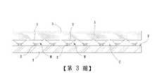
為讓本發明之上述及其他目的、特徵及優點能更明顯易懂,下文特舉本發明之較佳實施例,並配合所附圖式,作詳細說明如下:請參照第3圖所示,本發明的太陽能板抗反射層的製造方法係包含:提供一透明基板1,將至少一導光材料2堆疊於該透明基板1上;將一光學膠3堆疊於該導光材料2上;及將該導光材料2與該透明基板1,以該光學膠3結合於一太陽能板4表面。In order to make the above-mentioned and other objects, features and advantages of the present invention more obvious and easy to understand, the preferred embodiments of the present invention are given below, and the accompanying drawings are described in detail as follows: please refer to Figure 3, The manufacturing method of the solar panel anti-reflection layer of the present invention comprises: providing a
該透明基板1係為高透光率之材質,例如玻璃、藍寶石或壓克力等,在本實施例中,該透明基板1之材質可以為聚甲基丙烯酸甲酯(poly(methyl methacrylate),簡稱PMMA),係具有高透明度、低價格及易於加工等優點。The
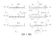
該導光材料2亦為高透光率的材質,該導光材料2可以為選自包含聚二甲基矽氧烷(Polydimethylsiloxane,簡稱PDMS)、聚甲基丙烯酸甲酯、聚碳酸酯(Polycarbonate,簡稱PC)、聚苯乙烯(Polystyrene,簡稱PS)、烯丙基二甘醇碳酸酯(Dially Glycol Carbonates,簡稱CR-39)、SAN樹脂、MS樹脂及聚4-甲基-1戊烯(poly(4-methyl-1-pentene),簡稱PMP)的至少一種。請參照第2圖所示,該導光材料2係以印刷方式逐次印刷於該透明基板1上,使該導光材料2逐層堆疊,進而形成數個微結構M,且各該微結構M為下寬上窄,高度不超過500μm之凸起結構。各該微結構M的各層導光材料2可以置中對齊堆疊,亦可以靠邊對齊堆疊,又,該微結構M的外形可以為例如圓錐形、金字塔形或半球體等,本發明均不予以限制,在本實施例中,係以金字塔形的該微結構M予以說明。The
詳言之,該導光材料2較佳可以透過網版印刷方式印刷於該透明基板1上,藉此,係可以簡單的製程步驟製備該微結構M。請參照第1圖所示,其係以網版印刷該導光材料2(21、22)形成該微結構M之步驟流程。步驟S1:將一網版A1置於該透明基板1的預定印刷位置上,並將未固化的一導光材料21施加於該網版A1上。步驟S2:以一刮板B將該導光材料21抹平於該網版A1,使該導光材料滲入該網版A1的鏤空處,並使該導光材料21結合於該透明基板1上。步驟S3:移除該網版A1,使該導光材料21留置於該透明基板1上,並等待該導光材料21固化。較佳地,在等待該導光材料21固化的過程中,可以對該導光材料21加熱,藉此以減少該導光材料21的固化等待時間。Specifically, the
承上所述,步驟S4:將一網版A2置於已固化的該導光材料21上,並將未固化的一導光材料22施加於該網版A2上,其中,該網版A2的鏤空面積小於該導光材料21的面積。步驟S5:以該刮板B將該導光材料22抹平於該網版A2,使該導光材料22滲入該網版A2的鏤空處,並使該導光材料22結合於該導光材料21上。步驟S6:移除該網版A2,使該導光材料22留置於該導光材料21上,並等待該導光材料22固化,同樣地,對該導光材料22加熱可以加速該導光材料22的固化。重複施作上述步驟S4~S6直到完成預定的堆疊層數,特別說明的是,該網版的鏤空面積係隨著印刷層數的增加而逐漸減少,如此,使該導光材料2的面積逐層縮小,藉此以形成金字塔形的該微結構M。Continuing from the above, step S4: placing a screen plate A2 on the cured
該微結構M各層的該導光材料2可以相同或不同,本發明不予以限制。較佳地,該微結構M可以由不同折射率的數種導光材料2堆疊所形成,且該導光材料2可依折射率由低至高的順序,由該透明基板1往上逐層堆疊。藉此,當光線由大氣進入該微結構M時,折射率變化是以微小的差異漸進,由於各層的該導光材料2之間的折射率變化差異小,因此光線通過該微結構M時造成的反射量可以降低。另外,該微結構M各層的厚度較佳可以為10μm~50μm,藉此可以精確地控制該微結構M的高度。The
請再參照第2圖所示,該光學膠3具有高透光性、高黏著力的特性,該光學膠3係堆疊於該微結構M頂層的該導光材料2上,較佳地,該光學膠3亦可以透過網版印刷的方式印刷於該導光材料2上,藉此,係具有製程簡單的優點。Please refer to FIG. 2 again, the
請參照第3圖所示,當完成該光學膠3的塗覆後,再將該微結構M及該透明基板1倒置,並將將該微結構M及該透明基板1,藉由該光學膠3結合於一太陽能板4的迎光面F,使該微結構M位於該透明基板1及該太陽能板4之間,亦使該透明基板1及該太陽能板4之間形成數個空氣腔室G。藉此,該微結構M係不直接裸露於大氣環境之中,因此,大氣中的粉塵、髒汙不會附著於各該微結構M之間而造成光能損耗及導致太陽能板的發電量降低。Please refer to FIG. 3 , after the coating of the
較佳地,該太陽能板抗反射層另可以包含一抗反射膜5,該抗反射膜5貼覆於該透明基板1的外表面,藉此,係可以減少該透明基板1的光線反射量,進而提高該太陽能板4的光能吸收量。Preferably, the anti-reflection layer of the solar panel may further include an
當該太陽能板4以具備該微結構M陣列及該空氣腔室G的抗反射層吸收光能時,一旦該太陽能板4所反射的光線進入該抗反射層,將因該空氣腔室G與該微結構M之間的折射率差異,而產生部分全反射現象,使得原本被該太陽能板4反射的光線再度回到該太陽能板4中,因此使該太陽能板4增加了光能的利用率,進而提升發電量。而該抗反射層的外表面係為一平滑面,且該微結構M不裸露於大氣環境當中,因此該抗反射層較不容易附著粉塵、髒污而造成光能損耗,該抗反射層亦較易於清潔維護。When the
綜上所述,本發明的太陽能板抗反射層的製造方法,係使用印刷技術形成該微結構,藉此係可以達到節省成本及簡化製程步驟的功效。該微結構係倒置結合於該透明基板,而使該微結構不直接裸露於大氣環境之中,藉此,大氣中的粉塵、髒汙不會附著於各該微結構之間,而造成光能損耗。另外,該微結構可以由不同折射率的數種導光材料,依折射率由低至高的順序堆疊所形成,藉此,係可以降低光線通過該微結構時的反射量的功效。To sum up, the method for manufacturing the anti-reflection layer of the solar panel of the present invention uses the printing technology to form the microstructure, thereby achieving the effects of saving cost and simplifying the process steps. The microstructures are inverted and bonded to the transparent substrate, so that the microstructures are not directly exposed to the atmosphere, so that dust and dirt in the atmosphere will not adhere to the microstructures and cause light energy loss. In addition, the microstructure can be formed by stacking several light-guiding materials with different refractive indices in order from low to high refractive index, thereby reducing the effect of the amount of reflection of light passing through the microstructure.
雖然本發明已利用上述較佳實施例揭示,然其並非用以限定本發明,任何熟習此技藝者在不脫離本發明之精神和範圍之內,相對上述實施例進行各種更動與修改仍屬本發明所保護之技術範疇,因此本發明之保護範圍當視後附之申請專利範圍所界定者為準。Although the present invention has been disclosed by the above-mentioned preferred embodiments, it is not intended to limit the present invention. Any person skilled in the art can make various changes and modifications relative to the above-mentioned embodiments without departing from the spirit and scope of the present invention. Therefore, the scope of protection of the present invention should be determined by the scope of the patent application attached hereto.
1:透明基板1: Transparent substrate
2:導光材料2: Light guide material
3:光學膠3: Optical glue
4:太陽能板4: Solar panels
5:抗反射膜5: Anti-reflection film
F:迎光面F: Greeting surface
G:空氣腔室G: Air chamber
M:微結構M: Microstructure
Claims (9)
Translated fromChinesePriority Applications (1)
| Application Number | Priority Date | Filing Date | Title |
|---|---|---|---|
| TW110112166ATWI771975B (en) | 2021-04-01 | 2021-04-01 | Method for manufacturing anti-reflection layer of a solar panel |
Applications Claiming Priority (1)
| Application Number | Priority Date | Filing Date | Title |
|---|---|---|---|
| TW110112166ATWI771975B (en) | 2021-04-01 | 2021-04-01 | Method for manufacturing anti-reflection layer of a solar panel |
Publications (2)
| Publication Number | Publication Date |
|---|---|
| TWI771975Btrue TWI771975B (en) | 2022-07-21 |
| TW202240922A TW202240922A (en) | 2022-10-16 |
Family
ID=83439655
Family Applications (1)
| Application Number | Title | Priority Date | Filing Date |
|---|---|---|---|
| TW110112166ATWI771975B (en) | 2021-04-01 | 2021-04-01 | Method for manufacturing anti-reflection layer of a solar panel |
Country Status (1)
| Country | Link |
|---|---|
| TW (1) | TWI771975B (en) |
Citations (5)
| Publication number | Priority date | Publication date | Assignee | Title |
|---|---|---|---|---|
| CN101878436A (en)* | 2008-09-29 | 2010-11-03 | 索尼公司 | Optical element, optical part with anti-reflective function, and master |
| CN103069308A (en)* | 2010-08-02 | 2013-04-24 | 光州科学技术院 | Multi-layer silicon non-reflective film with gradually changed refractive index and preparation method thereof, and solar cell with multi-layer silicon non-reflective film and preparation method thereof |
| TW201321299A (en)* | 2011-10-13 | 2013-06-01 | Cambrios Technologies Corp | Photoelectric device combined with metal nanowire |
| CN103606599A (en)* | 2013-11-30 | 2014-02-26 | 浙江光隆能源科技股份有限公司 | Method for manufacturing high-refractive-index silicon nitride antireflection film |
| TWM566911U (en)* | 2018-05-17 | 2018-09-11 | 曾聖嵐 | A solar panel |
- 2021
- 2021-04-01TWTW110112166Apatent/TWI771975B/enactive
Patent Citations (5)
| Publication number | Priority date | Publication date | Assignee | Title |
|---|---|---|---|---|
| CN101878436A (en)* | 2008-09-29 | 2010-11-03 | 索尼公司 | Optical element, optical part with anti-reflective function, and master |
| CN103069308A (en)* | 2010-08-02 | 2013-04-24 | 光州科学技术院 | Multi-layer silicon non-reflective film with gradually changed refractive index and preparation method thereof, and solar cell with multi-layer silicon non-reflective film and preparation method thereof |
| TW201321299A (en)* | 2011-10-13 | 2013-06-01 | Cambrios Technologies Corp | Photoelectric device combined with metal nanowire |
| CN103606599A (en)* | 2013-11-30 | 2014-02-26 | 浙江光隆能源科技股份有限公司 | Method for manufacturing high-refractive-index silicon nitride antireflection film |
| TWM566911U (en)* | 2018-05-17 | 2018-09-11 | 曾聖嵐 | A solar panel |
Also Published As
| Publication number | Publication date |
|---|---|
| TW202240922A (en) | 2022-10-16 |
Similar Documents
| Publication | Publication Date | Title |
|---|---|---|
| CN102986039B (en) | The laminar structure with embedded cavity being used together to solar cell and relevant manufacture method | |
| CN108279459B (en) | Display module and display device | |
| CN102487094B (en) | Solar photoelectric module packaging structure and manufacturing method thereof | |
| CN103336328B (en) | Polarizer component and display device | |
| CN113169237B (en) | Photovoltaic panels | |
| TWI479669B (en) | Solar module high light transmission and light trapping package structure | |
| CN105589251B (en) | Color film substrate, manufacturing method thereof and display device | |
| CN114597279A (en) | Patterned photovoltaic module and preparation method thereof | |
| CN111812773A (en) | A kind of diffractive optical waveguide and preparation method thereof | |
| CN101872795B (en) | Solar module packaging structure | |
| TWI771975B (en) | Method for manufacturing anti-reflection layer of a solar panel | |
| CN105676321B (en) | A kind of preparation method of lenticule nano-pore mixing array structure | |
| CN209433049U (en) | Light guide decorative plate and lamp decoration module | |
| CN102315293B (en) | Solar photovoltaic module encapsulation laminated structure and manufacturing method thereof | |
| CN114270539A (en) | Photovoltaic module | |
| CN102565914B (en) | Light conductor and manufacture method thereof | |
| AU2020213717B2 (en) | Optical structure for solar applications and manufacturing method | |
| CN103257478A (en) | Composite type optical film and manufacturing method thereof | |
| CN222913908U (en) | Front light plate structure of reflective display | |
| CN217932148U (en) | Optical article | |
| CN210123511U (en) | Optical diaphragm group and backlight module | |
| CN120529655A (en) | Functional film and preparation method and application thereof | |
| CN119682269A (en) | Preparation method of light control film and its product | |
| TW201517294A (en) | Method for manufacturing nanostructure of solar cell | |
| CN107445477B (en) | Method for manufacturing energy-saving glass |