TWI769119B - Electronic package and manufacturing method thereof - Google Patents
Electronic package and manufacturing method thereofDownload PDFInfo
- Publication number
- TWI769119B TWI769119BTW110149402ATW110149402ATWI769119BTW I769119 BTWI769119 BTW I769119BTW 110149402 ATW110149402 ATW 110149402ATW 110149402 ATW110149402 ATW 110149402ATW I769119 BTWI769119 BTW I769119B
- Authority
- TW
- Taiwan
- Prior art keywords
- antenna
- layer
- electronic package
- package
- insulating spacer
- Prior art date
Links
- 238000004519manufacturing processMethods0.000titleclaimsdescription27
- 239000010410layerSubstances0.000claimsdescription148
- 125000006850spacer groupChemical group0.000claimsdescription40
- 238000005253claddingMethods0.000claimsdescription26
- 238000000034methodMethods0.000claimsdescription11
- 239000011247coating layerSubstances0.000claimsdescription5
- 230000005611electricityEffects0.000claims1
- 239000004642PolyimideSubstances0.000description11
- 229920001721polyimidePolymers0.000description11
- 238000004891communicationMethods0.000description10
- 239000000463materialSubstances0.000description10
- 239000000758substrateSubstances0.000description10
- 239000004020conductorSubstances0.000description9
- 239000012790adhesive layerSubstances0.000description7
- 230000001681protective effectEffects0.000description6
- RYGMFSIKBFXOCR-UHFFFAOYSA-NCopperChemical compound[Cu]RYGMFSIKBFXOCR-UHFFFAOYSA-N0.000description4
- 229910052802copperInorganic materials0.000description4
- 239000010949copperSubstances0.000description4
- 239000003989dielectric materialSubstances0.000description4
- 230000008569processEffects0.000description4
- 229910000679solderInorganic materials0.000description4
- 230000000694effectsEffects0.000description3
- 238000005516engineering processMethods0.000description3
- 238000000465mouldingMethods0.000description3
- 239000005022packaging materialSubstances0.000description3
- 239000004065semiconductorSubstances0.000description3
- 230000005540biological transmissionEffects0.000description2
- 150000001875compoundsChemical class0.000description2
- 239000012792core layerSubstances0.000description2
- 238000010586diagramMethods0.000description2
- 238000007772electroless platingMethods0.000description2
- 239000011810insulating materialSubstances0.000description2
- 238000009413insulationMethods0.000description2
- 239000002184metalSubstances0.000description2
- 229910052751metalInorganic materials0.000description2
- 239000007769metal materialSubstances0.000description2
- 230000004048modificationEffects0.000description2
- 238000012986modificationMethods0.000description2
- 238000004806packaging method and processMethods0.000description2
- 239000004593EpoxySubstances0.000description1
- YCKRFDGAMUMZLT-UHFFFAOYSA-NFluorine atomChemical group[F]YCKRFDGAMUMZLT-UHFFFAOYSA-N0.000description1
- 230000009471actionEffects0.000description1
- 239000003990capacitorSubstances0.000description1
- 230000001413cellular effectEffects0.000description1
- 230000008859changeEffects0.000description1
- 239000011248coating agentSubstances0.000description1
- 238000000576coating methodMethods0.000description1
- 239000013078crystalSubstances0.000description1
- 230000007812deficiencyEffects0.000description1
- 230000005672electromagnetic fieldEffects0.000description1
- 238000009713electroplatingMethods0.000description1
- 239000003822epoxy resinSubstances0.000description1
- 238000005530etchingMethods0.000description1
- 229910052731fluorineInorganic materials0.000description1
- 239000011737fluorineSubstances0.000description1
- 239000011521glassSubstances0.000description1
- PCHJSUWPFVWCPO-UHFFFAOYSA-NgoldChemical compound[Au]PCHJSUWPFVWCPO-UHFFFAOYSA-N0.000description1
- 229910052737goldInorganic materials0.000description1
- 239000010931goldSubstances0.000description1
- 238000000227grindingMethods0.000description1
- 230000010354integrationEffects0.000description1
- 230000002452interceptive effectEffects0.000description1
- 238000003475laminationMethods0.000description1
- 239000012528membraneSubstances0.000description1
- 238000005272metallurgyMethods0.000description1
- 238000010295mobile communicationMethods0.000description1
- 229920002577polybenzoxazolePolymers0.000description1
- 229920000647polyepoxidePolymers0.000description1
- 230000005855radiationEffects0.000description1
- 229910052710siliconInorganic materials0.000description1
- 239000010703siliconSubstances0.000description1
- 239000007787solidSubstances0.000description1
- 238000004544sputter depositionMethods0.000description1
- 238000007740vapor depositionMethods0.000description1
Images


Classifications
- H—ELECTRICITY
- H01—ELECTRIC ELEMENTS
- H01Q—ANTENNAS, i.e. RADIO AERIALS
- H01Q1/00—Details of, or arrangements associated with, antennas
- H01Q1/36—Structural form of radiating elements, e.g. cone, spiral, umbrella; Particular materials used therewith
- H01Q1/38—Structural form of radiating elements, e.g. cone, spiral, umbrella; Particular materials used therewith formed by a conductive layer on an insulating support
- H—ELECTRICITY
- H01—ELECTRIC ELEMENTS
- H01L—SEMICONDUCTOR DEVICES NOT COVERED BY CLASS H10
- H01L23/00—Details of semiconductor or other solid state devices
- H01L23/58—Structural electrical arrangements for semiconductor devices not otherwise provided for, e.g. in combination with batteries
- H01L23/64—Impedance arrangements
- H01L23/66—High-frequency adaptations
- H—ELECTRICITY
- H01—ELECTRIC ELEMENTS
- H01Q—ANTENNAS, i.e. RADIO AERIALS
- H01Q1/00—Details of, or arrangements associated with, antennas
- H01Q1/50—Structural association of antennas with earthing switches, lead-in devices or lightning protectors
- H—ELECTRICITY
- H01—ELECTRIC ELEMENTS
- H01L—SEMICONDUCTOR DEVICES NOT COVERED BY CLASS H10
- H01L2223/00—Details relating to semiconductor or other solid state devices covered by the group H01L23/00
- H01L2223/58—Structural electrical arrangements for semiconductor devices not otherwise provided for
- H01L2223/64—Impedance arrangements
- H01L2223/66—High-frequency adaptations
- H01L2223/6661—High-frequency adaptations for passive devices
- H01L2223/6677—High-frequency adaptations for passive devices for antenna, e.g. antenna included within housing of semiconductor device
Landscapes
- Physics & Mathematics (AREA)
- Condensed Matter Physics & Semiconductors (AREA)
- General Physics & Mathematics (AREA)
- Engineering & Computer Science (AREA)
- Computer Hardware Design (AREA)
- Microelectronics & Electronic Packaging (AREA)
- Power Engineering (AREA)
- Support Of Aerials (AREA)
- Details Of Aerials (AREA)
- Encapsulation Of And Coatings For Semiconductor Or Solid State Devices (AREA)
Abstract
Description
Translated fromChinese本發明係有關一種電子封裝件,尤指一種具天線結構之電子封裝件及其製法。The present invention relates to an electronic package, in particular to an electronic package with an antenna structure and a manufacturing method thereof.
目前無線通訊技術已廣泛應用於各式消費性電子產品(如手機、平板電腦等),以利接收或發送各種無線訊號。此外,為滿足消費性電子產品的攜帶及上網便利性,無線通訊模組之製造與設計係朝輕、薄、短、小之需求作開發,其中,平面天線(Patch Antenna)因具有體積小、重量輕與製造容易等特性而廣泛利用在電子產品之無線通訊模組中。At present, wireless communication technology has been widely used in various consumer electronic products (such as mobile phones, tablet computers, etc.) to facilitate receiving or sending various wireless signals. In addition, in order to meet the convenience of carrying and surfing the Internet of consumer electronic products, the manufacture and design of wireless communication modules are developed towards the needs of light, thin, short and small. It is widely used in wireless communication modules of electronic products due to its characteristics of light weight and easy manufacture.
目前5G之相關應用技術於未來將全面商品化,其應用頻率範圍約在1GHz~1000GHz之間的高頻頻段,其商業應用模式為5G搭配4G LTE,並於戶外架設一蜂巢式基站以配合設於室內的小基站,故5G行動通訊會於基站內使用大量天線以符合5G系統的大容量快速傳輸且低延遲之要求。At present, the related application technology of 5G will be fully commercialized in the future. Its application frequency range is about 1GHz~1000GHz high frequency band. Its commercial application mode is 5G with 4G LTE, and a cellular base station is set up outdoors to match For indoor small base stations, 5G mobile communication will use a large number of antennas in the base station to meet the requirements of the 5G system for large-capacity, fast transmission and low latency.
圖1係習知無線通訊模組之立體示意圖。如圖1所示,該無線通訊模組1係包括:一基板10、設於該基板10上之複數電子元件11、一天線結構12以及封裝材13。該基板10係為電路板並呈矩形體。該電子元件11係設於該基板10上且電性連接該基板10。該天線結構12係為平面型且具有一天線本體120與一導線121,該天線本體120藉由該導線121電性連接該電子元件11。該封裝材13覆蓋該電子元件11與該部分導線121。FIG. 1 is a three-dimensional schematic diagram of a conventional wireless communication module. As shown in FIG. 1 , the
惟,習知無線通訊模組1中,其僅能配置單一天線結構12,因而限制該無線通訊模組1之天線功能,造成該無線通訊模組1無法提供運作5G系統所需之電性功能,難以達到5G系統之天線運作之需求。However, in the conventional
因此,如何克服上述習知技術的問題,實已成目前亟欲解決的課題。Therefore, how to overcome the above-mentioned problems of the conventional technology has become an urgent problem to be solved at present.
鑑於上述習知技術之種種缺失,本發明係提供一種電子封裝件,係包括:封裝模組,係於內部配置有複數饋入線路,其中,該複數饋入線路係定義有第一天線層及第二天線層;絕緣間隔體,係設於該封裝模組之部分表面上;第一天線體,係對應該第一天線層之位置設於該絕緣間隔體上,且使該第一天線體與該第一天線層位於該絕緣間隔體之相對兩側,以令該第一天線體與該第一天線層形成第一天線結構;以及第二天線體,係對應該第二天線層之位置設於封裝模組之部分表面上,且使該第二天線體與該第二天線層之間保持距離,以令該第二天線體與該第二天線層形成第二天線結構。In view of various deficiencies in the above-mentioned prior art, the present invention provides an electronic package, which includes: a package module, which is internally configured with a plurality of feed lines, wherein the plurality of feed lines are defined with a first antenna layer and a second antenna layer; an insulating spacer is arranged on a part of the surface of the package module; a first antenna body is arranged on the insulating spacer corresponding to the position of the first antenna layer, and makes the a first antenna body and the first antenna layer are located on opposite sides of the insulating spacer, so that the first antenna body and the first antenna layer form a first antenna structure; and a second antenna body , which is located on a part of the surface of the package module corresponding to the position of the second antenna layer, and keeps a distance between the second antenna body and the second antenna layer, so that the second antenna body and the The second antenna layer forms a second antenna structure.
本發明亦提供一種電子封裝件之製法,係包括:提供一封裝模組,其內部係配置有複數饋入線路,其中,該複數饋入線路係定義有第一天線層及第二天線層;將絕緣間隔體設於該封裝模組之部分表面上;對應該第一天線層之位置而於該絕緣間隔體上形成第一天線體,且使該第一天線體與該第一天線層位於該絕緣間隔體之相對兩側,以令該第一天線體與該第一天線層形成第一天線結構;以及對應該第二天線層之位置而於封裝模組之部分表面上形成第二天線體,且使該第二天線體與該第二天線層之間保持距離,以令該第二天線體與該第二天線層形成第二天線結構。The present invention also provides a method of manufacturing an electronic package, which includes: providing a package module, the interior of which is configured with a plurality of feed lines, wherein the plurality of feed lines are defined with a first antenna layer and a second antenna layer; an insulating spacer is arranged on a part of the surface of the package module; a first antenna body is formed on the insulating spacer corresponding to the position of the first antenna layer, and the first antenna body and the first antenna levelon opposite sides of the insulating spacer, so that the first antenna body and the first antenna layer form a first antenna structure; and corresponding to the position of the second antenna layer on a part of the surface of the package module A second antenna body is formed thereon, and a distance is maintained between the second antenna body and the second antenna layer, so that the second antenna body and the second antenna layer form a second antenna structure.
前述之電子封裝件及其製法中,該第一天線結構之適用頻率為24~52吉赫。In the aforementioned electronic package and its manufacturing method, the applicable frequency of the first antenna structure is 24-52 GHz.
前述之電子封裝件及其製法中,該第一天線體與該第一天線層係以耦合方式傳輸訊號。In the aforementioned electronic package and the manufacturing method thereof, the first antenna body and the first antenna layer transmit signals in a coupled manner.
前述之電子封裝件及其製法中,該絕緣間隔體係為介電層。In the aforementioned electronic package and its manufacturing method, the insulating spacer system is a dielectric layer.
前述之電子封裝件及其製法中,該絕緣間隔體之介電係數係小於3。In the aforementioned electronic package and its manufacturing method, the dielectric coefficient of the insulating spacer is less than 3.
前述之電子封裝件及其製法中,該第二天線結構之適用頻率為410~7125兆赫。In the aforementioned electronic package and its manufacturing method, the applicable frequency of the second antenna structure is 410-7125 MHz.
前述之電子封裝件及其製法中,該第二天線體與該第二天線層係以耦合方式傳輸訊號。In the aforementioned electronic package and its manufacturing method, the second antenna body and the second antenna layer transmit signals in a coupled manner.
前述之電子封裝件及其製法中,該封裝模組係包含有至少一電子元件及一包覆該電子元件之包覆層,以令該第二天線體與該第二天線層位於該包覆層之相對兩側。例如,該包覆層之介電係數係小於3.7。或者,該封裝模組復包含有埋設於該包覆層中之複數導電柱,以及配置於該包覆層相對兩側以藉由該複數導電柱相互電性連接之承載結構與線路結構,以令該承載結構佈設有該第一天線層,且該線路結構佈設有該第二天線層,並使該絕緣間隔體與該第二天線體設於該承載結構之一表面上。In the aforementioned electronic package and its manufacturing method, the package module includes at least one electronic component and a coating layer covering the electronic component, so that the second antenna body and the second antenna layer are located in the opposite sides of the cladding. For example, the dielectric constant of the cladding layer is less than 3.7. Or, the package module further includes a plurality of conductive pillars embedded in the cladding layer, and a bearing structure and a circuit structure disposed on opposite sides of the cladding layer to be electrically connected to each other through the plurality of conductive pillars, so as to The carrier structure is arranged with the first antenna layer, the circuit structure is arranged with the second antenna layer, and the insulating spacer and the second antenna body are arranged on a surface of the carrier structure.
由上可知,本發明之電子封裝件及其製法中,主要藉由利用絕緣間隔體將該第一天線結構與第二天線結構整合該封裝模組上,且該第一天線結構之射頻與該第二天線結構之射頻不同,使該電子元件可依需求發出/接收不同之天線訊號,以令應用該電子封裝件之電子產品傳接所需頻率之訊號,故相較於習知技術,該電子封裝件係配置多組天線結構,因而可提升該電子產品之天線功能,使該電子產品可提供運作5G系統所需之電性功能,以達到5G系統之天線運作之需求。As can be seen from the above, in the electronic package of the present invention and the manufacturing method thereof, the first antenna structure and the second antenna structure are mainly integrated on the package module by using an insulating spacer, and the first antenna structure is formed.The radio frequency of the structure is different from the radio frequency of the second antenna structure, so that the electronic component can send/receive different antenna signals according to the requirements, so that the electronic product using the electronic package can transmit the signal of the required frequency. In the prior art, the electronic package is configured with multiple sets of antenna structures, so that the antenna function of the electronic product can be improved, so that the electronic product can provide the electrical functions required for the operation of the 5G system, so as to achieve the antenna operation of the 5G system. need.
1:無線通訊模組1: Wireless communication module
10:基板10: Substrate
11,21:電子元件11,21: Electronic Components
12:天線結構12: Antenna structure
120:天線本體120: Antenna body
121:導線121: Wire
13:封裝材13: Packaging material
2:電子封裝件2: Electronic packages
2a:封裝模組2a: Package module
20:承載結構20: Bearing structure
20a:第一側20a: First side
20b:第二側20b: Second side
200:第一絕緣層200: first insulating layer
201:第一線路層201: The first circuit layer
21a:作用面21a: Action surface
21b:非作用面21b: Non-active surface
210:電極墊210: Electrode pads
211:保護膜211: Protective film
212:固晶層212: solid crystal layer
22:導電體22: Conductor
23:導電柱23: Conductive column
24:絕緣間隔體24: Insulation spacer
25:包覆層25: Cladding
26:線路結構26: Line structure
260:第二絕緣層260: Second insulating layer
261:第二線路層261: Second circuit layer
27:導電元件27: Conductive elements
270:凸塊底下金屬層270: Metal layer under bump
28:第一天線結構28: The first antenna structure
28a:第一天線層28a: first antenna layer
28b:第一天線體28b: first antenna body
29:第二天線結構29: Second Antenna Structure
29a:第二天線層29a: Second Antenna Layer
29b:第二天線體29b: Second antenna body
9:支撐板9: Support plate
90:離型層90: release layer
91:黏著層91: Adhesive layer
圖1係為習知無線通訊模組之立體示意圖。FIG. 1 is a three-dimensional schematic diagram of a conventional wireless communication module.
圖2A至圖2E係為本發明之電子封裝件之製法的剖面示意圖。2A to 2E are schematic cross-sectional views of a method for manufacturing an electronic package of the present invention.
圖2F係為圖2E之上視平面示意圖。FIG. 2F is a schematic top plan view of FIG. 2E .
以下藉由特定的具體實施例說明本發明之實施方式,熟悉此技藝之人士可由本說明書所揭示之內容輕易地瞭解本發明之其他優點及功效。The following specific embodiments are used to illustrate the implementation of the present invention, and those skilled in the art can easily understand other advantages and effects of the present invention from the contents disclosed in this specification.
須知,本說明書所附圖式所繪示之結構、比例、大小等,均僅用以配合說明書所揭示之內容,以供熟悉此技藝之人士之瞭解與閱讀,並非用以限定本發明可實施之限定條件,故不具技術上之實質意義,任何結構之修飾、比例關係之改變或大小之調整,在不影響本發明所能產生之功效及所能達成之目的下,均應仍落在本發明所揭示之技術內容得能涵蓋之範圍內。同時,本說明書中所引用之如「上」、「第一」、「第二」及「一」等之用語,亦僅為便於敘述之明瞭,而非用以限定本發明可實施之範圍,其相對關係之改變或調整,在無實質變更技術內容下,當亦視為本發明可實施之範疇。It should be noted that the structures, proportions, sizes, etc. shown in the drawings in this specification are only used to cooperate with the contents disclosed in the specification for the understanding and reading of those who are familiar with the art, and are not intended to limit the implementation of the present invention. Therefore, it has no technical significance. Any modification of the structure, change of the proportional relationship or adjustment of the size should still fall within the scope of the present invention without affecting the effect and the purpose that the present invention can achieve. The technical content disclosed by the invention can be covered within the scope. At the same time, the terms such as "above", "first", "second" and "one" quoted in this specification are only for the convenience of description, and are not used to limit the scope of the present invention. Changes or adjustments to their relative relationships, without substantial changes to the technical content, should also be regarded as the scope of the present invention.
圖2A至圖2E係為本發明之電子封裝件2之製法的剖面示意圖。2A to 2E are schematic cross-sectional views of a method of manufacturing the
如圖2A所示,於一支撐板9上結合有承載結構20,該承載結構20具有相對之第一側20a與第二側20b,且該承載結構20以其第二側20b結合至該支撐板9上。接著,於該承載結構20之第一側20a上形成複數電性連接該承載結構20之導電柱23,且設置至少一電子元件21於該承載結構20之第一側20a上。As shown in FIG. 2A , a supporting
所述之承載結構20係為線路構造或基板構造,該基板構造係為具有核心層型式或無核心層型式,例如,具有核心層與線路結構之封裝基板(substrate)或無核心層(coreless)之線路基板構造,其中,該承載結構20包括至少一第一絕緣層200與設於該第一絕緣層200上之第一線路層201,如線路重佈層(redistribution layer,簡稱RDL)。The
於本實施例中,形成該第一線路層201之材質係為銅,且形成該第一絕緣層200之材質係為如聚對二唑苯(Polybenzoxazole,簡稱PBO)、聚醯亞胺(Polyimide,簡稱PI)、預浸材(Prepreg,簡稱PP)等之介電材。In this embodiment, the material for forming the
再者,該承載結構20復配置有電性連接該第一線路層201之第一天線層28a。例如,該第一天線層28a係與該第一線路層201一起藉由RDL製程製作。Furthermore, the
所述之支撐板9係例如為半導體材(如矽或玻璃)板體,其上以塗佈方式依序形成有一離型層90與一黏著層91,以供該承載結構20設於該黏著層91上。The
所述之導電柱23係例如為柱狀體、線狀體或球狀體,其立設於該第一線路層201上並電性連接該第一線路層201。The
於本實施例中,形成該導電柱23之材質係為如銅、金之金屬材或銲錫材,但並不限於上述。In this embodiment, the material for forming the
所述之電子元件21係為主動元件、被動元件或其二者組合,且該主動元件係例如半導體晶片,而該被動元件係例如電阻、電容及電感。The
於本實施例中,該電子元件21係為半導體晶片,其具有相對之作用面21a與非作用面21b,該電子元件21係以其非作用面21b藉由一固晶層212黏固於該承載結構20之第一側20a上,且該作用面21a具有複數電極墊210,並於該複數電極墊210上形成有複數導電體22與覆蓋該複數電極墊210與該複數導電體22之保護膜211。例如,該保護膜211係例如為聚對二唑苯(PBO)之絕緣材,且該導電體22係為如導電線路、銲球之圓球狀、或如銅柱、銲錫凸塊等金屬材之柱狀、或銲線機製作之釘狀(stud),但不限於此。In this embodiment, the
如圖2B所示,形成一包覆層25於該承載結構20之第一側20a上,以令該包覆層25包覆該電子元件21與該複數導電柱23,再藉由整平製程,令該包覆層25之上表面與保護膜211之上表面、該複數導電柱23之端面及該複數導電體22之端面共平面,使該保護膜211之上表面、該導電柱23之端面與該導電體22之端面外露於該包覆層25。As shown in FIG. 2B, a
於本實施例中,該包覆層25係為絕緣材,如聚醯亞胺(polyimide,簡稱PI)、乾膜(dry film)、環氧樹脂(epoxy)或封裝材(molding compound),其可用壓合(lamination)或模壓(molding)之方式形成於該承載結構20之第一側20a上。In this embodiment, the
再者,該整平製程係藉由研磨方式,移除該導電柱23、保護膜211、導電體22與包覆層25之部分材質,而使該包覆層25之上表面與保護膜211之上表面、該導電柱23之端面及該導電體22之端面共平面。Furthermore, the leveling process removes part of the material of the
如第2C圖所示,形成一線路結構26於該包覆層25上,使該線路結構26堆疊於該承載結構20上以形成一封裝模組2a。As shown in FIG. 2C, a
於本實施例中,該線路結構26係包含有複數第二絕緣層260、及設於該第二絕緣層260上之複數如RDL之第二線路層261,以令該第二線路層261電性連接該複數導電柱23與該電子元件21上之複數導電體22。或者,該線路結構26亦可僅包括單一第二絕緣層260及單一第二線路層261。In this embodiment, the
再者,形成該第二線路層261之材質係為銅,且形成該第二絕緣層260之材質係為如聚對二唑苯(PBO)、聚醯亞胺(PI)、預浸材(PP)之介電材。Furthermore, the material for forming the
又,該線路結構26復配置有電性連接該第二線路層261之第二天線層29a。例如,該第二天線層29a係與該第二線路層261一起藉由RDL製程製作。In addition, the
另外,形成複數如銲球之導電元件27於最外層之第二線路層261上。例如,可形成一凸塊底下金屬層(Under Bump Metallurgy,簡稱UBM)270於最外層之第二線路層261上,以利於結合該導電元件27。應可理解地,有關封裝模組2a之種類繁多,並不限於上述,特此述明。In addition, a plurality of
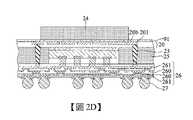
如圖2D所示,移除該支撐板9及該離型層90,再進行翻轉,以於該承載結構20之第二側20b之黏著層91之部分表面上形成一絕緣間隔體24。As shown in FIG. 2D , the
於本實施例中,該絕緣間隔體24係為介電層,如聚醯亞胺(polyimide,簡稱PI)、乾膜(dry film)或封裝材(molding compound)等介電材,但並不限於上述。例如,先將一介電層塗佈於該黏著層91之全部表面上,再以蝕刻方式移除該介電層之部分材質,以形成該絕緣間隔體24。In this embodiment, the insulating
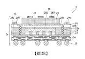
如圖2E所示,於該絕緣間隔體24上形成一對應該第一天線層28a配置之第一天線體28b,以令該第一天線體28b與第一天線層28a位於該絕緣間隔體24之相對兩側而形成第一天線結構28,且於該承載結構20之第二側20b之黏著層91之部分表面上形成一對應該第二天線層29a配置之第二天線體29b,以令該第二天線體29b與第二天線層29a之間保持距離而形成第二天線結構29,並使該第二天線體29b環繞該第一天線體28b,如圖2F所示。As shown in FIG. 2E, a pair of
於本實施例中,以6吉赫(GHz)頻段為界線,該第一天線結構28係為高頻段天線,即高於6GHz,且該第二天線結構29係為低頻段天線,即6GHz以下(俗稱Sub-6GHz)。例如,該電子元件21藉由該第一天線結構28收發24~53吉赫(GHz)頻率之高頻5G毫米波(mmWave)訊號,且該電子元件21藉由該第二天線結構29收發Sub-6GHz(約410~7125兆赫(MHz))頻率之低頻5G毫米波訊號。In this embodiment, taking the 6 gigahertz (GHz) frequency band as the boundary, the
再者,該第一天線體28b與第一天線層28a係以耦合方式傳輸訊號,並使該第一天線層28a作為該第一天線結構28之饋入線路,且該第二天線體29b與第二天線層29a亦以耦合方式傳輸訊號,並使該第二天線層29a作為該第二天線結構29之饋入線路。例如,該天線層與該天線體係可由交變電壓、交變電流或輻射變化產生輻射能量,且該輻射能量係為電磁場,以令該天線層與該天線體能相互電磁耦合,使天線訊號能於該天線層與該天線體之間傳遞。另外,第二天線層29a與第二天線體29b之間無其他金屬層。Furthermore, the
又,配合該高頻段天線之介質區域(如該絕緣間隔體24與第一絕緣層200),其介電係數需小於3,例如,SiLK、MSQ、PI(含奈米空氣、氟基團)或其它適當材質;另一方面,配合該低頻段天線之介質區域(如第一絕緣層200、包覆層25與第二絕緣層260),其介電係數需小於3.7,例如,環氧樹脂、PI或其它適當材質。In addition, the dielectric region of the high-frequency antenna (such as the insulating
另外,可藉由濺鍍(sputtering)、蒸鍍(vaporing)、電鍍、無電電鍍、化鍍或貼膜(foiling)等方式製作第一天線體28b與第二天線體29b。In addition, the
因此,本發明之製法主要藉由該絕緣間隔體24之配置,以利於將該第一天線結構28與第二天線結構29整合於該封裝模組2a上而不相互干涉,使該電子封裝件2可依需求發出/接收不同之天線訊號,故相較於習知技術,該電子封裝件2可配置包含多種頻率之天線結構,使單一該電子封裝件2即可對應多種頻率之射頻產品之需求,因而能提升該電子產品之天線功能,致能提供運作5G系統所需之電性功能,以達到5G系統之天線運作之需求。Therefore, the manufacturing method of the present invention mainly relies on the configuration of the insulating
本發明復提供一種電子封裝件2,其包括:一封裝模組2a、絕緣間隔體24、第一天線體28b以及第二天線體29b。The present invention further provides an
所述之封裝模組2a係於內部配置有複數饋入線路,其中,該複數饋入線路係定義有第一天線層28a及第二天線層29a。The
所述之絕緣間隔體24係設於該封裝模組2a之部分表面上。The insulating
所述之第一天線體28b係對應該第一天線層28a之位置而設於該絕緣間隔體24上,且該第一天線體28b與該第一天線層28a係位於該絕緣間隔體24之相對兩側,以令該第一天線體28b與該第一天線層28a形成第一天線結構28。The
所述之第二天線體29b係對應該第二天線層29a之位置而設於該封裝模組2a之部分表面上,且該第二天線體29b與該第二天線層29a之間係保持距離而相互分隔,以令該第二天線體29b與該第二天線層29a形成第二天線結構29。The
於一實施例中,該第一天線結構28之適用頻率為24~52吉赫。In one embodiment, the applicable frequency of the
於一實施例中,該第一天線體28b與該第一天線層28a係以耦合方式傳輸訊號。In one embodiment, the
於一實施例中,該絕緣間隔體24係為介電層。In one embodiment, the insulating
於一實施例中,該絕緣間隔體24之介電係數係小於3。In one embodiment, the dielectric coefficient of the insulating
於一實施例中,該第二天線結構29之適用頻率為410~7125兆赫。In one embodiment, the applicable frequency of the
於一實施例中,該第二天線體29b與該第二天線層29a係以耦合方式傳輸訊號。In one embodiment, the
於一實施例中,該封裝模組2a係包含有至少一電子元件21及一包覆該電子元件21之包覆層25,以令該第二天線體29b與該第二天線層29a位於該包覆層25之相對兩側。例如,該包覆層25之介電係數係小於3.7。進一步,該封裝模組2a復包含有埋設於該包覆層25中之複數導電柱23、及配置於該包覆層25相對兩側以藉由該複數導電柱23相互電性連接之承載結構20與線路結構26,以令該承載結構20佈設有該第一天線層28a,且該線路結構26佈設有該第二天線層29a,並使該絕緣間隔體24與該第二天線體29b均設於該承載結構20之一表面上。In one embodiment, the
綜上所述,本發明之電子封裝件及其製法係藉由該絕緣間隔體之設計,以將該第一天線結構與第二天線結構整合該封裝模組,且該第一天線結構之射頻與該第二天線結構之射頻不同,使電子封裝件包含兩種頻段(Sub-6G或mmWave)的訊號接收能力,故應用該電子封裝件之電子產品能對應多種頻率之射頻產品之需求。To sum up, the electronic package of the present invention and its manufacturing method are based on the design of the insulating spacer to integrate the first antenna structure and the second antenna structure into the package module, and the first antenna The radio frequency of the structure is different from the radio frequency of the second antenna structure, so that the electronic package contains the signal receiving capability of two frequency bands (Sub-6G or mmWave), so the electronic products using the electronic package can correspond to the radio frequency products of various frequencies demand.
上述實施例係用以例示性說明本發明之原理及其功效,而非用於限制本發明。任何熟習此項技藝之人士均可在不違背本發明之精神及範疇下,對上述實施例進行修改。因此本發明之權利保護範圍,應如後述之申請專利範圍所列。The above embodiments are used to illustrate the principles and effects of the present invention, but not to limit the present invention. Any person skilled in the art can make modifications to the above embodiments without departing from the spirit and scope of the present invention. Therefore, the scope of protection of the right of the present invention should be listed in the scope of the patent application described later.
2:電子封裝件2: Electronic packages
2a:封裝模組2a: Package module
20:承載結構20: Bearing structure
20a:第一側20a: First side
20b:第二側20b: Second side
21:電子元件21: Electronic Components
23:導電柱23: Conductive column
24:絕緣間隔體24: Insulation spacer
25:包覆層25: Cladding
26:線路結構26: Line structure
27:導電元件27: Conductive elements
28:第一天線結構28: First Antenna Structure
28a:第一天線層28a: first antenna layer
28b:第一天線體28b: first antenna body
29:第二天線結構29: Second Antenna Structure
29a:第二天線層29a: Second Antenna Layer
29b:第二天線體29b: Second antenna body
91:黏著層91: Adhesive layer
Claims (20)
Translated fromChinesePriority Applications (2)
| Application Number | Priority Date | Filing Date | Title |
|---|---|---|---|
| TW110149402ATWI769119B (en) | 2021-12-29 | 2021-12-29 | Electronic package and manufacturing method thereof |
| CN202210020592.8ACN116417785A (en) | 2021-12-29 | 2022-01-10 | Electronic package and method for manufacturing the same |
Applications Claiming Priority (1)
| Application Number | Priority Date | Filing Date | Title |
|---|---|---|---|
| TW110149402ATWI769119B (en) | 2021-12-29 | 2021-12-29 | Electronic package and manufacturing method thereof |
Publications (2)
| Publication Number | Publication Date |
|---|---|
| TWI769119Btrue TWI769119B (en) | 2022-06-21 |
| TW202326872A TW202326872A (en) | 2023-07-01 |
Family
ID=83104126
Family Applications (1)
| Application Number | Title | Priority Date | Filing Date |
|---|---|---|---|
| TW110149402ATWI769119B (en) | 2021-12-29 | 2021-12-29 | Electronic package and manufacturing method thereof |
Country Status (2)
| Country | Link |
|---|---|
| CN (1) | CN116417785A (en) |
| TW (1) | TWI769119B (en) |
Families Citing this family (2)
| Publication number | Priority date | Publication date | Assignee | Title |
|---|---|---|---|---|
| CN119627026A (en)* | 2023-09-14 | 2025-03-14 | 青岛新核芯科技有限公司 | Electronic packaging and method of manufacturing the same |
| TWI860156B (en)* | 2023-11-07 | 2024-10-21 | 矽品精密工業股份有限公司 | Electronic package and method for fabricating thereof |
Citations (5)
| Publication number | Priority date | Publication date | Assignee | Title |
|---|---|---|---|---|
| US20100327068A1 (en)* | 2009-06-30 | 2010-12-30 | International Business Machines Corporation | Compact millimeter wave packages with integrated antennas |
| US20140333505A1 (en)* | 2001-05-17 | 2014-11-13 | Cypress Semiconductor Corporation | Semiconductor package having integrated antenna pad |
| CN109755227A (en)* | 2019-01-09 | 2019-05-14 | 中芯长电半导体(江阴)有限公司 | Encapsulating structure and preparation method thereof |
| US20200168592A1 (en)* | 2017-12-13 | 2020-05-28 | Intel Corporation | Systems in packages including wide-band phased-array antennas and methods of assembling same |
| TW202115796A (en)* | 2019-09-30 | 2021-04-16 | 台灣積體電路製造股份有限公司 | Antenna package, system of antenna package and method of manufacturing antenna package |
Family Cites Families (7)
| Publication number | Priority date | Publication date | Assignee | Title |
|---|---|---|---|---|
| JP4658914B2 (en)* | 2006-12-06 | 2011-03-23 | Okiセミコンダクタ株式会社 | Semiconductor device and manufacturing method thereof |
| US9413079B2 (en)* | 2013-03-13 | 2016-08-09 | Intel Corporation | Single-package phased array module with interleaved sub-arrays |
| US10510693B2 (en)* | 2017-09-28 | 2019-12-17 | Taiwan Semiconductor Manufacturing Co., Ltd. | Semiconductor package structure |
| TWI640066B (en)* | 2017-11-03 | 2018-11-01 | 矽品精密工業股份有限公司 | An electronic package and method of fabricating thereof |
| CN108305856B (en)* | 2018-03-16 | 2023-08-18 | 盛合晶微半导体(江阴)有限公司 | Antenna packaging structure and packaging method |
| TWI700801B (en)* | 2019-09-16 | 2020-08-01 | 矽品精密工業股份有限公司 | Electronic package and method for manufacturing the same |
| US12293980B2 (en)* | 2019-09-20 | 2025-05-06 | Qualcomm Incorporated | Package comprising discrete antenna device |
- 2021
- 2021-12-29TWTW110149402Apatent/TWI769119B/enactive
- 2022
- 2022-01-10CNCN202210020592.8Apatent/CN116417785A/enactivePending
Patent Citations (5)
| Publication number | Priority date | Publication date | Assignee | Title |
|---|---|---|---|---|
| US20140333505A1 (en)* | 2001-05-17 | 2014-11-13 | Cypress Semiconductor Corporation | Semiconductor package having integrated antenna pad |
| US20100327068A1 (en)* | 2009-06-30 | 2010-12-30 | International Business Machines Corporation | Compact millimeter wave packages with integrated antennas |
| US20200168592A1 (en)* | 2017-12-13 | 2020-05-28 | Intel Corporation | Systems in packages including wide-band phased-array antennas and methods of assembling same |
| CN109755227A (en)* | 2019-01-09 | 2019-05-14 | 中芯长电半导体(江阴)有限公司 | Encapsulating structure and preparation method thereof |
| TW202115796A (en)* | 2019-09-30 | 2021-04-16 | 台灣積體電路製造股份有限公司 | Antenna package, system of antenna package and method of manufacturing antenna package |
Also Published As
| Publication number | Publication date |
|---|---|
| TW202326872A (en) | 2023-07-01 |
| CN116417785A (en) | 2023-07-11 |
Similar Documents
| Publication | Publication Date | Title |
|---|---|---|
| TWI745238B (en) | Electronic package | |
| TWI762197B (en) | Electronic package and manufacturing method thereof | |
| CN207852654U (en) | Semiconductor package with antenna module | |
| TWI700801B (en) | Electronic package and method for manufacturing the same | |
| CN207852888U (en) | Semiconductor package with antenna module | |
| TWI696255B (en) | Electronic package and manufacturing method thereof | |
| TWI698046B (en) | Electronic package and manufacturing method thereof | |
| TWI769119B (en) | Electronic package and manufacturing method thereof | |
| US11515269B2 (en) | Semiconductor packaging structure having antenna module | |
| TWI778608B (en) | Electronic package and antenna structure thereof | |
| TWI789977B (en) | Electronic device and manufacturing method thereof | |
| TWI793024B (en) | Electronic package and manufacturing method thereof | |
| TWI815314B (en) | Electronic package and manufacturing method thereof | |
| TWI859849B (en) | Electronic package and manufacturing method thereof | |
| TW201947727A (en) | Electronic package and method for manufacture the same | |
| TWI825463B (en) | Package substrate | |
| US20240145908A1 (en) | Electronic package and manufacturing method thereof | |
| US20190181535A1 (en) | Semiconductor packaging structure having antenna module |