TWI768843B - Antenna module and electronic device - Google Patents
Antenna module and electronic deviceDownload PDFInfo
- Publication number
- TWI768843B TWI768843BTW110114719ATW110114719ATWI768843BTW I768843 BTWI768843 BTW I768843BTW 110114719 ATW110114719 ATW 110114719ATW 110114719 ATW110114719 ATW 110114719ATW I768843 BTWI768843 BTW I768843B
- Authority
- TW
- Taiwan
- Prior art keywords
- antenna
- radiator
- ground
- totem
- antenna radiator
- Prior art date
Links
Images


Classifications
- H—ELECTRICITY
- H01—ELECTRIC ELEMENTS
- H01Q—ANTENNAS, i.e. RADIO AERIALS
- H01Q13/00—Waveguide horns or mouths; Slot antennas; Leaky-waveguide antennas; Equivalent structures causing radiation along the transmission path of a guided wave
- H01Q13/10—Resonant slot antennas
- H—ELECTRICITY
- H01—ELECTRIC ELEMENTS
- H01Q—ANTENNAS, i.e. RADIO AERIALS
- H01Q5/00—Arrangements for simultaneous operation of antennas on two or more different wavebands, e.g. dual-band or multi-band arrangements
- H01Q5/30—Arrangements for providing operation on different wavebands
- H01Q5/307—Individual or coupled radiating elements, each element being fed in an unspecified way
- H01Q5/342—Individual or coupled radiating elements, each element being fed in an unspecified way for different propagation modes
- H01Q5/35—Individual or coupled radiating elements, each element being fed in an unspecified way for different propagation modes using two or more simultaneously fed points
- H—ELECTRICITY
- H01—ELECTRIC ELEMENTS
- H01Q—ANTENNAS, i.e. RADIO AERIALS
- H01Q5/00—Arrangements for simultaneous operation of antennas on two or more different wavebands, e.g. dual-band or multi-band arrangements
- H01Q5/30—Arrangements for providing operation on different wavebands
- H01Q5/307—Individual or coupled radiating elements, each element being fed in an unspecified way
- H01Q5/342—Individual or coupled radiating elements, each element being fed in an unspecified way for different propagation modes
- H01Q5/357—Individual or coupled radiating elements, each element being fed in an unspecified way for different propagation modes using a single feed point
- H01Q5/364—Creating multiple current paths
- H01Q5/371—Branching current paths
- H—ELECTRICITY
- H01—ELECTRIC ELEMENTS
- H01Q—ANTENNAS, i.e. RADIO AERIALS
- H01Q1/00—Details of, or arrangements associated with, antennas
- H01Q1/12—Supports; Mounting means
- H01Q1/22—Supports; Mounting means by structural association with other equipment or articles
- H—ELECTRICITY
- H01—ELECTRIC ELEMENTS
- H01Q—ANTENNAS, i.e. RADIO AERIALS
- H01Q1/00—Details of, or arrangements associated with, antennas
- H01Q1/36—Structural form of radiating elements, e.g. cone, spiral, umbrella; Particular materials used therewith
- H—ELECTRICITY
- H01—ELECTRIC ELEMENTS
- H01Q—ANTENNAS, i.e. RADIO AERIALS
- H01Q1/00—Details of, or arrangements associated with, antennas
- H01Q1/48—Earthing means; Earth screens; Counterpoises
- H—ELECTRICITY
- H01—ELECTRIC ELEMENTS
- H01Q—ANTENNAS, i.e. RADIO AERIALS
- H01Q1/00—Details of, or arrangements associated with, antennas
- H01Q1/50—Structural association of antennas with earthing switches, lead-in devices or lightning protectors
- H—ELECTRICITY
- H01—ELECTRIC ELEMENTS
- H01Q—ANTENNAS, i.e. RADIO AERIALS
- H01Q1/00—Details of, or arrangements associated with, antennas
- H01Q1/52—Means for reducing coupling between antennas; Means for reducing coupling between an antenna and another structure
- H01Q1/521—Means for reducing coupling between antennas; Means for reducing coupling between an antenna and another structure reducing the coupling between adjacent antennas
- H—ELECTRICITY
- H01—ELECTRIC ELEMENTS
- H01Q—ANTENNAS, i.e. RADIO AERIALS
- H01Q21/00—Antenna arrays or systems
- H01Q21/28—Combinations of substantially independent non-interacting antenna units or systems
- H—ELECTRICITY
- H01—ELECTRIC ELEMENTS
- H01Q—ANTENNAS, i.e. RADIO AERIALS
- H01Q5/00—Arrangements for simultaneous operation of antennas on two or more different wavebands, e.g. dual-band or multi-band arrangements
- H01Q5/20—Arrangements for simultaneous operation of antennas on two or more different wavebands, e.g. dual-band or multi-band arrangements characterised by the operating wavebands
- H—ELECTRICITY
- H01—ELECTRIC ELEMENTS
- H01Q—ANTENNAS, i.e. RADIO AERIALS
- H01Q5/00—Arrangements for simultaneous operation of antennas on two or more different wavebands, e.g. dual-band or multi-band arrangements
- H01Q5/30—Arrangements for providing operation on different wavebands
- H01Q5/307—Individual or coupled radiating elements, each element being fed in an unspecified way
Landscapes
- Details Of Aerials (AREA)
- Variable-Direction Aerials And Aerial Arrays (AREA)
- Input Circuits Of Receivers And Coupling Of Receivers And Audio Equipment (AREA)
- Burglar Alarm Systems (AREA)
Abstract
Description
Translated fromChinese本發明是有關於一種天線模組及電子裝置,且特別是有關於一種多頻天線模組及具有此天線模組的電子裝置。The present invention relates to an antenna module and an electronic device, and more particularly, to a multi-frequency antenna module and an electronic device having the antenna module.
如何能具有表現良好的多頻天線模組是目前探討的方向。How to have a multi-frequency antenna module with good performance is the current direction of discussion.
本發明提供一種天線模組,其具有多頻段的特性。The present invention provides an antenna module, which has the characteristics of multiple frequency bands.
本發明提供一種電子裝置,其具有此天線模組。The present invention provides an electronic device having the antenna module.
本發明的一種天線模組,包括一第一天線圖騰。第一天線圖騰包括一第一天線輻射體、一第二天線輻射體、一第三天線輻射體、一第一接地輻射體、一第二接地輻射體及一第三接地輻射體。第一天線輻射體包括一第一饋入端。第二天線輻射體延伸自第一天線輻射體。第三天線輻射體自第一饋入端朝遠離第二天線輻射體方向延伸。第一接地輻射體鄰設於第一天線輻射體與第二天線輻射體,而與第一天線輻射體及第二天線輻射體之間存在一第一耦合間隙。第二接地輻射體鄰設於第二天線輻射體,而與第二天線輻射體之間存在一第二耦合間隙。第三接地輻射體鄰設於第一天線輻射體與第二天線輻射體,第三接地輻射體與第一天線輻射體之間存在一第三耦合間隙,第三接地輻射體與第二天線輻射體之間存在一第四耦合間隙。第一天線輻射體與第三接地輻射體透過第三耦合間隙共振出一第一頻段及一第二頻段,第一天線輻射體的一部分、第二天線輻射體與第三接地輻射體透過第四耦合間隙共振出一第三頻段及一第四頻段,第三天線輻射體共振出一第五頻段與一第六頻段。An antenna module of the present invention includes a first antenna totem. The first antenna totem includes a first antenna radiator, a second antenna radiator, a third antenna radiator, a first ground radiator, a second ground radiator and a third ground radiator. The first antenna radiator includes a first feeding end. The second antenna radiator extends from the first antenna radiator. The third antenna radiator extends from the first feeding end in a direction away from the second antenna radiator. The first ground radiator is adjacent to the first antenna radiator and the second antenna radiator, and a first coupling gap exists between the first antenna radiator and the second antenna radiator. The second ground radiator is adjacent to the second antenna radiator, and a second coupling gap exists between the second ground radiator and the second antenna radiator. The third ground radiator is adjacent to the first antenna radiator and the second antenna radiator, a third coupling gap exists between the third ground radiator and the first antenna radiator, and the third ground radiator and the first antenna radiator A fourth coupling gap exists between the two antenna radiators. The first antenna radiator and the third ground radiator resonate a first frequency band and a second frequency band through the third coupling gap, a part of the first antenna radiator, the second antenna radiator and the third ground radiator A third frequency band and a fourth frequency band are resonated through the fourth coupling gap, and a fifth frequency band and a sixth frequency band are resonated by the third antenna radiator.
在本發明的一實施例中,上述的第一天線圖騰更包括一第四天線輻射體,延伸自第二天線輻射體且位於第三接地輻射體旁,第三接地輻射體與第四天線輻射體之間存在一第五耦合間隙。In an embodiment of the present invention, the above-mentioned first antenna totem further includes a fourth antenna radiator, extending from the second antenna radiator and located beside the third ground radiator, the third ground radiator and the fourth antenna radiator A fifth coupling gap exists between the antenna radiators.
在本發明的一實施例中,上述的第一接地輻射體包括一第一接地端,第一接地端浮接於一系統接地面。In an embodiment of the present invention, the above-mentioned first ground radiator includes a first ground terminal, and the first ground terminal is floating on a system ground plane.
在本發明的一實施例中,上述的第二接地輻射體包括一第二接地端,第二接地端與一系統接地面之間串接一電容。In an embodiment of the present invention, the above-mentioned second ground radiator includes a second ground terminal, and a capacitor is connected in series between the second ground terminal and a system ground plane.
在本發明的一實施例中,上述的第三接地輻射體包括一第三接地端,第三接地端與一系統接地面之間串接一電容,且第三接地端連接於一比吸收率(SAR)感測器電路。In an embodiment of the present invention, the third ground radiator includes a third ground terminal, a capacitor is connected in series between the third ground terminal and a system ground plane, and the third ground terminal is connected to a specific absorption rate (SAR) sensor circuit.
在本發明的一實施例中,上述的第三接地輻射體包括位於內部的一讓位孔。In an embodiment of the present invention, the above-mentioned third ground radiator includes an escape hole inside.
在本發明的一實施例中,上述的天線模組更包括一第二天線圖騰,與第一天線圖騰間隔一距離,距離介於10公厘至30公厘之間,第二天線圖騰包括一第五天線輻射體及一第四接地輻射體。第五天線輻射體包括一第二饋入端。第四接地輻射體鄰設於第五天線輻射體,且包括一第四接地端。In an embodiment of the present invention, the above-mentioned antenna module further includes a second antenna totem, which is spaced apart from the first antenna totem by a distance between 10 mm and 30 mm. The totem includes a fifth antenna radiator and a fourth ground radiator. The fifth antenna radiator includes a second feeding end. The fourth ground radiator is adjacent to the fifth antenna radiator and includes a fourth ground end.
本發明的一種電子裝置,包括一殼體、一支架及上述的天線模組。殼體包括一窄邊框區。支架設置於殼體內且位於窄邊框區。天線模組設置於支架的多個面上。An electronic device of the present invention includes a casing, a bracket and the above-mentioned antenna module. The housing includes a narrow bezel area. The bracket is arranged in the casing and located in the narrow frame area. The antenna modules are arranged on multiple surfaces of the bracket.
在本發明的一實施例中,上述的電子裝置更包括一螢幕金屬件,設置於殼體內且位於天線模組旁,其中第一天線圖騰在朝向螢幕金屬件的部分呈階梯狀。In an embodiment of the present invention, the above-mentioned electronic device further includes a screen metal part disposed in the casing and beside the antenna module, wherein the part of the first antenna pattern facing the screen metal part is stepped.
在本發明的一實施例中,上述的電子裝置更包括一金屬背蓋,靠近第一天線圖騰的第三接地輻射體,金屬背蓋與第三接地輻射體之間形成一第六耦合間隙。In an embodiment of the present invention, the electronic device further includes a metal back cover, a third ground radiator close to the first antenna totem, and a sixth coupling gap is formed between the metal back cover and the third ground radiator .
基於上述,本發明的天線模組的第二天線輻射體延伸自第一天線輻射體。第三天線輻射體自第一饋入端且朝遠離第二天線輻射體方向延伸。第一接地輻射體鄰設於第一天線輻射體與第二天線輻射體,而與第一天線輻射體及第二天線輻射體之間存在第一耦合間隙。第二接地輻射體鄰設於第二天線輻射體,而與第二天線輻射體之間存在第二耦合間隙。第三接地輻射體鄰設於第一天線輻射體與第二天線輻射體。第三接地輻射體與第一天線輻射體之間存在第三耦合間隙。第三接地輻射體與第二天線輻射體之間存在第四耦合間隙。藉由上述設計,第一天線輻射體與第三接地輻射體透過第三耦合間隙共振出第一頻段及第二頻段。第一天線輻射體的一部分、第二天線輻射體與第三接地輻射體透過第四耦合間隙共振出第三頻段及第四頻段。第三天線輻射體共振出第五頻段與第六頻段。因此,本發明的天線模組可具有多頻的特性。Based on the above, the second antenna radiator of the antenna module of the present invention extends from the first antenna radiator. The third antenna radiator extends from the first feeding end in a direction away from the second antenna radiator. The first ground radiator is adjacent to the first antenna radiator and the second antenna radiator, and a first coupling gap exists between the first antenna radiator and the second antenna radiator. The second ground radiator is adjacent to the second antenna radiator, and a second coupling gap exists between the second ground radiator and the second antenna radiator. The third ground radiator is adjacent to the first antenna radiator and the second antenna radiator. A third coupling gap exists between the third ground radiator and the first antenna radiator. A fourth coupling gap exists between the third ground radiator and the second antenna radiator. With the above design, the first antenna radiator and the third ground radiator resonate out the first frequency band and the second frequency band through the third coupling gap. A part of the first antenna radiator, the second antenna radiator and the third ground radiator resonate out the third frequency band and the fourth frequency band through the fourth coupling gap. The third antenna radiator resonates the fifth frequency band and the sixth frequency band. Therefore, the antenna module of the present invention can have multi-frequency characteristics.
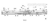
圖1是依照本發明的一實施例的一種天線模組的示意圖。請參閱圖1,在本實施例中,天線模組60包括一第一天線圖騰100及一第二天線圖騰200。第一天線圖騰100例如是LTE天線,第二天線圖騰200例如是WiFi天線,但天線模組60不以此為限制。由圖1可見,在本實施例中,天線模組60呈立體的形狀,而可減少寬度,以應用在窄邊框且尺寸有限的空間中,且可提供多頻的效果。FIG. 1 is a schematic diagram of an antenna module according to an embodiment of the present invention. Referring to FIG. 1 , in this embodiment, the
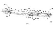
由於立體的天線模組60的形狀複雜,為了更清楚地表示,圖2是圖1的天線模組平面展開後的簡單示意圖,以方便了解輻射體之間的相對關係。圖3至圖6是圖1的天線模組設置在電子裝置的支架10上的不同角度的示意圖。Since the shape of the three-
立體的天線模組60可透過雷射直接成型(Laser Direct Structuring,LDS)技術、柔性電路板或銅箔貼附等方式形成在電子裝置(標示於圖7)的支架10(標示於圖3)上,而可沿著支架10的多個面分布。圖3顯示出支架10的下表面12。圖4顯示出支架10的第一側面14與上表面16。圖5顯示出支架10的上表面16。圖6顯示出支架10的第二側面18。在本發明實施例中,電子裝置的支架10的材質可為塑膠。The three-
請同時參閱圖1至圖6,在本實施例中,第一天線圖騰100包括一第一天線輻射體110(位置F1、A1~A3)、一第二天線輻射體120(位置A2、A4~A6)、一第三天線輻射體150(位置F1、B5、B6)、一第一接地輻射體130(位置G1、B1、B2)、一第二接地輻射體140(位置G2、B3、B4)及一第三接地輻射體170(位置G3、D1~D7)。Please refer to FIG. 1 to FIG. 6 at the same time. In this embodiment, the
如圖1所示,第一天線輻射體110(位置F1、A1~A3)、第二天線輻射體120(位置A2、A4~A6)、第三天線輻射體150(位置F1、B5、B6)、第一接地輻射體130(位置G1、B1、B2)、第二接地輻射體140(位置G2、B3、B4)及第三接地輻射體170(位置G3、D1~D7)為立體架構。As shown in FIG. 1 , the first antenna radiator 110 (positions F1, A1-A3), the second antenna radiator 120 (positions A2, A4-A6), the third antenna radiator 150 (positions F1, B5, B6), the first ground radiator 130 (positions G1, B1, B2), the second ground radiator 140 (positions G2, B3, B4) and the third ground radiator 170 (positions G3, D1-D7) are three-dimensional structures .
第一天線輻射體110(位置F1、A1~A3)包括一第一饋入端(位置F1)。第二天線輻射體120(位置A2、A4~A6)延伸自第一天線輻射體110。由圖2可知,第二天線輻射體120在位置A2、A4的區段的延伸方向(右方)相反於第一天線輻射體110在位置A2、A3的區段的延伸方向(左方)。第三天線輻射體150(位置F1、B5、B6)延伸自第一饋入端(位置F1)且遠離第二天線輻射體120而往左方延伸。The first antenna radiator 110 (positions F1, A1 to A3) includes a first feeding end (position F1). The second antenna radiator 120 (positions A2 , A4 to A6 ) extends from the
第一接地輻射體130(位置G1、B1、B2)呈倒L型,且設置於第一天線輻射體110與第二天線輻射體120旁,而與第一天線輻射體110在位置A1、A2的區段及第二天線輻射體120在位置A2、A4的區段之間存在一第一耦合間隙C1。第一接地輻射體130包括一第一接地端(位置G1)。The first ground radiator 130 (positions G1 , B1 , B2 ) is in an inverted-L shape, and is disposed beside the
第二接地輻射體140(位置G2、B3、B4)呈倒L型,且設置於第二天線輻射體120在位置A4、A5的區段旁,而與第二天線輻射體120之間存在一第二耦合間隙C2。第二接地輻射體140包括一第二接地端(位置G2)。The second ground radiator 140 (positions G2 , B3 , B4 ) has an inverted L shape, and is disposed beside the section of the
第三接地輻射體170(位置G3、D1~D7)設置於第一天線輻射體110與第二天線輻射體120旁,由圖2可見,第三接地輻射體170(位置G3、D1~D7)接近一倒U型,第一天線輻射體110與第二天線輻射體120位於倒U型內。第三接地輻射體170包括一第三接地端(位置G3)。此外,第三接地輻射體170包括位於內部的讓位孔E1、E2,用以供機構件(例如是卡勾)通過。第三接地輻射體170在讓位孔E1、E2旁的線寬約為1公厘。The third ground radiator 170 (positions G3, D1~D7) is disposed beside the
第三接地輻射體170在位置D5的區段與第一天線輻射體110在位置A2、A3的區段之間存在一第三耦合間隙C3,第三接地輻射體170在位置D、D3的區段與第二天線輻射體120在位置A5、A6的區段之間存在一第四耦合間隙C4。A third coupling gap C3 exists between the section of the
在本實施例中,第一天線輻射體110(位置F1、A1~A3)與第三接地輻射體170(位置G3、D1~D7)透過第三耦合間隙C3共振出一第一頻段及一第二頻段。第一頻段例如是698MHz,第二頻段例如是第一頻段的二倍頻,1710MHz。第四接地輻射體220在位置D6、D7的路徑為低頻延伸路徑。在一實施例中,第一天線輻射體110(位置F1、A1~A3)與第三接地輻射體170(位置G3、D1~D7)透過第三耦合間隙C3還可共振出第一頻段的三倍頻。In this embodiment, the first antenna radiator 110 (positions F1, A1-A3) and the third ground radiator 170 (positions G3, D1-D7) resonate a first frequency band and a second frequency band. The first frequency band is, for example, 698 MHz, and the second frequency band is, for example, a double frequency of the first frequency band, 1710 MHz. The paths of the
此外,第一天線輻射體110在位置A2、A3的區段的線寬可被調整以調整第二頻段(1710MHz)的阻抗匹配及共振頻率點位置。另外,第一耦合間隙C1的寬度可被調整以調整低頻的阻抗匹配。In addition, the line width of the
第一天線輻射體110的一部分(位置A1、A2)、第二天線輻射體120(位置A2、A4~A6)與第三接地輻射體170(位置G3、D1~D7)透過第四耦合間隙C4共振出一第三頻段及一第四頻段。第三頻段為960MHz,第四頻段為第三頻段的二倍頻,1900MHz。在一實施例中,第二天線輻射體120(位置A5~A6)與第三接地輻射體170(位置D2、D3)透過第四耦合間隙C4還可共振出第三頻段的三倍頻。A part of the first antenna radiator 110 (positions A1, A2), the second antenna radiator 120 (positions A2, A4-A6) and the third ground radiator 170 (positions G3, D1-D7) pass through the fourth coupling The gap C4 resonates a third frequency band and a fourth frequency band. The third frequency band is 960MHz, and the fourth frequency band is the double frequency of the third frequency band, 1900MHz. In one embodiment, the second antenna radiator 120 (positions A5 to A6 ) and the third ground radiator 170 (positions D2 and D3 ) can resonate a triple frequency of the third frequency band through the fourth coupling gap C4 .
第二天線輻射體120在位置A5、A6的區段與第三接地輻射體170在位置D2、D3的區段之間的第四耦合間隙C4的寬度以及第三接地輻射體170在位置D2、D3的區段的線寬可被調整,以調整第三頻段(960MHz)的阻抗匹配及共振頻率點位置。The width of the fourth coupling gap C4 between the section of the
第三天線輻射體150(位置F1、B5、B6)共振出一第五頻段與一第六頻段。第五頻段例如是2500MHz~2690MHz,第六頻段例如是第五頻段的二倍頻,也就是LAA高頻頻段(5500~5925MHz)。第三天線輻射體150(位置F1、B5、B6)的線寬可被調整以調整第五頻段與第六頻段的阻抗匹配。另外,第二耦合間隙C2的寬度可被調整,以調整2500MHz~2690MHz的阻抗匹配。The third antenna radiator 150 (positions F1, B5, B6) resonates a fifth frequency band and a sixth frequency band. The fifth frequency band is, for example, 2500 MHz to 2690 MHz, and the sixth frequency band is, for example, a double frequency of the fifth frequency band, that is, the LAA high frequency band (5500 to 5925 MHz). The line width of the third antenna radiator 150 (positions F1, B5, B6) can be adjusted to adjust the impedance matching of the fifth frequency band and the sixth frequency band. In addition, the width of the second coupling gap C2 can be adjusted to adjust the impedance matching between 2500MHz and 2690MHz.
此外,第一天線圖騰100更包括一第四天線輻射體160(位置B7、B8),延伸自第二天線輻射體120在位置A4的部位且位於第三接地輻射體170的位置D3、D4之間。第三接地輻射體170在位置D4處與第四天線輻射體160之間存在一第五耦合間隙C5。第五耦合間隙C5的寬度可被調整,以調整1700~2700MHz)及二倍頻的LAA高頻頻段(5150~5500MHz)的阻抗匹配。In addition, the
另外,請參閱圖3,第一天線圖騰100(LTE天線)的第一饋入端(位置F1)、第一接地端(位置G1)、第二接地端(位置G2)與第三接地端(位置G3)設置在支架10的下表面12。In addition, please refer to FIG. 3, the first feed end (position F1), the first ground end (position G1), the second ground end (position G2) and the third ground end of the first antenna totem 100 (LTE antenna) (Position G3 ) is provided on the
在本實施例中,電子裝置的電路板上可設有多個彈片(未繪示),直接抵接於第一饋入端(位置F1)、第一接地端(位置G1)、第二接地端(位置G2)與第三接地端(位置G3)。第一饋入端(位置F1)可透過彈片電性連接至射頻訊號端20。第一接地端(位置G1)則可透過彈片浮接於一系統接地面21(例如是主機板的接地面)。第二接地端(位置G2)與系統接地面21之間串接一電容22(2.2pF)。也就是說,第二接地端(位置G2)連接電容22下地。In this embodiment, a plurality of elastic pieces (not shown) may be provided on the circuit board of the electronic device, which are directly abutted against the first feeding end (position F1 ), the first grounding end (position G1 ), and the second grounding terminal (location G2) and the third ground terminal (location G3). The first feeding end (position F1 ) can be electrically connected to the radio
類似地,第三接地端(位置G3)與系統接地面21之間串接另一電容22(2.2pF),用來改善低頻的阻抗匹配。此外,第三接地端連接於一比吸收率(SAR)感測器電路25,構成一Hybrid天線。比吸收率(SAR)感測器電路25用來偵測物體遠近,當物體靠近時降低發射功率以符合SAR的測試規範。Similarly, another capacitor 22 (2.2pF) is connected in series between the third ground terminal (position G3 ) and the
在本實施例中,第一天線圖騰100的尺寸因為配置空間相當小而受到限制,比吸收率(SAR)感測器電路25設計於主機板(未繪示)上,而不設置在第一天線圖騰100上。第一天線圖騰100透過第三接地端(位置G3)、彈片連接到主機板,進而連接到比吸收率(SAR)感測器電路25。這樣將比吸收率(SAR)感測器電路25設計於主機板的設計可讓出更多空間給第一天線圖騰100運用。In the present embodiment, the size of the
因此,第一天線圖騰100(LTE天線)可藉由上述設計,而可共振出低、中、高頻的訊號,且低、中、高頻可具有良好的阻抗匹配。Therefore, the first antenna totem 100 (LTE antenna) can resonate low, medium and high frequency signals through the above design, and the low, medium and high frequencies can have good impedance matching.
此外,第二天線圖騰200(WiFi天線)包括一第五天線輻射體210(位置F2、A7、A8)及一第四接地輻射體220(位置G4、D8~D10)。第五天線輻射體210包括一第二饋入端(位置F2)。第四接地輻射體220設置於第五天線輻射體210旁,且包圍第五天線輻射體210。第四接地輻射體220包括一第四接地端(位置G4)。在本實施例中,第二天線圖騰200可共振出2400MHz~2500MHz與5150MHz~5875MHz兩頻段。In addition, the second antenna pattern 200 (WiFi antenna) includes a fifth antenna radiator 210 (positions F2, A7, A8) and a fourth ground radiator 220 (positions G4, D8-D10). The
由圖2可見,第四接地輻射體220在位置D8~D10和第三接地輻射體170在位置D1~D7處的接地路徑都是朝向圖2的左側方向(在本實施例中,左側為裝置的內側)。這樣的設計可提升第一天線圖騰100及第二天線圖騰200之間的隔離度。It can be seen from FIG. 2 that the ground paths of the
由圖4可見,第一天線圖騰100(LTE天線)與第二天線圖騰200(WiFi天線)之間存在一距離L1,距離L1約為10公厘至30公厘之間,例如是15公厘。It can be seen from FIG. 4 that there is a distance L1 between the first antenna totem 100 (LTE antenna) and the second antenna totem 200 (WiFi antenna), and the distance L1 is about 10 mm to 30 mm, for example, 15 mm. mm.
另外,圖3的左側可見,第二天線圖騰200的第二饋入端及第四接地端設置在支架10的下表面12。第二饋入端可連接於同軸傳輸線(未繪示)的正端,而接到系統訊號端。第四接地端可連接於同軸傳輸線的負端,而連接至接地面。In addition, it can be seen from the left side of FIG. 3 that the second feeding end and the fourth grounding end of the
圖7是依照本發明一實施例其一種電子裝置的局部側邊剖面示意圖,其中此剖面對應於圖5的A-A線段剖面。也就是說,圖7中所顯示的天線模組60與支架10的剖面是圖5的A-A線段剖面。請參閱圖7,在本實施例中,電子裝置1例如是一平板電腦,但不以此為限制。7 is a partial side cross-sectional schematic diagram of an electronic device according to an embodiment of the present invention, wherein the cross-section corresponds to the cross-section of the line A-A in FIG. 5 . That is, the cross-section of the
電子裝置1包括一殼體40、圖3的支架10與天線模組60(標示於圖3)及一螢幕金屬件50。殼體40包括一窄邊框區42。支架10設置於殼體40內且位於窄邊框區42。天線模組60設置於支架10的下表面12、第一側面14、上表面16及第二側面18上。螢幕金屬件50設置於殼體40內且位於天線模組60旁。The
在本實施例中,第一天線圖騰100的可用空間的長度約為79公厘,寬度L2是7.92公厘,高度L3是4.98公厘。窄邊框區42能夠提供天線模組60配置的空間有限,在本實施例中,天線模組60被設置在支架10上,而呈現立體的形式,藉此縮減寬度上的尺寸。In this embodiment, the length of the available space of the
此外,由於天線模組60(圖7中顯示第一天線圖騰100)需要與螢幕金屬件50之間存在一間距L4,間距L4要大於等於1公厘,以降低螢幕金屬件50對天線模組60造成的影響。在本實施例中,第一天線圖騰100的局部呈階梯狀,以增加與螢幕金屬件50之間的距離,而降低干擾。在本實施例中,第一天線圖騰100在與螢幕金屬件50等高處的部位(也就是階梯頂端處)與階梯底端的部位之間的橫向距離L5約為3.92公厘。因此,這樣階梯式的設計可爭取更多第一天線圖騰100與螢幕金屬件50之間的距離。In addition, since the antenna module 60 (the
另外,由於螢幕金屬件50位於支架10在第一側面14旁,第一天線圖騰100(LTE天線)設置在第一側面14旁的部分均採用階梯式的設計。具體地說,請回到圖4,第一天線輻射體110在位置A1、A2的區段、第一接地輻射體130在位置B1、B2的區段、第二接地輻射體140在位置B3、B4的區段及接地輻射體在位置D1、D2的區段均採用階梯式的設計。In addition, since the
再者,在本實施例中,電子裝置1更包括一金屬背蓋30(圖2),靠近第一天線圖騰100的第三接地輻射體170。金屬背蓋30與第三接地輻射體170之間形成一第六耦合間隙C6。第六耦合間隙C6介於0.5公厘至1公厘之間。Furthermore, in this embodiment, the
圖8是圖1的天線模組的頻率-VSWR的關係圖。請參閱圖8,在本實施例中,第一天線圖騰100在頻率為698MHz~960MHz下,VSWR可小於等於5。第一天線圖騰100與第二天線圖騰200在頻率為1710~2700MHz、3300MHz~3800MHz和5150MHz~5925MHz下,VSWR都可小於4,而具有良好的表現。FIG. 8 is a frequency-VSWR relationship diagram of the antenna module of FIG. 1 . Referring to FIG. 8 , in this embodiment, when the frequency of the
圖9是圖1的天線模組的頻率-隔離度的關係圖。請參閱圖9,在本實施例中,第一天線圖騰100與第二天線圖騰200的隔離度可小於-15dB,而具有良好的表現。FIG. 9 is a frequency-isolation relationship diagram of the antenna module of FIG. 1 . Referring to FIG. 9 , in this embodiment, the isolation between the
圖10是圖1的天線模組的頻率-天線效率的關係圖。請參閱圖10,第一天線圖騰100(LTE天線)在頻率為698MHz~960MHz下,天線效率為-5.1dBi~-7.3dBi,在頻率為1710MHz~2700MHz下,天線效率為-4.2dBi~-5.8dBi,在頻率為5150MHz~5925MHz下,天線效率為-3.6dBi~-6.0dBi,而擁有LTE寬頻天線效率的表現。FIG. 10 is a frequency-antenna efficiency relationship diagram of the antenna module of FIG. 1 . Referring to Fig. 10, the first antenna totem 100 (LTE antenna) has an antenna efficiency of -5.1dBi~-7.3dBi at a frequency of 698MHz~960MHz, and an antenna efficiency of -4.2dBi~- at a frequency of 1710MHz~2700MHz. 5.8dBi, at the frequency of 5150MHz~5925MHz, the antenna efficiency is -3.6dBi~-6.0dBi, and has the performance of LTE broadband antenna efficiency.
第二天線圖騰200(WiFi天線)在頻率為2400MHz~2500MHz下天線效率為-2.7dBi~-3.1dBi,在頻率為5150MHz~5875MHz下,天線效率為-3.0dBi~-4.3dBi,而擁有良好的表現。The antenna efficiency of the second antenna Totem 200 (WiFi antenna) is -2.7dBi~-3.1dBi at the frequency of 2400MHz~2500MHz, and the antenna efficiency is -3.0dBi~-4.3dBi at the frequency of 5150MHz~5875MHz. Performance.
綜上所述,本發明的天線模組的第二天線輻射體延伸自第一天線輻射體。第三天線輻射體自第一饋入端且朝遠離第二天線輻射體方向延伸。第一接地輻射體鄰設於第一天線輻射體與第二天線輻射體,而與第一天線輻射體及第二天線輻射體之間存在第一耦合間隙。第二接地輻射體鄰設於第二天線輻射體,而與第二天線輻射體之間存在第二耦合間隙。第三接地輻射體鄰設於第一天線輻射體與第二天線輻射體。第三接地輻射體與第一天線輻射體之間存在第三耦合間隙。第三接地輻射體與第二天線輻射體之間存在第四耦合間隙。藉由上述設計,第一天線輻射體與第三接地輻射體透過第三耦合間隙共振出第一頻段及第二頻段。第一天線輻射體的一部分、第二天線輻射體與第三接地輻射體透過第四耦合間隙共振出第三頻段及第四頻段。第三天線輻射體共振出第五頻段與第六頻段。因此,本發明的天線模組可具有多頻的特性。To sum up, the second antenna radiator of the antenna module of the present invention extends from the first antenna radiator. The third antenna radiator extends from the first feeding end in a direction away from the second antenna radiator. The first ground radiator is adjacent to the first antenna radiator and the second antenna radiator, and a first coupling gap exists between the first antenna radiator and the second antenna radiator. The second ground radiator is adjacent to the second antenna radiator, and a second coupling gap exists between the second ground radiator and the second antenna radiator. The third ground radiator is adjacent to the first antenna radiator and the second antenna radiator. A third coupling gap exists between the third ground radiator and the first antenna radiator. A fourth coupling gap exists between the third ground radiator and the second antenna radiator. With the above design, the first antenna radiator and the third ground radiator resonate out the first frequency band and the second frequency band through the third coupling gap. A part of the first antenna radiator, the second antenna radiator and the third ground radiator resonate out the third frequency band and the fourth frequency band through the fourth coupling gap. The third antenna radiator resonates the fifth frequency band and the sixth frequency band. Therefore, the antenna module of the present invention can have multi-frequency characteristics.
A1~A8、B1~B6、D1~D7、F1、F2、G1~G4:位置 C1:第一耦合間隙 C2:第二耦合間隙 C3:第三耦合間隙 C4:第四耦合間隙 C5:第五耦合間隙 C6:第六耦合間隙 E1、E2:讓位孔 L1、L5:距離 L2:寬度 L3:高度 L4:間距 1:電子裝置 10:支架 12:下表面 14:第一側面 16:上表面 18:第二側面 20:射頻訊號端 21:系統接地面 22:電容 25:比吸收率(SAR)感測器電路 30:金屬背蓋 40:殼體 42:窄邊框區 50:螢幕金屬件 60:天線模組 100:第一天線圖騰 110:第一天線輻射體 120:第二天線輻射體 130:第一接地輻射體 140:第二接地輻射體 150:第三天線輻射體 160:第四天線輻射體 170:第三接地輻射體 200:第二天線圖騰 210:第五天線輻射體 220:第四接地輻射體A1~A8, B1~B6, D1~D7, F1, F2, G1~G4: Position C1: First coupling gap C2: Second coupling gap C3: Third coupling gap C4: Fourth coupling gap C5: Fifth coupling gap C6: sixth coupling gap E1, E2: Make way for holes L1, L5: distance L2: width L3: height L4: Spacing 1: Electronic device 10: Bracket 12: Lower surface 14: The first side 16: Top surface 18: Second side 20: RF signal terminal 21: System ground plane 22: Capacitor 25: Specific Absorption Rate (SAR) Sensor Circuit 30: Metal back cover 40: Shell 42: Narrow border area 50: Screen metal parts 60: Antenna module 100: First Antenna Totem 110: The first antenna radiator 120: second antenna radiator 130: First ground radiator 140: Second ground radiator 150: The third antenna radiator 160: Fourth Antenna Radiator 170: Third ground radiator 200: Second Antenna Totem 210: Fifth Antenna Radiator 220: Fourth ground radiator
圖1是依照本發明的一實施例的一種天線模組的示意圖。 圖2是圖1的天線模組平面展開後的簡單示意圖。 圖3至圖6是圖1的天線模組設置在電子裝置的支架上的不同角度的示意圖。 圖7是依照本發明一實施例其一種電子裝置的局部側邊剖面示意圖。 圖8是圖1的天線模組的頻率-VSWR的關係圖。 圖9是圖1的天線模組的頻率-隔離度的關係圖。 圖10是圖1的天線模組的頻率-天線效率的關係圖。FIG. 1 is a schematic diagram of an antenna module according to an embodiment of the present invention. FIG. 2 is a simple schematic diagram of the antenna module of FIG. 1 after the plane is unfolded. 3 to 6 are schematic diagrams illustrating different angles of the antenna module of FIG. 1 disposed on the bracket of the electronic device. 7 is a partial side cross-sectional schematic diagram of an electronic device according to an embodiment of the present invention. FIG. 8 is a frequency-VSWR relationship diagram of the antenna module of FIG. 1 . FIG. 9 is a frequency-isolation relationship diagram of the antenna module of FIG. 1 . FIG. 10 is a frequency-antenna efficiency relationship diagram of the antenna module of FIG. 1 .
A1~A8、B1~B6、D1~D7、F1、F2、G1~G4:位置A1~A8, B1~B6, D1~D7, F1, F2, G1~G4: Position
C1:第一耦合間隙C1: First coupling gap
C2:第二耦合間隙C2: Second coupling gap
C3:第三耦合間隙C3: Third coupling gap
C4:第四耦合間隙C4: Fourth coupling gap
C5:第五耦合間隙C5: Fifth coupling gap
E1、E2:讓位孔E1, E2: Make way for holes
60:天線模組60: Antenna module
100:第一天線圖騰100: First Antenna Totem
110:第一天線輻射體110: The first antenna radiator
120:第二天線輻射體120: second antenna radiator
130:第一接地輻射體130: First ground radiator
140:第二接地輻射體140: Second ground radiator
150:第三天線輻射體150: The third antenna radiator
160:第四天線輻射體160: Fourth Antenna Radiator
170:第三接地輻射體170: Third ground radiator
200:第二天線圖騰200: Second Antenna Totem
210:第五天線輻射體210: Fifth Antenna Radiator
220:第四接地輻射體220: Fourth ground radiator
Claims (10)
Translated fromChinesePriority Applications (3)
| Application Number | Priority Date | Filing Date | Title |
|---|---|---|---|
| TW110114719ATWI768843B (en) | 2021-04-23 | 2021-04-23 | Antenna module and electronic device |
| CN202210177452.1ACN115241649B (en) | 2021-04-23 | 2022-02-25 | Antenna module and electronic device |
| US17/691,973US11843186B2 (en) | 2021-04-23 | 2022-03-10 | Antenna module and electronic device |
Applications Claiming Priority (1)
| Application Number | Priority Date | Filing Date | Title |
|---|---|---|---|
| TW110114719ATWI768843B (en) | 2021-04-23 | 2021-04-23 | Antenna module and electronic device |
Publications (2)
| Publication Number | Publication Date |
|---|---|
| TWI768843Btrue TWI768843B (en) | 2022-06-21 |
| TW202243327A TW202243327A (en) | 2022-11-01 |
Family
ID=83103978
Family Applications (1)
| Application Number | Title | Priority Date | Filing Date |
|---|---|---|---|
| TW110114719ATWI768843B (en) | 2021-04-23 | 2021-04-23 | Antenna module and electronic device |
Country Status (3)
| Country | Link |
|---|---|
| US (1) | US11843186B2 (en) |
| CN (1) | CN115241649B (en) |
| TW (1) | TWI768843B (en) |
Cited By (1)
| Publication number | Priority date | Publication date | Assignee | Title |
|---|---|---|---|---|
| TWI811088B (en)* | 2022-09-02 | 2023-08-01 | 和碩聯合科技股份有限公司 | Electronic device |
Families Citing this family (5)
| Publication number | Priority date | Publication date | Assignee | Title |
|---|---|---|---|---|
| CN111555019B (en)* | 2020-05-20 | 2022-07-12 | 维沃移动通信有限公司 | Electronic equipment |
| TWI775384B (en)* | 2021-04-13 | 2022-08-21 | 和碩聯合科技股份有限公司 | Antenna module and electronic device |
| TWI782657B (en)* | 2021-08-06 | 2022-11-01 | 和碩聯合科技股份有限公司 | Antenna module |
| TWI792570B (en)* | 2021-09-17 | 2023-02-11 | 和碩聯合科技股份有限公司 | Electronic device |
| TWI850855B (en)* | 2022-11-17 | 2024-08-01 | 宏碁股份有限公司 | Mobile device supporting wideband operation |
Citations (4)
| Publication number | Priority date | Publication date | Assignee | Title |
|---|---|---|---|---|
| US20100019974A1 (en)* | 2007-07-24 | 2010-01-28 | Hon Hai Precision Ind. Co., Ltd. | Multi-band antenna |
| TWM393815U (en)* | 2010-05-18 | 2010-12-01 | Hon Hai Prec Ind Co Ltd | Antenna assembly |
| US20100315294A1 (en)* | 2009-06-11 | 2010-12-16 | Pao-Sui Chang | Integrated multi-band antenna module |
| US20120050111A1 (en)* | 2010-08-26 | 2012-03-01 | Hon Hai Precision Industry Co., Ltd. | Multi-band combined antenna |
Family Cites Families (9)
| Publication number | Priority date | Publication date | Assignee | Title |
|---|---|---|---|---|
| US7394430B2 (en)* | 2001-04-11 | 2008-07-01 | Kyocera Wireless Corp. | Wireless device reconfigurable radiation desensitivity bracket systems and methods |
| US7439914B1 (en) | 2007-04-27 | 2008-10-21 | Cheng Uei Precision Industry Co., Ltd. | Antenna unit |
| US8970436B2 (en)* | 2013-03-14 | 2015-03-03 | Circomm Technology Corp. | Surface mount device multi-frequency antenna module |
| US9973228B2 (en)* | 2014-08-26 | 2018-05-15 | Pulse Finland Oy | Antenna apparatus with an integrated proximity sensor and methods |
| TWI569513B (en)* | 2015-12-03 | 2017-02-01 | 和碩聯合科技股份有限公司 | Antenna module |
| TWI628865B (en)* | 2017-03-24 | 2018-07-01 | 和碩聯合科技股份有限公司 | Antenna structure and electronic device |
| CN112186334B (en)* | 2019-07-03 | 2023-05-02 | 亚旭电脑股份有限公司 | Multi-frequency antenna module |
| CN112531331B (en)* | 2019-09-18 | 2022-04-12 | 华为技术有限公司 | Antenna and terminal equipment |
| CN111641028B (en) | 2020-05-09 | 2022-08-12 | 东莞职业技术学院 | Dual-polarized antenna structure and wireless communication device thereof |
- 2021
- 2021-04-23TWTW110114719Apatent/TWI768843B/enactive
- 2022
- 2022-02-25CNCN202210177452.1Apatent/CN115241649B/enactiveActive
- 2022-03-10USUS17/691,973patent/US11843186B2/enactiveActive
Patent Citations (4)
| Publication number | Priority date | Publication date | Assignee | Title |
|---|---|---|---|---|
| US20100019974A1 (en)* | 2007-07-24 | 2010-01-28 | Hon Hai Precision Ind. Co., Ltd. | Multi-band antenna |
| US20100315294A1 (en)* | 2009-06-11 | 2010-12-16 | Pao-Sui Chang | Integrated multi-band antenna module |
| TWM393815U (en)* | 2010-05-18 | 2010-12-01 | Hon Hai Prec Ind Co Ltd | Antenna assembly |
| US20120050111A1 (en)* | 2010-08-26 | 2012-03-01 | Hon Hai Precision Industry Co., Ltd. | Multi-band combined antenna |
Cited By (1)
| Publication number | Priority date | Publication date | Assignee | Title |
|---|---|---|---|---|
| TWI811088B (en)* | 2022-09-02 | 2023-08-01 | 和碩聯合科技股份有限公司 | Electronic device |
Also Published As
| Publication number | Publication date |
|---|---|
| US20220344814A1 (en) | 2022-10-27 |
| TW202243327A (en) | 2022-11-01 |
| CN115241649B (en) | 2025-08-01 |
| CN115241649A (en) | 2022-10-25 |
| US11843186B2 (en) | 2023-12-12 |
Similar Documents
| Publication | Publication Date | Title |
|---|---|---|
| TWI768843B (en) | Antenna module and electronic device | |
| TWI476989B (en) | Multi-band antenna | |
| TWI478437B (en) | Antenna module and portable electronic device employing the same | |
| CN111193104B (en) | Dual frequency antenna device | |
| US11581650B2 (en) | Multi-input multi-output antenna structure | |
| US10938100B2 (en) | Dual-feed loop antenna structure and electronic device | |
| WO2005076933A2 (en) | Slotted multiple band antenna | |
| TWI782657B (en) | Antenna module | |
| TWI734469B (en) | Electronic device and antenna module | |
| TWI559615B (en) | Multi-band antenna | |
| CN101997162A (en) | Multi-frequency antenna | |
| TW202036986A (en) | Dual-band antenna | |
| US12113292B2 (en) | Antenna device | |
| CN103840255B (en) | Printing type broadband monopole antenna module | |
| CN112635973B (en) | Antenna structure and communication device | |
| TW202410543A (en) | Electronic device | |
| CN111384588B (en) | Multi-frequency antenna | |
| TWI530025B (en) | Multiband antenna for portable electronic device | |
| CN1964132B (en) | Hidden Multi-Band Antennas for Portable Devices | |
| TWI528631B (en) | Planar inverted f antenna | |
| TW201721968A (en) | Antenna and electric device using the same | |
| CN106033834A (en) | antenna structure | |
| US12191557B2 (en) | Electronic device | |
| US12438253B2 (en) | Wireless dongle | |
| CN101540429A (en) | Antenna for global positioning system |