TWI768294B - Package structure and manufacturing method thereof - Google Patents
Package structure and manufacturing method thereofDownload PDFInfo
- Publication number
- TWI768294B TWI768294BTW109106328ATW109106328ATWI768294BTW I768294 BTWI768294 BTW I768294BTW 109106328 ATW109106328 ATW 109106328ATW 109106328 ATW109106328 ATW 109106328ATW I768294 BTWI768294 BTW I768294B
- Authority
- TW
- Taiwan
- Prior art keywords
- chip
- active
- tsv
- bridge
- silicon
- Prior art date
Links
Images


Classifications
- H—ELECTRICITY
- H01—ELECTRIC ELEMENTS
- H01L—SEMICONDUCTOR DEVICES NOT COVERED BY CLASS H10
- H01L22/00—Testing or measuring during manufacture or treatment; Reliability measurements, i.e. testing of parts without further processing to modify the parts as such; Structural arrangements therefor
- H01L22/30—Structural arrangements specially adapted for testing or measuring during manufacture or treatment, or specially adapted for reliability measurements
- H01L22/32—Additional lead-in metallisation on a device or substrate, e.g. additional pads or pad portions, lines in the scribe line, sacrificed conductors
- H—ELECTRICITY
- H01—ELECTRIC ELEMENTS
- H01L—SEMICONDUCTOR DEVICES NOT COVERED BY CLASS H10
- H01L23/00—Details of semiconductor or other solid state devices
- H01L23/52—Arrangements for conducting electric current within the device in operation from one component to another, i.e. interconnections, e.g. wires, lead frames
- H01L23/538—Arrangements for conducting electric current within the device in operation from one component to another, i.e. interconnections, e.g. wires, lead frames the interconnection structure between a plurality of semiconductor chips being formed on, or in, insulating substrates
- H01L23/5389—Arrangements for conducting electric current within the device in operation from one component to another, i.e. interconnections, e.g. wires, lead frames the interconnection structure between a plurality of semiconductor chips being formed on, or in, insulating substrates the chips being integrally enclosed by the interconnect and support structures
- H—ELECTRICITY
- H01—ELECTRIC ELEMENTS
- H01L—SEMICONDUCTOR DEVICES NOT COVERED BY CLASS H10
- H01L23/00—Details of semiconductor or other solid state devices
- H01L23/48—Arrangements for conducting electric current to or from the solid state body in operation, e.g. leads, terminal arrangements ; Selection of materials therefor
- H01L23/488—Arrangements for conducting electric current to or from the solid state body in operation, e.g. leads, terminal arrangements ; Selection of materials therefor consisting of soldered or bonded constructions
- H01L23/498—Leads, i.e. metallisations or lead-frames on insulating substrates, e.g. chip carriers
- H01L23/49838—Geometry or layout
- H—ELECTRICITY
- H01—ELECTRIC ELEMENTS
- H01L—SEMICONDUCTOR DEVICES NOT COVERED BY CLASS H10
- H01L21/00—Processes or apparatus adapted for the manufacture or treatment of semiconductor or solid state devices or of parts thereof
- H01L21/02—Manufacture or treatment of semiconductor devices or of parts thereof
- H01L21/04—Manufacture or treatment of semiconductor devices or of parts thereof the devices having potential barriers, e.g. a PN junction, depletion layer or carrier concentration layer
- H01L21/48—Manufacture or treatment of parts, e.g. containers, prior to assembly of the devices, using processes not provided for in a single one of the groups H01L21/18 - H01L21/326 or H10D48/04 - H10D48/07
- H01L21/4803—Insulating or insulated parts, e.g. mountings, containers, diamond heatsinks
- H01L21/481—Insulating layers on insulating parts, with or without metallisation
- H—ELECTRICITY
- H01—ELECTRIC ELEMENTS
- H01L—SEMICONDUCTOR DEVICES NOT COVERED BY CLASS H10
- H01L21/00—Processes or apparatus adapted for the manufacture or treatment of semiconductor or solid state devices or of parts thereof
- H01L21/02—Manufacture or treatment of semiconductor devices or of parts thereof
- H01L21/04—Manufacture or treatment of semiconductor devices or of parts thereof the devices having potential barriers, e.g. a PN junction, depletion layer or carrier concentration layer
- H01L21/48—Manufacture or treatment of parts, e.g. containers, prior to assembly of the devices, using processes not provided for in a single one of the groups H01L21/18 - H01L21/326 or H10D48/04 - H10D48/07
- H01L21/4814—Conductive parts
- H01L21/4846—Leads on or in insulating or insulated substrates, e.g. metallisation
- H01L21/4853—Connection or disconnection of other leads to or from a metallisation, e.g. pins, wires, bumps
- H—ELECTRICITY
- H01—ELECTRIC ELEMENTS
- H01L—SEMICONDUCTOR DEVICES NOT COVERED BY CLASS H10
- H01L21/00—Processes or apparatus adapted for the manufacture or treatment of semiconductor or solid state devices or of parts thereof
- H01L21/02—Manufacture or treatment of semiconductor devices or of parts thereof
- H01L21/04—Manufacture or treatment of semiconductor devices or of parts thereof the devices having potential barriers, e.g. a PN junction, depletion layer or carrier concentration layer
- H01L21/48—Manufacture or treatment of parts, e.g. containers, prior to assembly of the devices, using processes not provided for in a single one of the groups H01L21/18 - H01L21/326 or H10D48/04 - H10D48/07
- H01L21/4814—Conductive parts
- H01L21/4846—Leads on or in insulating or insulated substrates, e.g. metallisation
- H01L21/4857—Multilayer substrates
- H—ELECTRICITY
- H01—ELECTRIC ELEMENTS
- H01L—SEMICONDUCTOR DEVICES NOT COVERED BY CLASS H10
- H01L21/00—Processes or apparatus adapted for the manufacture or treatment of semiconductor or solid state devices or of parts thereof
- H01L21/02—Manufacture or treatment of semiconductor devices or of parts thereof
- H01L21/04—Manufacture or treatment of semiconductor devices or of parts thereof the devices having potential barriers, e.g. a PN junction, depletion layer or carrier concentration layer
- H01L21/50—Assembly of semiconductor devices using processes or apparatus not provided for in a single one of the groups H01L21/18 - H01L21/326 or H10D48/04 - H10D48/07 e.g. sealing of a cap to a base of a container
- H01L21/56—Encapsulations, e.g. encapsulation layers, coatings
- H01L21/561—Batch processing
- H—ELECTRICITY
- H01—ELECTRIC ELEMENTS
- H01L—SEMICONDUCTOR DEVICES NOT COVERED BY CLASS H10
- H01L21/00—Processes or apparatus adapted for the manufacture or treatment of semiconductor or solid state devices or of parts thereof
- H01L21/02—Manufacture or treatment of semiconductor devices or of parts thereof
- H01L21/04—Manufacture or treatment of semiconductor devices or of parts thereof the devices having potential barriers, e.g. a PN junction, depletion layer or carrier concentration layer
- H01L21/50—Assembly of semiconductor devices using processes or apparatus not provided for in a single one of the groups H01L21/18 - H01L21/326 or H10D48/04 - H10D48/07 e.g. sealing of a cap to a base of a container
- H01L21/56—Encapsulations, e.g. encapsulation layers, coatings
- H01L21/565—Moulds
- H—ELECTRICITY
- H01—ELECTRIC ELEMENTS
- H01L—SEMICONDUCTOR DEVICES NOT COVERED BY CLASS H10
- H01L21/00—Processes or apparatus adapted for the manufacture or treatment of semiconductor or solid state devices or of parts thereof
- H01L21/02—Manufacture or treatment of semiconductor devices or of parts thereof
- H01L21/04—Manufacture or treatment of semiconductor devices or of parts thereof the devices having potential barriers, e.g. a PN junction, depletion layer or carrier concentration layer
- H01L21/50—Assembly of semiconductor devices using processes or apparatus not provided for in a single one of the groups H01L21/18 - H01L21/326 or H10D48/04 - H10D48/07 e.g. sealing of a cap to a base of a container
- H01L21/56—Encapsulations, e.g. encapsulation layers, coatings
- H01L21/568—Temporary substrate used as encapsulation process aid
- H—ELECTRICITY
- H01—ELECTRIC ELEMENTS
- H01L—SEMICONDUCTOR DEVICES NOT COVERED BY CLASS H10
- H01L21/00—Processes or apparatus adapted for the manufacture or treatment of semiconductor or solid state devices or of parts thereof
- H01L21/67—Apparatus specially adapted for handling semiconductor or electric solid state devices during manufacture or treatment thereof; Apparatus specially adapted for handling wafers during manufacture or treatment of semiconductor or electric solid state devices or components ; Apparatus not specifically provided for elsewhere
- H01L21/683—Apparatus specially adapted for handling semiconductor or electric solid state devices during manufacture or treatment thereof; Apparatus specially adapted for handling wafers during manufacture or treatment of semiconductor or electric solid state devices or components ; Apparatus not specifically provided for elsewhere for supporting or gripping
- H01L21/6835—Apparatus specially adapted for handling semiconductor or electric solid state devices during manufacture or treatment thereof; Apparatus specially adapted for handling wafers during manufacture or treatment of semiconductor or electric solid state devices or components ; Apparatus not specifically provided for elsewhere for supporting or gripping using temporarily an auxiliary support
- H—ELECTRICITY
- H01—ELECTRIC ELEMENTS
- H01L—SEMICONDUCTOR DEVICES NOT COVERED BY CLASS H10
- H01L21/00—Processes or apparatus adapted for the manufacture or treatment of semiconductor or solid state devices or of parts thereof
- H01L21/70—Manufacture or treatment of devices consisting of a plurality of solid state components formed in or on a common substrate or of parts thereof; Manufacture of integrated circuit devices or of parts thereof
- H01L21/77—Manufacture or treatment of devices consisting of a plurality of solid state components or integrated circuits formed in, or on, a common substrate
- H01L21/78—Manufacture or treatment of devices consisting of a plurality of solid state components or integrated circuits formed in, or on, a common substrate with subsequent division of the substrate into plural individual devices
- H—ELECTRICITY
- H01—ELECTRIC ELEMENTS
- H01L—SEMICONDUCTOR DEVICES NOT COVERED BY CLASS H10
- H01L23/00—Details of semiconductor or other solid state devices
- H01L23/16—Fillings or auxiliary members in containers or encapsulations, e.g. centering rings
- H—ELECTRICITY
- H01—ELECTRIC ELEMENTS
- H01L—SEMICONDUCTOR DEVICES NOT COVERED BY CLASS H10
- H01L23/00—Details of semiconductor or other solid state devices
- H01L23/16—Fillings or auxiliary members in containers or encapsulations, e.g. centering rings
- H01L23/18—Fillings characterised by the material, its physical or chemical properties, or its arrangement within the complete device
- H01L23/24—Fillings characterised by the material, its physical or chemical properties, or its arrangement within the complete device solid or gel at the normal operating temperature of the device
- H—ELECTRICITY
- H01—ELECTRIC ELEMENTS
- H01L—SEMICONDUCTOR DEVICES NOT COVERED BY CLASS H10
- H01L23/00—Details of semiconductor or other solid state devices
- H01L23/28—Encapsulations, e.g. encapsulating layers, coatings, e.g. for protection
- H01L23/31—Encapsulations, e.g. encapsulating layers, coatings, e.g. for protection characterised by the arrangement or shape
- H01L23/3107—Encapsulations, e.g. encapsulating layers, coatings, e.g. for protection characterised by the arrangement or shape the device being completely enclosed
- H01L23/3121—Encapsulations, e.g. encapsulating layers, coatings, e.g. for protection characterised by the arrangement or shape the device being completely enclosed a substrate forming part of the encapsulation
- H01L23/3128—Encapsulations, e.g. encapsulating layers, coatings, e.g. for protection characterised by the arrangement or shape the device being completely enclosed a substrate forming part of the encapsulation the substrate having spherical bumps for external connection
- H—ELECTRICITY
- H01—ELECTRIC ELEMENTS
- H01L—SEMICONDUCTOR DEVICES NOT COVERED BY CLASS H10
- H01L23/00—Details of semiconductor or other solid state devices
- H01L23/34—Arrangements for cooling, heating, ventilating or temperature compensation ; Temperature sensing arrangements
- H01L23/36—Selection of materials, or shaping, to facilitate cooling or heating, e.g. heatsinks
- H01L23/367—Cooling facilitated by shape of device
- H01L23/3675—Cooling facilitated by shape of device characterised by the shape of the housing
- H—ELECTRICITY
- H01—ELECTRIC ELEMENTS
- H01L—SEMICONDUCTOR DEVICES NOT COVERED BY CLASS H10
- H01L23/00—Details of semiconductor or other solid state devices
- H01L23/48—Arrangements for conducting electric current to or from the solid state body in operation, e.g. leads, terminal arrangements ; Selection of materials therefor
- H01L23/482—Arrangements for conducting electric current to or from the solid state body in operation, e.g. leads, terminal arrangements ; Selection of materials therefor consisting of lead-in layers inseparably applied to the semiconductor body (electrodes)
- H01L23/4824—Pads with extended contours, e.g. grid structure, branch structure, finger structure
- H—ELECTRICITY
- H01—ELECTRIC ELEMENTS
- H01L—SEMICONDUCTOR DEVICES NOT COVERED BY CLASS H10
- H01L23/00—Details of semiconductor or other solid state devices
- H01L23/48—Arrangements for conducting electric current to or from the solid state body in operation, e.g. leads, terminal arrangements ; Selection of materials therefor
- H01L23/488—Arrangements for conducting electric current to or from the solid state body in operation, e.g. leads, terminal arrangements ; Selection of materials therefor consisting of soldered or bonded constructions
- H01L23/498—Leads, i.e. metallisations or lead-frames on insulating substrates, e.g. chip carriers
- H01L23/49811—Additional leads joined to the metallisation on the insulating substrate, e.g. pins, bumps, wires, flat leads
- H01L23/49816—Spherical bumps on the substrate for external connection, e.g. ball grid arrays [BGA]
- H—ELECTRICITY
- H01—ELECTRIC ELEMENTS
- H01L—SEMICONDUCTOR DEVICES NOT COVERED BY CLASS H10
- H01L23/00—Details of semiconductor or other solid state devices
- H01L23/48—Arrangements for conducting electric current to or from the solid state body in operation, e.g. leads, terminal arrangements ; Selection of materials therefor
- H01L23/488—Arrangements for conducting electric current to or from the solid state body in operation, e.g. leads, terminal arrangements ; Selection of materials therefor consisting of soldered or bonded constructions
- H01L23/498—Leads, i.e. metallisations or lead-frames on insulating substrates, e.g. chip carriers
- H01L23/49822—Multilayer substrates
- H—ELECTRICITY
- H01—ELECTRIC ELEMENTS
- H01L—SEMICONDUCTOR DEVICES NOT COVERED BY CLASS H10
- H01L23/00—Details of semiconductor or other solid state devices
- H01L23/48—Arrangements for conducting electric current to or from the solid state body in operation, e.g. leads, terminal arrangements ; Selection of materials therefor
- H01L23/488—Arrangements for conducting electric current to or from the solid state body in operation, e.g. leads, terminal arrangements ; Selection of materials therefor consisting of soldered or bonded constructions
- H01L23/498—Leads, i.e. metallisations or lead-frames on insulating substrates, e.g. chip carriers
- H01L23/49833—Leads, i.e. metallisations or lead-frames on insulating substrates, e.g. chip carriers the chip support structure consisting of a plurality of insulating substrates
- H—ELECTRICITY
- H01—ELECTRIC ELEMENTS
- H01L—SEMICONDUCTOR DEVICES NOT COVERED BY CLASS H10
- H01L23/00—Details of semiconductor or other solid state devices
- H01L23/52—Arrangements for conducting electric current within the device in operation from one component to another, i.e. interconnections, e.g. wires, lead frames
- H01L23/538—Arrangements for conducting electric current within the device in operation from one component to another, i.e. interconnections, e.g. wires, lead frames the interconnection structure between a plurality of semiconductor chips being formed on, or in, insulating substrates
- H01L23/5385—Assembly of a plurality of insulating substrates
- H—ELECTRICITY
- H01—ELECTRIC ELEMENTS
- H01L—SEMICONDUCTOR DEVICES NOT COVERED BY CLASS H10
- H01L23/00—Details of semiconductor or other solid state devices
- H01L23/52—Arrangements for conducting electric current within the device in operation from one component to another, i.e. interconnections, e.g. wires, lead frames
- H01L23/538—Arrangements for conducting electric current within the device in operation from one component to another, i.e. interconnections, e.g. wires, lead frames the interconnection structure between a plurality of semiconductor chips being formed on, or in, insulating substrates
- H01L23/5386—Geometry or layout of the interconnection structure
- H—ELECTRICITY
- H01—ELECTRIC ELEMENTS
- H01L—SEMICONDUCTOR DEVICES NOT COVERED BY CLASS H10
- H01L23/00—Details of semiconductor or other solid state devices
- H01L23/562—Protection against mechanical damage
- H—ELECTRICITY
- H01—ELECTRIC ELEMENTS
- H01L—SEMICONDUCTOR DEVICES NOT COVERED BY CLASS H10
- H01L24/00—Arrangements for connecting or disconnecting semiconductor or solid-state bodies; Methods or apparatus related thereto
- H01L24/01—Means for bonding being attached to, or being formed on, the surface to be connected, e.g. chip-to-package, die-attach, "first-level" interconnects; Manufacturing methods related thereto
- H01L24/02—Bonding areas ; Manufacturing methods related thereto
- H01L24/03—Manufacturing methods
- H—ELECTRICITY
- H01—ELECTRIC ELEMENTS
- H01L—SEMICONDUCTOR DEVICES NOT COVERED BY CLASS H10
- H01L24/00—Arrangements for connecting or disconnecting semiconductor or solid-state bodies; Methods or apparatus related thereto
- H01L24/01—Means for bonding being attached to, or being formed on, the surface to be connected, e.g. chip-to-package, die-attach, "first-level" interconnects; Manufacturing methods related thereto
- H01L24/02—Bonding areas ; Manufacturing methods related thereto
- H01L24/04—Structure, shape, material or disposition of the bonding areas prior to the connecting process
- H01L24/05—Structure, shape, material or disposition of the bonding areas prior to the connecting process of an individual bonding area
- H—ELECTRICITY
- H01—ELECTRIC ELEMENTS
- H01L—SEMICONDUCTOR DEVICES NOT COVERED BY CLASS H10
- H01L24/00—Arrangements for connecting or disconnecting semiconductor or solid-state bodies; Methods or apparatus related thereto
- H01L24/01—Means for bonding being attached to, or being formed on, the surface to be connected, e.g. chip-to-package, die-attach, "first-level" interconnects; Manufacturing methods related thereto
- H01L24/10—Bump connectors ; Manufacturing methods related thereto
- H01L24/12—Structure, shape, material or disposition of the bump connectors prior to the connecting process
- H01L24/14—Structure, shape, material or disposition of the bump connectors prior to the connecting process of a plurality of bump connectors
- H—ELECTRICITY
- H01—ELECTRIC ELEMENTS
- H01L—SEMICONDUCTOR DEVICES NOT COVERED BY CLASS H10
- H01L24/00—Arrangements for connecting or disconnecting semiconductor or solid-state bodies; Methods or apparatus related thereto
- H01L24/01—Means for bonding being attached to, or being formed on, the surface to be connected, e.g. chip-to-package, die-attach, "first-level" interconnects; Manufacturing methods related thereto
- H01L24/10—Bump connectors ; Manufacturing methods related thereto
- H01L24/15—Structure, shape, material or disposition of the bump connectors after the connecting process
- H01L24/16—Structure, shape, material or disposition of the bump connectors after the connecting process of an individual bump connector
- H—ELECTRICITY
- H01—ELECTRIC ELEMENTS
- H01L—SEMICONDUCTOR DEVICES NOT COVERED BY CLASS H10
- H01L24/00—Arrangements for connecting or disconnecting semiconductor or solid-state bodies; Methods or apparatus related thereto
- H01L24/01—Means for bonding being attached to, or being formed on, the surface to be connected, e.g. chip-to-package, die-attach, "first-level" interconnects; Manufacturing methods related thereto
- H01L24/10—Bump connectors ; Manufacturing methods related thereto
- H01L24/15—Structure, shape, material or disposition of the bump connectors after the connecting process
- H01L24/17—Structure, shape, material or disposition of the bump connectors after the connecting process of a plurality of bump connectors
- H—ELECTRICITY
- H01—ELECTRIC ELEMENTS
- H01L—SEMICONDUCTOR DEVICES NOT COVERED BY CLASS H10
- H01L24/00—Arrangements for connecting or disconnecting semiconductor or solid-state bodies; Methods or apparatus related thereto
- H01L24/01—Means for bonding being attached to, or being formed on, the surface to be connected, e.g. chip-to-package, die-attach, "first-level" interconnects; Manufacturing methods related thereto
- H01L24/18—High density interconnect [HDI] connectors; Manufacturing methods related thereto
- H01L24/19—Manufacturing methods of high density interconnect preforms
- H—ELECTRICITY
- H01—ELECTRIC ELEMENTS
- H01L—SEMICONDUCTOR DEVICES NOT COVERED BY CLASS H10
- H01L24/00—Arrangements for connecting or disconnecting semiconductor or solid-state bodies; Methods or apparatus related thereto
- H01L24/01—Means for bonding being attached to, or being formed on, the surface to be connected, e.g. chip-to-package, die-attach, "first-level" interconnects; Manufacturing methods related thereto
- H01L24/18—High density interconnect [HDI] connectors; Manufacturing methods related thereto
- H01L24/20—Structure, shape, material or disposition of high density interconnect preforms
- H—ELECTRICITY
- H01—ELECTRIC ELEMENTS
- H01L—SEMICONDUCTOR DEVICES NOT COVERED BY CLASS H10
- H01L24/00—Arrangements for connecting or disconnecting semiconductor or solid-state bodies; Methods or apparatus related thereto
- H01L24/93—Batch processes
- H01L24/95—Batch processes at chip-level, i.e. with connecting carried out on a plurality of singulated devices, i.e. on diced chips
- H01L24/96—Batch processes at chip-level, i.e. with connecting carried out on a plurality of singulated devices, i.e. on diced chips the devices being encapsulated in a common layer, e.g. neo-wafer or pseudo-wafer, said common layer being separable into individual assemblies after connecting
- H—ELECTRICITY
- H01—ELECTRIC ELEMENTS
- H01L—SEMICONDUCTOR DEVICES NOT COVERED BY CLASS H10
- H01L24/00—Arrangements for connecting or disconnecting semiconductor or solid-state bodies; Methods or apparatus related thereto
- H01L24/93—Batch processes
- H01L24/95—Batch processes at chip-level, i.e. with connecting carried out on a plurality of singulated devices, i.e. on diced chips
- H01L24/97—Batch processes at chip-level, i.e. with connecting carried out on a plurality of singulated devices, i.e. on diced chips the devices being connected to a common substrate, e.g. interposer, said common substrate being separable into individual assemblies after connecting
- H—ELECTRICITY
- H01—ELECTRIC ELEMENTS
- H01L—SEMICONDUCTOR DEVICES NOT COVERED BY CLASS H10
- H01L25/00—Assemblies consisting of a plurality of semiconductor or other solid state devices
- H01L25/03—Assemblies consisting of a plurality of semiconductor or other solid state devices all the devices being of a type provided for in a single subclass of subclasses H10B, H10D, H10F, H10H, H10K or H10N, e.g. assemblies of rectifier diodes
- H01L25/04—Assemblies consisting of a plurality of semiconductor or other solid state devices all the devices being of a type provided for in a single subclass of subclasses H10B, H10D, H10F, H10H, H10K or H10N, e.g. assemblies of rectifier diodes the devices not having separate containers
- H01L25/065—Assemblies consisting of a plurality of semiconductor or other solid state devices all the devices being of a type provided for in a single subclass of subclasses H10B, H10D, H10F, H10H, H10K or H10N, e.g. assemblies of rectifier diodes the devices not having separate containers the devices being of a type provided for in group H10D89/00
- H01L25/0652—Assemblies consisting of a plurality of semiconductor or other solid state devices all the devices being of a type provided for in a single subclass of subclasses H10B, H10D, H10F, H10H, H10K or H10N, e.g. assemblies of rectifier diodes the devices not having separate containers the devices being of a type provided for in group H10D89/00 the devices being arranged next and on each other, i.e. mixed assemblies
- H—ELECTRICITY
- H01—ELECTRIC ELEMENTS
- H01L—SEMICONDUCTOR DEVICES NOT COVERED BY CLASS H10
- H01L25/00—Assemblies consisting of a plurality of semiconductor or other solid state devices
- H01L25/03—Assemblies consisting of a plurality of semiconductor or other solid state devices all the devices being of a type provided for in a single subclass of subclasses H10B, H10D, H10F, H10H, H10K or H10N, e.g. assemblies of rectifier diodes
- H01L25/04—Assemblies consisting of a plurality of semiconductor or other solid state devices all the devices being of a type provided for in a single subclass of subclasses H10B, H10D, H10F, H10H, H10K or H10N, e.g. assemblies of rectifier diodes the devices not having separate containers
- H01L25/065—Assemblies consisting of a plurality of semiconductor or other solid state devices all the devices being of a type provided for in a single subclass of subclasses H10B, H10D, H10F, H10H, H10K or H10N, e.g. assemblies of rectifier diodes the devices not having separate containers the devices being of a type provided for in group H10D89/00
- H01L25/0655—Assemblies consisting of a plurality of semiconductor or other solid state devices all the devices being of a type provided for in a single subclass of subclasses H10B, H10D, H10F, H10H, H10K or H10N, e.g. assemblies of rectifier diodes the devices not having separate containers the devices being of a type provided for in group H10D89/00 the devices being arranged next to each other
- H—ELECTRICITY
- H01—ELECTRIC ELEMENTS
- H01L—SEMICONDUCTOR DEVICES NOT COVERED BY CLASS H10
- H01L25/00—Assemblies consisting of a plurality of semiconductor or other solid state devices
- H01L25/16—Assemblies consisting of a plurality of semiconductor or other solid state devices the devices being of types provided for in two or more different subclasses of H10B, H10D, H10F, H10H, H10K or H10N, e.g. forming hybrid circuits
- H—ELECTRICITY
- H01—ELECTRIC ELEMENTS
- H01L—SEMICONDUCTOR DEVICES NOT COVERED BY CLASS H10
- H01L25/00—Assemblies consisting of a plurality of semiconductor or other solid state devices
- H01L25/18—Assemblies consisting of a plurality of semiconductor or other solid state devices the devices being of the types provided for in two or more different main groups of the same subclass of H10B, H10D, H10F, H10H, H10K or H10N
- H—ELECTRICITY
- H01—ELECTRIC ELEMENTS
- H01L—SEMICONDUCTOR DEVICES NOT COVERED BY CLASS H10
- H01L25/00—Assemblies consisting of a plurality of semiconductor or other solid state devices
- H01L25/50—Multistep manufacturing processes of assemblies consisting of devices, the devices being individual devices of subclass H10D or integrated devices of class H10
- H—ELECTRICITY
- H01—ELECTRIC ELEMENTS
- H01L—SEMICONDUCTOR DEVICES NOT COVERED BY CLASS H10
- H01L2221/00—Processes or apparatus adapted for the manufacture or treatment of semiconductor or solid state devices or of parts thereof covered by H01L21/00
- H01L2221/67—Apparatus for handling semiconductor or electric solid state devices during manufacture or treatment thereof; Apparatus for handling wafers during manufacture or treatment of semiconductor or electric solid state devices or components; Apparatus not specifically provided for elsewhere
- H01L2221/683—Apparatus for handling semiconductor or electric solid state devices during manufacture or treatment thereof; Apparatus for handling wafers during manufacture or treatment of semiconductor or electric solid state devices or components; Apparatus not specifically provided for elsewhere for supporting or gripping
- H01L2221/68304—Apparatus for handling semiconductor or electric solid state devices during manufacture or treatment thereof; Apparatus for handling wafers during manufacture or treatment of semiconductor or electric solid state devices or components; Apparatus not specifically provided for elsewhere for supporting or gripping using temporarily an auxiliary support
- H01L2221/68345—Apparatus for handling semiconductor or electric solid state devices during manufacture or treatment thereof; Apparatus for handling wafers during manufacture or treatment of semiconductor or electric solid state devices or components; Apparatus not specifically provided for elsewhere for supporting or gripping using temporarily an auxiliary support used as a support during the manufacture of self supporting substrates
- H—ELECTRICITY
- H01—ELECTRIC ELEMENTS
- H01L—SEMICONDUCTOR DEVICES NOT COVERED BY CLASS H10
- H01L2221/00—Processes or apparatus adapted for the manufacture or treatment of semiconductor or solid state devices or of parts thereof covered by H01L21/00
- H01L2221/67—Apparatus for handling semiconductor or electric solid state devices during manufacture or treatment thereof; Apparatus for handling wafers during manufacture or treatment of semiconductor or electric solid state devices or components; Apparatus not specifically provided for elsewhere
- H01L2221/683—Apparatus for handling semiconductor or electric solid state devices during manufacture or treatment thereof; Apparatus for handling wafers during manufacture or treatment of semiconductor or electric solid state devices or components; Apparatus not specifically provided for elsewhere for supporting or gripping
- H01L2221/68304—Apparatus for handling semiconductor or electric solid state devices during manufacture or treatment thereof; Apparatus for handling wafers during manufacture or treatment of semiconductor or electric solid state devices or components; Apparatus not specifically provided for elsewhere for supporting or gripping using temporarily an auxiliary support
- H01L2221/68359—Apparatus for handling semiconductor or electric solid state devices during manufacture or treatment thereof; Apparatus for handling wafers during manufacture or treatment of semiconductor or electric solid state devices or components; Apparatus not specifically provided for elsewhere for supporting or gripping using temporarily an auxiliary support used as a support during manufacture of interconnect decals or build up layers
- H—ELECTRICITY
- H01—ELECTRIC ELEMENTS
- H01L—SEMICONDUCTOR DEVICES NOT COVERED BY CLASS H10
- H01L2221/00—Processes or apparatus adapted for the manufacture or treatment of semiconductor or solid state devices or of parts thereof covered by H01L21/00
- H01L2221/67—Apparatus for handling semiconductor or electric solid state devices during manufacture or treatment thereof; Apparatus for handling wafers during manufacture or treatment of semiconductor or electric solid state devices or components; Apparatus not specifically provided for elsewhere
- H01L2221/683—Apparatus for handling semiconductor or electric solid state devices during manufacture or treatment thereof; Apparatus for handling wafers during manufacture or treatment of semiconductor or electric solid state devices or components; Apparatus not specifically provided for elsewhere for supporting or gripping
- H01L2221/68304—Apparatus for handling semiconductor or electric solid state devices during manufacture or treatment thereof; Apparatus for handling wafers during manufacture or treatment of semiconductor or electric solid state devices or components; Apparatus not specifically provided for elsewhere for supporting or gripping using temporarily an auxiliary support
- H01L2221/68372—Apparatus for handling semiconductor or electric solid state devices during manufacture or treatment thereof; Apparatus for handling wafers during manufacture or treatment of semiconductor or electric solid state devices or components; Apparatus not specifically provided for elsewhere for supporting or gripping using temporarily an auxiliary support used to support a device or wafer when forming electrical connections thereto
- H—ELECTRICITY
- H01—ELECTRIC ELEMENTS
- H01L—SEMICONDUCTOR DEVICES NOT COVERED BY CLASS H10
- H01L2224/00—Indexing scheme for arrangements for connecting or disconnecting semiconductor or solid-state bodies and methods related thereto as covered by H01L24/00
- H01L2224/01—Means for bonding being attached to, or being formed on, the surface to be connected, e.g. chip-to-package, die-attach, "first-level" interconnects; Manufacturing methods related thereto
- H01L2224/02—Bonding areas; Manufacturing methods related thereto
- H01L2224/023—Redistribution layers [RDL] for bonding areas
- H01L2224/0231—Manufacturing methods of the redistribution layers
- H01L2224/02311—Additive methods
- H—ELECTRICITY
- H01—ELECTRIC ELEMENTS
- H01L—SEMICONDUCTOR DEVICES NOT COVERED BY CLASS H10
- H01L2224/00—Indexing scheme for arrangements for connecting or disconnecting semiconductor or solid-state bodies and methods related thereto as covered by H01L24/00
- H01L2224/01—Means for bonding being attached to, or being formed on, the surface to be connected, e.g. chip-to-package, die-attach, "first-level" interconnects; Manufacturing methods related thereto
- H01L2224/02—Bonding areas; Manufacturing methods related thereto
- H01L2224/023—Redistribution layers [RDL] for bonding areas
- H01L2224/0231—Manufacturing methods of the redistribution layers
- H01L2224/02313—Subtractive methods
- H—ELECTRICITY
- H01—ELECTRIC ELEMENTS
- H01L—SEMICONDUCTOR DEVICES NOT COVERED BY CLASS H10
- H01L2224/00—Indexing scheme for arrangements for connecting or disconnecting semiconductor or solid-state bodies and methods related thereto as covered by H01L24/00
- H01L2224/01—Means for bonding being attached to, or being formed on, the surface to be connected, e.g. chip-to-package, die-attach, "first-level" interconnects; Manufacturing methods related thereto
- H01L2224/02—Bonding areas; Manufacturing methods related thereto
- H01L2224/023—Redistribution layers [RDL] for bonding areas
- H01L2224/0233—Structure of the redistribution layers
- H01L2224/02331—Multilayer structure
- H—ELECTRICITY
- H01—ELECTRIC ELEMENTS
- H01L—SEMICONDUCTOR DEVICES NOT COVERED BY CLASS H10
- H01L2224/00—Indexing scheme for arrangements for connecting or disconnecting semiconductor or solid-state bodies and methods related thereto as covered by H01L24/00
- H01L2224/01—Means for bonding being attached to, or being formed on, the surface to be connected, e.g. chip-to-package, die-attach, "first-level" interconnects; Manufacturing methods related thereto
- H01L2224/02—Bonding areas; Manufacturing methods related thereto
- H01L2224/023—Redistribution layers [RDL] for bonding areas
- H01L2224/0237—Disposition of the redistribution layers
- H01L2224/02379—Fan-out arrangement
- H—ELECTRICITY
- H01—ELECTRIC ELEMENTS
- H01L—SEMICONDUCTOR DEVICES NOT COVERED BY CLASS H10
- H01L2224/00—Indexing scheme for arrangements for connecting or disconnecting semiconductor or solid-state bodies and methods related thereto as covered by H01L24/00
- H01L2224/01—Means for bonding being attached to, or being formed on, the surface to be connected, e.g. chip-to-package, die-attach, "first-level" interconnects; Manufacturing methods related thereto
- H01L2224/02—Bonding areas; Manufacturing methods related thereto
- H01L2224/023—Redistribution layers [RDL] for bonding areas
- H01L2224/0237—Disposition of the redistribution layers
- H01L2224/02381—Side view
- H—ELECTRICITY
- H01—ELECTRIC ELEMENTS
- H01L—SEMICONDUCTOR DEVICES NOT COVERED BY CLASS H10
- H01L2224/00—Indexing scheme for arrangements for connecting or disconnecting semiconductor or solid-state bodies and methods related thereto as covered by H01L24/00
- H01L2224/01—Means for bonding being attached to, or being formed on, the surface to be connected, e.g. chip-to-package, die-attach, "first-level" interconnects; Manufacturing methods related thereto
- H01L2224/02—Bonding areas; Manufacturing methods related thereto
- H01L2224/04—Structure, shape, material or disposition of the bonding areas prior to the connecting process
- H01L2224/0401—Bonding areas specifically adapted for bump connectors, e.g. under bump metallisation [UBM]
- H—ELECTRICITY
- H01—ELECTRIC ELEMENTS
- H01L—SEMICONDUCTOR DEVICES NOT COVERED BY CLASS H10
- H01L2224/00—Indexing scheme for arrangements for connecting or disconnecting semiconductor or solid-state bodies and methods related thereto as covered by H01L24/00
- H01L2224/01—Means for bonding being attached to, or being formed on, the surface to be connected, e.g. chip-to-package, die-attach, "first-level" interconnects; Manufacturing methods related thereto
- H01L2224/02—Bonding areas; Manufacturing methods related thereto
- H01L2224/04—Structure, shape, material or disposition of the bonding areas prior to the connecting process
- H01L2224/04105—Bonding areas formed on an encapsulation of the semiconductor or solid-state body, e.g. bonding areas on chip-scale packages
- H—ELECTRICITY
- H01—ELECTRIC ELEMENTS
- H01L—SEMICONDUCTOR DEVICES NOT COVERED BY CLASS H10
- H01L2224/00—Indexing scheme for arrangements for connecting or disconnecting semiconductor or solid-state bodies and methods related thereto as covered by H01L24/00
- H01L2224/01—Means for bonding being attached to, or being formed on, the surface to be connected, e.g. chip-to-package, die-attach, "first-level" interconnects; Manufacturing methods related thereto
- H01L2224/02—Bonding areas; Manufacturing methods related thereto
- H01L2224/04—Structure, shape, material or disposition of the bonding areas prior to the connecting process
- H01L2224/05—Structure, shape, material or disposition of the bonding areas prior to the connecting process of an individual bonding area
- H01L2224/0554—External layer
- H01L2224/0556—Disposition
- H01L2224/05571—Disposition the external layer being disposed in a recess of the surface
- H01L2224/05572—Disposition the external layer being disposed in a recess of the surface the external layer extending out of an opening
- H—ELECTRICITY
- H01—ELECTRIC ELEMENTS
- H01L—SEMICONDUCTOR DEVICES NOT COVERED BY CLASS H10
- H01L2224/00—Indexing scheme for arrangements for connecting or disconnecting semiconductor or solid-state bodies and methods related thereto as covered by H01L24/00
- H01L2224/01—Means for bonding being attached to, or being formed on, the surface to be connected, e.g. chip-to-package, die-attach, "first-level" interconnects; Manufacturing methods related thereto
- H01L2224/10—Bump connectors; Manufacturing methods related thereto
- H01L2224/11—Manufacturing methods
- H01L2224/113—Manufacturing methods by local deposition of the material of the bump connector
- H01L2224/1133—Manufacturing methods by local deposition of the material of the bump connector in solid form
- H01L2224/11334—Manufacturing methods by local deposition of the material of the bump connector in solid form using preformed bumps
- H—ELECTRICITY
- H01—ELECTRIC ELEMENTS
- H01L—SEMICONDUCTOR DEVICES NOT COVERED BY CLASS H10
- H01L2224/00—Indexing scheme for arrangements for connecting or disconnecting semiconductor or solid-state bodies and methods related thereto as covered by H01L24/00
- H01L2224/01—Means for bonding being attached to, or being formed on, the surface to be connected, e.g. chip-to-package, die-attach, "first-level" interconnects; Manufacturing methods related thereto
- H01L2224/10—Bump connectors; Manufacturing methods related thereto
- H01L2224/11—Manufacturing methods
- H01L2224/114—Manufacturing methods by blanket deposition of the material of the bump connector
- H01L2224/1146—Plating
- H01L2224/11462—Electroplating
- H—ELECTRICITY
- H01—ELECTRIC ELEMENTS
- H01L—SEMICONDUCTOR DEVICES NOT COVERED BY CLASS H10
- H01L2224/00—Indexing scheme for arrangements for connecting or disconnecting semiconductor or solid-state bodies and methods related thereto as covered by H01L24/00
- H01L2224/01—Means for bonding being attached to, or being formed on, the surface to be connected, e.g. chip-to-package, die-attach, "first-level" interconnects; Manufacturing methods related thereto
- H01L2224/10—Bump connectors; Manufacturing methods related thereto
- H01L2224/11—Manufacturing methods
- H01L2224/118—Post-treatment of the bump connector
- H01L2224/11848—Thermal treatments, e.g. annealing, controlled cooling
- H01L2224/11849—Reflowing
- H—ELECTRICITY
- H01—ELECTRIC ELEMENTS
- H01L—SEMICONDUCTOR DEVICES NOT COVERED BY CLASS H10
- H01L2224/00—Indexing scheme for arrangements for connecting or disconnecting semiconductor or solid-state bodies and methods related thereto as covered by H01L24/00
- H01L2224/01—Means for bonding being attached to, or being formed on, the surface to be connected, e.g. chip-to-package, die-attach, "first-level" interconnects; Manufacturing methods related thereto
- H01L2224/10—Bump connectors; Manufacturing methods related thereto
- H01L2224/12—Structure, shape, material or disposition of the bump connectors prior to the connecting process
- H01L2224/12105—Bump connectors formed on an encapsulation of the semiconductor or solid-state body, e.g. bumps on chip-scale packages
- H—ELECTRICITY
- H01—ELECTRIC ELEMENTS
- H01L—SEMICONDUCTOR DEVICES NOT COVERED BY CLASS H10
- H01L2224/00—Indexing scheme for arrangements for connecting or disconnecting semiconductor or solid-state bodies and methods related thereto as covered by H01L24/00
- H01L2224/01—Means for bonding being attached to, or being formed on, the surface to be connected, e.g. chip-to-package, die-attach, "first-level" interconnects; Manufacturing methods related thereto
- H01L2224/10—Bump connectors; Manufacturing methods related thereto
- H01L2224/12—Structure, shape, material or disposition of the bump connectors prior to the connecting process
- H01L2224/13—Structure, shape, material or disposition of the bump connectors prior to the connecting process of an individual bump connector
- H01L2224/13001—Core members of the bump connector
- H01L2224/1302—Disposition
- H01L2224/13024—Disposition the bump connector being disposed on a redistribution layer on the semiconductor or solid-state body
- H—ELECTRICITY
- H01—ELECTRIC ELEMENTS
- H01L—SEMICONDUCTOR DEVICES NOT COVERED BY CLASS H10
- H01L2224/00—Indexing scheme for arrangements for connecting or disconnecting semiconductor or solid-state bodies and methods related thereto as covered by H01L24/00
- H01L2224/01—Means for bonding being attached to, or being formed on, the surface to be connected, e.g. chip-to-package, die-attach, "first-level" interconnects; Manufacturing methods related thereto
- H01L2224/10—Bump connectors; Manufacturing methods related thereto
- H01L2224/12—Structure, shape, material or disposition of the bump connectors prior to the connecting process
- H01L2224/13—Structure, shape, material or disposition of the bump connectors prior to the connecting process of an individual bump connector
- H01L2224/13001—Core members of the bump connector
- H01L2224/13075—Plural core members
- H01L2224/1308—Plural core members being stacked
- H01L2224/13083—Three-layer arrangements
- H—ELECTRICITY
- H01—ELECTRIC ELEMENTS
- H01L—SEMICONDUCTOR DEVICES NOT COVERED BY CLASS H10
- H01L2224/00—Indexing scheme for arrangements for connecting or disconnecting semiconductor or solid-state bodies and methods related thereto as covered by H01L24/00
- H01L2224/01—Means for bonding being attached to, or being formed on, the surface to be connected, e.g. chip-to-package, die-attach, "first-level" interconnects; Manufacturing methods related thereto
- H01L2224/10—Bump connectors; Manufacturing methods related thereto
- H01L2224/15—Structure, shape, material or disposition of the bump connectors after the connecting process
- H01L2224/16—Structure, shape, material or disposition of the bump connectors after the connecting process of an individual bump connector
- H01L2224/161—Disposition
- H01L2224/16135—Disposition the bump connector connecting between different semiconductor or solid-state bodies, i.e. chip-to-chip
- H01L2224/16145—Disposition the bump connector connecting between different semiconductor or solid-state bodies, i.e. chip-to-chip the bodies being stacked
- H—ELECTRICITY
- H01—ELECTRIC ELEMENTS
- H01L—SEMICONDUCTOR DEVICES NOT COVERED BY CLASS H10
- H01L2224/00—Indexing scheme for arrangements for connecting or disconnecting semiconductor or solid-state bodies and methods related thereto as covered by H01L24/00
- H01L2224/01—Means for bonding being attached to, or being formed on, the surface to be connected, e.g. chip-to-package, die-attach, "first-level" interconnects; Manufacturing methods related thereto
- H01L2224/10—Bump connectors; Manufacturing methods related thereto
- H01L2224/15—Structure, shape, material or disposition of the bump connectors after the connecting process
- H01L2224/16—Structure, shape, material or disposition of the bump connectors after the connecting process of an individual bump connector
- H01L2224/161—Disposition
- H01L2224/16151—Disposition the bump connector connecting between a semiconductor or solid-state body and an item not being a semiconductor or solid-state body, e.g. chip-to-substrate, chip-to-passive
- H01L2224/16221—Disposition the bump connector connecting between a semiconductor or solid-state body and an item not being a semiconductor or solid-state body, e.g. chip-to-substrate, chip-to-passive the body and the item being stacked
- H01L2224/16225—Disposition the bump connector connecting between a semiconductor or solid-state body and an item not being a semiconductor or solid-state body, e.g. chip-to-substrate, chip-to-passive the body and the item being stacked the item being non-metallic, e.g. insulating substrate with or without metallisation
- H01L2224/16227—Disposition the bump connector connecting between a semiconductor or solid-state body and an item not being a semiconductor or solid-state body, e.g. chip-to-substrate, chip-to-passive the body and the item being stacked the item being non-metallic, e.g. insulating substrate with or without metallisation the bump connector connecting to a bond pad of the item
- H—ELECTRICITY
- H01—ELECTRIC ELEMENTS
- H01L—SEMICONDUCTOR DEVICES NOT COVERED BY CLASS H10
- H01L2224/00—Indexing scheme for arrangements for connecting or disconnecting semiconductor or solid-state bodies and methods related thereto as covered by H01L24/00
- H01L2224/01—Means for bonding being attached to, or being formed on, the surface to be connected, e.g. chip-to-package, die-attach, "first-level" interconnects; Manufacturing methods related thereto
- H01L2224/10—Bump connectors; Manufacturing methods related thereto
- H01L2224/15—Structure, shape, material or disposition of the bump connectors after the connecting process
- H01L2224/17—Structure, shape, material or disposition of the bump connectors after the connecting process of a plurality of bump connectors
- H01L2224/171—Disposition
- H01L2224/1712—Layout
- H01L2224/1716—Random layout, i.e. layout with no symmetry
- H—ELECTRICITY
- H01—ELECTRIC ELEMENTS
- H01L—SEMICONDUCTOR DEVICES NOT COVERED BY CLASS H10
- H01L2224/00—Indexing scheme for arrangements for connecting or disconnecting semiconductor or solid-state bodies and methods related thereto as covered by H01L24/00
- H01L2224/01—Means for bonding being attached to, or being formed on, the surface to be connected, e.g. chip-to-package, die-attach, "first-level" interconnects; Manufacturing methods related thereto
- H01L2224/18—High density interconnect [HDI] connectors; Manufacturing methods related thereto
- H01L2224/20—Structure, shape, material or disposition of high density interconnect preforms
- H01L2224/21—Structure, shape, material or disposition of high density interconnect preforms of an individual HDI interconnect
- H01L2224/214—Connecting portions
- H—ELECTRICITY
- H01—ELECTRIC ELEMENTS
- H01L—SEMICONDUCTOR DEVICES NOT COVERED BY CLASS H10
- H01L2224/00—Indexing scheme for arrangements for connecting or disconnecting semiconductor or solid-state bodies and methods related thereto as covered by H01L24/00
- H01L2224/01—Means for bonding being attached to, or being formed on, the surface to be connected, e.g. chip-to-package, die-attach, "first-level" interconnects; Manufacturing methods related thereto
- H01L2224/26—Layer connectors, e.g. plate connectors, solder or adhesive layers; Manufacturing methods related thereto
- H01L2224/31—Structure, shape, material or disposition of the layer connectors after the connecting process
- H01L2224/32—Structure, shape, material or disposition of the layer connectors after the connecting process of an individual layer connector
- H01L2224/321—Disposition
- H01L2224/32135—Disposition the layer connector connecting between different semiconductor or solid-state bodies, i.e. chip-to-chip
- H01L2224/32145—Disposition the layer connector connecting between different semiconductor or solid-state bodies, i.e. chip-to-chip the bodies being stacked
- H—ELECTRICITY
- H01—ELECTRIC ELEMENTS
- H01L—SEMICONDUCTOR DEVICES NOT COVERED BY CLASS H10
- H01L2224/00—Indexing scheme for arrangements for connecting or disconnecting semiconductor or solid-state bodies and methods related thereto as covered by H01L24/00
- H01L2224/01—Means for bonding being attached to, or being formed on, the surface to be connected, e.g. chip-to-package, die-attach, "first-level" interconnects; Manufacturing methods related thereto
- H01L2224/26—Layer connectors, e.g. plate connectors, solder or adhesive layers; Manufacturing methods related thereto
- H01L2224/31—Structure, shape, material or disposition of the layer connectors after the connecting process
- H01L2224/32—Structure, shape, material or disposition of the layer connectors after the connecting process of an individual layer connector
- H01L2224/321—Disposition
- H01L2224/32151—Disposition the layer connector connecting between a semiconductor or solid-state body and an item not being a semiconductor or solid-state body, e.g. chip-to-substrate, chip-to-passive
- H01L2224/32221—Disposition the layer connector connecting between a semiconductor or solid-state body and an item not being a semiconductor or solid-state body, e.g. chip-to-substrate, chip-to-passive the body and the item being stacked
- H01L2224/32225—Disposition the layer connector connecting between a semiconductor or solid-state body and an item not being a semiconductor or solid-state body, e.g. chip-to-substrate, chip-to-passive the body and the item being stacked the item being non-metallic, e.g. insulating substrate with or without metallisation
- H—ELECTRICITY
- H01—ELECTRIC ELEMENTS
- H01L—SEMICONDUCTOR DEVICES NOT COVERED BY CLASS H10
- H01L2224/00—Indexing scheme for arrangements for connecting or disconnecting semiconductor or solid-state bodies and methods related thereto as covered by H01L24/00
- H01L2224/73—Means for bonding being of different types provided for in two or more of groups H01L2224/10, H01L2224/18, H01L2224/26, H01L2224/34, H01L2224/42, H01L2224/50, H01L2224/63, H01L2224/71
- H01L2224/732—Location after the connecting process
- H01L2224/73201—Location after the connecting process on the same surface
- H01L2224/73203—Bump and layer connectors
- H01L2224/73204—Bump and layer connectors the bump connector being embedded into the layer connector
- H—ELECTRICITY
- H01—ELECTRIC ELEMENTS
- H01L—SEMICONDUCTOR DEVICES NOT COVERED BY CLASS H10
- H01L2224/00—Indexing scheme for arrangements for connecting or disconnecting semiconductor or solid-state bodies and methods related thereto as covered by H01L24/00
- H01L2224/91—Methods for connecting semiconductor or solid state bodies including different methods provided for in two or more of groups H01L2224/80 - H01L2224/90
- H01L2224/92—Specific sequence of method steps
- H01L2224/921—Connecting a surface with connectors of different types
- H01L2224/9212—Sequential connecting processes
- H01L2224/92122—Sequential connecting processes the first connecting process involving a bump connector
- H01L2224/92125—Sequential connecting processes the first connecting process involving a bump connector the second connecting process involving a layer connector
- H—ELECTRICITY
- H01—ELECTRIC ELEMENTS
- H01L—SEMICONDUCTOR DEVICES NOT COVERED BY CLASS H10
- H01L2224/00—Indexing scheme for arrangements for connecting or disconnecting semiconductor or solid-state bodies and methods related thereto as covered by H01L24/00
- H01L2224/93—Batch processes
- H01L2224/95—Batch processes at chip-level, i.e. with connecting carried out on a plurality of singulated devices, i.e. on diced chips
- H01L2224/97—Batch processes at chip-level, i.e. with connecting carried out on a plurality of singulated devices, i.e. on diced chips the devices being connected to a common substrate, e.g. interposer, said common substrate being separable into individual assemblies after connecting
- H—ELECTRICITY
- H01—ELECTRIC ELEMENTS
- H01L—SEMICONDUCTOR DEVICES NOT COVERED BY CLASS H10
- H01L23/00—Details of semiconductor or other solid state devices
- H01L23/552—Protection against radiation, e.g. light or electromagnetic waves
- H—ELECTRICITY
- H01—ELECTRIC ELEMENTS
- H01L—SEMICONDUCTOR DEVICES NOT COVERED BY CLASS H10
- H01L24/00—Arrangements for connecting or disconnecting semiconductor or solid-state bodies; Methods or apparatus related thereto
- H01L24/01—Means for bonding being attached to, or being formed on, the surface to be connected, e.g. chip-to-package, die-attach, "first-level" interconnects; Manufacturing methods related thereto
- H01L24/10—Bump connectors ; Manufacturing methods related thereto
- H01L24/12—Structure, shape, material or disposition of the bump connectors prior to the connecting process
- H01L24/13—Structure, shape, material or disposition of the bump connectors prior to the connecting process of an individual bump connector
- H—ELECTRICITY
- H01—ELECTRIC ELEMENTS
- H01L—SEMICONDUCTOR DEVICES NOT COVERED BY CLASS H10
- H01L24/00—Arrangements for connecting or disconnecting semiconductor or solid-state bodies; Methods or apparatus related thereto
- H01L24/01—Means for bonding being attached to, or being formed on, the surface to be connected, e.g. chip-to-package, die-attach, "first-level" interconnects; Manufacturing methods related thereto
- H01L24/26—Layer connectors, e.g. plate connectors, solder or adhesive layers; Manufacturing methods related thereto
- H01L24/31—Structure, shape, material or disposition of the layer connectors after the connecting process
- H01L24/32—Structure, shape, material or disposition of the layer connectors after the connecting process of an individual layer connector
- H—ELECTRICITY
- H01—ELECTRIC ELEMENTS
- H01L—SEMICONDUCTOR DEVICES NOT COVERED BY CLASS H10
- H01L24/00—Arrangements for connecting or disconnecting semiconductor or solid-state bodies; Methods or apparatus related thereto
- H01L24/73—Means for bonding being of different types provided for in two or more of groups H01L24/10, H01L24/18, H01L24/26, H01L24/34, H01L24/42, H01L24/50, H01L24/63, H01L24/71
- H—ELECTRICITY
- H01—ELECTRIC ELEMENTS
- H01L—SEMICONDUCTOR DEVICES NOT COVERED BY CLASS H10
- H01L24/00—Arrangements for connecting or disconnecting semiconductor or solid-state bodies; Methods or apparatus related thereto
- H01L24/91—Methods for connecting semiconductor or solid state bodies including different methods provided for in two or more of groups H01L24/80 - H01L24/90
- H01L24/92—Specific sequence of method steps
- H—ELECTRICITY
- H01—ELECTRIC ELEMENTS
- H01L—SEMICONDUCTOR DEVICES NOT COVERED BY CLASS H10
- H01L2924/00—Indexing scheme for arrangements or methods for connecting or disconnecting semiconductor or solid-state bodies as covered by H01L24/00
- H01L2924/15—Details of package parts other than the semiconductor or other solid state devices to be connected
- H01L2924/181—Encapsulation
- H01L2924/1815—Shape
- H01L2924/1816—Exposing the passive side of the semiconductor or solid-state body
- H01L2924/18162—Exposing the passive side of the semiconductor or solid-state body of a chip with build-up interconnect
Landscapes
- Engineering & Computer Science (AREA)
- Microelectronics & Electronic Packaging (AREA)
- Power Engineering (AREA)
- Computer Hardware Design (AREA)
- Physics & Mathematics (AREA)
- Condensed Matter Physics & Semiconductors (AREA)
- General Physics & Mathematics (AREA)
- Manufacturing & Machinery (AREA)
- Geometry (AREA)
- Ceramic Engineering (AREA)
- Chemical & Material Sciences (AREA)
- Materials Engineering (AREA)
- Dispersion Chemistry (AREA)
- Production Of Multi-Layered Print Wiring Board (AREA)
- Semiconductor Integrated Circuits (AREA)
- Structures Or Materials For Encapsulating Or Coating Semiconductor Devices Or Solid State Devices (AREA)
- Combinations Of Printed Boards (AREA)
- Internal Circuitry In Semiconductor Integrated Circuit Devices (AREA)
- Measurement Of Radiation (AREA)
- Non-Metallic Protective Coatings For Printed Circuits (AREA)
- Packages (AREA)
Abstract
Description
Translated fromChinese本發明是有關於一種封裝結構及其製造方法,且特別是有關於一種具有多個主動晶片的封裝結構及其製造方法。The present invention relates to a package structure and a manufacturing method thereof, and more particularly, to a package structure having a plurality of active chips and a manufacturing method thereof.
近年來,電子設備對於人類的生活越來越重要。為了加速各種功能的整合,可以將多個主動晶片整合在一個封裝結構。因此,如何使具有多個主動晶片的封裝結構的製造良率或品質可以提升,或可以使多個主動晶片的封裝結構的製造成本可以降低,實已成目前亟欲解決的課題。In recent years, electronic devices have become more and more important to human life. In order to speed up the integration of various functions, multiple active chips can be integrated into one package structure. Therefore, how to improve the manufacturing yield or quality of the package structure with multiple active chips, or how to reduce the manufacturing cost of the package structure with multiple active chips, has become an urgent problem to be solved.
本發明提供一種封裝結構,其具有較佳的品質。The present invention provides a package structure with better quality.
本發明提供一種封裝結構的製造方法,其具有較佳的良率或較低的成本。The present invention provides a manufacturing method of a package structure, which has better yield or lower cost.
本發明的封裝結構包括橋接晶片、矽穿孔晶片、第一模封體、第一主動晶片、第二主動晶片、第二模封體以及重佈線路結構。第一模封體覆蓋矽穿孔晶片及橋接晶片。第一主動晶片電性連接於橋接晶片及矽穿孔晶片。第二主動晶片電性連接於橋接晶片。第二模封體覆蓋第一主動晶片及第二主動晶片。重佈線路結構電性連接於矽穿孔晶片。矽穿孔晶片位於第一主動晶片及重佈線路結構之間。The package structure of the present invention includes a bridge chip, a TSV chip, a first molding body, a first active chip, a second active chip, a second molding body and a redistributed circuit structure. The first molding body covers the TSV chip and the bridge chip. The first active chip is electrically connected to the bridge chip and the TSV chip. The second active chip is electrically connected to the bridge chip. The second molding body covers the first active chip and the second active chip. The redistributed circuit structure is electrically connected to the TSV chip. The TSV chip is located between the first active chip and the redistributed circuit structure.
本發明的封裝結構的製造方法包括以下步驟。提供矽穿孔晶片及橋接晶片。形成覆蓋矽穿孔晶片及橋接晶片的第一模封體。形成電性連接於矽穿孔晶片的重佈線路結構。配置電性連接於橋接晶片及矽穿孔晶片的第一主動晶片。配置電性連接於橋接晶片的第二主動晶片。形成覆蓋第一主動晶片及第二主動晶片的第二模封體。於形成重佈線路結構的步驟及配置第一主動晶片的步驟之後,矽穿孔晶片位於第一主動晶片及重佈線路結構之間。The manufacturing method of the package structure of the present invention includes the following steps. Through silicon wafers and bridge wafers are available. A first molding body covering the TSV chip and the bridge chip is formed. A redistributed circuit structure electrically connected to the TSV chip is formed. The first active chip is configured to be electrically connected to the bridge chip and the TSV chip. The second active chip is configured to be electrically connected to the bridge chip. A second molding body covering the first active chip and the second active chip is formed. After the step of forming the redistributed circuit structure and the step of disposing the first active chip, the TSV chip is located between the first active chip and the redistributed circuit structure.
基於上述,本發明的封裝結構可以整合(integrated)多個主動晶片。多個主動晶片之間可以藉由橋接晶片彼此電性連接,且主動晶片可以藉由矽穿孔晶片與重佈線路結構電性連接。如此一來,可以提升封裝結構的品質。並且,在封裝結構的製造方法上,可以先將橋接晶片與矽穿孔晶片以第一模封體,再配置電性連接至橋接晶片或矽穿孔晶片的主動晶片。如此一來,封裝結構的製造良率可以提升,或可以使封裝結構的製造成本降低。Based on the above, the package structure of the present invention can integrate multiple active chips. A plurality of active chips can be electrically connected to each other through bridge chips, and the active chips can be electrically connected to the redistributed circuit structure through TSV chips. In this way, the quality of the package structure can be improved. In addition, in the manufacturing method of the package structure, the bridge chip and the TSV chip can be firstly molded into a first molding body, and then the active chip electrically connected to the bridge chip or the TSV chip can be arranged. In this way, the manufacturing yield of the package structure can be improved, or the manufacturing cost of the package structure can be reduced.
本文所使用之方向用語(例如,上、下、右、左、前、後、頂部、底部)僅作為參看所繪圖式使用且不意欲暗示絕對定向。另外,為求清楚表示,於圖式中可能省略繪示了部分的膜層或構件。Directional terms (eg, up, down, right, left, front, back, top, bottom) as used herein are used for reference only to the drawings and are not intended to imply absolute orientation. In addition, for the sake of clarity, some of the film layers or components may be omitted from the drawings.
除非另有明確說明,否則本文所述任何方法絕不意欲被解釋為要求按特定順序執行其步驟。Unless explicitly stated otherwise, any method described herein is in no way intended to be construed as requiring that its steps be performed in a particular order.
參照本實施例之圖式以更全面地闡述本發明。然而,本發明亦可以各種不同的形式體現,而不應限於本文中所述之實施例。圖式中的層或區域的厚度、尺寸或大小會為了清楚起見而放大。相同或相似之參考號碼表示相同或相似之元件,以下段落將不再一一贅述。The present invention is more fully described with reference to the drawings of this embodiment. However, the present invention may be embodied in various forms and should not be limited to the embodiments described herein. The thickness, size or size of layers or regions in the drawings may be exaggerated for clarity. The same or similar reference numerals denote the same or similar elements, and the repeated descriptions will not be repeated in the following paragraphs.
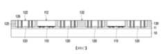
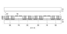
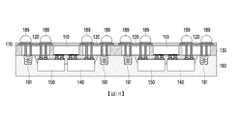
圖1A至圖1H是依照本發明的第一實施例的一種封裝結構的部分製造方法的部分剖視示意圖。圖1I是依照本發明的第一實施例的一種封裝結構的部分剖視示意圖。圖1J是依照本發明的第一實施例的一種封裝結構的部分下視示意圖。圖1K至圖1L是依照本發明的第一實施例的一種封裝結構的部分剖視放大示意圖。圖1I例如是對應於圖1J中A-A’剖線上的剖視示意圖。圖1K例如是對應於圖1I中區域R1的放大示意圖。圖1L例如是對應於圖1I中區域R2的放大示意圖。另外,為求清楚表示,於圖式中可能省略繪示了部分的膜層或構件。舉例而言,於圖1J中,僅示例性地繪示了部分的橋接晶片110、矽穿孔晶片120、第一主動晶片140、第二主動晶片150、第一導電連接件181、第二導電連接件182、第三導電連接件183、第四導電連接件184、導電端子189或被動元件191。1A to 1H are partial cross-sectional schematic views of a part of a method for manufacturing a package structure according to a first embodiment of the present invention. FIG. 1I is a partial cross-sectional schematic diagram of a package structure according to the first embodiment of the present invention. FIG. 1J is a partial bottom view of a package structure according to the first embodiment of the present invention. 1K to 1L are partial cross-sectional enlarged schematic views of a package structure according to the first embodiment of the present invention. Fig. 1I is, for example, a schematic cross-sectional view corresponding to the line A-A' in Fig. 1J. FIG. 1K is, for example, an enlarged schematic view corresponding to the region R1 in FIG. 1I . FIG. 1L is, for example, an enlarged schematic view corresponding to the region R2 in FIG. 1I . In addition, for the sake of clarity, some of the film layers or components may be omitted from the drawings. For example, in FIG. 1J , only part of the
請參照圖1A,提供矽穿孔晶片120及橋接晶片110。舉例而言,可以將矽穿孔晶片120及橋接晶片110配置於第一載板10上。第一載板10可以由玻璃、晶圓基板、金屬或其他適宜的材料所製成,只要前述的材料能夠於後續的製程中,承載形成於其上的結構或構件。另外,本發明對於配置於第一載板10上的矽穿孔晶片120或橋接晶片110的個數並不加以限制。以圖1A為例,配置於第一載板10上的矽穿孔晶片120的個數例如為四個,且配置於第一載板10上的橋接晶片110的個數例如為二個。Referring to FIG. 1A , a TSV
在本實施例中,第一載板10上可以具有離型層11。離型層11可以為光熱轉換(light to heat conversion,LTHC)黏著層,但本發明不限於此。In this embodiment, a
在本實施例中,矽穿孔晶片120可以包括矽基材125、穿矽導體126以及連接墊127。穿矽導體126可以貫穿矽基材125,且穿矽導體126可以電性連接於對應的連接墊127。連接墊127位於矽基材125上。矽穿孔晶片120可以是以其連接墊127面向第一載板10的方式而被配置於第一載板10上。藉由矽穿孔晶片120,可以使位於矽穿孔晶片120相對兩端的電子元件可以藉由矽穿孔晶片120的穿矽導體126而電性連接。In this embodiment, the TSV 120 may include a
在本實施例中,被配置於第一載板10上的矽穿孔晶片120可以為已知合格晶片(known good die,KGD)。舉例而言,在將矽穿孔晶片120配置於第一載板10上之前,可以對矽穿孔晶片120進行電性、外觀或其他適宜的檢查或測試步驟。如此一來,可以確認被配置於第一載板10上的矽穿孔晶片120具有良好的功能,而可以提升封裝結構100(標示於圖1I或圖1J)的良率。In this embodiment, the
在本實施例中,橋接晶片110可以包括矽基材115以及內連線結構116。內連線結構116位於矽基材115上。橋接晶片110可以是以其內連線結構116面向第一載板10的方式而被配置於第一載板10上。In this embodiment, the
在本實施例中,內連線結構116例如為藉由一般半導體製造中的後段製程線路(back-end of line,BEOL)製程所形成的線路。因此,可以依據後續電性連接的需求,將內連線結構116的線路進行調整或設計,以使橋接晶片110在應用上可以具有較多的彈性,且可以使線路或電性接點間具有較佳的細節距(fine pitch)。In this embodiment, the
在本實施例中,被配置於第一載板10上的橋接晶片110可以為已知合格晶片(known good die;KGD)。舉例而言,在將橋接晶片110配置於第一載板10上之前,可以對橋接晶片110進行電性、外觀或其他適宜的檢查或測試步驟。如此一來,可以確認被配置於第一載板10上的橋接晶片110具有良好的功能,而可以提升封裝結構100(標示於圖1I或圖1J)的良率。In this embodiment, the bridge die 110 disposed on the
在一實施例中,矽穿孔晶片120或橋接晶片110不具有主動元件(active device)。舉例來說,矽基材115上的膜層可以不會構成電晶體(transistor)、二極體(diode)、積體電路(integrated circuit)或光電元件(optoelectronic device)。如此一來,橋接晶片110在製作、檢查或測試上可以較為簡單。在一實施例中,矽穿孔晶片120或橋接晶片110可以為被動晶片(passive die)。In one embodiment,
請參照圖1B至圖1C,形成覆蓋矽穿孔晶片120及橋接晶片110的第一模封體130。Referring to FIG. 1B to FIG. 1C , a
請參照圖1B,舉例而言,可以形成覆蓋矽穿孔晶片120及橋接晶片110的第一模封材料139。在一實施例中,第一模封材料139例如是藉由模塑製程(molding process)或其他適宜的方法將熔融的模塑化合物(molding compound)形成於第一載板10上。然後,使熔融的模塑化合物冷卻並且固化。在一實施例中,矽穿孔晶片120及橋接晶片110並不會被暴露於第一模封材料139之外,但本發明不限於此。Referring to FIG. 1B , for example, a
請參照圖1C,舉例而言,在形成第一模封材料139之後,可以進行第一減薄製程,以移除部分的第一模封材料139,以形成側向覆蓋矽穿孔晶片120及橋接晶片110的第一模封體130,且暴露出矽穿孔晶片120及橋接晶片110。Referring to FIG. 1C , for example, after the
在本實施例中,第一減薄製程例如包括化學機械研磨(chemical mechanical polishing,CMP)、機械研磨(mechanical grinding)、蝕刻(etching)或其他適宜的製程,但本發明不限於此。In this embodiment, the first thinning process includes, for example, chemical mechanical polishing (CMP), mechanical grinding (mechanical grinding), etching (etching) or other suitable processes, but the invention is not limited thereto.
在本實施例中,在經由上述的第一減薄製程之後,矽穿孔晶片120的第二連接面122、橋接晶片110的橋接背面112及第一模封材料139的第二模封表面132可以基本上共面(coplaner)。In this embodiment, after the above-mentioned first thinning process, the
在一實施例中,在上述的第一減薄製程中,矽穿孔晶片120的一部份(如:矽基材125遠離第一載板10的一部分或穿矽導體126遠離第一載板10的一部分)或橋接晶片110的一部份(如:矽基材115遠離第一載板10的一部分)可能可以被些微地移除。In one embodiment, in the above-mentioned first thinning process, a part of the TSV 120 (eg, a part of the
請參照圖1D,形成電性連接於矽穿孔晶片120的重佈線路結構170。舉例而言,於形成第一模封體130之後,可以至少於矽穿孔晶片120上形成重佈線路結構170,且重佈線路結構170可以電性連接於矽穿孔晶片120的穿矽導體126。Referring to FIG. 1D , a redistributed
在本實施例中,重佈線路結構170可以被形成於矽穿孔晶片120、橋接晶片110以及第一模封體130上。舉例而言,可以於矽穿孔晶片120、橋接晶片110以及第一模封體130上形成圖案化介電層175。圖案化介電層175可以具有多個介電層開口,以暴露出部分的穿矽導體126。然後,可以藉由沉積製程及/或電鍍製程等其他適宜的製程在圖案化介電層175上形成導電物質。並且,導電物質可以進一步填入圖案化介電層175的介電層開口內,以形成具有導電性質的導通孔(conductive via)。隨後,可以藉由例如微影及蝕刻製程以對覆蓋於圖案化介電層175上的導電物質進行圖案化,以形成圖案化導電層176。藉由相同或相似於上述的步驟,可以形成至少一個圖案化介電層175或至少一個圖案化導電層176,以構成重佈線路結構170。In this embodiment, the redistributed
請參照圖1E至圖1F,將矽穿孔晶片120、橋接晶片110、第一模封體130及重佈線路結構170放置於第二載板20上,且移除第一載板10。Referring to FIGS. 1E to 1F , the
在一實施例中,可以先將在第一載板10及位於第一載板10上的構件(如:圖1D所繪示的結構)上配置第二載板20,以使第一載板10上的構件(如:矽穿孔晶片120、橋接晶片110、第一模封體130及重佈線路結構170)被夾於第二載板20與第一載板10之間。然後,可以將第一載板10、第二載板20以及被夾於第二載板20與第一載板10之間的構件上下翻轉(flip upside down)。然後,再將第一載板10移除。值得注意的是,上述的方式僅為示例性的舉例,於本發明並不加以限制。In one embodiment, the
在本實施例中,第二載板20上可以具有離型層21。離型層21可以為光熱轉換黏著層,但本發明不限於此。In this embodiment, a
在本實施例中,在移除第一載板10之後,矽穿孔晶片120的連接墊127及橋接晶片110的內連線結構116可以被暴露出。In this embodiment, after the
請參照圖1F,在移除第一載板10之後,配置第一主動晶片140或第二主動晶片150。第一主動晶片140或第二主動晶片150電性連接於橋接晶片110,且第一主動晶片140電性連接於矽穿孔晶片120。值得注意的是,本發明對於第一主動晶片140或第二主動晶片150配置的數量或順序並不加以限制。Referring to FIG. 1F , after the
在本實施例中,在經由前述的第一減薄製程之後,橋接晶片110及矽穿孔晶片120的厚度基本上相同。並且,橋接晶片110及矽穿孔晶片120可以包括硬質的基材(如:橋接晶片110包括矽基材115,且矽穿孔晶片120包括矽基材125)。另外,橋接晶片110及矽穿孔晶片120被第一模封體130至少側向覆蓋且固定。如此一來,在將第一主動晶片140或第二主動晶片150配置於橋接晶片110或矽穿孔晶片120上時,可以降低側向的位移(shift)或提升垂直方向的接合力,而可以提升封裝結構100的製造良率或品質。在一實施例中,第一模封體130可以完全覆蓋橋接晶片110的橋接側面113及矽穿孔晶片120的連接側面123。In this embodiment, after the aforementioned first thinning process, the thicknesses of the
在一實施例中,第一主動晶片140或第二主動晶片150可以是電力管理晶片(power management integrated circuit,PMIC)、微機電系統晶片(micro-electro-mechanical-system,MEMS)、特殊應用積體電路晶片(Application-specific integrated circuit,ASIC)、動態隨機存取記憶體晶片(dynamic random access memory,DRAM)、靜態隨機存取記憶體晶片(static random access memory,SRAM)、高頻寬記憶體(High Bandwidth Memory,HBM)晶片、系統晶片(system on chip,SoC)或其他類似的高效能運算(High Performance Computing,HPC)晶片,但本發明不限於此。In one embodiment, the first
在一實施例中,第一主動晶片140與第二主動晶片150之間可以是同質的(homogeneous)晶片也可以是異質的(heterogeneous)晶片,於本發明並不加以限制。In one embodiment, the first
在本實施例中,更可以在移除第一載板10之後,配置被動元件191。被動元件191可以電性連接於矽穿孔晶片120。值得注意的是,本發明對於第一主動晶片140、第二主動晶片150或被動元件191配置的數量或順序並不加以限制。在一實施例中,被動元件191例如是積層陶瓷電容器(Multi-layer Ceramic Capacitor,MLCC),但本發明不限於此。In this embodiment, the
請參照圖1G,形成覆蓋第一主動晶片140及第二主動晶片150的第二模封體160。第二模封體160的材質或形成方式相同或相似於第一模封體130,故於此不加以贅述。Referring to FIG. 1G , a
在本實施例中,第一主動晶片140及第二主動晶片150並不會被暴露於第二模封體160之外,但本發明不限於此。In this embodiment, the first
在本實施例中,第二模封體160可以更覆蓋被動元件191,且被動元件191並不會被暴露於第二模封體160之外,但本發明不限於此。In this embodiment, the
請參照圖1G至圖1H,於形成第二模封體160之後,可以移除第二載板20。並且,可以在移除第二載板20之後,形成多個導電端子189。導電端子189可以電性連接於重佈線路結構170。Referring to FIGS. 1G to 1H , after the
導電端子189可以是導電柱(conductive pillar)、焊球(solder ball)、導電凸塊(conductive bump)或具有其他形式或形狀的導電端子189。導電端子189可以經由電鍍、沉積、置球(ball placement)、迴焊(reflow)及/或其他適宜的製程來形成。The
請參照圖1H至圖1I,在本實施例中,可以經由單一化製程(singulation process),以構成多個封裝結構100。單一化製程例如可以包括切割製程(dicing process/cutting process),以切穿第一模封體130、第二模封體160及/或重佈線路結構170。Referring to FIG. 1H to FIG. 1I , in this embodiment, a plurality of
值得注意的是,在進行單一化製程之後,相似的元件符號將用於單一化後的元件。舉例而言,橋接晶片110(如圖1H所示)於單一化後可以為橋接晶片110(如圖1I所示),矽穿孔晶片120(如圖1H所示)於單一化後可以為矽穿孔晶片120(如圖1I所示),第一模封體130(如圖1H所示)於單一化後可以為第一模封體130(如圖1I所示),第一主動晶片140(如圖1H所示)於單一化後可以為第一主動晶片140(如圖1I所示),第二主動晶片150(如圖1H所示)於單一化後可以為第二主動晶片150(如圖1I所示),第二模封體160(如圖1H所示)於單一化後可以為第二模封體160(如圖1I所示),重佈線路結構170(如圖1H所示)於單一化後可以為重佈線路結構170(如圖1I所示),諸如此類。其他單一化後的元件將依循上述相同的元件符號規則,於此不加以贅述或特別繪示。It is worth noting that after the singulation process, similar reference numerals will be used for the singulated components. For example, the bridge chip 110 (shown in FIG. 1H ) can be the bridge chip 110 (shown in FIG. 1I ) after singulation, and the TSV chip 120 (shown in FIG. 1H ) can be TSV after singulation The chip 120 (shown in FIG. 1I ), the first mold body 130 (shown in FIG. 1H ) can be the first mold body 130 (shown in FIG. 1H ) can be the first active chip 140 (shown in FIG. 1I ) after singulation, and the second active chip 150 (shown in FIG. 1H ) can be the second
值得注意的是,本發明並未限定配置多個導電端子189(若有)以及單一化製程(若有)的順序。It should be noted that the present invention does not limit the order of disposing the plurality of conductive terminals 189 (if any) and the singulation process (if any).
經過上述步驟後即可大致上完成本實施例的封裝結構100的製作。After the above steps, the fabrication of the
請參照圖1I至圖1L,封裝結構100包括橋接晶片110、矽穿孔晶片120、第一模封體130、第一主動晶片140、第二主動晶片150、第二模封體160以及重佈線路結構170。第一模封體130覆蓋多個矽穿孔晶片120及橋接晶片110。第一主動晶片140電性連接於橋接晶片110及矽穿孔晶片120。第二主動晶片150電性連接於橋接晶片110。第二模封體160覆蓋第一主動晶片140及第二主動晶片150。重佈線路結構170電性連接於矽穿孔晶片120,其中矽穿孔晶片120位於第一主動晶片140及重佈線路結構170之間。Referring to FIGS. 1I to 1L, the
在本實施例中,第一模封體130的側壁、第二模封體160的側壁及重佈線路結構170的側壁基本上可以相切齊。In this embodiment, the sidewalls of the first molded
在本實施例中,橋接晶片110具有橋接連接面111、橋接背面112以及橋接側面113。橋接背面112相對於橋接連接面111。橋接側面113連接於橋接連接面111及橋接背面112。橋接晶片110包括矽基材115以及內連線結構116。內連線結構116位於矽基材115上。In this embodiment, the
在本實施例中,內連線結構116例如為多層的內連線結構。舉例而言,內連線結構116包括多個導電層116a以及多個絕緣層116b,且部分的導電層116a1與部分的導電層116a2可以交錯(interlace/ intercross)。如此一來,可以提升內連線結構116在佈線空間利用率(layout utilization),而可以藉由橋接晶片110的內連線結構116連接多個晶片或多個晶片的多個接點。In this embodiment, the
在一實施例中,內連線結構116遠離矽基材115的部分表面(如:內連線結構116最遠離矽基材115的表面)可以構成橋接連接面111,但本發明不限於此。In one embodiment, a part of the surface of the
在一實施例中,矽基材115遠離內連線結構116的部分表面(如:矽基材115最遠離內連線結構116的表面)可以構成橋接背面112,但本發明不限於此。In one embodiment, a part of the surface of the
在本實施例中,矽穿孔晶片120具有第一連接面121、第二連接面122以及連接側面123。第二連接面122相對於第一連接面121。連接側面123連接於第一連接面121及第二連接面122。矽穿孔晶片120可以包括矽基材125、穿矽導體126以及連接墊127。穿矽導體126貫穿矽基材125。連接墊127位於矽基材125上。In this embodiment, the
在本實施例中,穿矽導體126包括導電芯層126a及側向包覆導電芯層126a的絕緣殼層126b。矽基材125的部分表面(如:矽基材125最遠離連接墊127的表面)、導電芯層126a的部分表面以及絕緣殼層126b的部分表面基本上共面(coplaner)且構成第二連接面122。In this embodiment, the through-
在一實施例中,矽基材125的部分表面(如:矽基材125具有連接墊127於其上的部分表面)或連接墊127的部分表面可以構成第一連接面121,但本發明不限於此。In one embodiment, a part of the surface of the silicon substrate 125 (eg, a part of the surface of the
在本實施例中,連接墊127可以包括導電連接層127a。導電芯層126a與導電連接層127a可以為相同的膜層。In this embodiment, the
在本實施例中,第一主動晶片140具有第一主動面141、第一背面142以及第一側面143。第一背面142相對於第一主動面141。第一側面143連接於第一主動面141及第一背面142。第一主動晶片140的第一主動面141面向矽穿孔晶片120的第一連接面121,且第一主動面141與第一連接面121部分重疊。第一主動晶片140的第一主動面141面向橋接晶片110的橋接連接面111,且第一主動面141與橋接連接面111部分重疊。In this embodiment, the first
在本實施例中,第一主動晶片140的第一主動面141與矽穿孔晶片120的第一連接面121之間可以具有第一導電連接件181。第一主動晶片140與矽穿孔晶片120可以藉由第一導電連接件181而彼此電性連接。In this embodiment, there may be a first
在本實施例中,第一主動晶片140的第一主動面141與橋接晶片110的橋接連接面111之間可以具有第二導電連接件182。第一主動晶片140與橋接晶片110可以藉由第二導電連接件182而彼此電性連接。In this embodiment, there may be a second
在本實施例中,第二主動晶片150具有第二主動面151、第二背面152以及第二側面153。第二背面152相對於第二主動面151。第二側面153連接於第二主動面151及第二背面152。第二主動晶片150的第二主動面151面向橋接晶片110的橋接連接面111,且第二主動面151與橋接連接面111部分重疊。In this embodiment, the second
在本實施例中,第二主動晶片150的第二主動面151與橋接晶片110的橋接連接面111之間可以具有第三導電連接件183。第二主動晶片150與橋接晶片110可以藉由第三導電連接件183而彼此電性連接。In this embodiment, there may be a third
在本實施例中,第二主動晶片150可以電性連接於另一矽穿孔晶片120,但本發明不限於此。舉例而言,第二主動晶片150的第二主動面151與另一矽穿孔晶片120的第一連接面121之間可以具有第四導電連接件184。第二主動晶片150與另一矽穿孔晶片120的矽穿孔晶片120可以藉由第四導電連接件184而彼此電性連接。In this embodiment, the second
在一實施例中,第一導電連接件181、第二導電連接件182、第三導電連接件183或第四導電連接件184可以是焊球(solder ball)或具有其他形式或形狀的導電連接件,於本發明並不加以限制。In one embodiment, the first
在本實施例中,第一模封體130可以覆蓋矽穿孔晶片120的連接側面123以及橋接晶片110的橋接側面113。第一模封體130具有第一模封表面131及第二模封表面132。第二模封表面132相對於第一模封表面131。In this embodiment, the
在本實施例中,矽穿孔晶片120的第二連接面122、橋接晶片110的橋接背面112及第一模封體130的第二模封表面132基本上共面(coplaner)。In the present embodiment, the
在一實施例中,第一模封體130可以是均質材料(homogeneous material),且前述的均質材料無法再藉由機械方法(如:破碎、剪、切、鋸、磨等方式)將元件拆離成不同的單一材料。換句話說,在第一模封體130內可以不具有因不同材質或不同製程所形成的介面(interface)。In one embodiment, the first molded
在本實施例中,第二模封體160可以覆蓋第一主動晶片140的第一側面143或第一背面142,且第二模封體160可以覆蓋第二主動晶片150的第二側面153或第二背面152。In this embodiment, the
在一實施例中,第二模封體160可以是均質材料。換句話說,在第二模封體160內可以不具有因不同材質或不同製程所形成的介面。In one embodiment, the
在本實施例中,第一模封體130的第一模封表面131面向第二模封體160,且第一模封體130的第一模封表面131與第二模封體160物理性地接觸(physically contact)。In this embodiment, the
在一實施例中,由於第一模封體130與第二模封體160是在不同的步驟中所形成的,因此,第一模封體130與第二模封體160之間可能具有一界面S1。In one embodiment, since the first molded
在本實施例中,重佈線路結構170至少位於矽穿孔晶片120的第二連接面122上。舉例而言,重佈線路結構170可以位於矽穿孔晶片120的第二連接面122、橋接晶片110的橋接背面112以及第一模封體130的第二模封表面132上。重佈線路結構170可以包括圖案化介電層175以及圖案化導電層176,且部分的圖案化介電層175可以貫穿圖案化導電層176。In this embodiment, the redistributed
在本實施例中,最接近矽穿孔晶片120的圖案化導電層176a(即,多個圖案化導電層176的其中之一)可以與矽穿孔晶片120的穿矽導體126的導電芯層126a相接觸。在一實施例中,由於前述的圖案化導電層176a與導電芯層126a是在不同的步驟中所形成的,因此,前述的圖案化導電層176與導電芯層126a之間可以具有一界面S2。In the present embodiment, the patterned conductive layer 176 a closest to the TSV 120 (ie, one of the plurality of patterned conductive layers 176 ) may be in phase with the
在本實施例中,封裝結構100可以更包括被動元件191,且第二模封體160可以更覆蓋被動元件191。被動元件191可以電性連接於矽穿孔晶片120中對應的穿矽導體126。舉例而言,矽穿孔晶片120的穿矽導體126可以包括多個第一穿矽導體126’以及多個第二穿矽導體126”。第一穿矽導體126’可以重疊且電性連接於第一主動晶片140或第二主動晶片150。第二穿矽導體126”可以重疊且電性連接於被動元件191。In this embodiment, the
在本實施例中,多個第一穿矽導體126’之間具有第一間距P1,多個第二穿矽導體126”之間具有第二間距P2,且第二間距P2大於或等於第一間距P1。In this embodiment, the plurality of first through-silicon conductors 126' have a first pitch P1, and the plurality of second through-
在本實施例中,封裝結構100可以更包括填充層193。填充層193可以位於第一主動晶片140與矽穿孔晶片120、第一主動晶片140與橋接晶片110之間以及第二主動晶片150與橋接晶片110之間。填充層193例如是毛細填充膠(Capillary Underfill,CUF)或其他適宜的填充材料,於本發明並不加以限制。In this embodiment, the
在本實施例中,封裝結構100可以藉由橋接晶片110的內連線結構116以將至少兩個主動晶片(如:第一主動晶片140或第二主動晶片150)電性連接。並且,內連線結構116藉可以藉由一般半導體製造中的後段製程線路製程所形成。因此,相較於一般常用的電路板,可以使橋接晶片110的內連線結構116內的線路或電性接點間的節距(pitch)可以與其所連接的主動晶片(如:第一主動晶片140或第二主動晶片150)相對應,且可以使橋接晶片110的內連線結構116內的線路或電性接點具有較佳的細節距(fine pitch)。In this embodiment, the
在本實施例中,封裝結構100的主動晶片(如:第一主動晶片140或第二主動晶片150)可以藉由矽穿孔晶片120以與外界的電子元件電性連接。並且,由於矽穿孔晶片120內的穿矽導體126基本上為垂直的導通路徑。因此,藉由矽穿孔晶片120內的穿矽導體126可以降低電子訊號傳遞的路徑或時間,而可以提升電子訊號的傳輸品質。In this embodiment, the active chip (eg, the first
一般而言,主動晶片(如:第一主動晶片140或第二主動晶片150)的價值或價格高於不具有主動元件的晶片(如:橋接晶片110或矽穿孔晶片120)。因此,在本實施例中,封裝結構100的製造方法是先將已知合格的橋接晶片110及已知合格的矽穿孔晶片120以第一模封體130包覆後,再配置電性連接至橋接晶片110或矽穿孔晶片120的主動晶片(如:第一主動晶片140或第二主動晶片150)。如此一來,可以使封裝結構100的製造良率提升,或可以使封裝結構100的製造成本降低。Generally speaking, the value or price of an active chip (eg, the first
圖2A是依照本發明的第二實施例的一種封裝結構的部分剖視示意圖。圖2B是依照本發明的第二實施例的一種封裝結構的部分下視示意圖。圖2A例如是對應於圖2B中B-B’剖線上的剖視示意圖。2A is a partial cross-sectional schematic diagram of a package structure according to a second embodiment of the present invention. 2B is a partial bottom view of a package structure according to the second embodiment of the present invention. Fig. 2A is, for example, a schematic cross-sectional view corresponding to the line B-B' in Fig. 2B.
在本實施例中,封裝結構200的製造方法與封裝結構100的製造方法相似,其類似的構件以相同的標號表示,且具有類似的功能、材質或形成方式,並省略描述。In this embodiment, the manufacturing method of the
請參照圖2A及圖2B,在本實施例中,封裝結構200包括多個橋接晶片110、多個矽穿孔晶片120、第一模封體130、多個第一主動晶片140、第二主動晶片150、第二模封體160以及重佈線路結構170。Referring to FIGS. 2A and 2B , in this embodiment, the
在本實施例中,第一主動晶片140與第二主動晶片150之間可以是異質的晶片,且多個第一主動晶片140之間可以是同質的晶片。舉例而言,第一主動晶片140可以是高頻寬記憶體晶片,而第二主動晶片150可以是系統晶片。In this embodiment, the first
圖3是依照本發明的第三實施例的一種封裝結構的部分剖視示意圖。3 is a partial cross-sectional schematic diagram of a package structure according to a third embodiment of the present invention.
在本實施例中,封裝結構300的製造方法與封裝結構100的製造方法相似,其類似的構件以相同的標號表示,且具有類似的功能、材質或形成方式,並省略描述。In the present embodiment, the manufacturing method of the
在本實施例中,封裝結構300包括橋接晶片110、矽穿孔晶片320、第一模封體130、第一主動晶片140、第二主動晶片150、第二模封體160以及重佈線路結構170。第二模封體160覆蓋第一主動晶片140及第二主動晶片150。第一模封體130覆蓋多個矽穿孔晶片320及橋接晶片110。第一主動晶片140電性連接於橋接晶片110及矽穿孔晶片320。重佈線路結構170電性連接於矽穿孔晶片320,其中矽穿孔晶片320位於第一主動晶片140及重佈線路結構170之間。In the present embodiment, the
在本實施例中,矽穿孔晶片320可以包括矽基材125、穿矽導體126、連接墊127以及連接線路328。連接線路328位於矽基材125上。In this embodiment, the
在本實施例中,連接墊127與連接線路328可以藉由相同或相似的步驟所形成。也就是說,連接墊127的結構、材質或厚度可以相同或相似於連接線路328的結構、材質或厚度。舉例而言,連接墊127的結構、材質或厚度基本上相同於連接線路328的結構、材質或厚度。In this embodiment, the
在本實施例中,連接線路328可以與穿矽導體126物理性地絕緣(physically isolated),但本發明不限於此。In this embodiment, the
在本實施例中,封裝結構300可以更包括被動元件191。被動元件191可以藉由連接線路328電性連接第一主動晶片140或第二主動晶片150。In this embodiment, the
圖4是依照本發明的第四實施例的一種封裝結構的部分剖視示意圖。4 is a partial cross-sectional schematic diagram of a package structure according to a fourth embodiment of the present invention.
在本實施例中,封裝結構400的製造方法與封裝結構100的製造方法相似,其類似的構件以相同的標號表示,且具有類似的功能、材質或形成方式,並省略描述。In this embodiment, the manufacturing method of the
在本實施例中,封裝結構400包括橋接晶片110、矽穿孔晶片120、第一模封體130、第一主動晶片140、第二主動晶片150、第二模封體460以及重佈線路結構170。第二模封體460覆蓋第一主動晶片140及第二主動晶片150。In the present embodiment, the
在本實施例中,第二模封體460可以覆蓋第一主動晶片140的第一側面143及第二主動晶片150的第二側面153,且第二模封體460可以暴露出第一主動晶片140的第一背面142及第二主動晶片150的第二背面152。In this embodiment, the
在本實施例中,封裝結構400可以更包括散熱件493。散熱件493至少熱耦接於第一主動晶片140或第二主動晶片150。In this embodiment, the
舉例而言,請參照圖1G及圖4,於配置第一主動晶片140及第二主動晶片150之後,可以形成覆蓋第一主動晶片140及第二主動晶片150的第二模封材料(如:類似於圖1G所繪示的步驟)。第二模封材料的材質或形成方式相同或相似於第一模封材料139(標示於圖1B),故於此不加以贅述。然後,在形成前述的第二模封材料之後,可以進行第二減薄製程,以形成側向覆蓋第一主動晶片140及第二主動晶片150的第二模封體460,且暴露出第一主動晶片140及第二主動晶片150。第二減薄製程相同或相似於前述的第一減薄製程,故於此不加以贅述。For example, referring to FIG. 1G and FIG. 4 , after the first
在本實施例中,散熱件493可以接觸第一主動晶片140的第一背面142及第二主動晶片150的第二背面152,以使散熱件493可以熱耦接於第一主動晶片140或第二主動晶片150。In this embodiment, the
在一未繪示實施例中,散熱件493與第一主動晶片140的第一背面142或第二主動晶片150的第二背面152之間可以具有熱界面材料(Thermal Interface Material,TIM),以使散熱件493可以熱耦接於第一主動晶片140或第二主動晶片150。In a not-shown embodiment, a thermal interface material (TIM) may be provided between the
綜上所述,本發明的封裝結構可以整合多個主動晶片。多個主動晶片之間可以藉由橋接晶片彼此電性連接,且主動晶片可以藉由矽穿孔晶片與重佈線路結構電性連接。如此一來,可以提升封裝結構的品質。並且,在封裝結構的製造方法上,可以先將橋接晶片與矽穿孔晶片以第一模封體,再配置電性連接至橋接晶片或矽穿孔晶片的主動晶片。如此一來,封裝結構的製造良率可以提升,或可以使封裝結構的製造成本降低。To sum up, the package structure of the present invention can integrate multiple active chips. A plurality of active chips can be electrically connected to each other through bridge chips, and the active chips can be electrically connected to the redistributed circuit structure through TSV chips. In this way, the quality of the package structure can be improved. In addition, in the manufacturing method of the package structure, the bridge chip and the TSV chip can be firstly formed into a first molding body, and then the active chip electrically connected to the bridge chip or the TSV chip can be arranged. In this way, the manufacturing yield of the package structure can be improved, or the manufacturing cost of the package structure can be reduced.
100、200、300、400:封裝結構110:橋接晶片111:橋接連接面112:橋接背面113:橋接側面115:矽基材116:內連線結構116a:導電層116b:絕緣層120、320:矽穿孔晶片121:第一連接面122:第二連接面123:連接側面125:矽基材126:穿矽導體126a:導電芯層126b:絕緣殼層126’:第一穿矽導體126”:第二穿矽導體127:連接墊127a:導電連接層328:連接線路139:第一模封材料130:第一模封體131:第一模封表面132:第二模封表面140:第一主動晶片141:第一主動面142:第一背面143:第一側面150:第二主動晶片151:第二主動面152:第二背面153:第二側面160、460:第二模封體170:重佈線路結構175:圖案化介電層176、176a:圖案化導電層181:第一導電連接件182:第二導電連接件183:第三導電連接件184:第四導電連接件189:導電端子191:被動元件193:填充層S1、S2:界面493:散熱件10:第一載板20:第二載板11、21:離型層P1:第一間距P2:第一間距R1、R2:區域100, 200, 300, 400: Package structure110: Bridge chip111: Bridge connection surface112: Bridge back113: Bridge Side115: Silicon substrate116: Interconnect structure116a: Conductive layer116b: insulating layer120, 320: TSV121: The first connection surface122: Second connection surface123: Connect the side125: Silicon substrate126: Through silicon conductor126a: Conductive core layer126b: insulating shell126': first through-silicon conductor126": 2nd through-silicon conductor127: Connection pad127a: Conductive connection layer328: Connection Line139: First molding material130: The first molded body131: First molding surface132: Second molding surface140: The first active chip141: The first active side142: The first back143: The first side150: The second active chip151: Second Active Side152: Second back153: Second side160, 460: The second molded body170: Redistribute the wiring structure175: Patterned Dielectric Layer176, 176a: Patterned conductive layer181: The first conductive connector182: Second conductive connector183: Third conductive connector184: Fourth conductive connector189: Conductive terminal191: Passive Components193: Filler LayerS1, S2: interface493: heat sink10: The first carrier board20: Second carrier board11, 21: release layerP1: first pitchP2: first pitchR1, R2: area
圖1A至圖1H是依照本發明的第一實施例的一種封裝結構的部分製造方法的部分剖視示意圖。圖1I是依照本發明的第一實施例的一種封裝結構的部分剖視示意圖。圖1J是依照本發明的第一實施例的一種封裝結構的部分下視示意圖。圖1K至圖1L是依照本發明的第一實施例的一種封裝結構的部分剖視放大示意圖。圖2A是依照本發明的第二實施例的一種封裝結構的部分剖視示意圖。圖2B是依照本發明的第二實施例的一種封裝結構的部分下視示意圖。圖3是依照本發明的第三實施例的一種封裝結構的部分剖視示意圖。圖4是依照本發明的第四實施例的一種封裝結構的部分剖視示意圖。1A to 1H are partial cross-sectional schematic views of a part of a method for manufacturing a package structure according to a first embodiment of the present invention.FIG. 1I is a partial cross-sectional schematic diagram of a package structure according to the first embodiment of the present invention.FIG. 1J is a partial bottom view of a package structure according to the first embodiment of the present invention.1K to 1L are partial cross-sectional enlarged schematic views of a package structure according to the first embodiment of the present invention.2A is a partial cross-sectional schematic diagram of a package structure according to a second embodiment of the present invention.2B is a partial bottom view of a package structure according to the second embodiment of the present invention.3 is a partial cross-sectional schematic diagram of a package structure according to a third embodiment of the present invention.4 is a partial cross-sectional schematic diagram of a package structure according to a fourth embodiment of the present invention.
100:封裝結構100: Package structure
110:橋接晶片110: Bridge chip
111:橋接連接面111: Bridge connection surface
112:橋接背面112: Bridge back
113:橋接側面113: Bridge Side
115:矽基材115: Silicon substrate
116:內連線結構116: Interconnect structure
120:矽穿孔晶片120: TSV
121:第一連接面121: The first connection surface
122:第二連接面122: Second connection surface
123:連接側面123: Connect the side
125:矽基材125: Silicon substrate
126:穿矽導體126: Through silicon conductor
126’:第一穿矽導體126': first through-silicon conductor
126”:第二穿矽導體126": 2nd through-silicon conductor
127:連接墊127: Connection pad
130:第一模封體130: The first molded body
131:第一模封表面131: First molding surface
132:第二模封表面132: Second molding surface
140:第一主動晶片140: The first active chip
141:第一主動面141: The first active side
142:第一背面142: The first back
143:第一側面143: The first side
150:第二主動晶片150: The second active chip
151:第二主動面151: Second Active Side
152:第二背面152: Second back
153:第二側面153: Second side
160:第二模封體160: Second molded body
170:重佈線路結構170: Redistribute the wiring structure
181:第一導電連接件181: The first conductive connector
182:第二導電連接件182: Second conductive connector
183:第三導電連接件183: Third conductive connector
184:第四導電連接件184: Fourth conductive connector
189:導電端子189: Conductive terminal
191:被動元件191: Passive Components
193:填充層193: Filler Layer
S1:界面S1: Interface
P1:第一間距P1: first pitch
P2:第一間距P2: first pitch
R1、R2:區域R1, R2: area
Claims (9)
Translated fromChinesePriority Applications (1)
| Application Number | Priority Date | Filing Date | Title |
|---|---|---|---|
| US17/099,801US11309283B2 (en) | 2019-12-31 | 2020-11-17 | Packaging structure and manufacturing method thereof |
Applications Claiming Priority (2)
| Application Number | Priority Date | Filing Date | Title |
|---|---|---|---|
| US201962955456P | 2019-12-31 | 2019-12-31 | |
| US62/955,456 | 2019-12-31 |
Publications (2)
| Publication Number | Publication Date |
|---|---|
| TW202127595A TW202127595A (en) | 2021-07-16 |
| TWI768294Btrue TWI768294B (en) | 2022-06-21 |
Family
ID=75237134
Family Applications (8)
| Application Number | Title | Priority Date | Filing Date |
|---|---|---|---|
| TW109106328ATWI768294B (en) | 2019-12-31 | 2020-02-26 | Package structure and manufacturing method thereof |
| TW109111127ATWI721848B (en) | 2019-12-31 | 2020-04-01 | Package structure and manufacturing method thereof |
| TW109112111ATWI717255B (en) | 2019-12-31 | 2020-04-10 | Package structure and manufacturing method thereof |
| TW109119787ATWI764172B (en) | 2019-12-31 | 2020-06-12 | Package structure and manufacturing method thereof |
| TW109126211ATWI733542B (en) | 2019-12-31 | 2020-08-03 | Package structure and manufacturing method thereof |
| TW109126169ATWI725901B (en) | 2019-12-31 | 2020-08-03 | Package device and manufacturing method thereof |
| TW109126333ATWI725902B (en) | 2019-12-31 | 2020-08-04 | Semiconductor package structure and manufacturing method thereof |
| TW109135315ATWI728924B (en) | 2019-12-31 | 2020-10-13 | Package structure and manufacturing method thereof |
Family Applications After (7)
| Application Number | Title | Priority Date | Filing Date |
|---|---|---|---|
| TW109111127ATWI721848B (en) | 2019-12-31 | 2020-04-01 | Package structure and manufacturing method thereof |
| TW109112111ATWI717255B (en) | 2019-12-31 | 2020-04-10 | Package structure and manufacturing method thereof |
| TW109119787ATWI764172B (en) | 2019-12-31 | 2020-06-12 | Package structure and manufacturing method thereof |
| TW109126211ATWI733542B (en) | 2019-12-31 | 2020-08-03 | Package structure and manufacturing method thereof |
| TW109126169ATWI725901B (en) | 2019-12-31 | 2020-08-03 | Package device and manufacturing method thereof |
| TW109126333ATWI725902B (en) | 2019-12-31 | 2020-08-04 | Semiconductor package structure and manufacturing method thereof |
| TW109135315ATWI728924B (en) | 2019-12-31 | 2020-10-13 | Package structure and manufacturing method thereof |
Country Status (3)
| Country | Link |
|---|---|
| US (5) | US11557533B2 (en) |
| CN (8) | CN113130464B (en) |
| TW (8) | TWI768294B (en) |
Families Citing this family (17)
| Publication number | Priority date | Publication date | Assignee | Title |
|---|---|---|---|---|
| TWI768294B (en)* | 2019-12-31 | 2022-06-21 | 力成科技股份有限公司 | Package structure and manufacturing method thereof |
| US11614592B2 (en)* | 2020-01-22 | 2023-03-28 | Taiwan Semiconductor Manufacturing Co., Ltd. | Semiconductor devices and methods of manufacture |
| US12125820B2 (en)* | 2021-02-12 | 2024-10-22 | Taiwan Semiconductor Manufacturing Co., Ltd. | Through-dielectric vias for direct connection and method forming same |
| US12100697B2 (en)* | 2021-02-25 | 2024-09-24 | Advanced Semiconductor Engineering, Inc. | Semiconductor package structure |
| US11784157B2 (en) | 2021-06-04 | 2023-10-10 | Qualcomm Incorporated | Package comprising integrated devices coupled through a metallization layer |
| CN115706015A (en)* | 2021-08-11 | 2023-02-17 | 群创光电股份有限公司 | Method of manufacturing an electronic device |
| US11935871B2 (en) | 2021-08-30 | 2024-03-19 | Taiwan Semiconductor Manufacturing Company, Ltd. | Semiconductor package and method of fabricating the same |
| US12015003B2 (en) | 2021-09-29 | 2024-06-18 | International Business Machines Corporation | High density interconnection and wiring layers, package structures, and integration methods |
| TWI839645B (en)* | 2021-10-13 | 2024-04-21 | 矽品精密工業股份有限公司 | Electronic package and manufacturing method thereof |
| CN115995452A (en)* | 2021-10-18 | 2023-04-21 | 创意电子股份有限公司 | Interposer and Semiconductor Packaging |
| US20230187377A1 (en)* | 2021-12-14 | 2023-06-15 | Mediatek Inc. | Semiconductor package with integrated antenna and shielding pillars |
| TWI829063B (en)* | 2021-12-30 | 2024-01-11 | 漢民測試系統股份有限公司 | Testing substrate and manufacturing method thereof and probe card |
| US20240006270A1 (en)* | 2022-07-01 | 2024-01-04 | Taiwan Semiconductor Manufacturing Co., Ltd. | Package with Improved Heat Dissipation Efficiency and Method for Forming the Same |
| CN115132593B (en)* | 2022-09-02 | 2022-11-15 | 盛合晶微半导体(江阴)有限公司 | A three-dimensional packaging structure and its preparation method |
| US20240105626A1 (en)* | 2022-09-23 | 2024-03-28 | Apple Inc. | Semiconductor Package with Local Interconnect and Chiplet Integration |
| TWI840996B (en)* | 2022-10-13 | 2024-05-01 | 群創光電股份有限公司 | Electronic device and manufacturing method thereof |
| TWI842475B (en)* | 2023-04-13 | 2024-05-11 | 力成科技股份有限公司 | Package structure and manufacturing method thereof |
Citations (3)
| Publication number | Priority date | Publication date | Assignee | Title |
|---|---|---|---|---|
| WO2016036667A1 (en)* | 2014-09-05 | 2016-03-10 | Invensas Corporation | Multichip modules and methods of fabrication |
| US20180061741A1 (en)* | 2016-08-25 | 2018-03-01 | Imec Vzw | Semiconductor die package and method of producing the package |
| US20190103386A1 (en)* | 2017-09-29 | 2019-04-04 | Advanced Semiconductor Engineering, Inc. | Stacked semiconductor package assemblies including double sided redistribution layers |
Family Cites Families (78)
| Publication number | Priority date | Publication date | Assignee | Title |
|---|---|---|---|---|
| US6385049B1 (en)* | 2001-07-05 | 2002-05-07 | Walsin Advanced Electronics Ltd | Multi-board BGA package |
| US6965170B2 (en)* | 2003-11-18 | 2005-11-15 | International Business Machines Corporation | High wireability microvia substrate |
| JP2006165106A (en)* | 2004-12-03 | 2006-06-22 | Fuji Photo Film Co Ltd | Electronic component mounting method |
| JP4581768B2 (en)* | 2005-03-16 | 2010-11-17 | ソニー株式会社 | Manufacturing method of semiconductor device |
| JP4950743B2 (en)* | 2007-04-17 | 2012-06-13 | 株式会社フジクラ | Multilayer wiring board and manufacturing method thereof |
| JP5543058B2 (en)* | 2007-08-06 | 2014-07-09 | ピーエスフォー ルクスコ エスエイアールエル | Manufacturing method of semiconductor device |
| JP2011061004A (en)* | 2009-09-10 | 2011-03-24 | Elpida Memory Inc | Semiconductor device, and method of manufacturing the same |
| US9875911B2 (en)* | 2009-09-23 | 2018-01-23 | STATS ChipPAC Pte. Ltd. | Semiconductor device and method of forming interposer with opening to contain semiconductor die |
| US8097490B1 (en)* | 2010-08-27 | 2012-01-17 | Stats Chippac, Ltd. | Semiconductor device and method of forming stepped interconnect layer for stacked semiconductor die |
| US9167694B2 (en)* | 2010-11-02 | 2015-10-20 | Georgia Tech Research Corporation | Ultra-thin interposer assemblies with through vias |
| KR101465968B1 (en)* | 2010-12-20 | 2014-11-28 | 인텔 코포레이션 | A chip apparatus, a method of making same, and a computer system |
| EP2764513B1 (en)* | 2011-10-03 | 2017-04-19 | Invensas Corporation | Stub minimization using duplicate sets of signal terminals in assemblies without wirebonds to package substrate |
| US8975183B2 (en)* | 2012-02-10 | 2015-03-10 | Taiwan Semiconductor Manufacturing Co., Ltd. | Process for forming semiconductor structure |
| TWI508249B (en)* | 2012-04-02 | 2015-11-11 | 矽品精密工業股份有限公司 | Package structure, semiconductor package and fabrication method thereof |
| US9209156B2 (en)* | 2012-09-28 | 2015-12-08 | Taiwan Semiconductor Manufacturing Co., Ltd. | Three dimensional integrated circuits stacking approach |
| US9799592B2 (en)* | 2013-11-19 | 2017-10-24 | Amkor Technology, Inc. | Semicondutor device with through-silicon via-less deep wells |
| KR20140083657A (en)* | 2012-12-26 | 2014-07-04 | 하나 마이크론(주) | Circuit board having embedded interposer, electronic module using the device, and method for manufacturing the same |
| TWI506742B (en)* | 2013-04-09 | 2015-11-01 | 矽品精密工業股份有限公司 | Semiconductor package and method of manufacture |
| CN105374793A (en)* | 2013-05-08 | 2016-03-02 | 日月光半导体制造股份有限公司 | Semiconductor package structure with bridge structure and manufacturing method thereof |
| KR102111739B1 (en)* | 2013-07-23 | 2020-05-15 | 삼성전자주식회사 | Semiconductor package and method of manufacturing the same |
| JP2015128120A (en)* | 2013-12-28 | 2015-07-09 | 京セラサーキットソリューションズ株式会社 | Multi-piece wiring board and manufacturing method of the same |
| US9355997B2 (en)* | 2014-03-12 | 2016-05-31 | Invensas Corporation | Integrated circuit assemblies with reinforcement frames, and methods of manufacture |
| KR101676916B1 (en)* | 2014-08-20 | 2016-11-16 | 앰코 테크놀로지 코리아 주식회사 | Manufacturing method of semiconductor device amd semiconductor device thereof |
| US20160218092A1 (en)* | 2015-01-27 | 2016-07-28 | Mediatek Inc. | Chip package with embedded passive device |
| US9818684B2 (en)* | 2016-03-10 | 2017-11-14 | Amkor Technology, Inc. | Electronic device with a plurality of redistribution structures having different respective sizes |
| US10043769B2 (en)* | 2015-06-03 | 2018-08-07 | Micron Technology, Inc. | Semiconductor devices including dummy chips |
| KR101672640B1 (en)* | 2015-06-23 | 2016-11-03 | 앰코 테크놀로지 코리아 주식회사 | Semiconductor device |
| US9881850B2 (en)* | 2015-09-18 | 2018-01-30 | Taiwan Semiconductor Manufacturing Company, Ltd. | Package structures and method of forming the same |
| US10304700B2 (en)* | 2015-10-20 | 2019-05-28 | Taiwan Semiconductor Manufacturing Company, Ltd. | Semiconductor device and method |
| US9607967B1 (en)* | 2015-11-04 | 2017-03-28 | Inotera Memories, Inc. | Multi-chip semiconductor package with via components and method for manufacturing the same |
| US10037982B2 (en)* | 2016-01-04 | 2018-07-31 | Infinera Corporation | Photonic integrated circuit package |
| JP6728363B2 (en)* | 2016-01-07 | 2020-07-22 | ザイリンクス インコーポレイテッドXilinx Incorporated | Laminated silicon package assembly with improved stiffeners |
| US10312220B2 (en)* | 2016-01-27 | 2019-06-04 | Amkor Technology, Inc. | Semiconductor package and fabricating method thereof |
| US10483211B2 (en)* | 2016-02-22 | 2019-11-19 | Mediatek Inc. | Fan-out package structure and method for forming the same |
| US9875388B2 (en)* | 2016-02-26 | 2018-01-23 | Taiwan Semiconductor Manufacturing Company, Ltd. | Fingerprint sensor device and method |
| US9799616B2 (en)* | 2016-03-08 | 2017-10-24 | Dyi-chung Hu | Package substrate with double sided fine line RDL |
| TWI606563B (en)* | 2016-04-01 | 2017-11-21 | 力成科技股份有限公司 | Thin stacked chip package and the method for manufacturing the same |
| US20170338204A1 (en)* | 2016-05-17 | 2017-11-23 | Taiwan Semiconductor Manufacturing Company, Ltd. | Device and Method for UBM/RDL Routing |
| KR102005352B1 (en)* | 2016-06-23 | 2019-07-31 | 삼성전자주식회사 | Fan-out semiconductor package |
| US10354976B2 (en)* | 2016-07-22 | 2019-07-16 | Invensas Corporation | Dies-on-package devices and methods therefor |
| KR102632563B1 (en)* | 2016-08-05 | 2024-02-02 | 삼성전자주식회사 | Semiconductor Package |
| US10535632B2 (en)* | 2016-09-02 | 2020-01-14 | Taiwan Semiconductor Manufacturing Company Ltd. | Semiconductor package structure and method of manufacturing the same |
| US10163834B2 (en)* | 2016-09-09 | 2018-12-25 | Powertech Technology Inc. | Chip package structure comprising encapsulant having concave surface |
| KR102566996B1 (en)* | 2016-09-09 | 2023-08-14 | 삼성전자주식회사 | Fan out wafer level package type semiconductor package and package on package type semiconductor package having the same |
| US9859245B1 (en)* | 2016-09-19 | 2018-01-02 | Taiwan Semiconductor Manufacturing Co., Ltd. | Chip package structure with bump and method for forming the same |
| CN110024117B (en)* | 2016-12-29 | 2023-07-21 | 英特尔公司 | Bare Die Smart Bridge with Copper Pillar Connections for System-in-Package Devices |
| CN112992828A (en)* | 2016-12-30 | 2021-06-18 | 群创光电股份有限公司 | Packaging structure |
| US10269671B2 (en)* | 2017-01-03 | 2019-04-23 | Powertech Technology Inc. | Package structure and manufacturing method thereof |
| TWI609468B (en)* | 2017-01-16 | 2017-12-21 | 欣興電子股份有限公司 | Package device and manufacturing method thereof |
| US10438931B2 (en)* | 2017-01-16 | 2019-10-08 | Powertech Technology Inc. | Package structure and manufacturing method thereof |
| KR20180086804A (en)* | 2017-01-23 | 2018-08-01 | 앰코 테크놀로지 인코포레이티드 | Semiconductor device and manufacturing method thereof |
| US10134677B1 (en)* | 2017-05-16 | 2018-11-20 | Advanced Semiconductor Engineering, Inc. | Semiconductor package device and method of manufacturing the same |
| US10541228B2 (en)* | 2017-06-15 | 2020-01-21 | Taiwan Semiconductor Manufacturing Company, Ltd. | Packages formed using RDL-last process |
| US10381278B2 (en)* | 2017-09-14 | 2019-08-13 | Powertech Technology Inc. | Testing method of packaging process and packaging structure |
| US10290571B2 (en)* | 2017-09-18 | 2019-05-14 | Taiwan Semiconductor Manufacturing Company, Ltd. | Packages with si-substrate-free interposer and method forming same |
| US10340253B2 (en)* | 2017-09-26 | 2019-07-02 | Taiwan Semiconductor Manufacturing Co., Ltd. | Package structure and method of manufacturing the same |
| US20190096866A1 (en)* | 2017-09-26 | 2019-03-28 | Powertech Technology Inc. | Semiconductor package and manufacturing method thereof |
| KR101901711B1 (en)* | 2017-09-27 | 2018-09-27 | 삼성전기 주식회사 | Fan-out semiconductor package |
| US11101209B2 (en)* | 2017-09-29 | 2021-08-24 | Taiwan Semiconductor Manufacturing Company, Ltd. | Redistribution structures in semiconductor packages and methods of forming same |
| CN107785339A (en)* | 2017-10-13 | 2018-03-09 | 中芯长电半导体(江阴)有限公司 | 3D chip-packaging structures and preparation method thereof |
| JP2019079878A (en)* | 2017-10-23 | 2019-05-23 | イビデン株式会社 | Assembly of printed wiring board and support and manufacturing method thereof |
| TWI736780B (en)* | 2017-10-31 | 2021-08-21 | 台灣積體電路製造股份有限公司 | Chip package and methods of forming the same |
| TWI741228B (en)* | 2017-11-22 | 2021-10-01 | 新加坡商星科金朋有限公司 | Semiconductor device and method of making the same |
| US20190164948A1 (en)* | 2017-11-27 | 2019-05-30 | Powertech Technology Inc. | Package structure and manufacturing method thereof |
| CN111133574A (en)* | 2017-12-29 | 2020-05-08 | 英特尔公司 | Microelectronic Components |
| EP3509097A1 (en)* | 2018-01-08 | 2019-07-10 | Mediatek Inc. | Semiconductor package having a stiffener ring |
| KR20190094542A (en)* | 2018-02-05 | 2019-08-14 | 삼성전자주식회사 | Semiconductor package |
| KR102491103B1 (en)* | 2018-02-06 | 2023-01-20 | 삼성전자주식회사 | Semiconductor package and method of fabricating the same |
| US20190244943A1 (en)* | 2018-02-08 | 2019-08-08 | Powertech Technology Inc. | Semiconductor package and manufacturing method thereof |
| US10847505B2 (en)* | 2018-04-10 | 2020-11-24 | Taiwan Semiconductor Manufacturing Company, Ltd. | Multi-chip semiconductor package |
| US10607941B2 (en)* | 2018-04-30 | 2020-03-31 | Taiwan Semiconductor Manufacturing Company, Ltd. | Method of forming semiconductor device |
| US11469206B2 (en)* | 2018-06-14 | 2022-10-11 | Intel Corporation | Microelectronic assemblies |
| KR102615701B1 (en)* | 2018-06-14 | 2023-12-21 | 삼성전자주식회사 | Semiconductor device comprising a through via, semiconductor package and method of fabricating the same |
| US11114407B2 (en)* | 2018-06-15 | 2021-09-07 | Taiwan Semiconductor Manufacturing Company, Ltd. | Integrated fan-out package and manufacturing method thereof |
| KR102530320B1 (en)* | 2018-11-21 | 2023-05-09 | 삼성전자주식회사 | Semiconductor package |
| US20210005542A1 (en)* | 2019-07-03 | 2021-01-07 | Intel Corporation | Nested interposer package for ic chips |
| US11521958B2 (en)* | 2019-11-05 | 2022-12-06 | Advanced Semiconductor Engineering, Inc. | Semiconductor device package with conductive pillars and reinforcing and encapsulating layers |
| TWI768294B (en)* | 2019-12-31 | 2022-06-21 | 力成科技股份有限公司 | Package structure and manufacturing method thereof |
- 2020
- 2020-02-26TWTW109106328Apatent/TWI768294B/enactive
- 2020-03-24CNCN202010212009.4Apatent/CN113130464B/enactiveActive
- 2020-04-01TWTW109111127Apatent/TWI721848B/enactive
- 2020-04-10TWTW109112111Apatent/TWI717255B/enactive
- 2020-04-13CNCN202010287391.5Apatent/CN113130474B/enactiveActive
- 2020-04-29CNCN202010355300.7Apatent/CN113130445B/enactiveActive
- 2020-06-12TWTW109119787Apatent/TWI764172B/enactive
- 2020-07-06CNCN202010639516.6Apatent/CN113130434B/enactiveActive
- 2020-08-03TWTW109126211Apatent/TWI733542B/enactive
- 2020-08-03TWTW109126169Apatent/TWI725901B/enactive
- 2020-08-04TWTW109126333Apatent/TWI725902B/enactive
- 2020-10-12CNCN202011083394.3Apatent/CN113130447B/enactiveActive
- 2020-10-13TWTW109135315Apatent/TWI728924B/enactive
- 2020-10-15CNCN202011104416.XApatent/CN113130435B/enactiveActive
- 2020-10-16CNCN202011109211.0Apatent/CN113130436B/enactiveActive
- 2020-10-27USUS17/080,853patent/US11557533B2/enactiveActive
- 2020-10-27USUS17/080,859patent/US11456243B2/enactiveActive
- 2020-11-05CNCN202011225028.7Apatent/CN113130437B/enactiveActive
- 2020-11-17USUS17/099,802patent/US11211321B2/enactiveActive
- 2020-11-19USUS16/952,084patent/US11545424B2/enactiveActive
- 2020-11-20USUS16/953,362patent/US11367678B2/enactiveActive
Patent Citations (3)
| Publication number | Priority date | Publication date | Assignee | Title |
|---|---|---|---|---|
| WO2016036667A1 (en)* | 2014-09-05 | 2016-03-10 | Invensas Corporation | Multichip modules and methods of fabrication |
| US20180061741A1 (en)* | 2016-08-25 | 2018-03-01 | Imec Vzw | Semiconductor die package and method of producing the package |
| US20190103386A1 (en)* | 2017-09-29 | 2019-04-04 | Advanced Semiconductor Engineering, Inc. | Stacked semiconductor package assemblies including double sided redistribution layers |
Also Published As
Similar Documents
| Publication | Publication Date | Title |
|---|---|---|
| TWI768294B (en) | Package structure and manufacturing method thereof | |
| TWI747127B (en) | Chip package structure and manufacturing method thereof | |
| KR102318305B1 (en) | Semiconductor packages | |
| TWI727523B (en) | Package structure and method of manufacturing the same | |
| TWI621228B (en) | Semiconductor package and method for forming the same | |
| TWI567916B (en) | Package and method | |
| TWI496270B (en) | Semiconductor package and method of manufacture | |
| TWI500091B (en) | Method of packaging a semiconductor device and packaging device | |
| TWI730879B (en) | Package structure and method of fabricating the same | |
| KR102647008B1 (en) | Fan-out packages and methods of forming the same | |
| US11309283B2 (en) | Packaging structure and manufacturing method thereof | |
| TWI544599B (en) | Fabrication method of package structure | |
| KR20170034758A (en) | Integrated fan-out package and the methods of manufacturing | |
| CN108346623B (en) | Chip packaging method | |
| TWI652788B (en) | Chip package structure and chip package structure array | |
| TW201622074A (en) | Electronic package and the manufacture thereof | |
| TW201635449A (en) | Electronic package and the manufacture thereof and substrate structure | |
| TW202238756A (en) | Package structure and method of fabricating the same | |
| CN113838840B (en) | Semiconductor package and method for manufacturing semiconductor package | |
| TWI756907B (en) | Package structure and method of fabricating the same | |
| TWI538118B (en) | Reconstituted wafer-level package dram | |
| TW202213686A (en) | Semiconductor package having an interposer | |
| TWI889381B (en) | Package structure and manufacturing method thereof | |
| TWI834469B (en) | Semiconductor package and manufacturing method thereof | |
| US20250309075A1 (en) | Semiconductor device and method of manufacturing the same |