TWI768284B - Serial data processing device and data offset calibration method - Google Patents
Serial data processing device and data offset calibration methodDownload PDFInfo
- Publication number
- TWI768284B TWI768284BTW109102229ATW109102229ATWI768284BTW I768284 BTWI768284 BTW I768284BTW 109102229 ATW109102229 ATW 109102229ATW 109102229 ATW109102229 ATW 109102229ATW I768284 BTWI768284 BTW I768284B
- Authority
- TW
- Taiwan
- Prior art keywords
- signal
- offset
- data
- data signal
- circuit
- Prior art date
Links
Images


Classifications
- G—PHYSICS
- G06—COMPUTING OR CALCULATING; COUNTING
- G06F—ELECTRIC DIGITAL DATA PROCESSING
- G06F13/00—Interconnection of, or transfer of information or other signals between, memories, input/output devices or central processing units
- G06F13/38—Information transfer, e.g. on bus
- G06F13/42—Bus transfer protocol, e.g. handshake; Synchronisation
- G06F13/4282—Bus transfer protocol, e.g. handshake; Synchronisation on a serial bus, e.g. I2C bus, SPI bus
- G—PHYSICS
- G06—COMPUTING OR CALCULATING; COUNTING
- G06F—ELECTRIC DIGITAL DATA PROCESSING
- G06F13/00—Interconnection of, or transfer of information or other signals between, memories, input/output devices or central processing units
- G06F13/38—Information transfer, e.g. on bus
- G06F13/382—Information transfer, e.g. on bus using universal interface adapter
- G06F13/387—Information transfer, e.g. on bus using universal interface adapter for adaptation of different data processing systems to different peripheral devices, e.g. protocol converters for incompatible systems, open system
- G—PHYSICS
- G06—COMPUTING OR CALCULATING; COUNTING
- G06F—ELECTRIC DIGITAL DATA PROCESSING
- G06F13/00—Interconnection of, or transfer of information or other signals between, memories, input/output devices or central processing units
- G06F13/38—Information transfer, e.g. on bus
- G06F13/40—Bus structure
- G06F13/4063—Device-to-bus coupling
- G06F13/4068—Electrical coupling
- G06F13/4072—Drivers or receivers
- G—PHYSICS
- G06—COMPUTING OR CALCULATING; COUNTING
- G06F—ELECTRIC DIGITAL DATA PROCESSING
- G06F9/00—Arrangements for program control, e.g. control units
- G06F9/06—Arrangements for program control, e.g. control units using stored programs, i.e. using an internal store of processing equipment to receive or retain programs
- G06F9/46—Multiprogramming arrangements
- G06F9/54—Interprogram communication
- G06F9/542—Event management; Broadcasting; Multicasting; Notifications
Landscapes
- Engineering & Computer Science (AREA)
- Theoretical Computer Science (AREA)
- General Engineering & Computer Science (AREA)
- Physics & Mathematics (AREA)
- General Physics & Mathematics (AREA)
- Software Systems (AREA)
- Computer Hardware Design (AREA)
- Multimedia (AREA)
- Information Transfer Systems (AREA)
- Arrangements For Transmission Of Measured Signals (AREA)
- Testing, Inspecting, Measuring Of Stereoscopic Televisions And Televisions (AREA)
Abstract
Description
Translated fromChinese本案是關於串列資料處理裝置,更明確地說,是關於可修正資料偏移的串列資料處理裝置與其修正方法。This case relates to a serial data processing device, more specifically, a serial data processing device capable of correcting data offset and a method for correcting the same.
串列通訊介面常見於電腦匯流排或是積體電路與積體電路之間的資料通道。在實際應用(尤其是同步傳輸應用)中,經由串列通訊介面傳輸的資料可能會受到傳遞延遲、訊號反射、輸入輸出電路之驅動能力等等因素的影響,造成接收端裝置收到的資料產生偏移。如此,將導致接收端裝置接收到錯誤的資料。Serial communication interfaces are commonly found in computer bus bars or as data channels between integrated circuits. In practical applications (especially synchronous transmission applications), the data transmitted through the serial communication interface may be affected by factors such as transmission delay, signal reflection, the driving capability of the input and output circuits, etc., resulting in the data received by the receiving end device. offset. In this way, the receiver device will receive the wrong data.
於一些實施例中,串列資料處理裝置包含偏移偵測電路以及偏移校正電路。偏移偵測電路用以儲存複數個符記,並自主機裝置接收第一資料訊號,並根據該些符記偵測接收到的該第一資料訊號的偏移以產生修正訊號,其中該些符記中每一者包含至少一預設邏輯值,且該些符記每一者的該至少一預設邏輯值的個數彼此不同。偏移校正電路用以根據該修正訊號修正接收到的該第一資料訊號,以產生第二資料訊號。In some embodiments, the serial data processing apparatus includes an offset detection circuit and an offset correction circuit. The offset detection circuit is used for storing a plurality of symbols, receiving a first data signal from the host device, and detecting the offset of the received first data signal according to the symbols to generate a correction signal, wherein the Each of the tokens includes at least one predetermined logic value, and the at least one predetermined value of each of the tokensThe numbers of logical values are assumed to be different from each other. The offset correction circuit is used for correcting the received first data signal according to the correction signal to generate a second data signal.
於一些實施例中,資料偏移修正方法包含下列操作:自主機裝置接收第一資料訊號;根據複數個符記偵測接收到的該第一資料訊號的偏移以產生修正訊號,其中該些符記中每一者包含至少一預設邏輯值,且該些符記中每一者的該至少一預設邏輯值的個數彼此不同;以及根據該修正訊號修正該第一資料訊號,以產生第二資料訊號。In some embodiments, the data offset correction method includes the following operations: receiving a first data signal from a host device; detecting an offset of the received first data signal according to a plurality of symbols to generate a correction signal, wherein the each of the symbols includes at least one default logic value, and the number of the at least one default logic value of each of the symbols is different from each other; and modifying the first data signal according to the modification signal to A second data signal is generated.
有關本案的特徵、實作與功效,茲配合圖式作詳細說明如下。The features, implementation and efficacy of this case are described in detail below with the diagrams.
10:主機裝置10: Host device
12:發射器電路12: Transmitter circuit
14:接收器電路14: Receiver circuit
100:串列資料處理裝置100: Serial data processing device
102:接收器電路102: Receiver circuit
104:發射器電路104: Transmitter circuit
110:偏移偵測電路110: Offset detection circuit
120:偏移校正電路120: Offset correction circuit
130:處理電路130: Processing circuit
CK1,CK1':時脈訊號CK1 ,CK1 ': Clock signal
SA:修正訊號SA : Correction signal
SC:控制訊號SC : Control signal
SD1,SD1',SD2,SD3,SD4,SD5,SDO,SDO':資料訊號SD1 , SD1 ', SD2 , SD3 , SD4 , SD5 , SDO , SDO ': data signal
TO1~TOn:符記TO1 ~TOn : notation
SI1,SI2,SI3,SI4:指令訊號SI1 , SI2 , SI3 , SI4 : command signal
510:串列轉並列電路510: Serial to Parallel Circuit
600:資料偏移修正方法600: Data offset correction method
S610,S620,S630:操作S610, S620, S630: Operation
〔圖1〕為根據本案一些實施例示出一種串列資料處理裝置的示意圖;〔圖2A〕為根據本案一些實施例示出圖1的資料訊號出現右偏移的波形示意圖;〔圖2B〕為根據本案一些實施例示出圖1的資料訊號出現左偏移的波形示意圖;〔圖3〕為根據本案一些實施例示出圖1的資料訊號的波形圖;〔圖4〕為根據本案一些實施例示出一種串列資料處理裝置的示意圖;〔圖5A〕為根據本案一些實施例示出一種串列資料處理裝置的示意圖;〔圖5B〕為根據本案一些實施例示出一種串列資料處理裝置的示意圖;以及〔圖6〕為根據本案一些實施例示出一種資料偏移修正方法的流程圖。[FIG. 1] is a schematic diagram showing a serial data processing device according to some embodiments of the present application; [FIG. 2A] is a schematic diagram showing the waveform of the data signal in FIG. 1 with a right shift according to some embodiments of the present application; [FIG. Some embodiments of the present application show a schematic diagram of a waveform of the data signal in FIG. 1 with a left shift; [FIG. 3] is a waveform diagram illustrating the data signal of FIG. 1 according to some embodiments of the present application; [FIG. 4] is a schematic diagram of a A schematic diagram of a serial data processing apparatus; [FIG. 5A] is a schematic diagram illustrating a serial data processing apparatus according to some embodiments of the present application; [FIG. 5B] is a schematic diagram illustrating a serial data processing apparatus according to some embodiments of the present application; and [ FIG. 6 is a flowchart illustrating a data offset correction method according to some embodiments of the present application.
本文所使用的所有詞彙具有其通常的意涵。上述之詞彙在普遍常用之字典中之定義,在本案的內容中包含任一於此討論的詞彙之使用例子僅為示例,不應限制到本案之範圍與意涵。同樣地,本案亦不僅以於此說明書所示出的各種實施例為限。All terms used herein have their ordinary meanings. The definitions of the above-mentioned terms in commonly used dictionaries, the use of any of the terms discussed in the content of this case is only an example, and should not be limited to the scope and meaning of this case. Likewise, the present application is not limited to the various embodiments shown in this specification.
關於本文中所使用之『耦接』或『連接』,均可指二或多個元件相互直接作實體或電性接觸,或是相互間接作實體或電性接觸,亦可指二或多個元件相互操作或動作。如本文所用,用語『電路(circuit)』可為由至少一個電晶體與/或至少一個主被動元件按一定方式連接以處理訊號的裝置。As used herein, "coupling" or "connection" may refer to two or more elements in direct physical or electrical contact with each other, or in indirect physical or electrical contact with each other, or two or more elements Elements interact or act on each other. As used herein, the term "circuit" can be a device that is connected in a manner to process signals by at least one transistor and/or at least one active and passive element.
如本文所用,用語『與/或』包含了列出的關聯項目中的一個或多個的任何組合。在本文中,使用第一、第二與第三等等之詞彙,是用於描述並辨別各個元件。因此,在本文中的第一元件也可被稱為第二元件,而不脫離本案的本意。為易於理解,於各圖式中的類似元件將被指定為相同標號。As used herein, the term "and/or" includes any combination of one or more of the associated listed items. In this document, the terms first, second, third, etc. are used to describe and identify various elements. Thus, a first element herein could also be termed a second element without departing from the intent of the present case. For ease of understanding, similar elements in the various figures will be designated by the same reference numerals.
圖1為根據本案一些實施例示出一種串列資料處理裝置100的示意圖。於一些實施例中,串列資料處理裝置100自主機(host)裝置10接收資料訊號SD1與時脈訊號CK1。於一些實施例中,主機裝置10與串列資料處理裝置100之間可透過串列傳輸介面交換時脈訊號CK1、資料訊號SD1與資料訊號SDO。串列傳輸介面可為(但不限於)串列週邊介面(serial peripheral interface)。FIG. 1 is a schematic diagram illustrating a serial
主機裝置10包含發射器電路12與接收器電路14。串列資料處理裝置100包含接收器電路102、發射器電路104、偏移偵測電路110、偏移校正電路120以及處理電路130。發射器電路12傳輸時脈訊號CK1至接收器電路102,並根據時脈訊號CK1傳輸資料訊號SD1至接收器電路102。接收器電路102根據接收到的時脈訊號CK1(後稱為時脈訊號CK1')取樣接收到的資料訊號SD1(後稱為資料訊號SD1'),以輸出資料訊號SD2。換言之,串列資料處理裝置100與主機裝置10操作於同步串列傳輸模式。The
於一些實施例中,發射器電路104可根據時脈訊號CK1'傳輸資料訊號SDO至接收器電路14。偏移偵測電路110根據多個符記(token)TO1~TOn分析資料訊號SD2以判斷資料訊號SD1'是否出現偏移,並據以輸出修正訊號SA與資料訊號SD2。n可為大於或等於1的正整數。偏移校正電路120更根據修正訊號SA修正資料訊號SD2,以修正資料訊號SD1'的偏移並據以產生資料訊號SD3。In some embodiments, the
處理電路130可自偏移校正電路120接收資料訊號SD3,以進行後續資料處理。處理電路130亦可經由發射器電路104輸出資料訊號SDO至主機裝置10。於一些實施例中,處理電路130可為(但不限於)中央處理單元、微控制器單元等電路。The
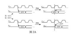
圖2A為根據本案一些實施例示出圖1的資料訊號SD1'出現右偏移的波形示意圖。接收器電路102自發射器電路12接收時脈訊號CK1以做為時脈訊號CK1',且發射器電路12響應於時脈訊號CK1的負緣傳輸資料訊號SD1至接收器電路102。接收器電路102根據時脈訊號CK1'的正緣對資料訊號SD1'取樣以產生資料訊號SD2(未繪示)。若線路延遲(例如為電路板引入的延遲)的影響不大(即第一情形),時脈訊號CK1'的正緣可對齊到資料訊號SD1'的有效區間(例如為眼圖中心)。於此條件下,接收器電路102可產生出正確的資料訊號SD2。FIG. 2A is a schematic diagram of a waveform showing a right shift of the data signal SD1 ′ of FIG. 1 according to some embodiments of the present invention. The
或者,若時脈訊號CK1過快(即第二情形),時脈訊號CK1'的正緣早於資料訊號SD1'的有效區間。於此條件下,接收器電路102會產生錯誤的資料訊號SD2,且偏移偵測電路110判斷資料訊號SD1'具有右偏移。舉例來說,若資料訊號SD1為00100,資料訊號SD2亦應為00100。在第二情形的例子中,由於接收器電路102過早對資料訊號SD1'取樣,資料訊號SD2會誤變為00010。相較於資料訊號SD1,資料訊號SD1'(或資料訊號SD2)出現右偏移。Alternatively, if the clock signal CK1 is too fast (ie, the second case), the positive edge of the clock signal CK1 ' is earlier than the valid period of the data signal SD1 '. Under this condition, the
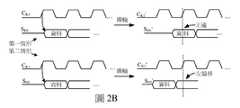
圖2B為根據本案一些實施例示出圖1的資料訊號SD1'出現左偏移的波形示意圖。於此例中,發射器電路12響應於時脈訊號CK1的正緣傳輸資料訊號SD1至接收器電路102。接收器電路102根據時脈訊號CK1'的正緣對資料訊號SD1'取樣以產生資料訊號SD2(未繪示)。若線路延遲的影響不大(即第一情形),時脈訊號CK1'的正緣可對齊到資料訊號SD1'的有效區間。於此條件下,接收器電路102可產生出正確的資料訊號SD2。FIG. 2B is a schematic diagram of a waveform showing a left shift of the data signal SD1 ′ of FIG. 1 according to some embodiments of the present invention. In this example, the
或者,若線路延遲的影響過大(即第二情形),時脈訊號CK1'的正緣晚於資料訊號SD1'的有效區間。於此條件下,接收器電路102會產生錯誤的資料訊號SD2,且偏移偵測電路110判斷資料訊號SD1'具有左偏移。舉例來說,由於接收器電路102過晚對資料訊號SD1'取樣,資料訊號SD2會誤變為01000。相較於資料訊號SD1,資料訊號SD1'(或資料訊號SD2)出現左偏移。Alternatively, if the influence of the line delay is too great (ie, the second case), the positive edge of the clock signal CK1 ' is later than the valid period of the data signal SD1 '. Under this condition, the
繼續參照圖1。於一些實施例中,偏移偵測電路110可包含暫存器(未繪示),其用以儲存該些符記TO1~TOn。舉例來說,多個符記TO1~TOn可由下表之形式儲存於此暫存器:
於此例中,n設置為6,且每一個符記TO1~TOn設定為具有8個位元,其中最右位元為第0個位元,且最左位元為第7個位元。於一些實施例中,每一個符記TO1~TO6包含至少一預設邏輯值(例如可為邏輯值1),且每一個符記TO1~TO6的至少一預設邏輯值之個數彼此不同。於此例中,多個符記TO1~TO6的邏輯值1之個數依序遞增。詳細而言,符記TO1的第5個位元為邏輯值1(即邏輯值1之個數為1),符記TO2的第4~5個位元為邏輯值1(即邏輯值1之個數為2),且符記TO3的第4~6個位元為邏輯值1(即邏輯值1之個數為3)。依此類推,可推得符記TO6的位元設定方式。In this example, n is set to 6, and each token TO1 ~TOn is set to have 8 bits, of which the rightmost bit is the 0th bit, and the leftmost bit is the 7th bit Yuan. In some embodiments, each token TO1 ˜TO6 includes at least one predetermined logic value (for example, a logic value 1), and each token TO1 ˜TO6 has one of at least one predetermined logic value The numbers are different from each other. In this example, the number of logical values 1 of a plurality of symbols TO1 to TO6 increases sequentially. In detail, the 5th bit of the symbol TO1 is a logical value 1 (that is, the number of logical value 1s is 1), and the 4th to 5th bits of the symbol TO2 are a logical value 1 (that is, the logical value The number of 1 is 2), and the 4th to 6th bits of the symbol TO3 are logical value 1 (that is, the number of logical value 1 is 3). By analogy, the bit setting method of symbol TO6 can be deduced.
如圖1所示,資料訊號SD1可包含符記、有效資料(payload)以及偽(dummy)符記。符記為主機裝置10與串列資料處理裝置100預先決定好的特定編碼,並為資料訊號SD1的前置資料。有效資料為主機裝置10欲傳輸的真實資料。偽符記為發生右偏移時的緩衝符記資料。As shown in FIG. 1 , the data signal SD1 may include tokens, payloads and dummy tokens. The symbol is a specific code pre-determined by the
於連線初始階段,主機裝置10與串列資料處理裝置100可事先約定使用多個符記TO1~TO6中之一者來進行連線,以偵測後續的傳輸過程中是否會出現偏移。在資料訊號SD1的符記中,至少一預定邏輯值之個數為第一個數。在多個符記TO1~TO6之對應者中,至少一預定邏輯值之個數為第二個數,且第一個數相同於第二個數。In the initial stage of connection, the
舉例來說,主機裝置10使用包含符記TO1的資料訊號SD1來與串列資料處理裝置100進行連線。偏移偵測電路110可根據資料訊號SD2的前8位元資料與多個符記TO1~TOn中之對應者進行比較,以偵測偏移為左偏移或右偏移。若不存在偏移,資料訊號SD2的前8位元資料相同於資料訊號SD1的符記TO1。偏移偵測電路110可根據至少一預設邏輯值(例如為邏輯值1)在多個符記TO1~TOn之對應者中的位元位置以及至少一預設邏輯值在資料訊號SD2的前8位元資料中之位元位置確認偏移為左偏移或右偏移。For example, the
例如,若資料訊號SD2(即取樣到的資料訊號SD1')的前8位元資料為00001000(即第一個數為1),偏移偵測電路110可自多個符記TO1~TOn中選出僅包含1個邏輯值1(即第二個數為1)的符記TO1,並將此8位元資料00001000與符記TO1進行比較。在符記TO1中,第5個位元為邏輯值1。在8位元資料00001000中,第4個位元為邏輯值1。於此情形下,偏移偵測電路110可判斷資料訊號SD1'出現右偏移,且偏移量為1個位元。偏移偵測電路110可據此輸出具有第一數值的修正訊號SA至偏移校正電路120。For example, if the first 8-bit data of the data signal SD2 (ie, the sampled data signal SD1 ′) is 00001000 (ie, the first number is 1), the offset
或者,若資料訊號SD2的前8位元資料為00100000,偏移偵測電路110可自多個符記TO1~TOn中選出僅包含1個邏輯值1的符記TO1,並將此8個位元資料00100000與符記TO1進行比較。在符記TO1中,第5個位元為邏輯值1。在8位元資料00100000中,第6個位元為邏輯值1。於此情形下,偏移偵測電路110可判斷資料訊號SD1'出現左偏移,且偏移量為1個位元。偏移偵測電路110可據此輸出具有第二數值的修正訊號SA至偏移校正電路120。Alternatively, if the first 8 bits of data of the data signal SD2 are 00100000, the offset
響應於修正訊號SA,偏移校正電路120可修正資料訊號SD2之偏移以產生資料訊號SD3。舉例而言,若偵測到偏移為右偏移且偏移量為1位元,偏移校正電路120可將所收到的資料訊號SD2之位元向左位移1位元,並輸出為資料訊號SD3。如此一來,處理電路130可接收到正確的有效資料。In response to the correction signal SA , the offset
於一些實施例中,偏移偵測電路110可包含暫存器電路、比較器電路(例如可為互斥或閘電路)、計數器電路與/或其他數位邏輯電路,以實施儲存多個符記TO1~TOn與偵測資料偏移的操作。於一些實施例中,偏移校正電路120可包含移位暫存器電路與/或一或多個數位邏輯電路,以實施校正偏移的操作。於一些實施例中,偏移校正電路120中之數位邏輯電路可設定為(但不限於)執行位元(bitwise)運算,以實施位元移位的操作。上述關於偏移偵測電路110與偏移校正電路120的實施方式用於示例,且本案並不以此為限。In some embodiments, the offset
圖3為根據本案一些實施例示出圖1的資料訊號SDO的波形圖。如前所述,若偵測到右偏移,代表時脈訊號CK1可能過快。如先前圖1所示,接收器電路14根據時脈訊號CK1取樣接收到的資料訊號SDO(後稱資料訊號SDO')。如圖3所示,若時脈訊號CK1的頻率過高且接收器電路14根據時脈訊號CK1的正緣取樣資料訊號SDO'時(即第一情形),時脈訊號CK1的正緣早於資料訊號SDO'的有效區間而取樣到錯誤的資料。FIG. 3 is a waveform diagram illustrating the data signal SDO of FIG. 1 according to some embodiments of the present invention. As mentioned above, if a right offset is detected, it means that the clock signal CK1 may be too fast. As previously shown in FIG. 1 , the receiver circuit 14 samples the received data signal SDO (hereinafter referred to as the data signal SDO ′) according to the clock signal CK1 . As shown in FIG. 3 , if the frequency of the clock signal CK1 is too high and the receiver circuit 14 samples the data signal SDO ′ according to the positive edge of the clock signal CK1 (ie, the first case), the frequency of the clock signal CK1 The positive edge samples the wrong data earlier than the valid interval of the data signal SDO '.
於本案一些實施例中,當偏移偵測電路110偵測到資料訊號SD1'出現右偏移,偏移偵測電路110更用以輸出控制訊號SC至發射器電路104,以提高發射器電路104的驅動能力(即圖3的第二情形)。例如,發射器電路104可根據控制訊號SC提升資料訊號SDO的電流。如此,時脈訊號CK1的正緣可對齊資料訊號SDO'的有效區間而取樣到正確的資料。於一些實施例中,發射器電路104的偏壓設定與/或負載設定可響應於控制訊號SC調整,以實施上述調整驅動能力之操作。In some embodiments of the present application, when the offset
圖4為根據本案一些實施例示出一種串列資料處理裝置100的示意圖。相較於圖1,如下表所示,多個符記TO1~TOn每一者對應於一預設指令。換言之,多個符記TO1~TOn每一者內嵌一組對應於預設指令的運算程式碼(operation code)。藉由上述設置方式,在傳送用於偵測偏移的符記時,主機裝置10可提供欲由串列資料處理裝置100執行的指令。FIG. 4 is a schematic diagram illustrating a serial


於此例中,偏移偵測電路110更根據資料訊號SD1的符記所對應的預設指令產生指令訊號SI1。例如,偏移偵測電路110根據資料訊號SD1'的前8個位元資料解出前述的運算程式碼為指令訊號SI1。偏移校正電路120更根據修正訊號SA修正指令訊號SI1以產生指令訊號SI2。指令訊號SI2用於通知處理電路130執行預設指令所對應之操作。偏移偵測電路110可根據資料訊號SD1'的前8個位元資料中至少一預設值的數量而自上表中選出一符記,並根據該符記對應的預設指令產生指令訊號SI1。舉例來說,若資料訊號SD1'的前8個位元資料包含1個邏輯值1,偏移偵測電路110可選出符記TO1,並輸出符記TO1對應的記憶體讀取指令為指令訊號SI1。偏移校正電路120可根據修正訊號SA來修正指令訊號SI1,以產生正確的指令訊號SI2。如此,處理電路130可根據指令訊號SI2執行記憶體讀取的操作。In this example, the offset
於一些應用中,處理電路130的操作為平行運算。在此些應用中,串列資料處理裝置100可設定為輸出並列資料。圖5A為根據本案一些實施例示出串列資料處理裝置100的示意圖。於此例中,串列資料處理裝置100更包含串列轉並列(serial-to-parallel)電路510。串列轉並列電路510耦接於偏移偵測電路110與偏移校正電路120之間,並用以根據資料訊號SD1'產生多個資料訊號SD4,並根據指令訊號SI1產生多個指令訊號SI3。偏移校正電路120根據修正訊號SA修正多個資料訊號SD4以產生資料訊號SD3,並修正多個指令訊號SI3以產生指令訊號SI2。In some applications, the operations of the
圖5B為根據本案一些實施例示出串列資料處理裝置100的示意圖。相較於圖5A,串列轉並列電路510耦接於偏移校正電路120與處理電路130之間。串列轉並列電路510根據資料訊號SD3產生多個資料訊號SD5,並根據指令訊號SI2產生多個指令訊號SI4。FIG. 5B is a schematic diagram illustrating the serial
圖6為根據本案一些實施例示出一種資料偏移修正方法600的流程圖。於一些實施例中,資料偏移修正方法600可由(但不限於)串列資料處理裝置100執行。FIG. 6 is a flowchart illustrating a data offset
於操作S610,自主機裝置接收第一資料訊號。In operation S610, a first data signal is received from the host device.
於操作S620,根據複數個符記偵測接收到的第一資料訊號的偏移以產生修正訊號,其中該些符記中每一者包含至少一預設邏輯值,且該些符記中每一者的該至少一預設邏輯值的個數彼此不同。In operation S620, an offset of the received first data signal is detected according to a plurality of symbols to generate a correction signal, wherein each of the symbols includes at least a predetermined logic value, and each of the symbols The numbers of the at least one default logic value of one are different from each other.
於操作S630,根據修正訊號修正接收到的第一資料訊號,以產生第二資料訊號。In operation S630, the received first data signal is modified according to the modification signal to generate a second data signal.
上述操作S610、S620以及S630之說明可參照前述各個實施例,故不重複贅述。上述資料偏移修正方法600的多個操作僅為示例,並非限定需依照此示例中的順序執行。在不違背本案的各實施例的操作方式與範圍下,在資料偏移修正方法600下的各種操作當可適當地增加、替換、省略或以不同順序執行。The description of the above operations S610 , S620 and S630 may refer to the foregoing embodiments, and thus will not be repeated. The operations of the above data offset
上述關於符記的設置方式以及位元數量用於示例,且本案各實施例並不以上述例子為限。The above-mentioned setting manner of the mark and the number of bits are used as examples, and the embodiments of the present application are not limited to the above-mentioned examples.
綜上所述,本案一些實施例所提供的串列資料處理裝置與資料偏移修正方法可利用預先設定好的多種符記修正資料偏移。於進一步的實施例中,這些符記更可用於傳輸預設指令。To sum up, the serial data processing apparatus and data offset correction method provided by some embodiments of the present application can correct the data offset by using a variety of preset symbols. In further embodiments, these tokens may be used to transmit preset commands.
雖然本案之實施例如上所述,然而該些實施例並非用來限定本案,本技術領域具有通常知識者可依據本案之明示或隱含之內容對本案之技術特徵施以變化,凡此種變化均可能屬於本案所尋求之專利保護範疇,換言之,本案之專利保護範圍須視本說明書之申請專利範圍所界定者為準。Although the embodiments of the present case are as described above, these embodiments are not intended to limit the present case. Those with ordinary knowledge in the technical field can interpret the technology of the present case based on the explicit or implicit content of the present case.Changes in features may fall within the scope of patent protection sought in this case. In other words, the scope of patent protection in this case must be determined by the scope of the patent application in this specification.
10:主機裝置10: Host device
12:發射器電路12: Transmitter circuit
14:接收器電路14: Receiver circuit
100:串列資料處理裝置100: Serial data processing device
102:接收器電路102: Receiver circuit
104:發射器電路104: Transmitter circuit
110:偏移偵測電路110: Offset detection circuit
120:偏移校正電路120: Offset correction circuit
130:處理電路130: Processing circuit
CK1、CK1':時脈訊號CK1 , CK1 ': clock signal
SA:修正訊號SA : Correction signal
SC:控制訊號SC : Control signal
SD1,SD1',SD2,SD3,SDO,SDO':資料訊號SD1 , SD1 ', SD2 , SD3 , SDO , SDO ': data signal
TO1~TOn:符記TO1 ~TOn : notation
Claims (10)
Translated fromChinesePriority Applications (2)
| Application Number | Priority Date | Filing Date | Title |
|---|---|---|---|
| TW109102229ATWI768284B (en) | 2020-01-21 | 2020-01-21 | Serial data processing device and data offset calibration method |
| US17/138,969US11372799B2 (en) | 2020-01-21 | 2020-12-31 | Serial data processing device and data offset calibration method |
Applications Claiming Priority (1)
| Application Number | Priority Date | Filing Date | Title |
|---|---|---|---|
| TW109102229ATWI768284B (en) | 2020-01-21 | 2020-01-21 | Serial data processing device and data offset calibration method |
Publications (2)
| Publication Number | Publication Date |
|---|---|
| TW202129641A TW202129641A (en) | 2021-08-01 |
| TWI768284Btrue TWI768284B (en) | 2022-06-21 |
Family
ID=76856989
Family Applications (1)
| Application Number | Title | Priority Date | Filing Date |
|---|---|---|---|
| TW109102229ATWI768284B (en) | 2020-01-21 | 2020-01-21 | Serial data processing device and data offset calibration method |
Country Status (2)
| Country | Link |
|---|---|
| US (1) | US11372799B2 (en) |
| TW (1) | TWI768284B (en) |
Families Citing this family (2)
| Publication number | Priority date | Publication date | Assignee | Title |
|---|---|---|---|---|
| JP7004392B2 (en)* | 2020-02-05 | 2022-01-21 | Necプラットフォームズ株式会社 | Time synchronization device, time synchronization system and time synchronization method |
| US12231527B2 (en)* | 2021-06-22 | 2025-02-18 | Texas Instruments Incorporated | Clock recovery training |
Citations (4)
| Publication number | Priority date | Publication date | Assignee | Title |
|---|---|---|---|---|
| US5473610A (en)* | 1993-04-22 | 1995-12-05 | France Telecom | Method of clock signal recovery and of synchronization for the reception of information elements transmitted by an ATM network and device for the implementation of the method |
| TW201230311A (en)* | 2010-06-30 | 2012-07-16 | Life Technologies Corp | Array column integrator |
| CN103004118A (en)* | 2010-12-10 | 2013-03-27 | 松下电器产业株式会社 | Precoding method and sending device |
| US10045078B2 (en)* | 2007-07-02 | 2018-08-07 | Lg Electronics Inc. | Digital broadcasting system and data processing method |
Family Cites Families (6)
| Publication number | Priority date | Publication date | Assignee | Title |
|---|---|---|---|---|
| US20020184412A1 (en)* | 2001-06-02 | 2002-12-05 | Stevens James Ray | System and method for locating and aligning to framing bits |
| JP4652961B2 (en)* | 2005-11-30 | 2011-03-16 | 富士通株式会社 | Serial transfer interface |
| JP5531655B2 (en)* | 2010-02-08 | 2014-06-25 | 富士通株式会社 | Serial data receiving circuit device and serial data receiving method |
| JP5488330B2 (en)* | 2010-08-18 | 2014-05-14 | 富士通株式会社 | Signal shaping circuit and optical transmitter |
| WO2013039624A1 (en)* | 2011-09-12 | 2013-03-21 | Rambus Inc. | Offset and decision feedback equalization calibration |
| US9100094B2 (en)* | 2013-04-25 | 2015-08-04 | Nvidia Corporation | System and method for tuning a serial link |
- 2020
- 2020-01-21TWTW109102229Apatent/TWI768284B/enactive
- 2020-12-31USUS17/138,969patent/US11372799B2/enactiveActive
Patent Citations (4)
| Publication number | Priority date | Publication date | Assignee | Title |
|---|---|---|---|---|
| US5473610A (en)* | 1993-04-22 | 1995-12-05 | France Telecom | Method of clock signal recovery and of synchronization for the reception of information elements transmitted by an ATM network and device for the implementation of the method |
| US10045078B2 (en)* | 2007-07-02 | 2018-08-07 | Lg Electronics Inc. | Digital broadcasting system and data processing method |
| TW201230311A (en)* | 2010-06-30 | 2012-07-16 | Life Technologies Corp | Array column integrator |
| CN103004118A (en)* | 2010-12-10 | 2013-03-27 | 松下电器产业株式会社 | Precoding method and sending device |
Also Published As
| Publication number | Publication date |
|---|---|
| US11372799B2 (en) | 2022-06-28 |
| US20210224218A1 (en) | 2021-07-22 |
| TW202129641A (en) | 2021-08-01 |
Similar Documents
| Publication | Publication Date | Title |
|---|---|---|
| CN111354390B (en) | Memory system, operation method of memory system and memory controller | |
| US7307461B2 (en) | System and method for adaptive duty cycle optimization | |
| US8667194B2 (en) | Two-wire interface in which a master component monitors the data line during the preamble generation phase for synchronization with one or more slave components | |
| EP2141848B1 (en) | Error detection in high speed asymmetric interfaces using dedicated interface lines | |
| US10089173B2 (en) | Error detection constants of symbol transition clocking transcoding | |
| TWI768284B (en) | Serial data processing device and data offset calibration method | |
| US10972248B2 (en) | Method of calibrating clock phase and voltage offset, data recovery circuit performing the same and receiver including the same | |
| CN104835534B (en) | Semiconductor storage and its operating method | |
| US8045667B2 (en) | Deserializer and data recovery method | |
| CN105955915B (en) | A kind of parallel data goes the method, apparatus and system of deflection | |
| EP4616295A1 (en) | In-band data package transmission | |
| JP2010212989A (en) | Address decoder and address setting method | |
| US8184680B2 (en) | Data transceiver system and associated methods | |
| CN112118441A (en) | Bit correction improved serial CMOS image data training method | |
| US9484949B1 (en) | Variable run length encoding of a bit stream | |
| CN115705264A (en) | Semiconductor system and electronic device associated with performing a training operation | |
| CN113204504B (en) | Serial data processing apparatus and data offset correction method | |
| CN114756499B (en) | Phase calibration method and system | |
| US9275758B2 (en) | Error detection circuit and semiconductor integrated circuit using the same | |
| US12067294B2 (en) | Interface circuit for converting a serial data stream to a parallel data scheme with data strobe preamble information in the serial data stream | |
| US20230087104A1 (en) | Signal processing circuit and reception device | |
| TWI895016B (en) | Signal receiving circuit, memory storage device and reference voltage adjustment method | |
| US20050132247A1 (en) | Two-wire interface having embedded per frame reliability information | |
| US11296697B1 (en) | On-die termination circuit, operating method thereof, and semiconductor system | |
| US20240413929A1 (en) | Method and apparatus for generating error correcting codes with transition encoding |