TWI767512B - Cool electron erasing in thin-film storage transistors - Google Patents
Cool electron erasing in thin-film storage transistorsDownload PDFInfo
- Publication number
- TWI767512B TWI767512BTW110101376ATW110101376ATWI767512BTW I767512 BTWI767512 BTW I767512BTW 110101376 ATW110101376 ATW 110101376ATW 110101376 ATW110101376 ATW 110101376ATW I767512 BTWI767512 BTW I767512B
- Authority
- TW
- Taiwan
- Prior art keywords
- storage transistor
- layer
- charge trapping
- dielectric layer
- tunneling
- Prior art date
Links
- 239000010409thin filmSubstances0.000titleclaimsdescription11
- 230000005641tunnelingEffects0.000claimsabstractdescription96
- 230000004888barrier functionEffects0.000claimsabstractdescription46
- VYPSYNLAJGMNEJ-UHFFFAOYSA-NSilicium dioxideChemical compoundO=[Si]=OVYPSYNLAJGMNEJ-UHFFFAOYSA-N0.000claimsdescription53
- 229910052581Si3N4Inorganic materials0.000claimsdescription28
- HQVNEWCFYHHQES-UHFFFAOYSA-Nsilicon nitrideChemical compoundN12[Si]34N5[Si]62N3[Si]51N64HQVNEWCFYHHQES-UHFFFAOYSA-N0.000claimsdescription26
- 230000000903blocking effectEffects0.000claimsdescription25
- 239000000463materialSubstances0.000claimsdescription20
- 229910052710siliconInorganic materials0.000claimsdescription20
- XUIMIQQOPSSXEZ-UHFFFAOYSA-NSiliconChemical compound[Si]XUIMIQQOPSSXEZ-UHFFFAOYSA-N0.000claimsdescription18
- 239000010703siliconSubstances0.000claimsdescription18
- TWNQGVIAIRXVLR-UHFFFAOYSA-Noxo(oxoalumanyloxy)alumaneChemical compoundO=[Al]O[Al]=OTWNQGVIAIRXVLR-UHFFFAOYSA-N0.000claimsdescription16
- 229910052814silicon oxideInorganic materials0.000claimsdescription11
- CETPSERCERDGAM-UHFFFAOYSA-Nceric oxideChemical compoundO=[Ce]=OCETPSERCERDGAM-UHFFFAOYSA-N0.000claimsdescription10
- 229910000422cerium(IV) oxideInorganic materials0.000claimsdescription9
- 230000015654memoryEffects0.000claimsdescription8
- 229910052751metalInorganic materials0.000claimsdescription8
- 239000002184metalSubstances0.000claimsdescription8
- BASFCYQUMIYNBI-UHFFFAOYSA-NplatinumChemical compound[Pt]BASFCYQUMIYNBI-UHFFFAOYSA-N0.000claimsdescription8
- MCMNRKCIXSYSNV-UHFFFAOYSA-NZrO2Inorganic materialsO=[Zr]=OMCMNRKCIXSYSNV-UHFFFAOYSA-N0.000claimsdescription7
- 239000003989dielectric materialSubstances0.000claimsdescription7
- CBENFWSGALASAD-UHFFFAOYSA-NOzoneChemical compound[O-][O+]=OCBENFWSGALASAD-UHFFFAOYSA-N0.000claimsdescription6
- GWEVSGVZZGPLCZ-UHFFFAOYSA-NTitan oxideChemical compoundO=[Ti]=OGWEVSGVZZGPLCZ-UHFFFAOYSA-N0.000claimsdescription6
- BPUBBGLMJRNUCC-UHFFFAOYSA-Noxygen(2-);tantalum(5+)Chemical compound[O-2].[O-2].[O-2].[O-2].[O-2].[Ta+5].[Ta+5]BPUBBGLMJRNUCC-UHFFFAOYSA-N0.000claimsdescription5
- RVTZCBVAJQQJTK-UHFFFAOYSA-Noxygen(2-);zirconium(4+)Chemical compound[O-2].[O-2].[Zr+4]RVTZCBVAJQQJTK-UHFFFAOYSA-N0.000claimsdescription5
- PBCFLUZVCVVTBY-UHFFFAOYSA-Ntantalum pentoxideInorganic materialsO=[Ta](=O)O[Ta](=O)=OPBCFLUZVCVVTBY-UHFFFAOYSA-N0.000claimsdescription5
- QGZKDVFQNNGYKY-UHFFFAOYSA-NAmmoniaChemical compoundNQGZKDVFQNNGYKY-UHFFFAOYSA-N0.000claimsdescription4
- KJTLSVCANCCWHF-UHFFFAOYSA-NRutheniumChemical compound[Ru]KJTLSVCANCCWHF-UHFFFAOYSA-N0.000claimsdescription4
- 229910006501ZrSiOInorganic materials0.000claimsdescription4
- 229910017052cobaltInorganic materials0.000claimsdescription4
- 239000010941cobaltSubstances0.000claimsdescription4
- GUTLYIVDDKVIGB-UHFFFAOYSA-Ncobalt atomChemical compound[Co]GUTLYIVDDKVIGB-UHFFFAOYSA-N0.000claimsdescription4
- 230000006870functionEffects0.000claimsdescription4
- CJNBYAVZURUTKZ-UHFFFAOYSA-Nhafnium(iv) oxideChemical compoundO=[Hf]=OCJNBYAVZURUTKZ-UHFFFAOYSA-N0.000claimsdescription4
- 229910052697platinumInorganic materials0.000claimsdescription4
- 229910052707rutheniumInorganic materials0.000claimsdescription4
- VEALVRVVWBQVSL-UHFFFAOYSA-Nstrontium titanateChemical compound[Sr+2].[O-][Ti]([O-])=OVEALVRVVWBQVSL-UHFFFAOYSA-N0.000claimsdescription4
- GFQYVLUOOAAOGM-UHFFFAOYSA-Nzirconium(iv) silicateChemical compound[Zr+4].[O-][Si]([O-])([O-])[O-]GFQYVLUOOAAOGM-UHFFFAOYSA-N0.000claimsdescription4
- 238000000137annealingMethods0.000claimsdescription3
- SIWVEOZUMHYXCS-UHFFFAOYSA-Noxo(oxoyttriooxy)yttriumChemical compoundO=[Y]O[Y]=OSIWVEOZUMHYXCS-UHFFFAOYSA-N0.000claimsdescription3
- 229910021420polycrystalline siliconInorganic materials0.000claimsdescription3
- 229920005591polysiliconPolymers0.000claimsdescription3
- 229910021529ammoniaInorganic materials0.000claimsdescription2
- 239000001257hydrogenSubstances0.000claimsdescription2
- 229910052739hydrogenInorganic materials0.000claimsdescription2
- 125000004435hydrogen atomChemical class[H]*0.000claimsdescription2
- MRELNEQAGSRDBK-UHFFFAOYSA-Nlanthanum(3+);oxygen(2-)Chemical compound[O-2].[O-2].[O-2].[La+3].[La+3]MRELNEQAGSRDBK-UHFFFAOYSA-N0.000claimsdescription2
- HWEYZGSCHQNNEH-UHFFFAOYSA-Nsilicon tantalumChemical compound[Si].[Ta]HWEYZGSCHQNNEH-UHFFFAOYSA-N0.000claimsdescription2
- MZLGASXMSKOWSE-UHFFFAOYSA-Ntantalum nitrideChemical compound[Ta]#NMZLGASXMSKOWSE-UHFFFAOYSA-N0.000claimsdescription2
- WFKWXMTUELFFGS-UHFFFAOYSA-NtungstenChemical compound[W]WFKWXMTUELFFGS-UHFFFAOYSA-N0.000claimsdescription2
- 229910052721tungstenInorganic materials0.000claimsdescription2
- 239000010937tungstenSubstances0.000claimsdescription2
- 239000005543nano-size silicon particleSubstances0.000claims1
- AZCUJQOIQYJWQJ-UHFFFAOYSA-Noxygen(2-) titanium(4+) trihydrateChemical compound[O-2].[O-2].[Ti+4].O.O.OAZCUJQOIQYJWQJ-UHFFFAOYSA-N0.000claims1
- 238000004151rapid thermal annealingMethods0.000claims1
- 239000002210silicon-based materialSubstances0.000claims1
- 238000010079rubber tappingMethods0.000abstract1
- 235000012239silicon dioxideNutrition0.000description21
- 239000000377silicon dioxideSubstances0.000description21
- 239000000758substrateSubstances0.000description20
- 238000010586diagramMethods0.000description13
- 238000000034methodMethods0.000description10
- 230000007246mechanismEffects0.000description7
- 238000000231atomic layer depositionMethods0.000description6
- 230000007547defectEffects0.000description6
- 230000005684electric fieldEffects0.000description6
- 238000004088simulationMethods0.000description6
- 238000003786synthesis reactionMethods0.000description6
- 229910018072Al 2 O 3Inorganic materials0.000description4
- 229910004298SiO 2Inorganic materials0.000description4
- 230000008901benefitEffects0.000description4
- 238000002347injectionMethods0.000description4
- 239000007924injectionSubstances0.000description4
- 230000014759maintenance of locationEffects0.000description4
- 230000003647oxidationEffects0.000description4
- 238000007254oxidation reactionMethods0.000description4
- 230000008569processEffects0.000description4
- 230000015572biosynthetic processEffects0.000description3
- 230000015556catabolic processEffects0.000description3
- 230000006378damageEffects0.000description3
- 239000004065semiconductorSubstances0.000description3
- 230000002411adverseEffects0.000description2
- PNEYBMLMFCGWSK-UHFFFAOYSA-Naluminium oxideInorganic materials[O-2].[O-2].[O-2].[Al+3].[Al+3]PNEYBMLMFCGWSK-UHFFFAOYSA-N0.000description2
- QVGXLLKOCUKJST-UHFFFAOYSA-Natomic oxygenChemical compound[O]QVGXLLKOCUKJST-UHFFFAOYSA-N0.000description2
- 238000006731degradation reactionMethods0.000description2
- 230000005527interface trapEffects0.000description2
- 239000001301oxygenSubstances0.000description2
- 229910052760oxygenInorganic materials0.000description2
- 230000005689Fowler Nordheim tunnelingEffects0.000description1
- 240000007594Oryza sativaSpecies0.000description1
- 235000007164Oryza sativaNutrition0.000description1
- 238000003491arrayMethods0.000description1
- 230000009286beneficial effectEffects0.000description1
- 230000008859changeEffects0.000description1
- 230000001627detrimental effectEffects0.000description1
- 230000000694effectsEffects0.000description1
- 150000002739metalsChemical class0.000description1
- 230000004048modificationEffects0.000description1
- 238000012986modificationMethods0.000description1
- 239000002071nanotubeSubstances0.000description1
- 230000000149penetrating effectEffects0.000description1
- 230000002688persistenceEffects0.000description1
- 235000009566riceNutrition0.000description1
- 230000001568sexual effectEffects0.000description1
- 210000000352storage cellAnatomy0.000description1
- 239000004408titanium dioxideSubstances0.000description1
- 229910052727yttriumInorganic materials0.000description1
- VWQVUPCCIRVNHF-UHFFFAOYSA-Nyttrium atomChemical compound[Y]VWQVUPCCIRVNHF-UHFFFAOYSA-N0.000description1
Images


Classifications
- H—ELECTRICITY
- H10—SEMICONDUCTOR DEVICES; ELECTRIC SOLID-STATE DEVICES NOT OTHERWISE PROVIDED FOR
- H10D—INORGANIC ELECTRIC SEMICONDUCTOR DEVICES
- H10D64/00—Electrodes of devices having potential barriers
- H10D64/01—Manufacture or treatment
- H10D64/031—Manufacture or treatment of data-storage electrodes
- H10D64/037—Manufacture or treatment of data-storage electrodes comprising charge-trapping insulators
- H—ELECTRICITY
- H10—SEMICONDUCTOR DEVICES; ELECTRIC SOLID-STATE DEVICES NOT OTHERWISE PROVIDED FOR
- H10D—INORGANIC ELECTRIC SEMICONDUCTOR DEVICES
- H10D30/00—Field-effect transistors [FET]
- H10D30/60—Insulated-gate field-effect transistors [IGFET]
- H10D30/69—IGFETs having charge trapping gate insulators, e.g. MNOS transistors
- G—PHYSICS
- G11—INFORMATION STORAGE
- G11C—STATIC STORES
- G11C16/00—Erasable programmable read-only memories
- G11C16/02—Erasable programmable read-only memories electrically programmable
- G11C16/06—Auxiliary circuits, e.g. for writing into memory
- G11C16/10—Programming or data input circuits
- G—PHYSICS
- G11—INFORMATION STORAGE
- G11C—STATIC STORES
- G11C16/00—Erasable programmable read-only memories
- G11C16/02—Erasable programmable read-only memories electrically programmable
- G11C16/06—Auxiliary circuits, e.g. for writing into memory
- G11C16/10—Programming or data input circuits
- G11C16/14—Circuits for erasing electrically, e.g. erase voltage switching circuits
- H—ELECTRICITY
- H10—SEMICONDUCTOR DEVICES; ELECTRIC SOLID-STATE DEVICES NOT OTHERWISE PROVIDED FOR
- H10B—ELECTRONIC MEMORY DEVICES
- H10B43/00—EEPROM devices comprising charge-trapping gate insulators
- H10B43/30—EEPROM devices comprising charge-trapping gate insulators characterised by the memory core region
- H—ELECTRICITY
- H10—SEMICONDUCTOR DEVICES; ELECTRIC SOLID-STATE DEVICES NOT OTHERWISE PROVIDED FOR
- H10D—INORGANIC ELECTRIC SEMICONDUCTOR DEVICES
- H10D30/00—Field-effect transistors [FET]
- H10D30/60—Insulated-gate field-effect transistors [IGFET]
- H10D30/69—IGFETs having charge trapping gate insulators, e.g. MNOS transistors
- H10D30/694—IGFETs having charge trapping gate insulators, e.g. MNOS transistors characterised by the shapes, relative sizes or dispositions of the gate electrodes
- H—ELECTRICITY
- H10—SEMICONDUCTOR DEVICES; ELECTRIC SOLID-STATE DEVICES NOT OTHERWISE PROVIDED FOR
- H10D—INORGANIC ELECTRIC SEMICONDUCTOR DEVICES
- H10D64/00—Electrodes of devices having potential barriers
- H10D64/60—Electrodes characterised by their materials
- H10D64/66—Electrodes having a conductor capacitively coupled to a semiconductor by an insulator, e.g. MIS electrodes
- H10D64/68—Electrodes having a conductor capacitively coupled to a semiconductor by an insulator, e.g. MIS electrodes characterised by the insulator, e.g. by the gate insulator
- H10D64/681—Electrodes having a conductor capacitively coupled to a semiconductor by an insulator, e.g. MIS electrodes characterised by the insulator, e.g. by the gate insulator having a compositional variation, e.g. multilayered
- H10D64/685—Electrodes having a conductor capacitively coupled to a semiconductor by an insulator, e.g. MIS electrodes characterised by the insulator, e.g. by the gate insulator having a compositional variation, e.g. multilayered being perpendicular to the channel plane
- H—ELECTRICITY
- H10—SEMICONDUCTOR DEVICES; ELECTRIC SOLID-STATE DEVICES NOT OTHERWISE PROVIDED FOR
- H10D—INORGANIC ELECTRIC SEMICONDUCTOR DEVICES
- H10D64/00—Electrodes of devices having potential barriers
- H10D64/60—Electrodes characterised by their materials
- H10D64/66—Electrodes having a conductor capacitively coupled to a semiconductor by an insulator, e.g. MIS electrodes
- H10D64/68—Electrodes having a conductor capacitively coupled to a semiconductor by an insulator, e.g. MIS electrodes characterised by the insulator, e.g. by the gate insulator
- H10D64/691—Electrodes having a conductor capacitively coupled to a semiconductor by an insulator, e.g. MIS electrodes characterised by the insulator, e.g. by the gate insulator comprising metallic compounds, e.g. metal oxides or metal silicates
- H—ELECTRICITY
- H10—SEMICONDUCTOR DEVICES; ELECTRIC SOLID-STATE DEVICES NOT OTHERWISE PROVIDED FOR
- H10D—INORGANIC ELECTRIC SEMICONDUCTOR DEVICES
- H10D30/00—Field-effect transistors [FET]
- H10D30/60—Insulated-gate field-effect transistors [IGFET]
- H10D30/68—Floating-gate IGFETs
- H10D30/681—Floating-gate IGFETs having only two programming levels
- H10D30/683—Floating-gate IGFETs having only two programming levels programmed by tunnelling of carriers, e.g. Fowler-Nordheim tunnelling
- H—ELECTRICITY
- H10—SEMICONDUCTOR DEVICES; ELECTRIC SOLID-STATE DEVICES NOT OTHERWISE PROVIDED FOR
- H10D—INORGANIC ELECTRIC SEMICONDUCTOR DEVICES
- H10D64/00—Electrodes of devices having potential barriers
- H10D64/01—Manufacture or treatment
- H10D64/031—Manufacture or treatment of data-storage electrodes
- H10D64/035—Manufacture or treatment of data-storage electrodes comprising conductor-insulator-conductor-insulator-semiconductor structures
Landscapes
- Non-Volatile Memory (AREA)
- Semiconductor Memories (AREA)
- Thin Film Transistor (AREA)
Abstract
Description
Translated fromChinese本發明是關於一種在薄膜儲存電晶體中的寫入及抹除系統。特別地是,本發明利用冷電子抹除在一薄膜電晶體中以快速寫入及抹除操作,也提供了額外達到高耐久性的優點。The present invention relates to a writing and erasing system in a thin film storage transistor. In particular, the present invention utilizes cold electron erasing in a thin film transistor for fast writing and erasing operations, also providing the additional advantage of achieving high durability.
美國公開專利案第2019/0006015號("哈拉利"),專利名稱為「三維陣列中電容性耦合的非揮發性薄膜電晶體串」,其於西元2019年1月3日公開,揭露了薄膜儲存電晶體組成反或閘記憶體串。哈拉利的薄膜電晶體可以在100奈秒(ns)或更少時間內被寫入及抹除,使其適用於典型揮發性記憶裝置的多種應用,例如動態隨機記憶(DRAM)裝置。哈拉利的薄膜儲存電晶體也具有幾分鐘的保持時間(retention time)之優點,相較於典型傳統的DRAM裝置僅有幾毫秒。因此,也可將哈拉利的薄膜儲存電晶體作為準揮發性(quasi-volatile)儲存電晶體。在許多應用中,這種準揮發性(quasi-volatile)儲存電晶體最好應該具有高耐久性(例如在1011週期的範圍內)以及最好可以使用約8-9伏特的電壓或更低來被寫入或抹除。U.S. Published Patent No. 2019/0006015 ("Harari"), entitled "Capacitively Coupled Non-Volatile Thin Film Transistor Strings in Three-Dimensional Arrays," published Jan. 3, 2019, discloses Thin-film storage transistors form inverse-OR gate memory strings. Harari's thin-film transistors can be written and erased in 100 nanoseconds (ns) or less, making them suitable for many applications in typical volatile memory devices, such as dynamic random memory (DRAM) devices. Harari's thin-film storage transistors also have the advantage of a retention time of several minutes, compared to just a few milliseconds in typical conventional DRAM devices. Therefore, Harari's thin-film storage transistors can also be used as quasi-volatile storage transistors. In many applications, such quasi-volatile storage transistors should preferably have high endurance (eg, in the range of1011 cycles) and preferably be usable with voltages of about 8-9 volts or less to be written or erased.
快速寫入及快速抹除操作需要相對高的電流通過儲存電晶體之閘極堆疊。圖1為一儲存電晶體之一部分的能帶圖,其包括一通道區及一閘電極之間介電材料及儲存電荷的多種次層。圖1所示,通道區110及閘電極114之間的各種材料120允許資料儲存在儲存電晶體中。這些材料包括穿隧介電次層111、電荷捕捉次層112(例如氮化矽)及阻擋介電次層113(例如氧化矽)。電荷補捉次層112及阻擋介電次層113可以分別舉例為4奈米厚。在圖1中,線101描繪在各種材料之導帶(conduction bands)中最低能量狀態,以及線102描繪在各種材料之價帶(valence bands)中最高能量狀態。在這樣的系統中,為了在100奈秒內將儲存電晶體之臨界電壓改變1伏特,需要大約每平方公分5.0安培(5.0amps/cm2)的一寫入電流密度。使用二氧化矽(silicon dioxide)作為穿隧介電次層111,可以通過一直接穿隧機制在10.0MV/cm的範圍內的一中度(moderate)電場實現高電流密度。Fast write and fast erase operations require relatively high currents through the gate stacks of storage transistors. 1 is an energy band diagram of a portion of a storage transistor including a channel region and a gate electrode between dielectric material and various sublayers of stored charge. As shown in FIG. 1,
圖2為不同偏壓條件下各種二氧化矽之厚度的典型直接穿隧電流密度(閘極電流)。如圖2所示,即使通過二氧化矽層之電壓低於1.5伏特,在二氧化矽之厚度小於1.5奈米時,可實現所需高電流密度(例如5.0amps/cm2)。Figure 2 shows typical direct tunneling current densities (gate currents) for various thicknesses of silicon dioxide under different bias conditions. As shown in FIG. 2, even if the voltage across the silicon dioxide layer is lower than 1.5 volts, the desired high current density (eg, 5.0 amps/cm2 ) can be achieved when the thickness of the silicon dioxide is less than 1.5 nm.
圖3(a)及圖3(b)分別描繪在寫入及抹除操作期間,電子直接穿隧進入電荷捕捉次層112及躍出電荷捕捉次層112。在圖3(a)中所示,通過閘電極114及通道區110的施加寫入電壓降低了相對於通道區110的穿隧介電次層111、電荷捕捉次層112及阻擋介電次層113的導帶。特別地是,電荷捕捉次層112之導帶中的最低能階稍低於通道區110之導帶中的最低能階,以令位在通道區110之導帶中最低能階上具有能量的電子直接穿隧進入電荷捕捉次層112,如圖3(a)中箭頭301所示。3(a) and 3(b) depict the direct tunneling of electrons into and out of
同樣地,如圖3(b)所示,通過閘電極114及通道區110的施加抹除電壓提高了相對於通道區110的穿隧介電次層111、電荷捕捉次層112及阻擋介電次層113的導帶中最低能階。電場賦予能量給在電荷捕捉次層112中電荷捕捉點之允許能階下的電子,以直接穿隧進入通道區110,如圖3(b)中箭頭302所示。Similarly, as shown in FIG. 3( b ), the
如圖3(a)及圖3(b)描繪之通過電子的直接穿隧機制可實現快速寫入及抹除。相對的,通過電洞進行抹除是一緩慢的機制。在一浮動基板(floating-substrate)之準揮發儲存單元中(例如哈拉利的薄膜儲存電晶體),舉例來說,通道區110中電洞不足以提供一適當的電洞電流進入電荷捕捉次層112;同樣的這種儲存電晶體之抹除機制將電子由電荷捕捉次層112拉出。Fast writing and erasing can be achieved by a direct tunneling mechanism of electrons as depicted in Figures 3(a) and 3(b). In contrast, erasing through holes is a slow mechanism. In a floating-substrate quasi-volatile storage cell (eg, Harari's thin film storage transistor), for example, the holes in the
在一儲存電晶體中,位於抹除狀態(erased state)及寫入狀態(programmed state)的儲存電晶體之臨界電壓之間的電壓差被稱為「寫入視窗(programming window)」。寫入視窗隨著儲存電晶體被寫入及抹除之週期數量而縮小或關閉。這種寫入視窗的縮小是由於例如介面狀態形成而導致在通道區110及穿隧介電111之間的介面劣化。寫入視窗的縮小也可能因為在其他材料介面處例如電荷捕捉次層112及阻擋介電次層113之間進行電荷捕捉而導致。儲存電晶體的持久性指的是無法維持一可接受寫入視窗前的寫入-抹除的週期數量。如圖3(a)所示,由通道區110直接穿隧至電荷捕捉次層112的電子具有低能量以進入電荷捕捉次層112,因此它們僅喪失一小部分在電荷捕捉次層112中最低允許能量狀態下的能量。(也就是說,在寫入電壓的存在下,通道區110及電荷捕捉次層112之導帶中最低能階是非常接近的。)這些能量損耗不會對電荷捕捉次層112引起任何明顯的傷害。相對的,如圖3(b)描繪,在一抹除操作期間,通過電子進入通道區110的能量損耗則明顯大很多。巨大的能量損耗會在通道區110產生高能量電洞(energetic holes)「熱電洞(hot holes)」,其被抹除電壓之電場驅動而朝向閘電極114。這種熱電洞在通道區110及穿隧介電次層111之間的介面處造成介面陷阱(interface traps)。這些介面陷阱對於儲存電晶體的持久性有害,事實上可能是關閉寫入視窗的主要肇因。本領域相關知識人員也可以知道被稱為「陽極熱電洞注入機制」的熱電洞現象提供了一種介電擊穿模型。In a storage transistor, the voltage difference between the threshold voltages of the storage transistor in the erased state and the programmed state is called the "programming window". The write window shrinks or closes with the number of cycles in which the storage transistor is written and erased. This shrinking of the write window is due to, for example, interface state formation resulting in interface degradation between the
圖4描繪在儲存電晶體中寫入視窗超過109寫入及抹除週期的演化,其圖示了寫入狀態臨界電壓401及抹除狀態臨界電壓402。FIG. 4 depicts the evolution of the write window over 109 write and erase cycles in a storage transistor, which illustrates write
根據本發明之一實施例,一種儲存電晶體具有位於一通道區及一閘電極之間的一穿隧介電層及一電荷捕捉層,其中當施加一寫入電壓時,電荷捕捉層具有一導帶台階(相對於一n型矽導帶),其小於穿隧介電層中穿隧阻障之下降,,使得電子直接穿隧進入電荷捕捉層。電荷捕捉層之導帶台階選自於於-1.0電子伏特及2.3電子伏特之間的值。在一些實施例中,電荷捕捉層包括氧化鉿(HfO2)、氧化釔(Y2O3)、氮化矽(Si3N4)、二氧化鋯(ZrO2)、矽酸鋯(ZrSiO4)、氧化鑭(La2O3)、五氧化二鉭(Ta2O5)、二氧化鈰(CeO2)、二氧化鈦(TiO2)、鈦酸鍶(SrTiO3)、其他半導體,以及金屬奈米點(例如矽、釕、鉑及鈷奈米點)的一或多種。According to an embodiment of the present invention, a storage transistor has a tunneling dielectric layer and a charge trapping layer between a channel region and a gate electrode, wherein when a writing voltage is applied, the charge trapping layer has a The conduction band step (relative to an n-type silicon conduction band), which is less than the drop in the tunneling barrier in the tunneling dielectric layer, allows electrons to tunnel directly into the charge trapping layer. The conduction band step of the charge trapping layer is selected from values between -1.0 eV and 2.3 eV. In some embodiments, the charge trapping layer includes hafnium oxide (HfO2 ), yttrium oxide (Y2 O3 ), silicon nitride (Si3 N4 ), zirconium dioxide (ZrO2 ), zirconium silicate (ZrSiO4 ) ), lanthanum oxide (La2 O3 ), tantalum pentoxide (Ta2 O5 ), ceria (CeO2 ), titanium dioxide (TiO2 ), strontium titanate (SrTiO3 ), other semiconductors, and metal nanotubes One or more of rice dots (eg, silicon, ruthenium, platinum, and cobalt nanodots).
根據本發明之一實施例,儲存電晶體可以更包括位於穿隧介電層及電荷捕捉層之間的一阻障層,阻障層具有小於電荷捕捉層之導帶台階的一導帶台階。阻障層也可包括一具有-1.00電子伏特及2.3電子伏特之間的一導帶台階之材料,最好是位於-1.00電子伏特及1.5電子伏特之間,例如氧化鉿(HfO2)、氧化釔(Y2O3)、氮化矽(Si3N4)、二氧化鋯(ZrO2)、矽酸鋯(ZrSiO4)、五氧化二鉭(Ta2O5)、二氧化鈰(CeO2)、二氧化鈦(TiO2)、鈦酸鍶(SrTiO3)、其他半導體,以及金屬奈米點(例如矽、釕、鉑及鈷奈米點)的一或多種。According to an embodiment of the present invention, the storage transistor may further include a barrier layer between the tunnel dielectric layer and the charge trapping layer, the barrier layer having a conduction band step smaller than that of the charge trapping layer. The barrier layer may also include a material having a conduction band step between -1.00 eV and 2.3 eV, preferably between -1.00 eV and 1.5 eV, such as hafnium oxide (HfO2 ), oxide Yttrium (Y2 O3 ), Silicon Nitride (Si3 N4 ), Zirconium Dioxide (ZrO2 ), Zirconium Silicate (ZrSiO4 ), Tantalum Pentoxide (Ta2 O5 ), Ceria (CeO)2 ), titanium dioxide (TiO2 ), strontium titanate (SrTiO3 ), other semiconductors, and one or more of metal nanodots (eg, silicon, ruthenium, platinum, and cobalt nanodots).
在一實施例中,當在通道區及閘電極間施加一大致小於寫入電壓之電壓,電子藉著福勒-諾德漢穿隧原理(Fowler-Nordheim turnneling)通過一寬於穿隧介電層之厚度的能障(energy barrier)而穿隧進入電荷捕捉層。In one embodiment, when a voltage substantially smaller than the write voltage is applied between the channel region and the gate electrode, electrons pass through a dielectric wider than the tunneling dielectric by Fowler-Nordheim tunneling The energy barrier of the thickness of the layer tunnels into the charge trapping layer.
在一實施例中,穿隧介電層可以薄至5-40埃(Å),且可由氧化矽(例如SiO2)或氮化矽(SiN)所形成。氧化矽穿隧介電層可以利用常規氧化技術(例如一高溫氧化)、化學合成(例如原子層積ALD)或任何前述技術的適當組合來形成。一活性氧(O2)製程可包含臭氧,用於精確控制厚度以及改善氧化物質量(例如減少由於缺陷部位的洩漏)。氮化矽穿隧介電層可以利用常規氮化、直接合成、化學合成(例如原子層積ALD)或任何前述技術的適當組合來形成。電漿製程可用於精確控制厚度以及改善介電質量(例如減少由於缺陷部位的洩漏)。In one embodiment, the tunneling dielectric layer may be as thin as 5-40 angstroms (Å) and may be formed of silicon oxide (eg, SiO2 ) or silicon nitride (SiN). The silicon oxide tunneling dielectric layer may be formed using conventional oxidation techniques (eg, a high temperature oxidation), chemical synthesis (eg, atomic layer deposition ALD), or a suitable combination of any of the foregoing techniques. An active oxygen (O2 ) process can include ozone for precise thickness control and to improve oxide quality (eg, reduce leakage due to defect sites). The silicon nitride tunneling dielectric layer may be formed using conventional nitridation, direct synthesis, chemical synthesis (eg, atomic layered ALD), or a suitable combination of any of the foregoing techniques. Plasma processes can be used to precisely control thickness and improve dielectric quality (eg, reduce leakage due to defect sites).
穿隧介電層也可包含額外的一薄氧化鋁(Al2O3)層(例如10Å或更薄)。在穿隧介電層中氧化鋁層可以在非晶相(amorphous phase)中合成,以減少由於缺陷部位所造成的洩漏。The tunneling dielectric layer may also include an additional thin aluminum oxide (Al2 O3 ) layer (eg, 10 Å or thinner). The aluminum oxide layer can be synthesized in the amorphous phase in the tunnel dielectric layer to reduce leakage due to defect sites.
通過以下結合附圖的詳細說明,可以更好地理解本發明。The present invention can be better understood through the following detailed description in conjunction with the accompanying drawings.
101、102:線101, 102: Line
110:通道區110: Passage area
111:穿隧介電次層111: Tunneling Dielectric Sublayers
112:電荷捕捉次層112: Charge trapping sublayer
113:阻擋介電次層113: Blocking Dielectric Sublayers
114:閘電極114: Gate electrode
120:材料120: Materials
301、302、514、1001、1002、1201:箭頭301, 302, 514, 1001, 1002, 1201: Arrow
401:寫入狀態臨界電壓401: write state threshold voltage
402:抹除狀態臨界電壓402: Erase state threshold voltage
501:通道區501: Passage Area
502:穿隧介電層502: Tunneling Dielectric Layer
503:電荷捕捉層503: charge trapping layer
511:導帶邊界511: Conduction Band Boundary
512:價帶邊界512: Valence Band Boundary
515、516:電子能量偏移515, 516: Electron energy offset
601:基底601: Base
602:穿隧介電層602: Tunneling Dielectric Layer
603:低導帶台階之阻障介電層603: Barrier dielectric layer with low conduction band step
604:電荷捕捉層604: charge trapping layer
605:阻擋介電層605: Blocking Dielectric Layer
606:閘電極606: Gate electrode
607:氧化鋁(Al2O3)層607: Alumina (Al2 O3 ) layer
608:二氧化矽(SiO2)層608: Silicon dioxide (SiO2 ) layer
610:阻擋介電層610: Blocking Dielectric Layer
615:電子能量偏移615: Electron Energy Offset
1202:阻障高度1202: Barrier Height
a、b、b’、c、d、A、B:參數a ,b ,b' ,c ,d ,A ,B : parameters
圖1為一典型的儲存電晶體之一能帶圖,其包括一通道區及一閘電極之間介電材料及儲存電荷的多種次層。FIG. 1 is an energy band diagram of a typical storage transistor, which includes a channel region and a gate electrode between dielectric materials and various sub-layers that store charge.
圖2為不同偏壓條件下,各種二氧化矽之厚度的典型直接穿隧電流密度(閘極電流)。Figure 2 shows typical direct tunneling current densities (gate currents) for various thicknesses of silicon dioxide under different bias conditions.
圖3(a)及圖3(b)分別描繪在寫入及抹除操作期間,電子直接穿隧進入電荷捕捉次層112及躍出電荷捕捉次層112。3(a) and 3(b) depict the direct tunneling of electrons into and out of
圖4為儲存電晶體中寫入視窗超過109寫入及抹除週期的一演化圖,其描繪了寫入狀態臨界電壓401及抹除狀態臨界電壓402。FIG. 4 is an evolution diagram of a write window over 109 write and erase cycles in a storage transistor, which depicts write
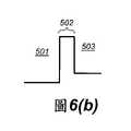
圖5為一示例之儲存電晶體的包含導帶邊界511及價帶邊界512的能帶圖,其具有通道區501、穿隧介電層502及電荷捕捉層503。FIG. 5 is an energy band diagram including a
圖6(a)-圖6(c)分別為(i)在儲存電晶體中基底501、穿隧介電層502及電荷捕捉層503的導帶之最低能階;(ii)在未施加一電壓下,儲存電晶體中前述層的導帶之最低能階;及(iii)當施加一抹除電壓時,基底501及電荷捕捉層503之間的電子能量偏移515。6(a)-FIG. 6(c) are respectively (i) the lowest energy level of the conduction band of the
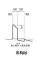
圖7(a)-圖7(c)分別為(i)在儲存電晶體之基底601、穿隧介電層602、低導帶台階之阻障介電603及電荷捕捉層604的相對導帶偏移;(ii)在未施加一電壓下,儲存電晶體中前述層的能帶圖;及(iii)當施加一抹除電壓時,基底601及電荷捕捉層604之間的電子能量偏移615。7(a) to 7(c) are respectively (i) the relative conduction bands of the
圖8(a)-8(c)描繪了圖7(a)-圖7(c)中介電層602-604的導帶台階參數。Figures 8(a)-8(c) depict conduction band step parameters for the dielectric layers 602-604 of Figures 7(a)-7(c).
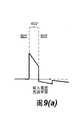
圖9(a)為圖7(a)之儲存電晶體中直接穿隧,以及圖9(b)及圖9(c)分別為圖7(b)-圖7(c)之儲存電晶體中MFN穿隧。FIG. 9(a) shows direct tunneling in the storage transistor of FIG. 7(a), and FIG. 9(b) and FIG. 9(c) show the storage transistors of FIGS. 7(b) to 7(c), respectively. MFN tunneling.
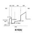
圖10(a)及10(b)為基於橫跨穿隧介電層602的一伏特壓降下寫入及抹除操作期間結構之能帶圖(也就是一寫入操作期間下b=1eV,以及一抹除操作期間下b'=1eV)。FIGS. 10(a) and 10(b) are energy band diagrams of structures during write and erase operations based on a one-volt voltage drop across the tunnel dielectric layer 602 (ie,b =1 during a write operation).eV , andb' =1eV during an erase operation).
圖11(a)-圖11(d)為本發明中儲存電晶體的各種模擬結果。FIG. 11(a)-FIG. 11(d) are various simulation results of the storage transistor in the present invention.
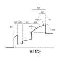
圖12(a)為一抹除操作期間一儲存電晶體中閘極堆疊之導帶的能帶圖。Figure 12(a) is an energy band diagram of the conduction band of the gate stack in a storage transistor during an erase operation.
圖12(b)為一抹除操作期間一儲存電晶體中閘極堆疊之導帶的能帶圖,根據本發明一實施例中儲存電晶體具有額外的氧化鋁層607於阻擋介電層610中。12(b) is an energy band diagram of the conduction band of the gate stack in a storage transistor having an additional
本發明利用一裝置結構,在一所需低能量範圍內(稱為「冷電子」),確保電子穿隧出一電荷捕捉層進入儲存電晶體之通道區(例如在一抹除操作期間),使得最後的電洞產生也都是低能量,因此對寫入視窗的損害減少,改善了儲存電晶體的持久度,以超過了1011寫入-抹除週期。裝置結構提供一大量直接穿隧寫入電流密度,其超過1.0amps/cm2(例如5.0amps/cm2)。本發明特別有利於使用在三維記憶結構中形成薄膜儲存電晶體之儲存層,例如前述說明由哈拉利所揭露在三維陣列之反或閘記憶串中的準揮發性儲存電晶體。The present invention utilizes a device structure in a desired low energy range (referred to as "cold electrons") to ensure that electrons tunnel out of a charge-trapping layer into the channel region of a storage transistor (eg, during an erase operation) such that The final hole generation is also low energy, so there is less damage to the write window, improving the endurance of the storage transistor to exceed 1011 write-erase cycles. The device structure provides a substantial direct tunneling write current density in excess of 1.0 amps/cm2 (eg, 5.0 amps/cm2 ). The present invention is particularly advantageous for use with storage layers that form thin film storage transistors in three-dimensional memory structures, such as the quasi-volatile storage transistors in three-dimensional array inverse or gate memory strings previously described by Harari.
本發明之一實施例由圖5之模型所描繪,其示出一示例之儲存電晶體的導帶邊界511及價帶邊界512,其具有通道區501、穿隧介電層502及電荷捕捉層503。如圖5所示,箭頭514表示電子直接由電荷捕捉層503穿隧至通道區501。電荷捕捉層503之導帶中最低能階與通道區501之導帶中最低能階之間的能量差(「導帶台階」(conduction band offset)),如符號515所指,是一電子穿隧所預期的能量損失。One embodiment of the present invention is depicted by the model of Figure 5, which shows the
本發明藉著嚴選一穿隧介電材料及一電荷捕捉介電材料的組合材料,以獲得相對於儲存電晶體之半導體基底(也就是通道區)在這些層所需的導帶台階。圖6(a)為在儲存電晶體中基底501、穿隧介電層502及電荷捕捉層503的導帶之最低能階。圖6(b)為在未施加一電壓下,儲存電晶體中前述層的導帶之最低能階。圖6(c)為當施加一抹除電壓時,基底501及電荷捕捉層503之間的電子能量偏移515。電子能量偏移515取決於基底501及穿隧介電層502及電荷捕捉層中503中每一個之間的導帶台階,以及取決於抹除操作所施加的電壓。如圖6(c)所示,對於穿隧介電層502而言,使用不同的電荷捕捉材料作為電荷捕捉層503,具有相對於基底層501不同的導帶台階,造成到達基底501之穿隧電子的能量損失更大或更小。同樣地,對於電荷捕捉層503而言,使用不同的穿隧介電材料作為穿隧介電層502,具有相對於基底層501不同的導帶台階,也造成了到達基底501之穿隧電子的能量損失更大或更小。The present invention obtains the required conduction band steps in these layers relative to the semiconductor substrate (ie, the channel region) of the storage transistor by carefully selecting a combination of a tunneling dielectric material and a charge-trapping dielectric material. FIG. 6( a ) shows the lowest energy levels of the conduction bands of the
穿隧介電層501可以薄至5-40埃(Å),且可由氧化矽(例如SiO2)、氮化矽(SiN)或氮氧化矽(SiON)所形成。氧化矽穿隧介電層可以利用常規氧化技術(例如一高溫氧化)、化學合成(例如原子層積ALD)或任何前述技術的適當組合來形成。一活性氧(O2)製程可包含一臭氧步驟(例如使用脈衝臭氧(pulsed ozone)),用於精確控制厚度以及改善氧化物質量(例如減少由於缺陷部位的洩漏)。臭氧步驟以保形方式增強了氧化物的固化,這對於三維電晶體結構特別有利。一退火步驟(例如一氫氣(H2)退火、一氨氣(NH3)退火或一快速熱退火)也可以強化穿隧介電層501。氮化矽穿隧介電層可以利用常規氮化、直接合成、化學合成(例如原子層積ALD)或任何前述技術的適當組合來形成。電漿製程可用於精確控制厚度以及改善介電質量(例如減少由於缺陷部位的洩漏)。The
穿隧介電層501也可包含額外的一薄氧化鋁(Al2O3)層(例如10Å或更薄)。在穿隧介電層中額外的氧化鋁層可以在非晶相(amorphous phase)中合成,以減少由於缺陷部位所造成的洩漏。Tunneling
以下材料可以用於提供穿隧介電層502及電荷捕捉層503:

在電荷捕捉層中使用一低導帶台階可有效增加穿隧介電層中的穿隧能障,從而改善資料保存能力。Using a low conduction band step in the charge trapping layer can effectively increase the tunneling energy barrier in the tunneling dielectric layer, thereby improving data retention.
替代地,可以將低導帶台階之一阻障材料引入至儲存電晶體中穿隧介電層及電荷捕捉層之間。圖7(a)-圖7(c)為此結構的能帶圖。圖7(a)為在儲存電晶體之基底601、穿隧介電層602、低導帶台階之阻障介電603及電荷捕捉層604的相對導帶偏移。圖7(b)為在未施加一電壓下,儲存電晶體中前述層的能帶圖。圖7(c)為當施加一抹除電壓時,基底601及電荷捕捉層604之間的電子能量偏移615。電子能量偏移615取決於基底601及穿隧介電層602、低導帶台階之阻障介電603及電荷捕捉層604中每一個之間的導帶台階,以及取決於抹除操作所施加的電壓。如圖7(a)-圖7(c)所示,低導帶台階(LCBO)之阻障介電603最好具有相對基底601皆小於穿隧介電層602及電荷捕捉層604之導帶台階的一導電台階。嚴選穿隧介電層602、低導帶台階之阻障介電603及電荷捕捉層604的材料,無論是寫入或抹除操作,皆可實現冷電子直接穿隧,以令儲存電晶體具有高持久度。Alternatively, a barrier material of a low conduction band step can be introduced into the storage transistor between the tunneling dielectric layer and the charge trapping layer. Figures 7(a)-7(c) are energy band diagrams for this structure. FIG. 7( a ) shows the relative conduction band offsets of the
圖8(a)-8(c)描繪了圖7(a)-圖7(c)中介電層602-604的導帶台階參數。如圖8(a)所示,(i)參數B表示穿隧介電層602相對於基底601的導電台階,(ii)參數a表示LCBO阻障層603之導帶台階相對於穿隧介電層602的導帶台階,(iii)參數d表示LCBO阻障層603相對於基底601的導電台階,以及(iv)參數c表示電荷捕捉層604相對於基底601的導電台階。根據本發明之一實施例,LCBO阻障層603之導電台階應該不大於電荷捕捉層604之導電台階(也就是d
圖8(b)示出由於寫入電壓而在穿隧介電層602之導帶底部傾斜了能階。通過穿隧介電層602之厚度,傾斜(the sloping)使穿隧介電層602之能階降低參數b。為了通過直接穿隧實現寫入操作,參數b應該大於或等於參數c的值(也就是b
當穿隧介電層602之電壓降小於電荷捕捉層604之導電台階(也就是b<c),由於至少一部分的LCBO阻障層603保持一穿隧阻障,穿隧阻障會變寬。在那種情況下,直接穿隧可被改進的福勒-諾德漢(modified Fowler-Nordheim,MFN)機制取代,以提供一相對直接穿隧小得多的電流(例如小於0.1amps/cm2)。When the voltage drop of the
在圖7(a)-圖7(c)之儲存電晶體中,圖9(a)為一寫入電壓的施加下的直接穿隧,圖9(b)及圖9(c)分別為一低電壓(中間電壓)及一更低電壓下MFN穿隧。可以認識到在儲存電晶體的操作期間,MFN穿隧可能發生在低電壓干擾的區域中。不過,對於具有圖7(a)-圖7(c)所描繪之結構的儲存電晶體,所施加的電壓範圍下,這樣的MFN穿隧電流可以非常低。選擇用於電荷捕捉層604及阻障層603的材料及厚度,使得讀取干擾電壓(read disturb voltages)、寫入禁止電壓(programming inhibit voltages)或抹除禁止電壓(erase inhibit voltages)落入了限制穿隧至MFN機制的低電壓或中間電壓之範圍內。In the storage transistor shown in FIG. 7(a)-FIG. 7(c), FIG. 9(a) is the direct tunneling under the application of a write voltage, and FIG. 9(b) and FIG. 9(c) are respectively a MFN tunneling at low voltage (intermediate voltage) and a lower voltage. It is recognized that MFN tunneling may occur in regions of low voltage disturbance during operation of the storage transistor. However, for storage transistors having the structures depicted in Figures 7(a)-7(c), such MFN tunneling currents can be very low over the applied voltage range. The materials and thicknesses for
如此,本發明中儲存電晶體具有一重要優點:在寫入電壓下由於直接穿隧具有高電流,而當處在一低電壓下僅有低MFN穿隧電流。這種特性減少了讀取、寫入禁止或抹除禁止操作下的干擾,且改善了資料保存性及耐久性,特別是利用直接穿隧以快速寫入及抹除操作的本發明之準揮發性儲存電晶體。關於此點,由於通道區中產生的電洞為低能量,LCBO阻障層603藉著允許冷電子抹除操作來改善耐久性,減少了裝置劣化。Thus, the storage transistor of the present invention has an important advantage: under the write voltageSince direct tunneling has high current, there is only low MFN tunneling current at a low voltage. This feature reduces interference under read, write inhibit or erase inhibit operations and improves data retention and durability, especially the quasi-volatile of the present invention utilizing direct tunneling for fast write and erase operations Sexual storage transistors. In this regard, the
由於讀取干擾、寫入禁止干擾或抹除禁止干擾均在一低電壓下發生,藉著在一低電壓限制穿隧至MFN穿隧,LCBO阻障層603也改善了資料保存性及耐久性以及減少了讀取干擾、寫入禁止干擾或抹除禁止干擾。舉例來說,寫入禁止干擾或抹除禁止干擾發生在半選擇(half-select)或一低於分別使用於寫入及抹除操作下的電壓。所有優點皆在儲存電晶體偏壓於低電壓時體現,而同時維持了在儲存電晶體偏壓於較高讀取、寫入或抹除電壓下直接穿隧之高效率的優點。The
圖8(c)示出一抹除操作期間下穿隧介電層602之導帶底部的傾斜能階。通過穿隧介電層602之厚度,傾斜(the sloping)使穿隧介電層602之能階提高了參數b’。在抹除操作期間,電子由電荷捕捉層604直接穿隧至基底601損失一由參數A表示的能量,其中參數A之關係為A=b'-c。注意得是,電荷捕捉層604之導帶台階應該比電荷捕捉點之能階的量和該能階之導帶之差還要大,以令位在電荷捕捉點的電子可以成為直接穿隧電流。FIG. 8( c ) shows the sloped energy levels at the bottom of the conduction band of the lower
根據本發明之一實施例,基底601可以由一P摻雜矽實現,穿隧介電層602可由1奈米厚的二氧化矽層(B=3.15eV)實現,低導電台階之阻障層603可由2奈米厚的二氧化鈦層(d=0.3eV)實現,電荷捕捉層604可由4奈米厚的富矽之氮化矽(也就是SiN:Si,c=1.35eV)實現,以及另一4奈米厚的二氧化矽層可作為阻擋介電層。閘電極606可由一高摻雜P型多晶矽來實現。圖10(a)及10(b)為基於橫跨穿隧介電層602的一伏特壓降下寫入及抹除操作期間結構之能帶圖(也就是一寫入操作期間下b=1eV,以及一抹除操作期間下b'=1eV)。如圖10(b)中箭頭1001所示,在抹除操作期間,一電子通過直接穿隧到達基底601損失了大約1.4電子伏特的能量。在LCBO阻障層603中分散,如箭頭1002所指,可更加減少這些能量損失。According to an embodiment of the present invention, the
根據本發明之另一實施例,基底601可以由P摻雜矽實現,穿隧介電層602可由1奈米厚的二氧化矽層(B=3.15eV)實現,低導電台階之阻障層603可由2奈米厚的二氧化鈰層(d=0.6eV),電荷捕捉層604可由4奈米厚的富矽之氮化矽(Si3N4:Si,c=1.35eV),以及另一5奈米厚的二氧化矽層可作為阻擋介電層。閘電極606可由一高摻雜P型多晶矽來實現。According to another embodiment of the present invention, the
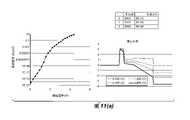
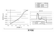
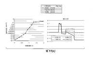
圖11(a)-圖11(d)為本發明中儲存電晶體的各種模擬結果。FIG. 11(a)-FIG. 11(d) are various simulation results of the storage transistor in the present invention.
圖11(a)為一儲存電晶體之模擬圖,其具有0.8奈米厚的二氧化矽之穿隧介電層、2.0奈米厚的二氧化鋯之LCBO阻障層及5奈米厚的富矽之氮化矽的捕捉層。圖11(a)呈現在3.1伏特左右的寫入電壓下,可實現超過1.0amps/cm2之直接穿隧電流密度。Figure 11(a) is a simulation of a storage transistor with a 0.8 nm thick silicon dioxide tunneling dielectric layer, a 2.0 nm thick zirconia LCBO barrier layer, and a 5 nm thick Capture layer of silicon-rich silicon nitride. Figure 11(a) shows that at write voltages around 3.1 volts, direct tunneling current densities in excess of 1.0 amps/cm2 can be achieved.
圖11(b)為一儲存電晶體之模擬圖,其具有1.0奈米厚的二氧化矽之穿隧介電層、2.0奈米厚的二氧化鈰之LCBO阻障層及4.0奈米厚的富矽之氮化矽的捕捉層。圖11(b)呈現在1.6伏特左右的寫入電壓下,可實現超過1.0amps/cm2之直接穿隧電流密度。Figure 11(b) is a simulation of a storage transistor with a 1.0 nm thick silicon dioxide tunneling dielectric layer, a 2.0 nm thick LCBO barrier layer of ceria, and a 4.0 nm thick Capture layer of silicon-rich silicon nitride. Figure 11(b) shows that at write voltages around 1.6 volts, direct tunneling current densities in excess of 1.0 amps/cm2 can be achieved.
圖11(c)為一儲存電晶體之模擬圖,其具有1.0奈米厚的二氧化矽之穿隧介電層、2.0奈米厚的五氧化二鉭之LCBO阻障層及4.0奈米厚的富矽之氮化矽的捕捉層。圖11(c)呈現在1.8伏特左右的寫入電壓下,可實現超過1.0amps/cm2之直接穿隧電流密度。Figure 11(c) is a simulation of a storage transistor with a 1.0 nm thick tunneling dielectric layer of silicon dioxide, a 2.0 nm thick LCBO barrier layer of tantalum pentoxide, and a 4.0 nm thick layer the trapping layer of silicon-rich silicon nitride. Figure 11(c) shows that at write voltages around 1.8 volts, direct tunneling current densities in excess of 1.0 amps/cm2 can be achieved.
圖11(d)為一儲存電晶體之模擬圖,其具有1.0奈米厚的氮化矽之穿隧介電層、2.0奈米厚的二氧化鈰之LCBO阻障層及4.0奈米厚的富矽之氮化矽的捕捉層。圖11(d)呈現在2.1伏特左右的寫入電壓下,可實現超過1.0amps/cm2之直接穿隧電流密度。Figure 11(d) is a simulation of a storage transistor with a 1.0 nm thick tunneling dielectric layer of silicon nitride, a 2.0 nm thick LCBO barrier layer of ceria, and a 4.0 nm thick Capture layer of silicon-rich silicon nitride. Figure 11(d) shows that at write voltages around 2.1 volts, direct tunneling current densities in excess of 1.0 amps/cm2 can be achieved.
圖12(a)描繪在抹除操作期間可能發生一「反向注入電子(reverse injection electrons)」現象。反向注入的電子可能對於耐久性產生不利影響。圖12(a)為抹除操作期間一儲存電晶體中閘極堆疊之導帶的能帶圖。如圖12(a)所示,閘極堆疊包含基底601、穿隧介電602、LCBO阻障介電603、電荷捕捉層604、阻擋介電層605及閘電極606。(阻擋介電層605可以例如為二氧化矽(SiO2))。於一抹除操作期間,橫跨阻擋介電層605相對高的電場可能導致高能量的電子,如圖12(a)中箭頭1201所指,由閘電極穿隧至電荷捕捉層604,或甚至進入穿隧介電層602。這些反向注入的電子可能損害這些層,而對儲存電晶體的耐久性產生不利影響。Figure 12(a) depicts a "reverse injection electrons" phenomenon that may occur during an erase operation. Back-injected electrons may adversely affect durability. Figure 12(a) is an energy band diagram of the conduction band of the gate stack in a storage transistor during an erase operation. As shown in FIG. 12( a ), the gate stack includes a
根據本發明之一實施例,藉著包含具有高介電常數(高k材料)的材料層,例如在阻擋介電層(如圖10(a)中的阻擋介電層606)中的氧化鋁(Al2O3),可以顯著減少或基本上消除反向注入電子。在此實施例中,閘電極可以使用一高功函數金屬(例如高於3.8eV,優選不小於4.0eV)。高k材料的tH提供一等效氧化物厚度tEOT為:
圖12(b)為一抹除操作期間一儲存電晶體中閘極堆疊之導帶的能帶圖,根據本發明一實施例,儲存電晶體具有額外的氧化鋁層607於阻擋介電層610中。在圖12(b)中,阻擋介電層610包含氧化鋁層607及二氧化矽層608。在一實際態樣中,阻擋介電層610的等效氧化物厚度基本上與圖12(a)中阻擋介電層605相同。然而,由於氧化鋁的相對介電常數為9.0,而二氧化矽的相對介電常數為3.9,因此圖12(b)中氧化鋁607及二氧化矽608的實際組合物理厚度大於圖12(a)中阻擋介電層605的厚度。由於高k介電層607之相對介電常數大於二氧化矽層608之相對介電常數,高k介電層607中的電場低於二氧化矽層608中的電場。圖12(b)中阻擋介電層610之較大的組合物理厚度(於閘電極606及電荷捕捉層604之間提供了一較寬的穿隧阻障),以及在閘電極606與高k材料607之間介面的一較低的電場,減少了或消除反向電子注入,從而達到一改善的耐久性。配合高k電性層607(例如氧化鋁),優選高功函數金屬作為閘電極。高功函數金屬在閘電極-氧化鋁介面處產生一高阻障(如圖12(b)中阻障高度1202所指),顯著減少了反向電子注入的抹除操作。合適的高功函數金屬包含:鎢(w)、氮化鉭(TaN)及氮化鉭矽(TaSiN)。Figure 12(b) is an energy band diagram of the conduction band of the gate stack in a storage transistor having an additional
以上詳細描述提供說明本發明的特定實施例,但並不以此為限。本發明範圍內的各種修改和變化都是可能的。以下申請權利範圍闡述了本發明。The foregoing detailed description is provided to illustrate specific embodiments of the invention, but not to be limiting. Various modifications and changes are possible within the scope of the present invention. The following claims set forth the invention.
501:通道區501: Passage Area
502:穿隧介電層502: Tunneling Dielectric Layer
503:電荷捕捉層503: charge trapping layer
511:導帶邊界511: Conduction Band Boundary
512:價帶邊界512: Valence Band Boundary
514:箭頭514: Arrow
515、516:電子能量偏移515, 516: Electron energy offset
Claims (34)
Translated fromChineseApplications Claiming Priority (4)
| Application Number | Priority Date | Filing Date | Title |
|---|---|---|---|
| US202062964472P | 2020-01-22 | 2020-01-22 | |
| US62/964,472 | 2020-01-22 | ||
| US202062992754P | 2020-03-20 | 2020-03-20 | |
| US62/992,754 | 2020-03-20 |
Publications (2)
| Publication Number | Publication Date |
|---|---|
| TW202143446A TW202143446A (en) | 2021-11-16 |
| TWI767512Btrue TWI767512B (en) | 2022-06-11 |
Family
ID=76857256
Family Applications (1)
| Application Number | Title | Priority Date | Filing Date |
|---|---|---|---|
| TW110101376ATWI767512B (en) | 2020-01-22 | 2021-01-14 | Cool electron erasing in thin-film storage transistors |
Country Status (4)
| Country | Link |
|---|---|
| US (2) | US11515432B2 (en) |
| CN (1) | CN114846551A (en) |
| TW (1) | TWI767512B (en) |
| WO (1) | WO2021150879A1 (en) |
Families Citing this family (2)
| Publication number | Priority date | Publication date | Assignee | Title |
|---|---|---|---|---|
| KR102719982B1 (en)* | 2017-06-20 | 2024-10-22 | 선라이즈 메모리 코포레이션 | 3D NOR memory array architecture and its manufacturing method |
| US11984513B2 (en)* | 2020-10-14 | 2024-05-14 | Korea Advanced Institute Of Science And Technology | Charge trapping non-volatile organic memory device |
Citations (2)
| Publication number | Priority date | Publication date | Assignee | Title |
|---|---|---|---|---|
| US20080054346A1 (en)* | 2006-09-01 | 2008-03-06 | Kabushiki Kaisha Toshiba | Semiconductor device |
| TW201601258A (en)* | 2014-06-19 | 2016-01-01 | 旺宏電子股份有限公司 | Band gap engineering memory having a plurality of charge storage layers for storing charges |
Family Cites Families (266)
| Publication number | Priority date | Publication date | Assignee | Title |
|---|---|---|---|---|
| US4213139A (en) | 1978-05-18 | 1980-07-15 | Texas Instruments Incorporated | Double level polysilicon series transistor cell |
| JP2643833B2 (en)* | 1994-05-30 | 1997-08-20 | 日本電気株式会社 | Semiconductor memory device and method of manufacturing the same |
| US5583808A (en) | 1994-09-16 | 1996-12-10 | National Semiconductor Corporation | EPROM array segmented for high performance and method for controlling same |
| US5646886A (en) | 1995-05-24 | 1997-07-08 | National Semiconductor Corporation | Flash memory having segmented array for improved operation |
| JPH098290A (en) | 1995-06-20 | 1997-01-10 | Mitsubishi Electric Corp | Semiconductor device and manufacture thereof |
| US5789776A (en) | 1995-09-22 | 1998-08-04 | Nvx Corporation | Single poly memory cell and array |
| US5768192A (en) | 1996-07-23 | 1998-06-16 | Saifun Semiconductors, Ltd. | Non-volatile semiconductor memory cell utilizing asymmetrical charge trapping |
| EP0833348B1 (en) | 1996-09-30 | 2003-07-09 | STMicroelectronics S.r.l. | Method and circuit for checking multilevel programming of floating-gate nonvolatile memory cells, particlarly flash cells |
| US5915167A (en) | 1997-04-04 | 1999-06-22 | Elm Technology Corporation | Three dimensional structure memory |
| KR100242723B1 (en) | 1997-08-12 | 2000-02-01 | 윤종용 | Cell array structure of non-volatile semiconductor memory device and method for manufacturing thereof |
| US6350704B1 (en) | 1997-10-14 | 2002-02-26 | Micron Technology Inc. | Porous silicon oxycarbide integrated circuit insulator |
| US6040605A (en) | 1998-01-28 | 2000-03-21 | Hitachi, Ltd. | Semiconductor memory device |
| US6107133A (en) | 1998-05-28 | 2000-08-22 | International Business Machines Corporation | Method for making a five square vertical DRAM cell |
| JP2000200842A (en) | 1998-11-04 | 2000-07-18 | Sony Corp | Nonvolatile semiconductor memory device, manufacturing method and writing method |
| US6118171A (en) | 1998-12-21 | 2000-09-12 | Motorola, Inc. | Semiconductor device having a pedestal structure and method of making |
| JP2000285016A (en) | 1999-03-30 | 2000-10-13 | Sanyo Electric Co Ltd | Memory control circuit |
| JP4899241B2 (en) | 1999-12-06 | 2012-03-21 | ソニー株式会社 | Nonvolatile semiconductor memory device and operation method thereof |
| TW587252B (en) | 2000-01-18 | 2004-05-11 | Hitachi Ltd | Semiconductor memory device and data processing device |
| US6407435B1 (en) | 2000-02-11 | 2002-06-18 | Sharp Laboratories Of America, Inc. | Multilayer dielectric stack and method |
| US6639835B2 (en) | 2000-02-29 | 2003-10-28 | Micron Technology, Inc. | Static NVRAM with ultra thin tunnel oxides |
| US6362508B1 (en) | 2000-04-03 | 2002-03-26 | Tower Semiconductor Ltd. | Triple layer pre-metal dielectric structure for CMOS memory devices |
| JP2001357682A (en) | 2000-06-12 | 2001-12-26 | Sony Corp | Memory system, and its programming method |
| KR100821456B1 (en) | 2000-08-14 | 2008-04-11 | 샌디스크 쓰리디 엘엘씨 | Dense array and charge storage device and manufacturing method thereof |
| US6580124B1 (en) | 2000-08-14 | 2003-06-17 | Matrix Semiconductor Inc. | Multigate semiconductor device with vertical channel current and method of fabrication |
| US6621725B2 (en) | 2000-08-17 | 2003-09-16 | Kabushiki Kaisha Toshiba | Semiconductor memory device with floating storage bulk region and method of manufacturing the same |
| US20020193484A1 (en) | 2001-02-02 | 2002-12-19 | The 54 Group, Ltd. | Polymeric resins impregnated with insect repellants |
| US6531727B2 (en) | 2001-02-09 | 2003-03-11 | Micron Technology, Inc. | Open bit line DRAM with ultra thin body transistors |
| US6744094B2 (en) | 2001-08-24 | 2004-06-01 | Micron Technology Inc. | Floating gate transistor with horizontal gate layers stacked next to vertical body |
| US7012297B2 (en) | 2001-08-30 | 2006-03-14 | Micron Technology, Inc. | Scalable flash/NV structures and devices with extended endurance |
| GB0123416D0 (en) | 2001-09-28 | 2001-11-21 | Memquest Ltd | Non-volatile memory control |
| US6873004B1 (en) | 2002-02-04 | 2005-03-29 | Nexflash Technologies, Inc. | Virtual ground single transistor memory cell, memory array incorporating same, and method of operation thereof |
| US7365403B1 (en)* | 2002-02-13 | 2008-04-29 | Cypress Semiconductor Corp. | Semiconductor topography including a thin oxide-nitride stack and method for making the same |
| US7064018B2 (en) | 2002-07-08 | 2006-06-20 | Viciciv Technology | Methods for fabricating three dimensional integrated circuits |
| US6774458B2 (en) | 2002-07-23 | 2004-08-10 | Hewlett Packard Development Company, L.P. | Vertical interconnection structure and methods |
| JP2004079606A (en) | 2002-08-12 | 2004-03-11 | Fujitsu Ltd | Semiconductor device having high dielectric constant film and method of manufacturing the same |
| US7005350B2 (en) | 2002-12-31 | 2006-02-28 | Matrix Semiconductor, Inc. | Method for fabricating programmable memory array structures incorporating series-connected transistor strings |
| KR100881201B1 (en) | 2003-01-09 | 2009-02-05 | 삼성전자주식회사 | Sonos memory device having a side gate and its manufacturing method |
| US7307308B2 (en) | 2003-04-07 | 2007-12-11 | Silicon Storage Technology, Inc. | Buried bit line non-volatile floating gate memory cell with independent controllable control gate in a trench, and array thereof, and method of formation |
| US6754105B1 (en) | 2003-05-06 | 2004-06-22 | Advanced Micro Devices, Inc. | Trench side wall charge trapping dielectric flash memory device |
| JP4108537B2 (en) | 2003-05-28 | 2008-06-25 | 富士雄 舛岡 | Semiconductor device |
| KR100546331B1 (en) | 2003-06-03 | 2006-01-26 | 삼성전자주식회사 | Multi-port memory device operates independently for each stack bank |
| US20040262772A1 (en) | 2003-06-30 | 2004-12-30 | Shriram Ramanathan | Methods for bonding wafers using a metal interlayer |
| KR100535651B1 (en) | 2003-06-30 | 2005-12-08 | 주식회사 하이닉스반도체 | Method for reading a flash memory cell and a flash memory equipment of NAND and NOR type |
| JP4545423B2 (en) | 2003-12-09 | 2010-09-15 | ルネサスエレクトロニクス株式会社 | Semiconductor device |
| US7241654B2 (en) | 2003-12-17 | 2007-07-10 | Micron Technology, Inc. | Vertical NROM NAND flash memory array |
| US7223653B2 (en) | 2004-06-15 | 2007-05-29 | International Business Machines Corporation | Process for forming a buried plate |
| US7378702B2 (en) | 2004-06-21 | 2008-05-27 | Sang-Yun Lee | Vertical memory device structures |
| JP4785180B2 (en) | 2004-09-10 | 2011-10-05 | 富士通セミコンダクター株式会社 | Ferroelectric memory, multilevel data recording method, and multilevel data reading method |
| JP4284259B2 (en) | 2004-09-28 | 2009-06-24 | シャープ株式会社 | Semiconductor memory device and electronic device |
| US7412560B2 (en) | 2004-12-16 | 2008-08-12 | Sandisk Corporation | Non-volatile memory and method with multi-stream updating |
| US7366826B2 (en) | 2004-12-16 | 2008-04-29 | Sandisk Corporation | Non-volatile memory and method with multi-stream update tracking |
| US7473589B2 (en) | 2005-12-09 | 2009-01-06 | Macronix International Co., Ltd. | Stacked thin film transistor, non-volatile memory devices and methods for fabricating the same |
| US7374964B2 (en)* | 2005-02-10 | 2008-05-20 | Micron Technology, Inc. | Atomic layer deposition of CeO2/Al2O3 films as gate dielectrics |
| US7498247B2 (en)* | 2005-02-23 | 2009-03-03 | Micron Technology, Inc. | Atomic layer deposition of Hf3N4/HfO2 films as gate dielectrics |
| US8314024B2 (en) | 2008-12-19 | 2012-11-20 | Unity Semiconductor Corporation | Device fabrication |
| KR100673105B1 (en) | 2005-03-31 | 2007-01-22 | 주식회사 하이닉스반도체 | Vertical transistors in semiconductor devices and methods of forming them |
| US7612403B2 (en)* | 2005-05-17 | 2009-11-03 | Micron Technology, Inc. | Low power non-volatile memory and gate stack |
| US7402850B2 (en)* | 2005-06-21 | 2008-07-22 | Micron Technology, Inc. | Back-side trapped non-volatile memory device |
| KR101377305B1 (en) | 2005-06-24 | 2014-03-25 | 구글 인코포레이티드 | An integrated memory core and memory interface circuit |
| US7538000B2 (en) | 2005-07-28 | 2009-05-26 | Freescale Semiconductor, Inc. | Method of forming double gate transistors having varying gate dielectric thicknesses |
| US7612411B2 (en) | 2005-08-03 | 2009-11-03 | Walker Andrew J | Dual-gate device and method |
| US7429767B2 (en)* | 2005-09-01 | 2008-09-30 | Micron Technology, Inc. | High performance multi-level non-volatile memory device |
| KR101293365B1 (en) | 2005-09-30 | 2013-08-05 | 모사이드 테크놀로지스 인코퍼레이티드 | Memory with output control |
| US20080012065A1 (en)* | 2006-07-11 | 2008-01-17 | Sandisk Corporation | Bandgap engineered charge storage layer for 3D TFT |
| US7727908B2 (en)* | 2006-08-03 | 2010-06-01 | Micron Technology, Inc. | Deposition of ZrA1ON films |
| KR100834396B1 (en) | 2006-12-27 | 2008-06-04 | 주식회사 하이닉스반도체 | Pattern formation method of semiconductor device |
| US7857907B2 (en) | 2007-01-25 | 2010-12-28 | Au Optronics Corporation | Methods of forming silicon nanocrystals by laser annealing |
| US7898009B2 (en) | 2007-02-22 | 2011-03-01 | American Semiconductor, Inc. | Independently-double-gated transistor memory (IDGM) |
| JP2008251138A (en) | 2007-03-30 | 2008-10-16 | Toshiba Corp | Nonvolatile semiconductor memory, control method of nonvolatile semiconductor memory, nonvolatile semiconductor memory system, and memory card |
| US7512012B2 (en) | 2007-04-30 | 2009-03-31 | Macronix International Co., Ltd. | Non-volatile memory and manufacturing method and operating method thereof and circuit system including the non-volatile memory |
| US7687891B2 (en) | 2007-05-14 | 2010-03-30 | Infineon Technologies Ag | Diode having one or more zones of a first conductivity type and one or more zones of a second conductivity type each located within a layer of the second conductivity type |
| US20080291723A1 (en) | 2007-05-23 | 2008-11-27 | Wang Daniel C | Source biasing of nor-type flash array with dynamically variable source resistance |
| US8871595B2 (en) | 2007-05-25 | 2014-10-28 | Cypress Semiconductor Corporation | Integration of non-volatile charge trap memory devices and logic CMOS devices |
| US20090179253A1 (en) | 2007-05-25 | 2009-07-16 | Cypress Semiconductor Corporation | Oxide-nitride-oxide stack having multiple oxynitride layers |
| JP5130596B2 (en) | 2007-05-30 | 2013-01-30 | 国立大学法人東北大学 | Semiconductor device |
| DE102007035251B3 (en) | 2007-07-27 | 2008-08-28 | X-Fab Semiconductor Foundries Ag | Isolation ditches with different side panel doping production method for use in dig-insulating smart-power-technology for leading connection of buried endowed layers, comprises drilling narrow and broad ditch by photolithographic process |
| US7816727B2 (en) | 2007-08-27 | 2010-10-19 | Macronix International Co., Ltd. | High-κ capped blocking dielectric bandgap engineered SONOS and MONOS |
| US7709359B2 (en) | 2007-09-05 | 2010-05-04 | Qimonda Ag | Integrated circuit with dielectric layer |
| US20090140318A1 (en)* | 2007-12-03 | 2009-06-04 | Zhong Dong | Nonvolatile memories with higher conduction-band edge adjacent to charge-trapping dielectric |
| US20090157946A1 (en) | 2007-12-12 | 2009-06-18 | Siamak Arya | Memory having improved read capability |
| US7542348B1 (en) | 2007-12-19 | 2009-06-02 | Juhan Kim | NOR flash memory including bipolar segment read circuit |
| US7898857B2 (en) | 2008-03-20 | 2011-03-01 | Micron Technology, Inc. | Memory structure having volatile and non-volatile memory portions |
| JP5354944B2 (en) | 2008-03-27 | 2013-11-27 | 株式会社東芝 | Semiconductor device and field effect transistor |
| US8304823B2 (en) | 2008-04-21 | 2012-11-06 | Namlab Ggmbh | Integrated circuit including a ferroelectric memory cell and method of manufacturing the same |
| US8072811B2 (en) | 2008-05-07 | 2011-12-06 | Aplus Flash Technology, Inc, | NAND based NMOS NOR flash memory cell, a NAND based NMOS NOR flash memory array, and a method of forming a NAND based NMOS NOR flash memory array |
| US9123422B2 (en)* | 2012-07-02 | 2015-09-01 | Super Talent Technology, Corp. | Endurance and retention flash controller with programmable binary-levels-per-cell bits identifying pages or blocks as having triple, multi, or single-level flash-memory cells |
| US8289775B2 (en) | 2008-06-20 | 2012-10-16 | Aplus Flash Technology, Inc. | Apparatus and method for inhibiting excess leakage current in unselected nonvolatile memory cells in an array |
| KR101435588B1 (en) | 2008-06-23 | 2014-09-25 | 삼성전자주식회사 | Nonvolatile memory device and manufacturing method thereof |
| KR101468594B1 (en) | 2008-07-31 | 2014-12-04 | 삼성전자주식회사 | Oxide semiconductor and thin film transistor including the same |
| JP5459650B2 (en)* | 2008-09-22 | 2014-04-02 | 株式会社東芝 | Memory cell of nonvolatile semiconductor memory device |
| US20100121994A1 (en) | 2008-11-10 | 2010-05-13 | International Business Machines Corporation | Stacked memory array |
| JP2010118580A (en) | 2008-11-14 | 2010-05-27 | Toshiba Corp | Non-volatile semiconductor memory device |
| US8148763B2 (en) | 2008-11-25 | 2012-04-03 | Samsung Electronics Co., Ltd. | Three-dimensional semiconductor devices |
| WO2010077414A1 (en) | 2008-12-09 | 2010-07-08 | Rambus Inc. | Non-volatile memory device for concurrent and pipelined memory operations |
| JP4956598B2 (en) | 2009-02-27 | 2012-06-20 | シャープ株式会社 | Nonvolatile semiconductor memory device and manufacturing method thereof |
| US8178396B2 (en) | 2009-03-11 | 2012-05-15 | Micron Technology, Inc. | Methods for forming three-dimensional memory devices, and related structures |
| US8284601B2 (en) | 2009-04-01 | 2012-10-09 | Samsung Electronics Co., Ltd. | Semiconductor memory device comprising three-dimensional memory cell array |
| JP2010251572A (en) | 2009-04-16 | 2010-11-04 | Toshiba Corp | Nonvolatile semiconductor memory device |
| US8139418B2 (en) | 2009-04-27 | 2012-03-20 | Micron Technology, Inc. | Techniques for controlling a direct injection semiconductor memory device |
| KR101635504B1 (en) | 2009-06-19 | 2016-07-04 | 삼성전자주식회사 | Program method of non-volatile memory device with three-dimentional vertical channel structure |
| KR101476817B1 (en) | 2009-07-03 | 2014-12-26 | 가부시키가이샤 한도오따이 에네루기 켄큐쇼 | Display device including transistor and manufacturing method thereof |
| JP2011028540A (en) | 2009-07-27 | 2011-02-10 | Renesas Electronics Corp | Information processing system, method for controlling cache memory, program and compiler |
| KR20110018753A (en) | 2009-08-18 | 2011-02-24 | 삼성전자주식회사 | Nonvolatile Memory Device, Its Program Method, And Memory System Including It |
| US8169835B2 (en) | 2009-09-28 | 2012-05-01 | Macronix International Co., Ltd. | Charge trapping memory cell having bandgap engineered tunneling structure with oxynitride isolation layer |
| KR101584113B1 (en) | 2009-09-29 | 2016-01-13 | 삼성전자주식회사 | Three-dimensional semiconductor memory device and manufacturing method thereof |
| JP5031809B2 (en) | 2009-11-13 | 2012-09-26 | ユニサンティス エレクトロニクス シンガポール プライベート リミテッド | Semiconductor device |
| EP2333830B1 (en) | 2009-12-07 | 2014-09-03 | STMicroelectronics (Research & Development) Limited | a package comprising a first and a second die coupled by a multiplexed bus |
| US8247895B2 (en) | 2010-01-08 | 2012-08-21 | International Business Machines Corporation | 4D device process and structure |
| JP2010108522A (en) | 2010-02-02 | 2010-05-13 | Toshiba Corp | Method of controlling memory system |
| US8026521B1 (en) | 2010-10-11 | 2011-09-27 | Monolithic 3D Inc. | Semiconductor device and structure |
| US8395942B2 (en) | 2010-05-17 | 2013-03-12 | Sandisk Technologies Inc. | Junctionless TFT NAND flash memory |
| KR101660432B1 (en) | 2010-06-07 | 2016-09-27 | 삼성전자 주식회사 | Semiconductor memory device having vertical structure |
| US10217667B2 (en) | 2011-06-28 | 2019-02-26 | Monolithic 3D Inc. | 3D semiconductor device, fabrication method and system |
| US20120063223A1 (en) | 2010-09-09 | 2012-03-15 | Aplus Flash Technology, Inc. | Most compact flotox-based combo NVM design without sacrificing EEPROM endurance cycles for 1-die data and code storage |
| US8630114B2 (en) | 2011-01-19 | 2014-01-14 | Macronix International Co., Ltd. | Memory architecture of 3D NOR array |
| KR20120085591A (en) | 2011-01-24 | 2012-08-01 | 김진선 | Non-volatile memory device, method of operating the same, and method of fabricating the same |
| KR20120085603A (en) | 2011-01-24 | 2012-08-01 | 김진선 | Non-volatile memory device, method of operating the same, and method of fabricating the same |
| ITTO20110181A1 (en) | 2011-02-01 | 2012-08-02 | St Microelectronics Srl | MEMORIZATION SUPPORT PROVIDED WITH ELEMENTS OF RAILWAY MATERIAL AND ITS NON-DESTRUCTIVE READING METHOD |
| US8952418B2 (en) | 2011-03-01 | 2015-02-10 | Micron Technology, Inc. | Gated bipolar junction transistors |
| JP2012204684A (en) | 2011-03-25 | 2012-10-22 | Toshiba Corp | Nonvolatile semiconductor memory device |
| US9559216B2 (en) | 2011-06-06 | 2017-01-31 | Micron Technology, Inc. | Semiconductor memory device and method for biasing same |
| US20120327714A1 (en) | 2011-06-23 | 2012-12-27 | Macronix International Co., Ltd. | Memory Architecture of 3D Array With Diode in Memory String |
| US8527695B2 (en) | 2011-07-29 | 2013-09-03 | The Boeing Company | System for updating an associative memory |
| KR20130088348A (en) | 2012-01-31 | 2013-08-08 | 에스케이하이닉스 주식회사 | 3-dimensional non-volatile memory device |
| US8878278B2 (en) | 2012-03-21 | 2014-11-04 | Sandisk Technologies Inc. | Compact three dimensional vertical NAND and method of making thereof |
| JP2013214552A (en) | 2012-03-30 | 2013-10-17 | Toshiba Corp | Semiconductor device and method for manufacturing the same |
| US9645177B2 (en) | 2012-05-04 | 2017-05-09 | Seagate Technology Llc | Retention-drift-history-based non-volatile memory read threshold optimization |
| US9054183B2 (en) | 2012-07-13 | 2015-06-09 | United Silicon Carbide, Inc. | Trenched and implanted accumulation mode metal-oxide-semiconductor field-effect transistor |
| US9697147B2 (en) | 2012-08-06 | 2017-07-04 | Advanced Micro Devices, Inc. | Stacked memory device with metadata management |
| US8922243B2 (en) | 2012-12-23 | 2014-12-30 | Advanced Micro Devices, Inc. | Die-stacked memory device with reconfigurable logic |
| JP2014053571A (en) | 2012-09-10 | 2014-03-20 | Toshiba Corp | Ferroelectric memory and method of manufacturing the same |
| KR101975534B1 (en) | 2012-09-11 | 2019-05-07 | 삼성전자주식회사 | Semiconductor memory device with operation functions |
| US8988937B2 (en) | 2012-10-24 | 2015-03-24 | Sandisk Technologies Inc. | Pre-charge during programming for 3D memory using gate-induced drain leakage |
| JP2014093319A (en) | 2012-10-31 | 2014-05-19 | Toshiba Corp | Semiconductor device and method for manufacturing the same |
| KR101447547B1 (en) | 2012-11-23 | 2014-10-06 | 삼성전자주식회사 | Method for imaging magnetic resonance image and appratus using the same thereof |
| US9053801B2 (en) | 2012-11-30 | 2015-06-09 | Micron Technology, Inc. | Memory cells having ferroelectric materials |
| US10403766B2 (en) | 2012-12-04 | 2019-09-03 | Conversant Intellectual Property Management Inc. | NAND flash memory with vertical cell stack structure and method for manufacturing same |
| US8877586B2 (en) | 2013-01-31 | 2014-11-04 | Sandisk 3D Llc | Process for forming resistive switching memory cells using nano-particles |
| US8878271B2 (en) | 2013-03-01 | 2014-11-04 | Micron Technology, Inc. | Vertical access device and apparatuses having a body connection line, and related method of operating the same |
| WO2014138124A1 (en) | 2013-03-04 | 2014-09-12 | Sandisk 3D Llc | Vertical bit line non-volatile memory systems and methods of fabrication |
| US8902663B1 (en) | 2013-03-11 | 2014-12-02 | Monolithic 3D Inc. | Method of maintaining a memory state |
| US10840239B2 (en) | 2014-08-26 | 2020-11-17 | Monolithic 3D Inc. | 3D semiconductor device and structure |
| US9368625B2 (en) | 2013-05-01 | 2016-06-14 | Zeno Semiconductor, Inc. | NAND string utilizing floating body memory cell |
| US9281044B2 (en) | 2013-05-17 | 2016-03-08 | Micron Technology, Inc. | Apparatuses having a ferroelectric field-effect transistor memory array and related method |
| US9053802B2 (en) | 2013-06-04 | 2015-06-09 | Namlab Ggmbh | Ferroelectric memory cell for an integrated circuit |
| CN103366798B (en) | 2013-07-10 | 2016-02-17 | 格科微电子(上海)有限公司 | Dynamic RAM and manufacture method, semiconductor package part and method for packing |
| US9337210B2 (en) | 2013-08-12 | 2016-05-10 | Micron Technology, Inc. | Vertical ferroelectric field effect transistor constructions, constructions comprising a pair of vertical ferroelectric field effect transistors, vertical strings of ferroelectric field effect transistors, and vertical strings of laterally opposing pairs of vertical ferroelectric field effect transistors |
| US9231206B2 (en) | 2013-09-13 | 2016-01-05 | Micron Technology, Inc. | Methods of forming a ferroelectric memory cell |
| US9368214B2 (en) | 2013-10-03 | 2016-06-14 | Apple Inc. | Programmable peak-current control in non-volatile memory devices |
| KR102329269B1 (en) | 2013-10-21 | 2021-11-22 | 에프엘씨 글로벌 리미티드 | Final level cache system and corresponding method |
| US9219225B2 (en) | 2013-10-31 | 2015-12-22 | Micron Technology, Inc. | Multi-bit ferroelectric memory device and methods of forming the same |
| KR102128469B1 (en) | 2013-11-08 | 2020-06-30 | 삼성전자주식회사 | Semiconductor devices |
| US9190293B2 (en) | 2013-12-18 | 2015-11-17 | Applied Materials, Inc. | Even tungsten etch for high aspect ratio trenches |
| KR102066743B1 (en) | 2014-01-09 | 2020-01-15 | 삼성전자주식회사 | Nonvolatile memory device and manufactureing the same |
| KR102183713B1 (en) | 2014-02-13 | 2020-11-26 | 삼성전자주식회사 | Staircase Connection Structure Of Three-Dimensional Semiconductor Device And Method Of Forming The Same |
| US9368601B2 (en) | 2014-02-28 | 2016-06-14 | Sandisk Technologies Inc. | Method for forming oxide below control gate in vertical channel thin film transistor |
| US9263577B2 (en) | 2014-04-24 | 2016-02-16 | Micron Technology, Inc. | Ferroelectric field effect transistors, pluralities of ferroelectric field effect transistors arrayed in row lines and column lines, and methods of forming a plurality of ferroelectric field effect transistors |
| US9768181B2 (en) | 2014-04-28 | 2017-09-19 | Micron Technology, Inc. | Ferroelectric memory and methods of forming the same |
| US9472560B2 (en) | 2014-06-16 | 2016-10-18 | Micron Technology, Inc. | Memory cell and an array of memory cells |
| US20150372099A1 (en) | 2014-06-19 | 2015-12-24 | Taiwan Semiconductor Manufacturing Company, Ltd. | Contact silicide formation using a spike annealing process |
| WO2016004388A1 (en) | 2014-07-03 | 2016-01-07 | Yale University | Circuitry for ferroelectric fet-based dynamic random access memory and non-volatile memory |
| US20160013156A1 (en) | 2014-07-14 | 2016-01-14 | Apple Inc. | Package-on-package options with multiple layer 3-d stacking |
| KR102140788B1 (en) | 2014-07-18 | 2020-08-03 | 삼성전자주식회사 | Resistive Memory Device and Operating Method thereof |
| US9558804B2 (en) | 2014-07-23 | 2017-01-31 | Namlab Ggmbh | Charge storage ferroelectric memory hybrid and erase scheme |
| US9685429B2 (en) | 2014-07-29 | 2017-06-20 | Dyi-chung Hu | Stacked package-on-package memory devices |
| US10014317B2 (en) | 2014-09-23 | 2018-07-03 | Haibing Peng | Three-dimensional non-volatile NOR-type flash memory |
| US20160118404A1 (en) | 2014-10-09 | 2016-04-28 | Haibing Peng | Three-dimensional non-volatile ferroelectric random access memory |
| US9230985B1 (en) | 2014-10-15 | 2016-01-05 | Sandisk 3D Llc | Vertical TFT with tunnel barrier |
| US9698152B2 (en) | 2014-11-13 | 2017-07-04 | Sandisk Technologies Llc | Three-dimensional memory structure with multi-component contact via structure and method of making thereof |
| US9246092B1 (en)* | 2014-11-26 | 2016-01-26 | Intermolecular, Inc. | Tunneling barrier creation in MSM stack as a selector device for non-volatile memory application |
| EP3038141B1 (en) | 2014-12-23 | 2019-08-28 | IMEC vzw | Method of reading a memory cell of a vertical ferroelectric memory device |
| US9595566B2 (en) | 2015-02-25 | 2017-03-14 | Sandisk Technologies Llc | Floating staircase word lines and process in a 3D non-volatile memory having vertical bit lines |
| US9812461B2 (en) | 2015-03-17 | 2017-11-07 | Sandisk Technologies Llc | Honeycomb cell structure three-dimensional non-volatile memory device |
| US10007573B2 (en) | 2015-04-27 | 2018-06-26 | Invensas Corporation | Preferred state encoding in non-volatile memories |
| KR20160128127A (en) | 2015-04-28 | 2016-11-07 | 에스케이하이닉스 주식회사 | Semiconductor device and manufaturing method thereof |
| US9818848B2 (en) | 2015-04-29 | 2017-11-14 | Yale University | Three-dimensional ferroelectric FET-based structures |
| CN106206447A (en) | 2015-05-05 | 2016-12-07 | 中芯国际集成电路制造(上海)有限公司 | The forming method of 3D NAND device |
| US9620605B2 (en) | 2015-05-15 | 2017-04-11 | Taiwan Semiconductor Manufacturing Company, Ltd. | Semiconductor device structure and method |
| US9449985B1 (en)* | 2015-05-26 | 2016-09-20 | Sandisk Technologies Llc | Memory cell with high-k charge trapping layer |
| US9443861B1 (en) | 2015-05-28 | 2016-09-13 | Sandisk Technologies Llc | Fluorine-blocking insulating spacer for backside contact structure of three-dimensional memory structures |
| US10254968B1 (en) | 2015-06-10 | 2019-04-09 | Firquest Llc | Hybrid memory device for lookup operations |
| TWI565038B (en)* | 2015-07-24 | 2017-01-01 | 旺宏電子股份有限公司 | Memory device and method for fabricating the same |
| EP3128534B1 (en) | 2015-08-07 | 2021-02-17 | IMEC vzw | Ferroelectric memory device and fabrication method thereof |
| US11956952B2 (en) | 2015-08-23 | 2024-04-09 | Monolithic 3D Inc. | Semiconductor memory device and structure |
| US20170062456A1 (en) | 2015-08-31 | 2017-03-02 | Cypress Semiconductor Corporation | Vertical division of three-dimensional memory device |
| CN108401468A (en) | 2015-09-21 | 2018-08-14 | 莫诺利特斯3D有限公司 | 3D semiconductor devices and structures |
| US9412752B1 (en) | 2015-09-22 | 2016-08-09 | Macronix International Co., Ltd. | Reference line and bit line structure for 3D memory |
| US9892800B2 (en) | 2015-09-30 | 2018-02-13 | Sunrise Memory Corporation | Multi-gate NOR flash thin-film transistor strings arranged in stacked horizontal active strips with vertical control gates |
| US10121553B2 (en)* | 2015-09-30 | 2018-11-06 | Sunrise Memory Corporation | Capacitive-coupled non-volatile thin-film transistor NOR strings in three-dimensional arrays |
| US9842651B2 (en) | 2015-11-25 | 2017-12-12 | Sunrise Memory Corporation | Three-dimensional vertical NOR flash thin film transistor strings |
| US9831266B2 (en) | 2015-11-20 | 2017-11-28 | Sandisk Technologies Llc | Three-dimensional NAND device containing support pedestal structures for a buried source line and method of making the same |
| DE102015015854B4 (en) | 2015-12-03 | 2021-01-28 | Namlab Ggmbh | Integrated circuit with a ferroelectric memory cell and use of the integrated circuit |
| US9876018B2 (en) | 2015-12-03 | 2018-01-23 | Micron Technology, Inc. | Ferroelectric capacitor, ferroelectric field effect transistor, and method used in forming an electronic component comprising conductive material and ferroelectric material |
| US10090036B2 (en) | 2015-12-21 | 2018-10-02 | Imec Vzw | Non-volatile memory cell having pinch-off ferroelectric field effect transistor |
| US10886228B2 (en) | 2015-12-23 | 2021-01-05 | Intel Corporation | Improving size and efficiency of dies |
| US10056393B2 (en) | 2016-03-01 | 2018-08-21 | Namlab Ggmbh | Application of antiferroelectric like materials in non-volatile memory devices |
| JP6523997B2 (en) | 2016-03-14 | 2019-06-05 | 株式会社東芝 | Semiconductor device manufacturing method |
| US10636471B2 (en) | 2016-04-20 | 2020-04-28 | Micron Technology, Inc. | Memory arrays, ferroelectric transistors, and methods of reading and writing relative to memory cells of memory arrays |
| US9985046B2 (en) | 2016-06-13 | 2018-05-29 | Sandisk Technologies Llc | Method of forming a staircase in a semiconductor device using a linear alignment control feature |
| US10417098B2 (en) | 2016-06-28 | 2019-09-17 | International Business Machines Corporation | File level access to block level incremental backups of a virtual disk |
| US9995785B2 (en) | 2016-09-30 | 2018-06-12 | Intel Corporation | Stacked semiconductor package and method for performing bare die testing on a functional die in a stacked semiconductor package |
| US10403627B2 (en) | 2016-10-11 | 2019-09-03 | Imec Vzw | Memory device for a dynamic random access memory |
| US10157780B2 (en) | 2016-11-29 | 2018-12-18 | Taiwan Semiconductor Manufacturing Company, Ltd. | Method of forming a device having a doping layer and device formed |
| DE102016015010A1 (en) | 2016-12-14 | 2018-06-14 | Namlab Ggmbh | An integrated circuit including a ferroelectric memory cell and a manufacturing method therefor |
| KR20180076298A (en) | 2016-12-27 | 2018-07-05 | 아이엠이씨 브이제트더블유 | Methods of fabricating a vertical channel-type three-dimensional non-volatile semiconductor memory device having a replacement gate |
| US10256245B2 (en) | 2017-03-10 | 2019-04-09 | Sandisk Technologies Llc | Three-dimensional memory device with short-free source select gate contact via structure and method of making the same |
| JP2018152419A (en) | 2017-03-10 | 2018-09-27 | 東芝メモリ株式会社 | Semiconductor memory device |
| US9875784B1 (en) | 2017-04-13 | 2018-01-23 | Qualcomm Incorporated | Three-dimensional (3D) ferroelectric dipole metal-oxide semiconductor ferroelectric field-effect transistor (MOSFeFET) system, and related methods and systems |
| US9941299B1 (en) | 2017-05-24 | 2018-04-10 | Sandisk Technologies Llc | Three-dimensional ferroelectric memory device and method of making thereof |
| US10038092B1 (en) | 2017-05-24 | 2018-07-31 | Sandisk Technologies Llc | Three-level ferroelectric memory cell using band alignment engineering |
| US10319635B2 (en) | 2017-05-25 | 2019-06-11 | Sandisk Technologies Llc | Interconnect structure containing a metal slilicide hydrogen diffusion barrier and method of making thereof |
| CN108962904B (en) | 2017-05-26 | 2020-07-14 | 华邦电子股份有限公司 | Method for manufacturing semiconductor memory element |
| US10692874B2 (en) | 2017-06-20 | 2020-06-23 | Sunrise Memory Corporation | 3-dimensional NOR string arrays in segmented stacks |
| KR102719982B1 (en) | 2017-06-20 | 2024-10-22 | 선라이즈 메모리 코포레이션 | 3D NOR memory array architecture and its manufacturing method |
| US10608008B2 (en) | 2017-06-20 | 2020-03-31 | Sunrise Memory Corporation | 3-dimensional nor strings with segmented shared source regions |
| KR20190001455A (en) | 2017-06-27 | 2019-01-04 | 에스케이하이닉스 주식회사 | Ferroelectric Memory Device |
| US10460817B2 (en) | 2017-07-13 | 2019-10-29 | Qualcomm Incorporated | Multiple (multi-) level cell (MLC) non-volatile (NV) memory (NVM) matrix circuits for performing matrix computations with multi-bit input vectors |
| US10431596B2 (en) | 2017-08-28 | 2019-10-01 | Sunrise Memory Corporation | Staggered word line architecture for reduced disturb in 3-dimensional NOR memory arrays |
| EP3676872A4 (en) | 2017-08-31 | 2020-11-25 | Micron Technology, Inc. | DEVICES WITH STORAGE CELLS WITH TWO TRANSISTORS AND A CAPACITOR AND WITH BODY AREAS OF THE TRANSISTORS COUPLED WITH REFERENCE VOLTAGES |
| US10600808B2 (en) | 2017-09-05 | 2020-03-24 | Namlab Ggmbh | Ferroelectric memory cell for an integrated circuit |
| US10630296B2 (en) | 2017-09-12 | 2020-04-21 | iCometrue Company Ltd. | Logic drive with brain-like elasticity and integrality based on standard commodity FPGA IC chips using non-volatile memory cells |
| US11289509B2 (en) | 2017-09-29 | 2022-03-29 | Intel Corporation | Double-gated ferroelectric field-effect transistor |
| US10460788B2 (en) | 2017-10-27 | 2019-10-29 | Ferroelectric Memory Gmbh | Memory cell and methods thereof |
| US10438645B2 (en) | 2017-10-27 | 2019-10-08 | Ferroelectric Memory Gmbh | Memory cell and methods thereof |
| US10896916B2 (en) | 2017-11-17 | 2021-01-19 | Sunrise Memory Corporation | Reverse memory cell |
| US10424379B2 (en) | 2017-12-01 | 2019-09-24 | Namlab Ggmbh | Polarization-based configurable logic gate |
| US10937482B2 (en) | 2017-12-27 | 2021-03-02 | Micron Technology, Inc. | Memory cells and arrays of elevationally-extending strings of memory cells |
| WO2019133534A1 (en) | 2017-12-28 | 2019-07-04 | Sunrise Memory Corporation | 3-dimensional nor memory array with very fine pitch: device and method |
| US10283493B1 (en) | 2018-01-17 | 2019-05-07 | Sandisk Technologies Llc | Three-dimensional memory device containing bonded memory die and peripheral logic die and method of making thereof |
| US20190237470A1 (en) | 2018-01-31 | 2019-08-01 | Sandisk Technologies Llc | Vertical 1t ferroelectric memory cells, memory arrays and methods of forming the same |
| US10475812B2 (en) | 2018-02-02 | 2019-11-12 | Sunrise Memory Corporation | Three-dimensional vertical NOR flash thin-film transistor strings |
| US10381378B1 (en) | 2018-02-02 | 2019-08-13 | Sunrise Memory Corporation | Three-dimensional vertical NOR flash thin-film transistor strings |
| KR102538701B1 (en) | 2018-02-22 | 2023-06-01 | 에스케이하이닉스 주식회사 | Ferroelectric Memory Device and Method of Operating Nonvolatile Memory Device |
| KR102512754B1 (en) | 2018-03-30 | 2023-03-23 | 삼성전자주식회사 | Memory device sampling data using control signal transmitted through tsv |
| US10431576B1 (en) | 2018-04-20 | 2019-10-01 | Taiwan Semiconductor Manufacturing Company, Ltd. | Memory cell array and method of manufacturing same |
| US10650892B2 (en) | 2018-04-23 | 2020-05-12 | Ferroelectric Memory Gmbh | Ternary memory cell and ternary memory cell arrangement |
| US10748931B2 (en) | 2018-05-08 | 2020-08-18 | Micron Technology, Inc. | Integrated assemblies having ferroelectric transistors with body regions coupled to carrier reservoirs |
| US10319696B1 (en) | 2018-05-10 | 2019-06-11 | Micron Technology, Inc. | Methods for fabricating 3D semiconductor device packages, resulting packages and systems incorporating such packages |
| US10651153B2 (en) | 2018-06-18 | 2020-05-12 | Intel Corporation | Three-dimensional (3D) memory with shared control circuitry using wafer-to-wafer bonding |
| US11069696B2 (en) | 2018-07-12 | 2021-07-20 | Sunrise Memory Corporation | Device structure for a 3-dimensional NOR memory array and methods for improved erase operations applied thereto |
| CN112567516B (en) | 2018-07-12 | 2025-02-25 | 日升存储公司 | Method for manufacturing three-dimensional NOR memory array |
| US10692837B1 (en) | 2018-07-20 | 2020-06-23 | Xilinx, Inc. | Chip package assembly with modular core dice |
| US10963776B2 (en) | 2018-08-24 | 2021-03-30 | Namlab Ggmbh | Artificial neuron based on ferroelectric circuit element |
| US11380709B2 (en) | 2018-09-04 | 2022-07-05 | Sandisk Technologies Llc | Three dimensional ferroelectric memory |
| TWI757635B (en) | 2018-09-20 | 2022-03-11 | 美商森恩萊斯記憶體公司 | Memory structure and process for staircase structures for electrically connecting multiple horizontal conductive layers of a 3-dimensional memory device |
| TWI713195B (en) | 2018-09-24 | 2020-12-11 | 美商森恩萊斯記憶體公司 | Wafer bonding in fabrication of 3-dimensional nor memory circuits and integrated circuit formed therefrom |
| US10651182B2 (en) | 2018-09-28 | 2020-05-12 | Intel Corporation | Three-dimensional ferroelectric NOR-type memory |
| WO2020117978A1 (en) | 2018-12-04 | 2020-06-11 | Sunrise Memory Corporation | Methods for forming multilayer horizontal nor-type thin-film memory strings |
| US10700093B1 (en) | 2018-12-20 | 2020-06-30 | Sandisk Technologies Llc | Ferroelectric memory devices employing conductivity modulation of a thin semiconductor material or a two-dimensional charge carrier gas and methods of operating the same |
| KR102702091B1 (en) | 2018-12-21 | 2024-09-04 | 삼성전자주식회사 | Memory device |
| EP3925004A4 (en) | 2019-02-11 | 2023-03-08 | Sunrise Memory Corporation | VERTICAL THIN-FILM TRANSISTOR AND APPLICATION AS A BITLINE CONNECTOR FOR THREE-DIMENSIONAL MEMORY ARRAYS |
| DE102019003223A1 (en) | 2019-05-02 | 2020-11-05 | Namlab Ggmbh | Negative capacity electrical storage device |
| EP3736813B1 (en) | 2019-05-08 | 2025-07-02 | Ferroelectric Memory GmbH | Voltage supply circuit, memory cell arrangement, and method for operating a memory cell arrangement |
| US11594271B2 (en) | 2019-05-08 | 2023-02-28 | Ferroelectric Memory Gmbh | Memory cell driver, memory cell arrangement, and methods thereof |
| US11205467B2 (en) | 2019-05-09 | 2021-12-21 | Namlab Ggmbh | Ferroelectric memory and logic cell and operation method |
| US10825834B1 (en) | 2019-05-10 | 2020-11-03 | Yung-Tin Chen | Three-dimensional ferroelectric random-access memory (FeRAM) |
| KR102749136B1 (en) | 2019-06-04 | 2025-01-03 | 삼성전자주식회사 | Memory device |
| US11139401B2 (en) | 2019-06-07 | 2021-10-05 | Intel Corporation | Vertical thin film transistor structures with localized gate dielectric |
| US10879269B1 (en) | 2019-06-27 | 2020-12-29 | Sandisk Technologies Llc | Ferroelectric memory device containing a series connected select gate transistor and method of forming the same |
| US10978482B2 (en) | 2019-06-28 | 2021-04-13 | Sandisk Technologies Llc | Ferroelectric memory device with select gate transistor and method of forming the same |
| US11158361B2 (en) | 2019-07-05 | 2021-10-26 | Ferroelectric Memory Gmbh | Memory cell arrangement and methods thereof |
| WO2021007399A1 (en) | 2019-07-09 | 2021-01-14 | Sunrise Memory Corporation | Process for a 3-dimensional array of horizontal nor-type memory strings |
| US11715797B2 (en) | 2019-08-27 | 2023-08-01 | Micron Technology, Inc. | Ferroelectric transistors and assemblies comprising ferroelectric transistors |
| US10978485B2 (en) | 2019-09-09 | 2021-04-13 | Macronix International Co., Ltd. | Vertical-channel ferroelectric flash memory |
| US11133329B2 (en) | 2019-09-09 | 2021-09-28 | Macronix International Co., Ltd. | 3D and flash memory architecture with FeFET |
| US20210111179A1 (en) | 2019-10-11 | 2021-04-15 | Intel Corporation | 3d-ferroelectric random access memory (3d-fram) |
- 2021
- 2021-01-14TWTW110101376Apatent/TWI767512B/enactive
- 2021-01-22USUS17/155,673patent/US11515432B2/enactiveActive
- 2021-01-22WOPCT/US2021/014596patent/WO2021150879A1/ennot_activeCeased
- 2021-01-22CNCN202180007476.6Apatent/CN114846551A/enactivePending
- 2022
- 2022-10-13USUS18/046,433patent/US12183834B2/enactiveActive
Patent Citations (2)
| Publication number | Priority date | Publication date | Assignee | Title |
|---|---|---|---|---|
| US20080054346A1 (en)* | 2006-09-01 | 2008-03-06 | Kabushiki Kaisha Toshiba | Semiconductor device |
| TW201601258A (en)* | 2014-06-19 | 2016-01-01 | 旺宏電子股份有限公司 | Band gap engineering memory having a plurality of charge storage layers for storing charges |
Also Published As
| Publication number | Publication date |
|---|---|
| US20210226071A1 (en) | 2021-07-22 |
| WO2021150879A1 (en) | 2021-07-29 |
| TW202143446A (en) | 2021-11-16 |
| US11515432B2 (en) | 2022-11-29 |
| US20230065451A1 (en) | 2023-03-02 |
| CN114846551A (en) | 2022-08-02 |
| US12183834B2 (en) | 2024-12-31 |
Similar Documents
| Publication | Publication Date | Title |
|---|---|---|
| JP5281849B2 (en) | High kappa cap blocking dielectric-band gap manipulated SONOS and MONOS | |
| US7737488B2 (en) | Blocking dielectric engineered charge trapping memory cell with high speed erase | |
| US7948799B2 (en) | Structure and method of sub-gate NAND memory with bandgap engineered SONOS devices | |
| JP5635518B2 (en) | Electronic block layer of electronic elements | |
| US7847341B2 (en) | Electron blocking layers for electronic devices | |
| US8081516B2 (en) | Method and apparatus to suppress fringing field interference of charge trapping NAND memory | |
| US20080150009A1 (en) | Electron Blocking Layers for Electronic Devices | |
| CN106057873A (en) | Semiconductor device with a plurality of semiconductor chips | |
| US20220173251A1 (en) | Thin-film storage transistor with ferroelectric storage layer | |
| KR100969611B1 (en) | Fast Erasable Charge Trapping Memory Cells | |
| US20050167734A1 (en) | Flash memory devices using large electron affinity material for charge trapping | |
| TWI767512B (en) | Cool electron erasing in thin-film storage transistors | |
| KR100819003B1 (en) | Nonvolatile Memory Device Manufacturing Method | |
| TWI836349B (en) | Thin-film storage transistor with ferroelectric storage layer | |
| KR100822796B1 (en) | Nonvolatile Memory Devices | |
| US12256547B2 (en) | Silicon oxide nitride tunnel dielectric for a storage transistor in a 3-dimensional NOR memory string array | |
| CN101288181A (en) | Non-volatile memory with improved data retention | |
| EP2026384A2 (en) | Charge trapping memory cell with high speed erase |