TWI765568B - Flip-chip light-emitting diode, manufacturing method and backlight module therefor - Google Patents
Flip-chip light-emitting diode, manufacturing method and backlight module thereforDownload PDFInfo
- Publication number
- TWI765568B TWI765568BTW110104719ATW110104719ATWI765568BTW I765568 BTWI765568 BTW I765568BTW 110104719 ATW110104719 ATW 110104719ATW 110104719 ATW110104719 ATW 110104719ATW I765568 BTWI765568 BTW I765568B
- Authority
- TW
- Taiwan
- Prior art keywords
- light
- photoresist
- substrate
- diodes
- layer
- Prior art date
Links
Images


Classifications
- H—ELECTRICITY
- H01—ELECTRIC ELEMENTS
- H01L—SEMICONDUCTOR DEVICES NOT COVERED BY CLASS H10
- H01L25/00—Assemblies consisting of a plurality of semiconductor or other solid state devices
- H01L25/03—Assemblies consisting of a plurality of semiconductor or other solid state devices all the devices being of a type provided for in a single subclass of subclasses H10B, H10D, H10F, H10H, H10K or H10N, e.g. assemblies of rectifier diodes
- H01L25/04—Assemblies consisting of a plurality of semiconductor or other solid state devices all the devices being of a type provided for in a single subclass of subclasses H10B, H10D, H10F, H10H, H10K or H10N, e.g. assemblies of rectifier diodes the devices not having separate containers
- H01L25/075—Assemblies consisting of a plurality of semiconductor or other solid state devices all the devices being of a type provided for in a single subclass of subclasses H10B, H10D, H10F, H10H, H10K or H10N, e.g. assemblies of rectifier diodes the devices not having separate containers the devices being of a type provided for in group H10H20/00
- H01L25/0753—Assemblies consisting of a plurality of semiconductor or other solid state devices all the devices being of a type provided for in a single subclass of subclasses H10B, H10D, H10F, H10H, H10K or H10N, e.g. assemblies of rectifier diodes the devices not having separate containers the devices being of a type provided for in group H10H20/00 the devices being arranged next to each other
- H—ELECTRICITY
- H10—SEMICONDUCTOR DEVICES; ELECTRIC SOLID-STATE DEVICES NOT OTHERWISE PROVIDED FOR
- H10H—INORGANIC LIGHT-EMITTING SEMICONDUCTOR DEVICES HAVING POTENTIAL BARRIERS
- H10H20/00—Individual inorganic light-emitting semiconductor devices having potential barriers, e.g. light-emitting diodes [LED]
- H10H20/01—Manufacture or treatment
- H—ELECTRICITY
- H10—SEMICONDUCTOR DEVICES; ELECTRIC SOLID-STATE DEVICES NOT OTHERWISE PROVIDED FOR
- H10H—INORGANIC LIGHT-EMITTING SEMICONDUCTOR DEVICES HAVING POTENTIAL BARRIERS
- H10H20/00—Individual inorganic light-emitting semiconductor devices having potential barriers, e.g. light-emitting diodes [LED]
- H10H20/80—Constructional details
- H10H20/84—Coatings, e.g. passivation layers or antireflective coatings
- H10H20/841—Reflective coatings, e.g. dielectric Bragg reflectors
- H—ELECTRICITY
- H10—SEMICONDUCTOR DEVICES; ELECTRIC SOLID-STATE DEVICES NOT OTHERWISE PROVIDED FOR
- H10H—INORGANIC LIGHT-EMITTING SEMICONDUCTOR DEVICES HAVING POTENTIAL BARRIERS
- H10H20/00—Individual inorganic light-emitting semiconductor devices having potential barriers, e.g. light-emitting diodes [LED]
- H10H20/80—Constructional details
- H10H20/85—Packages
- H10H20/855—Optical field-shaping means, e.g. lenses
- H—ELECTRICITY
- H10—SEMICONDUCTOR DEVICES; ELECTRIC SOLID-STATE DEVICES NOT OTHERWISE PROVIDED FOR
- H10H—INORGANIC LIGHT-EMITTING SEMICONDUCTOR DEVICES HAVING POTENTIAL BARRIERS
- H10H20/00—Individual inorganic light-emitting semiconductor devices having potential barriers, e.g. light-emitting diodes [LED]
- H10H20/80—Constructional details
- H10H20/85—Packages
- H10H20/857—Interconnections, e.g. lead-frames, bond wires or solder balls
Landscapes
- Engineering & Computer Science (AREA)
- Power Engineering (AREA)
- Microelectronics & Electronic Packaging (AREA)
- Physics & Mathematics (AREA)
- Condensed Matter Physics & Semiconductors (AREA)
- General Physics & Mathematics (AREA)
- Computer Hardware Design (AREA)
- Led Device Packages (AREA)
Abstract
Description
Translated fromChinese本發明係有關於發光二極體,尤指一種倒裝發光二極體及其製造方法與背光模組。The present invention relates to light emitting diodes, in particular to a flip-chip light emitting diode, a manufacturing method thereof, and a backlight module.
傳統發光二極體(Light Emitting Diode,簡稱:LED)已經廣泛應用於照明或顯示面板的背光模組之中。以顯示面板的背光模組而言,又區分為側入式背光模組與直下式背光模組。Traditional light emitting diodes (Light Emitting Diode, LED for short) have been widely used in backlight modules for lighting or display panels. In terms of the backlight module of the display panel, it is further divided into an edge-type backlight module and a direct-type backlight module.
請參閱圖1所示,側入式背光模組係將正裝發光二極體10設置在顯示面板11的側面,使得正裝發光二極體10的光源由導光板12引導,同時由導光板12面對背面的反射片13,將發光二極體10的光源反射朝向背光膜材11。Referring to FIG. 1 , the side-illuminated backlight module sets the front-mounted light-
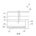
由於,側入式背光模組不具有區域調光之功能,使得對比度較差,而且在顯示面板的邊緣會有明顯的漏光,因此,許多的顯示面板採用直下式背光模組,尤其是使用倒裝發光二極體作為直下式背光模組的光源,請參閱圖2所示,直下式背光模組係在背光膜材20的下方設置反射片21,而倒裝發光二極體22設置在背光膜材20與反射片21之間,且倒裝發光二極體22由側面發出光源,再由反射片21將倒裝發光二極體22的光源反射朝向背光膜材20,藉以提高背光模組的亮度及色度的均勻性。Because the edge-type backlight module does not have the function of regional dimming, the contrast ratio is poor, and there will be obvious light leakage at the edge of the display panel. Therefore, many display panels use direct-type backlight modules, especially those using flip-chip The light emitting diode is used as the light source of the direct type backlight module. Please refer to FIG. 2. The direct type backlight module is provided with a
請參閱圖3所示,前述的倒裝發光二極體22由上至下依序包括第一反射層220、基板221、N型半導體層222、發光層223、P型半導體層224、第二反射層225,並且在N型半導體層222底面於相鄰發光層223、P型半導體層224、第二反射層225的側邊設有負電極226,第二反射層225的底面設有正電極227,在且負電極226周圍延伸到第二反射層225接近正電極227的位置設有絕緣層228,當負電極226及正電極227導通時,N型半導體層222及P型半導體層224產生的電子及電洞,將在發光層223結合而產生出相應波長的光源。Referring to FIG. 3 , the aforementioned flip-chip light-
但是傳統的第一反射層220與第二反射層225之間呈現平行,造成倒裝發光二極體22之光源在第一反射層220與第二反射層225之間反覆地繞射,進一步而言,光源在倒裝發光二極體的內部中繞射太久時間,導致出光效率太低,而且會產生高熱,故有必要針對此些問題進行改善。However, the conventional first
有鑑於先前技術的問題,本發明之目的係減少光源在倒裝發光二極體內部繞射時間,避免倒裝發光二極體產生高熱,並且達到讓光源快速地從側面出光之目的。In view of the problems of the prior art, the purpose of the present invention is to reduce the diffraction time of the light source inside the flip-chip light-emitting diode, avoid high heat generated by the flip-chip light-emitting diode, and achieve the purpose of allowing the light source to quickly emit light from the side.
根據本發明之目的,係提供一種倒裝發光二極體,包括基板、P-N二極管、第一反射層、導光層及第二反射層,P-N二極管設置在基板之一側,第一反射層設置在P-N二極管相對基板的一側,導光層設置在基板相對於P-N二極管層之一側,導光層背對基板的一面設有光路調整面,第二反射層設置在光路調整面上, P-N二極管所發出的光線在該第一反射層及該第二反射層之間反射,並朝向該倒裝發光二極體的側面出光。According to the purpose of the present invention, a flip-chip light-emitting diode is provided, which includes a substrate, a P-N diode, a first reflective layer, a light guide layer and a second reflective layer. The P-N diode is arranged on one side of the substrate, and the first reflective layer is arranged on one side. On the side of the P-N diode opposite to the substrate, the light guide layer is arranged on the side of the substrate opposite to the P-N diode layer, the side of the light guide layer facing away from the substrate is provided with an optical path adjustment surface, and the second reflection layer is arranged on the optical path adjustment surface, P-N The light emitted by the diode is reflected between the first reflection layer and the second reflection layer, and emits light toward the side of the flip-chip light emitting diode.
其中,P-N二極管自基板到第一反射層之間,係包括N型半導體層、P型半導體層及發光層,發光層在P型半導體層與N型半導體層的導電之狀態發出的光線,並在第一反射層及第二反射層之間反射,且朝向倒裝發光二極體的側面出光。The P-N diode from the substrate to the first reflective layer includes an N-type semiconductor layer, a P-type semiconductor layer and a light-emitting layer, and the light-emitting layer emits light in the conductive state of the P-type semiconductor layer and the N-type semiconductor layer, and It is reflected between the first reflective layer and the second reflective layer, and emits light toward the side of the flip-chip light emitting diode.
其中,倒裝發光二極體尚包括負電極、正電極及絕緣層,其中負電極設置在N型半導體層的底面相鄰發光層、P型半導體層、第一反射層的位置,正電極設在第一反射層的底部,絕緣層設在負電極的周圍,並沿著第一反射層的底部延伸到接近正電極的位置。The flip-chip light-emitting diode still includes a negative electrode, a positive electrode and an insulating layer, wherein the negative electrode is arranged on the bottom surface of the N-type semiconductor layer adjacent to the light-emitting layer, the P-type semiconductor layer, and the position of the first reflective layer, and the positive electrode is arranged At the bottom of the first reflective layer, an insulating layer is provided around the negative electrode and extends along the bottom of the first reflective layer to a position close to the positive electrode.
其中,基板係為藍寶石(sapphire)基板,組成為氧化鋁(Al2O3)。Among them, the substrate is a sapphire substrate, and the composition is aluminum oxide (Al2 O3 ).
其中,第一反射層係為分佈式布拉格反射器(Distributed Bragg Reflector)。The first reflection layer is a distributed Bragg reflector (Distributed Bragg Reflector).
其中,光路調整面為固定斜率的斜面,令導光層形成倒錐形體,或者光路調整面為漸變曲率的曲面,令導光層形成連續曲面體,且光路調整面的中央位置的切線之法線與光路調整面的任一位置的切線之法線具有夾角。Among them, the optical path adjustment surface is a slope with a fixed slope, so that the light guide layer forms an inverted cone, or the optical path adjustment surface is a curved surface with gradual curvature, so that the light guide layer forms a continuous curved surface, and the method of tangent to the central position of the optical path adjustment surface The line has an included angle with the normal of the tangent at any position of the light path adjustment surface.
其中,導光層於基板的投影面積大於基板,導光層中間位置的厚度為基板、P-N二極管及第一反射層的總和厚度的十分之一,進一步約為10~20微米(10~20μm),又導光層兩側邊緣的厚度與導光層中間位置的厚度之厚度差約為基板、P-N二極管及第一反射層的總和厚度的四分之一,進一步約為10~50微米(10~50μm)。The projected area of the light guide layer on the substrate is larger than that of the substrate, and the thickness of the middle position of the light guide layer is one-tenth of the total thickness of the substrate, the P-N diode and the first reflective layer, and is further about 10-20 μm (10-20 μm ), and the thickness difference between the thickness of the edge of the light guide layer and the thickness of the middle position of the light guide layer is about a quarter of the total thickness of the substrate, the P-N diode and the first reflective layer, and further about 10 to 50 microns ( 10~50μm).
根據本發明之目的,係一種背光模組,係包括複數個前述的倒裝發光二極體、電路板、背光膜材,各倒裝發光二極體係夾設在電路板與背光膜材之間,並在各倒裝發光二極體上設置保護層,且各倒裝發光二極體連接電路板。According to the purpose of the present invention, it is a backlight module, which includes a plurality of the aforementioned flip-chip light-emitting diodes, circuit boards, and backlight film materials, and each flip-chip light-emitting diode system is sandwiched between the circuit board and the backlight film material. , and a protective layer is arranged on each flip-chip light-emitting diode, and each flip-chip light-emitting diode is connected to the circuit board.
根據本發明之目的,係提供一種倒裝發光二極體之製造方法,包括下列步驟,提供一待製品,待製品包括一基板、複數個P-N二極管及複數個第一反射層,其中各P-N二極管設置在基板之一側,各第一反射層分別設置在其中一個P-N二極管相對於基板的一側,在基板相對於各P-N二極管之一側製作導光層,各導光層相對基板的一側為光路調整面,以及沿著光路調整面製作第二反射層,切割各導光層及其相對應的第二反射層直到基板面對各P-N二極管的一面為止,形成複數個倒裝發光二極體。According to the purpose of the present invention, a method for manufacturing flip-chip light-emitting diodes is provided, which includes the following steps, and provides a product to be prepared, the product to be prepared includes a substrate, a plurality of P-N diodes and a plurality of first reflective layers, wherein each P-N diode It is arranged on one side of the substrate, each first reflective layer is respectively arranged on one side of one of the P-N diodes opposite to the substrate, and a light guide layer is made on one side of the substrate opposite to each P-N diode, and each light guide layer is opposite to the side of the substrate. For the optical path adjustment surface and the second reflection layer along the optical path adjustment surface, each light guide layer and its corresponding second reflection layer are cut until the substrate faces the side of each P-N diode to form a plurality of flip-chip light emitting diodes body.
其中,製作導光層的步驟進一步包括:將光阻塗佈在基板相對於P-N二極管之一側,對光阻進行曝光,且對光阻的曝光強度分布係分別對應各P-N二極管的位置進行調整,對光阻進行顯影,完成顯影後光阻即形成導光層,並導光層在背對各P-N二極管分別形成光路調整面,且光路調整面與基板之間具有夾角。Wherein, the step of making the light guide layer further includes: coating a photoresist on one side of the substrate opposite to the P-N diode, exposing the photoresist, and adjusting the exposure intensity distribution of the photoresist corresponding to the position of each P-N diode respectively , develop the photoresist, and after the development is completed, the photoresist forms a light guide layer, and the light guide layer forms an optical path adjustment surface on the back of each P-N diode, and the optical path adjustment surface and the substrate have an included angle.
其中,在進行曝光的過程中,對光阻的曝光強度分布係針對各P-N二極管的中央往兩側漸變,對光阻進行顯影,完成顯影後光阻即形成導光層,且導光層在背對各P-N二極管形成光路調整面,各光路調整面的厚度以相對各P-N二極管中央到兩側逐漸增厚。Among them, in the process of exposure, the exposure intensity distribution of the photoresist is gradually changed from the center of each P-N diode to both sides, and the photoresist is developed. After the development is completed, the photoresist forms a light guide layer, and the light guide layer is in An optical path adjustment surface is formed facing away from each P-N diode, and the thickness of each optical path adjustment surface gradually increases relative to the center to both sides of each P-N diode.
其中,光阻為正型光刻膠,而當對光阻進行曝光時,係以半調色掩膜板設置在光源與光阻之間,利用半調色掩膜板調整光源的曝光強度從相對各P-N二極管的中央往兩側逐漸減弱。Among them, the photoresist is a positive type photoresist, and when the photoresist is exposed, a half-tone mask is set between the light source and the photoresist, and the half-tone mask is used to adjust the exposure intensity of the light source from Relative to the center of each P-N diode, it gradually weakens toward both sides.
其中,光阻為負型光刻膠,而當對光阻進行曝光時,係以半調色掩膜板設置在光源與光阻之間,利用半調色掩膜板調整光源的曝光強度從相對各P-N二極管的中央往兩側逐漸增強。Among them, the photoresist is a negative photoresist, and when the photoresist is exposed, a half-tone mask is set between the light source and the photoresist, and the half-tone mask is used to adjust the exposure intensity of the light source from Relative to the center of each P-N diode, it gradually increases toward both sides.
其中,切割為使用雷射切割機進行切割。Among them, the cutting is cutting using a laser cutting machine.
據上所述,與第一反射層與第二反射層將發光層所發出的光源朝向側面,減少光源在與第一反射層與第二反射層之間來回繞射,使得光源快速地朝向倒裝發光二極體的側面出光。此外,本發明係在倒裝發光二極體增設一個導光層,其餘的製程皆與傳統的倒裝發光二極體,故本發明在較低程度的流程就可以達到最佳的側面出光效果。According to the above, with the first reflective layer and the second reflective layer, the light source emitted by the light-emitting layer is directed to the side, reducing the back and forth diffraction of the light source between the first reflective layer and the second reflective layer, so that the light source rapidly faces the opposite direction. The side where the light-emitting diode is installed emits light. In addition, in the present invention, a light guide layer is added to the flip-chip light-emitting diode, and the rest of the manufacturing process is the same as that of the traditional flip-chip light-emitting diode, so the present invention can achieve the best side light emitting effect with a relatively low level of process. .
為了使本發明的目的、技術方案及優點更加清楚明白,下面結合附圖及實施例,對本發明進行進一步詳細說明。應當理解,此處所描述的具體實施例僅用以解釋本發明,但並不用於限定本發明。In order to make the objectives, technical solutions and advantages of the present invention clearer, the present invention will be further described in detail below with reference to the accompanying drawings and embodiments. It should be understood that the specific embodiments described herein are only used to explain the present invention, but not to limit the present invention.
請參閱圖4所示,本發明係一種倒裝發光二極體,係包括基板30、P-N二極管31、第一反射層32、導光層33及第二反射層34,P-N二極管31設置在基板30之一側,第一反射層32設置在P-N二極管31相對基板30的一側,導光層33設置在基板30相對於P-N二極管31層之一側,導光層33背對基板30的一面設有光路調整面330,第二反射層34設置在光路調整面330上,即形成倒裝發光二極體3, P-N二極管31所發出的光線在該第一反射層32及該第二反射層34之間反射,並朝向倒裝發光二極體3的側面出光。如此,即可解決傳統倒裝發光二極體來回反覆繞射但是不易從側面出光的問題,由於可以快速地出光也進一步解決傳統倒裝發光二極體產生高熱的問題。Please refer to FIG. 4 , the present invention is a flip-chip light emitting diode, which includes a
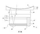
在本發明中,請參閱圖5所示,P-N二極管31自基板30到第一反射層32之間,係包括N型半導體層310、P型半導體層311及發光層312,其中N型半導體層310與P型半導體層311之間夾設發光層312,發光層312在N型半導體層310與P型半導體層311的導電之狀態發出的光線,並在第一反射層32及第二反射層34之間反射,且朝向第一反射層32及第二反射層34之間的側面出光。In the present invention, please refer to FIG. 5, the
在本發明中,請參閱圖5所示,倒裝發光二極體3尚包括負電極35、正電極36及絕緣層37,其中負電極35設置在N型半導體層310的底面相鄰發光層312、P型半導體層311、第一反射層32的位置,正電極36設在第一反射層32的底部,絕緣層37設在負電極35的周圍,並沿著第一反射層32的底部延伸到接近正電極36的位置。In the present invention, please refer to FIG. 5 , the flip-chip light-
據上所述,當導通負電極35及正電極36時,N型半導體層310及P型半導體層311產生的電子及電洞,電子及電洞將在發光層312結合,而在發光層312產生出相應波長的光源,此光源將在第一反射層32與第二反射層34之間反射,並朝向倒裝發光二極體3的側面出光。According to the above, when the
在本發明中,倒裝發光二極體3係為迷你發光二極體(Mini LED),其厚度約為200微米(200μm),基板30係為藍寶石(sapphire)基板30,組成為氧化鋁(Al2O3),N型半導體層310為N型氮化鎵(N-GaN)半導體層,P型半導體層311為P型氮化鎵(P-GaN)半導體層。第二反射層34係為分佈式布拉格反射器(Distributed Bragg Reflector),發光層312係為多量子井(Multiple Quantum Well,簡稱:MQW)。In the present invention, the flip-chip light-
在本發明中,請參閱圖6所示,光路調整面330為固定斜率的斜面,令導光層33形成倒錐形體,或者光路調整面330為漸變曲率的曲面,令導光層33形成連續曲面體(如圖5所示),且光路調整面330的中央位置的切線之法線與光路調整面330的任一位置的切線之法線具有夾角θ(如圖4所示),但本發明在實際實施時,並不限於此,舉凡光路調整面330之形狀可以使得光源快速被反射出光者,皆屬於本發明所稱之光路調整面330。第二反射層34可為銀薄膜、鋁薄膜、銀化合物薄膜或鋁化合物薄膜,但本發明於實際實施時,並不限於此,舉凡可以將光源反射到第一反射層3231之任一種具有反射能力之薄膜,皆屬於本發明所稱之第二反射層34。In the present invention, please refer to FIG. 6 , the optical
由於,若導光層33於基板30的投影面積與基板30相等,光源可能會由基板30與導光層33的位置漏光,甚至於導光層33於基板30的投影面積小於基板30,光源會朝向基板30的方向直接出光,因此,在本發明中,導光層33於基板30的投影面積大於基板30,將使得導光層33完全遮住基板30,而且導光層33突出基板的部分就如同帽子的帽沿,使得倒裝發光二極體3朝向基板30的方向出光的部分,可以被導光層33上所設置的第二反射層34反側,而可以減少或完全解決漏光或直接出光的問題。又,導光層33兩側邊緣的厚度(H1)與導光層33中間位置的厚度(H2)之厚度差約為基板30、P-N二極管31及第一反射層32的總和厚度的四分之一(意即約小於倒裝發光二極體3的四分之一),進一步約為10~50微米(10~20μm),導光層33中間位置的厚度(H2)為基板30、P-N二極管31及第一反射層32的總和厚度的十分之一(意即約為倒裝發光二極體3的十分之一),進一步約為10~20微米(10~20μm)。Because, if the projected area of the
請參閱圖7所示,本發明係一種背光模組,係包括複數個前述的倒裝發光二極體3、電路板4、背光膜材5,各倒裝發光二極體3係夾設在電路板4與背光膜材5之間,其中倒裝發光二極體3係為裸晶,為了避免損壞,各倒裝發光二極體3上設置保護層38,且各倒裝發光二極體3連接電路板4。如此,當電路板4可以傳送電力及輸出驅動訊號到各倒裝發光二極體3,使得各倒裝發光二極體3朝向背光膜材5發光,並且倒裝發光二極體3的光源可以有效地且均勻地朝向背光膜材5的方向發光。Referring to FIG. 7, the present invention is a backlight module, which includes a plurality of the aforementioned flip-chip light-
請參閱圖8所示,本發明係一種倒裝發光二極體之製造方法,包括下列步驟: (S101) 提供一待製品6,待製品包括一基板30、複數個P-N二極管31及複數個第一反射層32,其中各P-N二極管31設置在基板30之一側,各第一反射層32分別設置在其中一個P-N二極管31相對於基板30的一側; (S102) 在基板30相對於各P-N二極管31之一側製作導光層33,各導光層33相對基板30的一側為光路調整面330; (S103) 沿著光路調整面330製作第二反射層34;以及 (S104)切割各導光層33及其相對應的第二反射層34直到基板30面對各P-N二極管31的一面為止,形成複數個倒裝發光二極體。Please refer to FIG. 8 , the present invention is a manufacturing method of a flip-chip light-emitting diode, comprising the following steps: (S101) Provide a
綜上所述,本發明的倒裝發光二極體係在原本的傳統製程上增加製作導光層33,並未增加太多額外的製程及生產時間,但是可以大幅提高倒裝發光二極體從側面出光的效率。To sum up, the flip-chip light-emitting diode system of the present invention adds the fabrication of the
在本發明中,製作導光層33的步驟進一步包括: (S1021)將光阻7塗佈在基板30相對於P-N二極管31之一側; (S1022)對光阻7進行曝光,且對光阻7的曝光強度分布係分別對應各P-N二極管31的位置進行調整; (S1023)對光阻7進行顯影,完成顯影後光阻7即形成導光層33,並導光層33在背對各P-N二極管31分別形成光路調整面330,且光路調整面330與基板30之間具有夾角。In the present invention, the step of making the
在本發明中,在進行曝光的過程中,對光阻7的曝光強度分布係針對各P-N二極管31的中央往兩側漸變,對光阻7進行顯影,完成顯影後光阻7即形成導光層33,且導光層33在背對各P-N二極管31形成光路調整面330,各光路調整面330的厚度以相對各P-N二極管31中央到兩側逐漸增厚。In the present invention, during the exposure process, the exposure intensity distribution of the
在本發明中,光阻7為正型光刻膠,而當對光阻7進行曝光時,係以半調色掩膜板8設置在光源與光阻7之間,利用半調色掩膜板8調整光源的曝光強度從相對各P-N二極管31的中央往兩側逐漸減弱。光阻7為負型光刻膠,而當對光阻7進行曝光時,係以半調色掩膜板8設置在光源與光阻7之間,利用半調色掩膜板8調整光源的曝光強度從相對各P-N二極管31的中央往兩側逐漸增強。其中切割為使用雷射切割機9進行切割。In the present invention, the
綜上所述,發光層312所發出的光源從第一反射層31與第二反射層34之間反射直到從倒裝發光二極體3的側面出光,減少光源在倒裝發光二極體3內部來回繞射,進而可以增加發光效率,同時減少產生熱能。再者,本發明僅增設一個導光層33的製作流程,其餘的製程皆與傳統的倒裝發光二極體3雷同,故本發明在較低程度的流程就可以達到最佳的側面出光效果。To sum up, the light source emitted by the light-emitting
上列詳細說明係針對本發明的可行實施例之具體說明,惟前述的實施例並非用以限制本發明之專利範圍,凡未脫離本發明技藝精神所為之等效實施或變更,均應包含於本案之專利範圍中。The above detailed descriptions are specific descriptions of feasible embodiments of the present invention, but the foregoing embodiments are not intended to limit the patent scope of the present invention. Any equivalent implementation or modification that does not depart from the technical spirit of the present invention shall be included in the within the scope of the patent in this case.
10:正裝發光二極體 11、20、5:背光膜材 12:導光板 13、21:反射片 22、3:倒裝發光二極體 220、34:第二反射層 221、30:基板 31:P-N二極管 222、310:N型半導體層 223、312:發光層 224、311:P型半導體層 225、32:第一反射層 33:導光層 330:光路調整面 226、35:負電極 227、36:正電極 228、37:絕緣層 38:保護層 4:電路板 5:背光膜材 6:待製品 7:光阻 8:半調色掩膜板 9:雷射切割器 θ:夾角 H1:導光層兩側邊緣的厚度 H2:導光層中間位置的厚度 S101~S104:步驟 S1021~S1023:步驟10: formal installation of light-emitting
圖1係傳統側入式背光模組之示意圖。 圖2係傳統直下式背光模組之示意圖。 圖3係傳統倒裝發光二極體之示意圖。 圖4係本發明之倒裝發光二極體之示意圖。 圖5係本發明之第一實施例的倒裝發光二極體之示意圖。 圖6係本發明之第二實施例的倒裝發光二極體之示意圖。 圖7係本發明之背光模組之示意圖。 圖8係本發明之側光式倒裝發光二極體之製作流程示意圖。FIG. 1 is a schematic diagram of a conventional edge-lit backlight module. FIG. 2 is a schematic diagram of a conventional direct type backlight module. FIG. 3 is a schematic diagram of a conventional flip-chip light emitting diode. FIG. 4 is a schematic diagram of the flip-chip light emitting diode of the present invention. FIG. 5 is a schematic diagram of a flip-chip light emitting diode according to the first embodiment of the present invention. FIG. 6 is a schematic diagram of a flip-chip light emitting diode according to a second embodiment of the present invention. FIG. 7 is a schematic diagram of the backlight module of the present invention. FIG. 8 is a schematic diagram of the manufacturing process of the edge-lit flip-chip light emitting diode of the present invention.
3:倒裝發光二極體3: Flip chip light-emitting diode
30:基板30: Substrate
31:P-N二極管31: P-N diode
32:第一反射層32: The first reflective layer
33:導光層33: light guide layer
330:光路調整面330: Optical path adjustment surface
34:第二反射層34: Second reflective layer
θ:夾角θ: included angle
H1:導光層兩側邊緣的厚度H1: The thickness of the edges on both sides of the light guide layer
H2:導光層中間位置的厚度H2: Thickness at the middle of the light guide layer
Claims (4)
Translated fromChineseApplications Claiming Priority (2)
| Application Number | Priority Date | Filing Date | Title |
|---|---|---|---|
| CN202110160209.4 | 2021-02-05 | ||
| CN202110160209.4ACN112992877B (en) | 2021-02-05 | 2021-02-05 | Flip-chip light emitting diode, manufacturing method thereof and backlight module |
Publications (2)
| Publication Number | Publication Date |
|---|---|
| TWI765568Btrue TWI765568B (en) | 2022-05-21 |
| TW202232789A TW202232789A (en) | 2022-08-16 |
Family
ID=76347965
Family Applications (1)
| Application Number | Title | Priority Date | Filing Date |
|---|---|---|---|
| TW110104719ATWI765568B (en) | 2021-02-05 | 2021-02-08 | Flip-chip light-emitting diode, manufacturing method and backlight module therefor |
Country Status (2)
| Country | Link |
|---|---|
| CN (1) | CN112992877B (en) |
| TW (1) | TWI765568B (en) |
Families Citing this family (2)
| Publication number | Priority date | Publication date | Assignee | Title |
|---|---|---|---|---|
| CN113359352B (en)* | 2021-07-01 | 2022-09-20 | 业成科技(成都)有限公司 | Direct type backlight module and display thereof |
| CN113903845B (en)* | 2021-08-25 | 2023-12-22 | 华灿光电(浙江)有限公司 | Micro light-emitting diode chip and preparation method thereof |
Citations (2)
| Publication number | Priority date | Publication date | Assignee | Title |
|---|---|---|---|---|
| TW200924238A (en)* | 2007-07-30 | 2009-06-01 | Philips Lumileds Lighting Co | Concave wide emitting lens for LED useful for backlighting |
| CN111312068A (en)* | 2020-04-02 | 2020-06-19 | 深圳创维-Rgb电子有限公司 | Mini lamp bead, manufacturing method, backlight source and display device |
Family Cites Families (10)
| Publication number | Priority date | Publication date | Assignee | Title |
|---|---|---|---|---|
| US7626210B2 (en)* | 2006-06-09 | 2009-12-01 | Philips Lumileds Lighting Company, Llc | Low profile side emitting LED |
| CN101859861A (en)* | 2010-05-13 | 2010-10-13 | 厦门市三安光电科技有限公司 | GaN-based flip-chip light-emitting diode with double reflecting layers and preparation method thereof |
| CN101872824A (en)* | 2010-06-07 | 2010-10-27 | 厦门市三安光电科技有限公司 | Gallium nitride-based flip-chip light-emitting diode with double reflective layers on side and preparation method thereof |
| CN102130248A (en)* | 2010-10-08 | 2011-07-20 | 映瑞光电科技(上海)有限公司 | Light emitting device and manufacturing method thereof |
| KR102001665B1 (en)* | 2012-08-31 | 2019-07-18 | 서울반도체 주식회사 | Light emitting module for surface illumination |
| TWI610470B (en)* | 2016-06-13 | 2018-01-01 | 隆達電子股份有限公司 | Light-emitting diode wafer level package structure, direct-type backlight module and manufacturing method of light-emitting device |
| JP7021485B2 (en)* | 2017-09-21 | 2022-02-17 | 富士フイルムビジネスイノベーション株式会社 | Luminous components, printheads and image forming equipment |
| KR20190058770A (en)* | 2017-11-22 | 2019-05-30 | 주식회사 루멘스 | Light emitting diode module and manufacturing method thereof |
| CN110034220B (en)* | 2019-04-16 | 2024-06-25 | 佛山市国星半导体技术有限公司 | A flip-chip LED chip and its manufacturing method |
| CN112289915B (en)* | 2020-09-14 | 2021-11-05 | 华灿光电(浙江)有限公司 | Flip light-emitting diode chip and manufacturing method thereof |
- 2021
- 2021-02-05CNCN202110160209.4Apatent/CN112992877B/enactiveActive
- 2021-02-08TWTW110104719Apatent/TWI765568B/enactive
Patent Citations (2)
| Publication number | Priority date | Publication date | Assignee | Title |
|---|---|---|---|---|
| TW200924238A (en)* | 2007-07-30 | 2009-06-01 | Philips Lumileds Lighting Co | Concave wide emitting lens for LED useful for backlighting |
| CN111312068A (en)* | 2020-04-02 | 2020-06-19 | 深圳创维-Rgb电子有限公司 | Mini lamp bead, manufacturing method, backlight source and display device |
Also Published As
| Publication number | Publication date |
|---|---|
| CN112992877A (en) | 2021-06-18 |
| TW202232789A (en) | 2022-08-16 |
| CN112992877B (en) | 2022-11-22 |
Similar Documents
| Publication | Publication Date | Title |
|---|---|---|
| TWI665810B (en) | Light emitting diode chip having distributed bragg reflector | |
| US11935990B2 (en) | Light emitting diode having side reflection layer | |
| JP6600521B2 (en) | Lens and light emitting element module including the same | |
| JP7026612B2 (en) | Backlight, backlight manufacturing method, light guide plate, light guide plate manufacturing method and display device | |
| US10937925B2 (en) | Light emitting diode chip having distributed Bragg reflector | |
| KR102801220B1 (en) | Light source module and display panel using the same | |
| US20090032827A1 (en) | Concave Wide Emitting Lens for LED Useful for Backlighting | |
| KR101791175B1 (en) | Light emitting device and light emitting device package including the same | |
| TWI765568B (en) | Flip-chip light-emitting diode, manufacturing method and backlight module therefor | |
| CN112687775A (en) | Light-emitting diode | |
| US20220085258A1 (en) | Spacer layer arrangements for light-emitting diodes | |
| KR20160057146A (en) | A light emitting device package | |
| US20240313179A1 (en) | Unit pixel having light emitting device and displaying apparatus | |
| US20250022856A1 (en) | Unit pixel and displaying apparatus including the unit pixel | |
| CN111164770B (en) | Micro light-emitting diode chip, manufacturing method thereof and display device | |
| TWM609027U (en) | Light source module and display device | |
| US12080687B2 (en) | Unit pixel having light emitting device, method of fabricating the same, and displaying apparatus having the same | |
| TW202036935A (en) | Light source module and display apparatus | |
| US20240113150A1 (en) | Light emitting device and light emitting module having the same | |
| KR20250133364A (en) | Sidewall arrays and related methods for light-emitting diode devices | |
| CN114551669B (en) | A light emitting device and a method for manufacturing the same, and a display device | |
| KR101983779B1 (en) | A light emitting device package | |
| KR101850435B1 (en) | A light emitting module, and a display apparatus | |
| US12439758B2 (en) | Wafer having auxiliary pattern for aligning light emitting device and method of fabricating unit pixel using the same | |
| KR102050058B1 (en) | A light emitting device package |