TWI765132B - Antenna structure - Google Patents
Antenna structureDownload PDFInfo
- Publication number
- TWI765132B TWI765132BTW107147018ATW107147018ATWI765132BTW I765132 BTWI765132 BTW I765132BTW 107147018 ATW107147018 ATW 107147018ATW 107147018 ATW107147018 ATW 107147018ATW I765132 BTWI765132 BTW I765132B
- Authority
- TW
- Taiwan
- Prior art keywords
- switch
- vertical
- radiator
- antenna structure
- planar metal
- Prior art date
Links
- 229910052751metalInorganic materials0.000claimsabstractdescription156
- 239000002184metalSubstances0.000claimsabstractdescription156
- 239000000758substrateSubstances0.000claimsabstractdescription73
- 239000004020conductorSubstances0.000claimsabstractdescription47
- 230000005855radiationEffects0.000claimsdescription19
- 230000000149penetrating effectEffects0.000claims1
- PXHVJJICTQNCMI-UHFFFAOYSA-NNickelChemical compound[Ni]PXHVJJICTQNCMI-UHFFFAOYSA-N0.000description6
- 230000005540biological transmissionEffects0.000description6
- 238000004806packaging method and processMethods0.000description5
- 238000013461designMethods0.000description4
- 238000010586diagramMethods0.000description4
- 238000000034methodMethods0.000description4
- 230000010287polarizationEffects0.000description4
- RYGMFSIKBFXOCR-UHFFFAOYSA-NCopperChemical compound[Cu]RYGMFSIKBFXOCR-UHFFFAOYSA-N0.000description3
- 229910052782aluminiumInorganic materials0.000description3
- XAGFODPZIPBFFR-UHFFFAOYSA-NaluminiumChemical compound[Al]XAGFODPZIPBFFR-UHFFFAOYSA-N0.000description3
- 229910052802copperInorganic materials0.000description3
- 239000010949copperSubstances0.000description3
- PCHJSUWPFVWCPO-UHFFFAOYSA-NgoldChemical compound[Au]PCHJSUWPFVWCPO-UHFFFAOYSA-N0.000description3
- 229910052737goldInorganic materials0.000description3
- 239000010931goldSubstances0.000description3
- 150000002739metalsChemical class0.000description3
- 238000012986modificationMethods0.000description3
- 230000004048modificationEffects0.000description3
- 229910052759nickelInorganic materials0.000description3
- 239000004593EpoxySubstances0.000description2
- 230000001154acute effectEffects0.000description2
- 239000000919ceramicSubstances0.000description2
- 238000004891communicationMethods0.000description2
- 230000005669field effectEffects0.000description2
- 239000011810insulating materialSubstances0.000description2
- 239000000463materialSubstances0.000description2
- ATJFFYVFTNAWJD-UHFFFAOYSA-NTinChemical compound[Sn]ATJFFYVFTNAWJD-UHFFFAOYSA-N0.000description1
- 229910045601alloyInorganic materials0.000description1
- 239000000956alloySubstances0.000description1
- 230000009286beneficial effectEffects0.000description1
- 230000001364causal effectEffects0.000description1
- 239000011248coating agentSubstances0.000description1
- 238000000576coating methodMethods0.000description1
- 238000011161developmentMethods0.000description1
- 238000005516engineering processMethods0.000description1
- 239000011521glassSubstances0.000description1
- 230000002452interceptive effectEffects0.000description1
- 239000007788liquidSubstances0.000description1
- 229910044991metal oxideInorganic materials0.000description1
- 150000004706metal oxidesChemical class0.000description1
- 238000010295mobile communicationMethods0.000description1
- 239000003973paintSubstances0.000description1
- 238000007747platingMethods0.000description1
- 239000004065semiconductorSubstances0.000description1
- 230000008054signal transmissionEffects0.000description1
- 239000010703siliconSubstances0.000description1
- 229910052710siliconInorganic materials0.000description1
- 229910000679solderInorganic materials0.000description1
Images


Classifications
- H—ELECTRICITY
- H01—ELECTRIC ELEMENTS
- H01Q—ANTENNAS, i.e. RADIO AERIALS
- H01Q1/00—Details of, or arrangements associated with, antennas
- H01Q1/12—Supports; Mounting means
- H01Q1/22—Supports; Mounting means by structural association with other equipment or articles
- H01Q1/2283—Supports; Mounting means by structural association with other equipment or articles mounted in or on the surface of a semiconductor substrate as a chip-type antenna or integrated with other components into an IC package
- H—ELECTRICITY
- H01—ELECTRIC ELEMENTS
- H01Q—ANTENNAS, i.e. RADIO AERIALS
- H01Q3/00—Arrangements for changing or varying the orientation or the shape of the directional pattern of the waves radiated from an antenna or antenna system
- H01Q3/24—Arrangements for changing or varying the orientation or the shape of the directional pattern of the waves radiated from an antenna or antenna system varying the orientation by switching energy from one active radiating element to another, e.g. for beam switching
- H—ELECTRICITY
- H01—ELECTRIC ELEMENTS
- H01Q—ANTENNAS, i.e. RADIO AERIALS
- H01Q1/00—Details of, or arrangements associated with, antennas
- H01Q1/36—Structural form of radiating elements, e.g. cone, spiral, umbrella; Particular materials used therewith
- H—ELECTRICITY
- H01—ELECTRIC ELEMENTS
- H01Q—ANTENNAS, i.e. RADIO AERIALS
- H01Q1/00—Details of, or arrangements associated with, antennas
- H01Q1/50—Structural association of antennas with earthing switches, lead-in devices or lightning protectors
- H—ELECTRICITY
- H01—ELECTRIC ELEMENTS
- H01Q—ANTENNAS, i.e. RADIO AERIALS
- H01Q21/00—Antenna arrays or systems
- H01Q21/06—Arrays of individually energised antenna units similarly polarised and spaced apart
- H01Q21/061—Two dimensional planar arrays
- H01Q21/064—Two dimensional planar arrays using horn or slot aerials
- H—ELECTRICITY
- H01—ELECTRIC ELEMENTS
- H01Q—ANTENNAS, i.e. RADIO AERIALS
- H01Q21/00—Antenna arrays or systems
- H01Q21/24—Combinations of antenna units polarised in different directions for transmitting or receiving circularly and elliptically polarised waves or waves linearly polarised in any direction
- H01Q21/245—Combinations of antenna units polarised in different directions for transmitting or receiving circularly and elliptically polarised waves or waves linearly polarised in any direction provided with means for varying the polarisation
- H—ELECTRICITY
- H01—ELECTRIC ELEMENTS
- H01Q—ANTENNAS, i.e. RADIO AERIALS
- H01Q9/00—Electrically-short antennas having dimensions not more than twice the operating wavelength and consisting of conductive active radiating elements
- H01Q9/04—Resonant antennas
- H01Q9/0407—Substantially flat resonant element parallel to ground plane, e.g. patch antenna
Landscapes
- Engineering & Computer Science (AREA)
- Microelectronics & Electronic Packaging (AREA)
- Variable-Direction Aerials And Aerial Arrays (AREA)
- Support Of Aerials (AREA)
- Details Of Aerials (AREA)
Abstract
Description
Translated fromChinese本發明是指一種天線結構,且特別是指一種可切換輻射場型的天線結構。The present invention refers to an antenna structure, and particularly to an antenna structure with a switchable radiation pattern.
隨著通訊技術的蓬勃發展,商用行動通訊系統已可達成在高速數據傳輸,且利於網路服務業者提供各式各樣的服務,例如多媒體影音串流、即時路況報導和行車導航以及即時網路通訊等需要龐大資料傳輸量的網路服務。對於硬體方面而言,天線的設計影響無線訊號的傳輸和接收效能。此外,習知天線不具有輻射場型切換功能,故其效能容易受到所在環境的限制。因此,如何設計出高效能的天線,為相關產業所致力的其中一個目標。With the vigorous development of communication technology, commercial mobile communication systems have achieved high-speed data transmission, which is beneficial for Internet service providers to provide various services, such as multimedia video streaming, real-time traffic reports and driving navigation, and real-time Internet Communication and other network services that require a large amount of data transmission. In terms of hardware, the design of the antenna affects the transmission and reception performance of wireless signals. In addition, the conventional antenna does not have a radiation field switching function, so its performance is easily limited by the environment in which it is located. Therefore, how to design a high-efficiency antenna is one of the goals that related industries are working on.
本發明的目的是在於提供一種天線結構,其具有輻射場型切換功能,可依據所在環境切換其產生的輻射場型,故在不同環境下均可具有高傳輸和接收效能。The purpose of the present invention is to provide an antenna structure with a radiation pattern switching function, which can switch the generated radiation pattern according to the environment, so that it can have high transmission and reception efficiency in different environments.
本發明之一方面是有關於一種天線結構,其包含基板、水平輻射體和垂直輻射體。水平輻射體位於基板上或基板中。垂直輻射體位於基板中且包含垂直導體、多個平面金屬結構和開關。此些平面金屬結構經由垂直導體彼此電性連接。開關位於此些平面金屬結構之缺口中且耦接此些平面金屬結構中之至少一者,其用以切換垂直輻射體之電流分佈。One aspect of the present invention pertains to an antenna structure comprising a substrate, a horizontal radiator, and a vertical radiator. The horizontal radiator is located on the base plateor in the substrate. A vertical radiator is located in the substrate and includes vertical conductors, a plurality of planar metal structures, and switches. The planar metal structures are electrically connected to each other through vertical conductors. A switch is located in the notches of the planar metal structures and coupled to at least one of the planar metal structures, and is used to switch the current distribution of the vertical radiator.
本發明之另一方面是有關於一種天線結構,其包含基板、水平輻射體、垂直輻射體和金屬分支。水平輻射體位於基板上或基板中。垂直輻射體位於基板中且包含垂直導體和多個平面金屬結構。此些平面金屬結構經由垂直導體彼此電性連接。金屬分支選擇性地耦接至垂直輻射體。Another aspect of the present invention relates to an antenna structure comprising a substrate, a horizontal radiator, a vertical radiator and a metal branch. The horizontal radiator is located on or in the substrate. The vertical radiator is located in the substrate and includes vertical conductors and a plurality of planar metal structures. The planar metal structures are electrically connected to each other through vertical conductors. The metal branch is selectively coupled to the vertical radiator.
本發明之另一方面是有關於一種天線結構,其包含基板、水平輻射體、垂直輻射體和金屬分支。水平輻射體位於基板上或基板中。垂直輻射體位於基板中且包含垂直導體、多個平面金屬結構和開關。此些平面金屬結構經由垂直導體彼此電性連接。開關位於此些平面金屬結構之缺口中且耦接此些平面金屬結構中之至少一者,其用以切換垂直輻射體之電流分佈。金屬分支選擇性地耦接至垂直輻射體。Another aspect of the present invention relates to an antenna structure comprising a substrate, a horizontal radiator, a vertical radiator and a metal branch. The horizontal radiator is located on or in the substrate. A vertical radiator is located in the substrate and includes vertical conductors, a plurality of planar metal structures, and switches. The planar metal structures are electrically connected to each other through vertical conductors. A switch is located in the notches of the planar metal structures and coupled to at least one of the planar metal structures, and is used to switch the current distribution of the vertical radiator. The metal branch is selectively coupled to the vertical radiator.
100、300、300'、300":天線結構100, 300, 300' , 300" : Antenna structure
110、310:基板110, 310: substrate
110A、310A:中央區110A, 310A: Central District
110B、310B:邊緣區110B, 310B: Marginal area
112:介電層112: Dielectric layer
114:金屬層114: Metal layer
310E:側邊310E: Side
312:導線312: Wire
314:導孔結構314: Guide hole structure
316:接合墊316: Bond pads
320:垂直輻射體320: Vertical Radiator
320A:垂直導體320A: Vertical conductor
320B:平面金屬結構320B: Planar Metal Structures
320B':分支320B' : Branch
320C:開關320C: switch
322、332:饋入線322, 332: feed line
324:金屬分支324: Metal Branch
330:水平輻射體330: Horizontal Radiator
340:晶片340: Wafer
342:金屬凸塊342: Metal bumps
θ、Φ:夾角θ, Φ: included angle
為了更完整了解實施例及其優點,現參照結合所附圖式所做之下列描述,其中:〔圖1A〕和〔圖1B〕分別為天線結構的立體圖和上視圖;〔圖2〕為〔圖1A〕之天線結構的側視圖;〔圖3〕為依據本發明一些實施例之天線結構的局部結構示意圖;〔圖4〕為〔圖3〕之天線結構的局部平面圖之一示例;〔圖5〕為〔圖3〕之天線結構的局部立體圖之一示例;〔圖6〕為依據本發明另一些實施例之天線結構的局部結構示意圖;〔圖7〕為〔圖6〕之天線結構的局部平面圖之一示例;〔圖8〕為依據本發明又一些實施例之天線結構的局部結構示意圖;以及〔圖9〕為〔圖8〕之天線結構的局部立體圖之一示例。For a more complete understanding of the embodiments and their advantages, reference is now made to the following description in conjunction with the accompanying drawings, wherein: [FIG. 1A] and [FIG. 1B] are a perspective view and a top view of an antenna structure, respectively; [FIG. 2] is [ 1A] is a side view of the antenna structure; [FIG. 3] is a partial structural representation of the antenna structure according to some embodiments of the present invention[Fig. 4] is an example of a partial plan view of the antenna structure of [Fig. 3]; [Fig. 5] is an example of a partial perspective view of the antenna structure of [Fig. 3]; [Fig. 6] is another example according to the present invention [FIG. 7] is an example of a partial plan view of the antenna structure of [FIG. 6]; [FIG. 8] is a schematic diagram of the partial structure of the antenna structure according to some embodiments of the present invention; and [FIG. 9] is an example of a partial perspective view of the antenna structure of [FIG. 8].
以下將以圖式及詳細敘述清楚說明本揭示內容之精神,任何所屬技術領域中具有通常知識者在瞭解本揭示內容之較佳實施例後,當可由本揭示內容所教示之技術,加以改變及修飾,其並不脫離本揭示內容之精神與範圍。The following will clearly illustrate the spirit of the present disclosure with drawings and detailed descriptions. Anyone with ordinary knowledge in the technical field, after understanding the preferred embodiments of the present disclosure, may be able to make changes and modifications by the techniques taught in the present disclosure. modifications, which do not depart from the spirit and scope of this disclosure.
在本文中所使用的用語僅是為了描述特定實施例,非用以限制申請專利範圍。除非另有限制,否則單數形式的「一」或「該」用語也可用來表示複數形式。此外,空間相對性用語的使用是為了說明元件在使用或操作時的不同方位,而不只限於圖式所繪示的方向。元件也可以其他方式定向(旋轉90度或在其他方向),而在此使用的空間相對性描述也可以相同方式解讀。The terms used herein are for the purpose of describing particular embodiments only and are not intended to limit the scope of the claims. Unless otherwise limited, the singular form "a" or "the" may also be used to refer to the plural form. In addition, the use of spatially relative terms is intended to describe different orientations of elements in use or operation, and is not limited to the orientation shown in the drawings. Elements may also be otherwise oriented (rotated 90 degrees or at other orientations) and the spatially relative descriptions used herein may be interpreted in the same manner.
為了簡化和明確說明,本文可能會在各種實施例中重複使用元件符號和/或字母,但這並不表示所討論的各種實施例及/或配置之間有因果關係。For simplicity and clarity of illustration, reference numerals and/or letters may be repeated in various embodiments herein, but this does not imply that the discussedThere is a causal relationship between the various embodiments and/or configurations.
另外,在本文中可能會使用空間相對用語,例如「上方(over)」、「上(on)」、「下方(under)」、「下(below)」等等,以方便說明如圖式所繪示之一元件或一特徵與另一元件或特徵之關係。除了在圖式中所繪示之方向外,這些空間相對用詞意欲含括元件在使用或操作中的不同方位。In addition, spatially relative terms, such as "over", "on", "under", "below", etc., may be used in this document to facilitate the description as shown in the drawings. Shows the relationship of one element or feature to another element or feature. These spatially relative terms are intended to encompass different orientations of the elements in use or operation other than the orientation depicted in the figures.
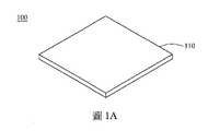
請參照圖1A和圖1B,圖1A和圖1B分別為天線結構100的立體圖和上視圖。天線結構100至少包含基板110和設置在基板110上或基板110中的元件,例如輻射元件、導線、開關和/或其他元件。基板110具有中央區110A和邊緣區110B,其中在中央區110A中具有傳輸電子訊號的元件,而在邊緣區中110B具有輻射體。Please refer to FIG. 1A and FIG. 1B , which are a perspective view and a top view of the
圖2為圖1A之天線結構100的側視圖。如圖2所示,基板110為多層板結構,其可由多個介電層112和多個金屬層114交互堆疊而成。每一介電層112可由FR4材料、玻璃、陶瓷、環氧樹脂或矽形成,而每一金屬層114可由銅、鋁、鎳和/或其他金屬形成。此外,每一金屬層114可包含輻射元件、導線、開關或其他形成輻射結構和電子訊號傳輸結構所需的元件。依據在金屬層114中形成的元件,金屬層114可具有不同的圖案。此外,依據介電層112的材料種類,基板110可藉由不同由低溫陶瓷共燒(low-temperature cofired ceramic;LTCC)、整合被動元件(integrated passive device;IPD)、多層薄膜、多層印刷電路板或其他多層製程來形成。FIG. 2 is a side view of the
圖3為依據本發明一些實施例之天線結構300的局部結構示意圖。如圖3所示,在基板310的中央區310A中配置有導線312、導孔結構314和/或其他元件,而在基板310的邊緣區310B中配置有垂直輻射體320和水平輻射體330,其可共同形成單極化或雙極化天線。基板310可以是多層板結構,其相似於如圖2所示以介電層112和金屬層114交互堆疊而成的結構。FIG. 3 is a schematic diagram of a partial structure of an
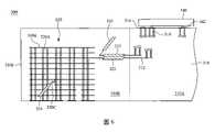
垂直輻射體320可上下橫跨基板310中的多層介電層。垂直輻射體320包含垂直導體320A、平面金屬結構320B和開關320C。垂直導體320A是沿著垂直基板310平面的方向延伸,而平面金屬結構320B是沿著基板310的平面方向延伸,其透過垂直導體320A彼此電性連接。在本實施例中,相鄰垂直導體320A之間的距離小於電磁波在基板310中的四分之一個等效波長。如圖3所示,在一些實施例中,垂直導體320A的長度相同,且在基板310中的高度位置亦相同。而在其他實施例中,垂直導體320A可具有不同的長度和/或不同的高度位置。The
在一些實施例中,垂直導體320A是由基板貫孔(through substrate via;TSV)導體所形成。在實作上,基板貫孔導體可藉由製程上塗佈導電液/漆或鍍上導電金屬,而令其具有導電之效果。In some embodiments, the
導孔結構314和垂直導體320A可由一或多種類型所組成。如圖3所示,導孔結構314包含盲孔(blind via)結構和埋孔(buried via)結構,而垂直導體320A為盲孔結構。然而,本發明實施例並不以此為限。在各實施例中,導孔結構314和/或垂直導體320A可包含盲孔結構、埋孔結構和/或通孔結構(through via),其可依據設計需求而決定。Via
此外,導孔結構314和垂直導體320A可以是電鍍(plated)導孔結構,其在導孔的孔壁上鍍有導電材料,例如銅、金、鋁、鎳或其他金屬等,而在剩餘的間隙中可填充或塞入導電材料或絕緣材料(例如空氣或環氧樹脂),或者是塞入導電材料或絕緣材料而形成塞孔(plugged via)結構,或者是在間隙的頂部和/或底部佈上防焊層(solder mask)而形成掩孔(tented via)結構。在其他實施例中,導孔結構314和垂直導體320A可以是非電鍍(non-plated)導孔結構,其在導孔中直接填充導電材料,例如銅、金、鋁、鎳等金屬,但不限於此。In addition, the via
平面金屬結構320B可分別屬於基板310中的若干金屬層。平面金屬結構320B的長度方向為垂直輻射體320的主波束水平方向。如圖3所示,在一些實施例中,平面金屬結構320B的長度相同且均大於電磁波在基板310中的四分之一個等效波長。而在其他實施例中,平面金屬結構320B可具有不同的長度,且平面金屬結構320B的最大長度大於電磁波在基板310中的四分之一個等效波長。此外,在一些實施例中,如圖3所示,平面金屬結構320B為金屬條。而在其他實施例中,平面金屬結構320B具有一或多個開槽孔之金屬片、上述金屬條和金屬片之組合,或是其他合適的金屬結構。The
平面金屬結構320B可具有一或多個平面圖案。以圖3之實施例而言,第一平面金屬結構320B(即由最底下算起的第一個平面金屬結構320B)具有兩個缺口,而每一第二至第四平面金屬結構320B具有一個缺口,其中在第二至第四平面金屬結構320B的缺口中分別具有開關320C。依據垂直導體320A在基板310中的配置,部份或全部缺口的寬度可小於兩相鄰垂直導體320A的距離,或者部份或全部缺口的寬度可大於兩相鄰垂直導體320A的距離。藉由控制開關320C的狀態,可決定在開關320C兩端的金屬結構是否可直接經由開關320C電性連接。當開關320C導通時,在開關320C兩側的金屬結構直接經由開關320C電性連接,即有電流流經開關320C,而當開關320C關斷時,在開關320C兩側的金屬結構不直接經由開關320C電性連接,即阻斷垂直輻射體320中的電流流經開關320C。由於電流分佈決定垂直輻射體320產生的輻射場型,故經由控制每一開關320C導通和關斷狀態,可決定垂直輻射體320的天線增益和產生的輻射場型圖案,包含主波束方向、半功率波束寬(half-power beam width;HPBW)和指向性等。以圖3之實施例而言,垂直輻射體320在每一開關320C導通時所產生之輻射場型的主波束方向較每一開關320C關斷時所產生之輻射場型的主波束方向偏上。因此,藉由導通或關斷每一開關320C,可切換天線結構300的輻射場型。The
依據基板310的種類和製程,每一開關320C可以是二極體、平面場效電晶體(field effect transistor;FET)、金氧半(metal oxide semiconductor;MOS)場效電晶體或上述組合,但不限於此。Depending on the type and process of the
水平輻射體330為平面金屬片結構,其長度可大約為電磁波在基板310中的四分之一個等效波長。水平輻射體330可以與平面金屬結構320B中之一者共平面,即屬於基板310中的同一金屬層,其決定垂直輻射體320的主波束垂直方向。The
如圖3所示,垂直輻射體320較水平輻射體330接近基板310的側邊310E。而在其他實施例中,水平輻射體330可較垂直輻射體320接近基板310的側邊310E,或者水平輻射體330與基板310的側邊310E之間的距離近似於垂直輻射體320與基板310的側邊310E之間的距離。As shown in FIG. 3 , the
垂直輻射體320和水平輻射體330分別經由饋入線322、332電性耦接至位於基板310中且在中央區310A的導線312、導孔結構314和/或其他元件。饋入線322可與平面金屬結構320B中之一者屬於基板310中的同一金屬層,且饋入線332可與水平輻射體330屬於基板310中的同一金屬層。饋入線322、332可以是平行微帶線結構或是其他傳輸線結構。The
此外,在基板310的中央區310A上方另設置晶片340,且晶片340之朝向基板310的側面上具有多個金屬凸塊342。透過將金屬凸塊342接合至在基板310上的接合墊316,可使晶片340安裝在基板310上,且可使在晶片340中的元件與在基板310中的導線312、導孔結構314和/或其他元件彼此電性連接,進而使得晶片340與垂直輻射體320和水平輻射體330電性連接。金屬凸塊342可以是金凸塊、錫凸塊或由其他金屬或合金形成的凸塊。In addition, a
晶片340具有射頻積體電路和/或其他構成傳輸和/或接收電路的主動和/或被動元件。晶片340可透過例如球柵陣列(ball grid array;BGA)封裝、晶粒尺寸封裝(chip scale packaging;CSP)、覆晶(filp chip)封裝、晶圓級封裝(wafer-level packaging)或其他合適的封裝方式接合至基板310,使得在晶片340中的元件與在基板310中和/或在基板310上的元件彼此電性連接。The
在其他實施例中,天線結構300可僅包含基板310和在基板310中的元件,例如垂直輻射體320和水平輻射體330等,但不包含晶片340和金屬凸塊342。In other embodiments, the
此外,在一些實施例中,在垂直輻射體320和水平輻射體330與中央區310A之間還可配置反射牆結構(圖未繪示),其用於增加垂直輻射體320和水平輻射體330產生之波束的指向性,並用以阻隔輻射波對在中央區310A中的元件產生干擾。反射牆結構可由多個具導電性的導孔結構所構成,其類似於由垂直輻射體320之垂直導體320A和平面金屬結構320B所組成的結構,但其延伸方向大致與對應的側邊310E平行。In addition, in some embodiments, a reflective wall structure (not shown) may be configured between the
進一步地,在一些實施例中,天線結構300還可配置寬頻天線組(圖未繪示),其可由相位陣列(phased array)天線組成,且可設置在基板310之遠離晶片340的一側,其用以產生與基板310的平面方向之間具有角度的多波束陣列。寬頻天線組亦可與在中央區310A中的導線312、導孔結構314和/或其他元件電性連接。Further, in some embodiments, the
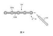
圖4為天線結構300的局部平面圖之一示例。在圖4繪示之垂直輻射體320中,垂直導體320A分別為圖3所示之垂直導體320A,而平面金屬結構320B為圖3所示之平面金屬結構320B中之一者。平面金屬結構320B的長度方向與水平輻射體330的長度方向之間的夾角θ為鈍角。如此一來,產生的輻射場型更可包含垂直於平面金屬結構320B之長度方向的水平極化分量。在其他實施例中,依據實際應用需求,平面金屬結構320B的長度方向與水平輻射體330的長度方向之間的夾角θ可變更為直角或銳角,或者平面金屬結構320B的長度方向可與水平輻射體330的長度方向平行。FIG. 4 is an example of a partial plan view of the
圖5為天線結構300的局部立體圖之一示例。在圖5繪示之垂直輻射體320中,垂直導體320A分別為圖3所示之垂直導體320A,而平面金屬結構320B為圖3所示之平面金屬結構320B中之上下相鄰二者。如圖5所示,在下層的平面金屬結構320B的缺口中更具有開關320C。在開關320C為導通狀態時,上下兩層的平面金屬結構320B均具有完整的電流路徑。相對地,在開關320C為關斷狀態時,上層的平面金屬結構320B仍具有完整的電流路徑,但下層的平面金屬結構320B不具有完整的電流路徑,因在開關320C兩側的金屬結構需經由垂直導體320A和上層的平面金屬結構320B(或圖5之上下兩層平面金屬結構320B之外的平面金屬結構)電性連接,而無法直接經由開關320C直接電性連接,使得垂直輻射體320的整體電流分佈因而改變。藉由切換開關320C的導通和關斷狀態,可改變垂直輻射體320的整體電流分佈,進而切換垂直輻射體320的輻射場型。FIG. 5 is an example of a partial perspective view of the
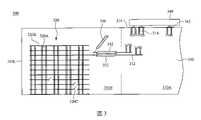
圖6為依據本發明另一些實施例之天線結構300'的示意圖。相較圖3之天線結構300,圖6之天線結構300'還包含金屬分支324,且在圖6中,開關320C耦接於金屬分支324與其中一個平面金屬結構320B之間,其用以控制金屬分支324與此平面金屬結構320B是否電性連接,且平面金屬結構320B中的開口均不具有開關320C。在天線結構300'中的其他元件分別與圖3之天線結構300中的對應元件相同,故相關說明請參照前述段落,在此不贅述。FIG. 6 is a schematic diagram of an
圖7為天線結構300'的局部平面圖之一示例。在圖7繪示之垂直輻射體320中,垂直導體320A分別為圖6所示之垂直導體320A,平面金屬結構320B為圖6所示之平面金屬結構320B中之一者,開關320C為圖7所示之開關320C,且金屬分支324為圖6所示之金屬分支324。FIG. 7 is an example of a partial plan view of an antenna structure 300' . In the
在圖7中,藉由控制開關320C的狀態,可決定分別在開關320C兩端的平面金屬結構320B和金屬分支324是否可經由開關320C電性連接。當開關320C導通時,平面金屬結構320B和金屬分支324經由開關320C電性連接,即在平面金屬結構320B中的電流部份流經金屬分支324。相對地,當開關320C關斷時,在開關320C兩側的金屬結構不直接經由開關320C電性連接,即阻斷垂直輻射體320中的電流流經開關320C。由於電流分佈決定垂直輻射體320產生的輻射場型,且金屬分支324的長度方向與平面金屬結構320B的長度方向不同,故經由控制開關320C導通和關斷狀態,可決定垂直輻射體320的天線增益和產生的輻射場型圖案,包含主波束方向、半功率波束寬、指向性和極化方向和指向性等。在圖7之實施例中,金屬分支324的長度方向與平面金屬結構320B的長度方向垂直。在其他實施例中,依據實際應用需求,金屬分支324的長度方向也可不與平面金屬結構320B的長度方向垂直。因此,藉由導通或關斷開關320C,可切換天線結構300'的輻射場型和極化狀態。In FIG. 7 , by controlling the state of the
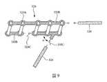
圖8為依據本發明另一些實施例之天線結構300"的示意圖。相較圖3之天線結構300和圖6之天線結構300',圖8之天線結構300"同時具有金屬分支324、位於平面金屬結構320B之缺口中的開關320C和位於平面金屬結構320B與金屬分支324之間的的開關320C。在天線結構300"中的元件分別與圖3之天線結構300和/或圖6之天線結構300'中的對應元件相同,故相關說明請參照前述段落,在此不贅述。8 is a schematic diagram of an
圖9為天線結構300"的局部立體圖之一示例。在圖9繪示之垂直輻射體320中,垂直導體320A分別為圖8所示之垂直導體320A,平面金屬結構320B分別為圖8所示之平面金屬結構320B中之上下相鄰二者,開關320C分別為圖8所示之開關320C中之二者,且金屬分支324為圖8所示之金屬分支324。圖9之在平面金屬結構320B之缺口中的開關320C和在平面金屬結構320B與金屬分支324之間的開關320C的作用分別與圖5和圖7之開關320C相同。此外,在圖9之實施例中,金屬分支324的長度方向與平面金屬結構320B的夾角Φ為銳角。在其他實施例中,依據實際應用需求,金屬分支324的長度方向與平面金屬結構320B的夾角Φ可以是直角或鈍角。因此,藉由導通或關斷每一開關320C,可切換天線結構300"的輻射場型和極化狀態。9 is an example of a partial perspective view of the
應注意的是,圖3至圖9所示之垂直導體320A、平面金屬結構320B、開關320C、及金屬分支324的圖案、位置和數量配置等僅為示例。在實際設計上,垂直導體320A、平面金屬結構320B、開關320C、及金屬分支324的圖案、位置和數量配置可依據應用需求對應調整,其不以為圖3至圖9所示之內容為限。It should be noted that the patterns, positions, and numbers of
綜上所述,本發明之天線結構具有輻射場型切換功能,其可依據所在環境切換其產生的輻射場型,故在不同環境下均可具有高傳輸和接收效能。To sum up, the antenna structure of the present invention has a radiation pattern switching function, which can switch the generated radiation pattern according to the environment, so that it can have high transmission and reception performance in different environments.
雖然本發明已以實施方式揭露如上,然其並非用以限定本發明,任何熟習此技藝者,在不脫離本發明之精神和範圍內,當可作各種之更動與潤飾,因此本發明之保護範圍當視後附之申請專利範圍所界定者為準。Although the present invention has been disclosed in the above embodiments, it is not intended to limit the present invention. Anyone skilled in the art can make various changes and modifications without departing from the spirit and scope of the present invention. Therefore, the protection of the present invention The scope shall be determined by the scope of the appended patent application.
300‧‧‧天線結構300‧‧‧Antenna Structure
310‧‧‧基板310‧‧‧Substrate
310A‧‧‧中央區310A‧‧‧Central District
310B‧‧‧邊緣區310B‧‧‧Edge Zone
310E‧‧‧側邊310E‧‧‧Side
312‧‧‧導線312‧‧‧Wire
314‧‧‧導孔結構314‧‧‧via structure
316‧‧‧接合墊316‧‧‧Bond pads
320‧‧‧垂直輻射體320‧‧‧Vertical Radiator
320A‧‧‧垂直導體320A‧‧‧Vertical Conductor
320B‧‧‧平面金屬結構320B‧‧‧Planar metal structure
320C‧‧‧開關320C‧‧‧Switch
322、332‧‧‧饋入線322, 332‧‧‧Feed-in line
330‧‧‧水平輻射體330‧‧‧Horizontal Radiator
340‧‧‧晶片340‧‧‧Chip
342‧‧‧金屬凸塊342‧‧‧Metal bumps
Claims (14)
Translated fromChineseApplications Claiming Priority (2)
| Application Number | Priority Date | Filing Date | Title |
|---|---|---|---|
| US16/219,918 | 2018-12-13 | ||
| US16/219,918US11588237B2 (en) | 2018-12-13 | 2018-12-13 | Antenna structure |
Publications (2)
| Publication Number | Publication Date |
|---|---|
| TW202023115A TW202023115A (en) | 2020-06-16 |
| TWI765132Btrue TWI765132B (en) | 2022-05-21 |
Family
ID=71072960
Family Applications (2)
| Application Number | Title | Priority Date | Filing Date |
|---|---|---|---|
| TW107147018ATWI765132B (en) | 2018-12-13 | 2018-12-25 | Antenna structure |
| TW111102958ATWI775709B (en) | 2018-12-13 | 2018-12-25 | Antenna structure |
Family Applications After (1)
| Application Number | Title | Priority Date | Filing Date |
|---|---|---|---|
| TW111102958ATWI775709B (en) | 2018-12-13 | 2018-12-25 | Antenna structure |
Country Status (3)
| Country | Link |
|---|---|
| US (2) | US11588237B2 (en) |
| CN (1) | CN111326850B (en) |
| TW (2) | TWI765132B (en) |
Families Citing this family (1)
| Publication number | Priority date | Publication date | Assignee | Title |
|---|---|---|---|---|
| KR102347788B1 (en)* | 2019-07-12 | 2022-01-06 | 주식회사 아모센스 | Ultra wide band antenna module |
Citations (3)
| Publication number | Priority date | Publication date | Assignee | Title |
|---|---|---|---|---|
| CN101496224A (en)* | 2006-07-28 | 2009-07-29 | 株式会社村田制作所 | Antenna device and radio communication device |
| US20150070231A1 (en)* | 2013-09-12 | 2015-03-12 | Korea Advanced Institute Of Science And Technology | Substrate embedded horn antenna having selection capability of vertical and horizontal radiation pattern |
| CN105449345A (en)* | 2014-09-19 | 2016-03-30 | 三星电子株式会社 | Antenna device and method for operation of the same |
Family Cites Families (14)
| Publication number | Priority date | Publication date | Assignee | Title |
|---|---|---|---|---|
| JP3843081B2 (en) | 2003-05-16 | 2006-11-08 | 株式会社インテリジェント・コスモス研究機構 | NRD guide converter |
| US7289064B2 (en)* | 2005-08-23 | 2007-10-30 | Intel Corporation | Compact multi-band, multi-port antenna |
| CN101114733B (en) | 2006-07-28 | 2011-04-20 | 连展科技电子(昆山)有限公司 | Integrated multi-frequency antenna with wide band function |
| US7760144B2 (en)* | 2008-08-04 | 2010-07-20 | Taiwan Semiconductor Manufacturing Company, Ltd. | Antennas integrated in semiconductor chips |
| US9270005B2 (en) | 2011-02-21 | 2016-02-23 | Siklu Communication ltd. | Laminate structures having a hole surrounding a probe for propagating millimeter waves |
| TW201405940A (en) | 2012-07-26 | 2014-02-01 | Univ Nat Taiwan | Substrate embedded antenna and antenna array constituted thereby |
| US9537208B2 (en) | 2012-11-12 | 2017-01-03 | Raytheon Company | Dual polarization current loop radiator with integrated balun |
| CN103606757B (en) | 2013-11-16 | 2016-05-25 | 华中科技大学 | A kind of dual-band dual-polarized antenna battle array |
| KR102138841B1 (en) | 2014-05-13 | 2020-08-11 | 삼성전자 주식회사 | Antenna device |
| EP3262711B1 (en) | 2015-02-26 | 2020-11-18 | The Government of the United States of America as represented by the Secretary of the Navy | Planar ultrawideband modular antenna array having improved bandwidth |
| CN106252878B (en) | 2016-08-04 | 2020-07-28 | 上海交通大学 | Space diversity covering transmitting-receiving system based on circularly polarized antenna |
| US9917365B1 (en) | 2016-08-31 | 2018-03-13 | Boise State University | Reconfigurable antennas for millimeter-wave systems that support multiple beams |
| CN108736160B (en) | 2017-04-20 | 2020-12-15 | 惠州硕贝德无线科技股份有限公司 | 5G terminal antenna with reconfigurable radiation pattern |
| CN108808237B (en) | 2018-06-28 | 2020-07-07 | 中国电子科技集团公司第十三研究所 | Planar omnidirectional circularly polarized antenna |
- 2018
- 2018-12-13USUS16/219,918patent/US11588237B2/enactiveActive
- 2018-12-25TWTW107147018Apatent/TWI765132B/enactive
- 2018-12-25TWTW111102958Apatent/TWI775709B/enactive
- 2018-12-25CNCN201811586655.6Apatent/CN111326850B/enactiveActive
- 2021
- 2021-11-16USUS17/455,206patent/US11658409B2/enactiveActive
Patent Citations (3)
| Publication number | Priority date | Publication date | Assignee | Title |
|---|---|---|---|---|
| CN101496224A (en)* | 2006-07-28 | 2009-07-29 | 株式会社村田制作所 | Antenna device and radio communication device |
| US20150070231A1 (en)* | 2013-09-12 | 2015-03-12 | Korea Advanced Institute Of Science And Technology | Substrate embedded horn antenna having selection capability of vertical and horizontal radiation pattern |
| CN105449345A (en)* | 2014-09-19 | 2016-03-30 | 三星电子株式会社 | Antenna device and method for operation of the same |
Also Published As
| Publication number | Publication date |
|---|---|
| TWI775709B (en) | 2022-08-21 |
| US20200194886A1 (en) | 2020-06-18 |
| US11658409B2 (en) | 2023-05-23 |
| CN111326850B (en) | 2022-07-22 |
| US20220077578A1 (en) | 2022-03-10 |
| CN111326850A (en) | 2020-06-23 |
| TW202023115A (en) | 2020-06-16 |
| TW202218245A (en) | 2022-05-01 |
| US11588237B2 (en) | 2023-02-21 |
Similar Documents
| Publication | Publication Date | Title |
|---|---|---|
| US11855353B2 (en) | Compact radio frequency (RF) communication modules with endfire and broadside antennas | |
| Patterson et al. | A 60-GHz active receiving switched-beam antenna array with integrated butler matrix and GaAs amplifiers | |
| CN100555747C (en) | The equipment and the method for structure and packaging printed antenna devices | |
| US10862211B2 (en) | Integrated antenna structure | |
| JP6964381B2 (en) | Wireless communication package with integrated antenna array | |
| US9985346B2 (en) | Wireless communications package with integrated antennas and air cavity | |
| JP6763087B2 (en) | Tiles for Active Electronically Scanned Array (AESA) | |
| CA2713353C (en) | Radio frequency (rf) integrated circuit (ic) packages with integrated aperture-coupled patch antenna(s) in ring and/or offset cavities | |
| US9305888B2 (en) | Integrated antenna structure and array | |
| US6556168B1 (en) | Phased array antenna and its manufacturing method | |
| CN103650132A (en) | Wireless module | |
| US20210043996A1 (en) | Thermal management method and apparatus for high frequency ic with apertured heat sink | |
| TWI765132B (en) | Antenna structure | |
| WO2000039893A1 (en) | Phased array antenna and its manufacturing method | |
| CN111446537B (en) | Antenna structure | |
| TWI819923B (en) | Antenna package structure | |
| JP2023182556A (en) | antenna package structure | |
| CN117239397A (en) | Antenna packaging structure | |
| CN120341569A (en) | Electronic Devices | |
| TW202435508A (en) | Millimeter wave embedded antenna |