TWI764447B - Buck-boost converter and control method - Google Patents
Buck-boost converter and control methodInfo
- Publication number
- TWI764447B TWI764447BTW109144807ATW109144807ATWI764447BTW I764447 BTWI764447 BTW I764447BTW 109144807 ATW109144807 ATW 109144807ATW 109144807 ATW109144807 ATW 109144807ATW I764447 BTWI764447 BTW I764447B
- Authority
- TW
- Taiwan
- Prior art keywords
- buck
- boost converter
- voltage
- input
- current
- Prior art date
Links
Images


Classifications
- H—ELECTRICITY
- H02—GENERATION; CONVERSION OR DISTRIBUTION OF ELECTRIC POWER
- H02M—APPARATUS FOR CONVERSION BETWEEN AC AND AC, BETWEEN AC AND DC, OR BETWEEN DC AND DC, AND FOR USE WITH MAINS OR SIMILAR POWER SUPPLY SYSTEMS; CONVERSION OF DC OR AC INPUT POWER INTO SURGE OUTPUT POWER; CONTROL OR REGULATION THEREOF
- H02M3/00—Conversion of DC power input into DC power output
- H02M3/02—Conversion of DC power input into DC power output without intermediate conversion into AC
- H02M3/04—Conversion of DC power input into DC power output without intermediate conversion into AC by static converters
- H02M3/10—Conversion of DC power input into DC power output without intermediate conversion into AC by static converters using discharge tubes with control electrode or semiconductor devices with control electrode
- H02M3/145—Conversion of DC power input into DC power output without intermediate conversion into AC by static converters using discharge tubes with control electrode or semiconductor devices with control electrode using devices of a triode or transistor type requiring continuous application of a control signal
- H02M3/155—Conversion of DC power input into DC power output without intermediate conversion into AC by static converters using discharge tubes with control electrode or semiconductor devices with control electrode using devices of a triode or transistor type requiring continuous application of a control signal using semiconductor devices only
- H02M3/156—Conversion of DC power input into DC power output without intermediate conversion into AC by static converters using discharge tubes with control electrode or semiconductor devices with control electrode using devices of a triode or transistor type requiring continuous application of a control signal using semiconductor devices only with automatic control of output voltage or current, e.g. switching regulators
- H02M3/158—Conversion of DC power input into DC power output without intermediate conversion into AC by static converters using discharge tubes with control electrode or semiconductor devices with control electrode using devices of a triode or transistor type requiring continuous application of a control signal using semiconductor devices only with automatic control of output voltage or current, e.g. switching regulators including plural semiconductor devices as final control devices for a single load
- H02M3/1582—Buck-boost converters
- H—ELECTRICITY
- H02—GENERATION; CONVERSION OR DISTRIBUTION OF ELECTRIC POWER
- H02M—APPARATUS FOR CONVERSION BETWEEN AC AND AC, BETWEEN AC AND DC, OR BETWEEN DC AND DC, AND FOR USE WITH MAINS OR SIMILAR POWER SUPPLY SYSTEMS; CONVERSION OF DC OR AC INPUT POWER INTO SURGE OUTPUT POWER; CONTROL OR REGULATION THEREOF
- H02M1/00—Details of apparatus for conversion
- H02M1/0003—Details of control, feedback or regulation circuits
- H02M1/0025—Arrangements for modifying reference values, feedback values or error values in the control loop of a converter
- H—ELECTRICITY
- H02—GENERATION; CONVERSION OR DISTRIBUTION OF ELECTRIC POWER
- H02M—APPARATUS FOR CONVERSION BETWEEN AC AND AC, BETWEEN AC AND DC, OR BETWEEN DC AND DC, AND FOR USE WITH MAINS OR SIMILAR POWER SUPPLY SYSTEMS; CONVERSION OF DC OR AC INPUT POWER INTO SURGE OUTPUT POWER; CONTROL OR REGULATION THEREOF
- H02M1/00—Details of apparatus for conversion
- H02M1/08—Circuits specially adapted for the generation of control voltages for semiconductor devices incorporated in static converters
- H02M1/088—Circuits specially adapted for the generation of control voltages for semiconductor devices incorporated in static converters for the simultaneous control of series or parallel connected semiconductor devices
- H—ELECTRICITY
- H02—GENERATION; CONVERSION OR DISTRIBUTION OF ELECTRIC POWER
- H02M—APPARATUS FOR CONVERSION BETWEEN AC AND AC, BETWEEN AC AND DC, OR BETWEEN DC AND DC, AND FOR USE WITH MAINS OR SIMILAR POWER SUPPLY SYSTEMS; CONVERSION OF DC OR AC INPUT POWER INTO SURGE OUTPUT POWER; CONTROL OR REGULATION THEREOF
- H02M1/00—Details of apparatus for conversion
- H02M1/38—Means for preventing simultaneous conduction of switches
- H—ELECTRICITY
- H02—GENERATION; CONVERSION OR DISTRIBUTION OF ELECTRIC POWER
- H02M—APPARATUS FOR CONVERSION BETWEEN AC AND AC, BETWEEN AC AND DC, OR BETWEEN DC AND DC, AND FOR USE WITH MAINS OR SIMILAR POWER SUPPLY SYSTEMS; CONVERSION OF DC OR AC INPUT POWER INTO SURGE OUTPUT POWER; CONTROL OR REGULATION THEREOF
- H02M3/00—Conversion of DC power input into DC power output
- H02M3/02—Conversion of DC power input into DC power output without intermediate conversion into AC
- H02M3/04—Conversion of DC power input into DC power output without intermediate conversion into AC by static converters
- H02M3/10—Conversion of DC power input into DC power output without intermediate conversion into AC by static converters using discharge tubes with control electrode or semiconductor devices with control electrode
- H02M3/145—Conversion of DC power input into DC power output without intermediate conversion into AC by static converters using discharge tubes with control electrode or semiconductor devices with control electrode using devices of a triode or transistor type requiring continuous application of a control signal
- H02M3/155—Conversion of DC power input into DC power output without intermediate conversion into AC by static converters using discharge tubes with control electrode or semiconductor devices with control electrode using devices of a triode or transistor type requiring continuous application of a control signal using semiconductor devices only
- H02M3/156—Conversion of DC power input into DC power output without intermediate conversion into AC by static converters using discharge tubes with control electrode or semiconductor devices with control electrode using devices of a triode or transistor type requiring continuous application of a control signal using semiconductor devices only with automatic control of output voltage or current, e.g. switching regulators
- H02M3/157—Conversion of DC power input into DC power output without intermediate conversion into AC by static converters using discharge tubes with control electrode or semiconductor devices with control electrode using devices of a triode or transistor type requiring continuous application of a control signal using semiconductor devices only with automatic control of output voltage or current, e.g. switching regulators with digital control
- H—ELECTRICITY
- H02—GENERATION; CONVERSION OR DISTRIBUTION OF ELECTRIC POWER
- H02M—APPARATUS FOR CONVERSION BETWEEN AC AND AC, BETWEEN AC AND DC, OR BETWEEN DC AND DC, AND FOR USE WITH MAINS OR SIMILAR POWER SUPPLY SYSTEMS; CONVERSION OF DC OR AC INPUT POWER INTO SURGE OUTPUT POWER; CONTROL OR REGULATION THEREOF
- H02M1/00—Details of apparatus for conversion
- H02M1/0003—Details of control, feedback or regulation circuits
- H02M1/0009—Devices or circuits for detecting current in a converter
- H—ELECTRICITY
- H02—GENERATION; CONVERSION OR DISTRIBUTION OF ELECTRIC POWER
- H02M—APPARATUS FOR CONVERSION BETWEEN AC AND AC, BETWEEN AC AND DC, OR BETWEEN DC AND DC, AND FOR USE WITH MAINS OR SIMILAR POWER SUPPLY SYSTEMS; CONVERSION OF DC OR AC INPUT POWER INTO SURGE OUTPUT POWER; CONTROL OR REGULATION THEREOF
- H02M1/00—Details of apparatus for conversion
- H02M1/0003—Details of control, feedback or regulation circuits
- H02M1/0016—Control circuits providing compensation of output voltage deviations using feedforward of disturbance parameters
- H02M1/0022—Control circuits providing compensation of output voltage deviations using feedforward of disturbance parameters the disturbance parameters being input voltage fluctuations
Landscapes
- Engineering & Computer Science (AREA)
- Power Engineering (AREA)
- Dc-Dc Converters (AREA)
Abstract
Description
Translated fromChinese本發明涉及功率轉換器的控制方案,並且在特定實施例中,涉及在各種操作狀况下採用具有恆定開關頻率的恆定導通時間控制方案的功率轉換器。The present invention relates to control schemes for power converters and, in particular embodiments, to power converters that employ a constant on-time control scheme with constant switching frequency under various operating conditions.
隨著技術進一步發展,諸如移動電話、平板PC、數碼相機、MP3播放器和/或類似裝置的各種電子裝置變得普及。每個電子裝置都需要大體上恆定電壓的直流功率,其電壓甚至在由電子裝置汲取的電流可在較寬範圍內變化時也可在指定誤差內進行調節。為了使電壓維持在指定公差內,耦合到電子裝置的功率轉換器(例如,開關式dc/dc轉換器)提供非常快速的瞬態響應,同時在各種負載瞬變下保持穩定的輸出電壓。As technology further develops, various electronic devices such as mobile phones, tablet PCs, digital cameras, MP3 players and/or similar devices have become popular. Every electronic device requires a substantially constant voltage DC power, the voltage of which can be adjusted within specified tolerances even when the current drawn by the electronic device can vary over a wide range. To maintain voltage within specified tolerances, power converters (eg, switching dc/dc converters) coupled to electronic devices provide very fast transient response while maintaining a stable output voltage under various load transients.
諸如恆定導通時間方案或恆定關斷時間方案的基於滯後的功率轉換器控制方案可使得功率轉換器能夠提供快速瞬態響應。採用恆定導通時間控制方案的功率轉換器可只包括反饋比較器和導通計時器。在操作中,功率轉換器的反饋電路將反饋信號與內部參考直接進行比較。當反饋信號下降至低於內部參考時,功率轉換器的高側開關打開,並且在導通計時器時間內保持接通狀態。作為打開高側開關的結果,功率轉換器的電感電流上升。當導通計時器到期時,功率轉換器的高側開關關閉,並且直到反饋信號再次下降至低於內部參考時才打開。總之,當在功率轉換器中採用恆定導通時間控制方案時,通過導通計時器來終止功率轉換器的高側開關的導通時間。通過反饋比較器來終止功率轉換器的高側開關的關斷時間。A hysteresis-based power converter control scheme, such as a constant on-time scheme or a constant off-time scheme, can enable the power converter to provide fast transient response. A power converter employing a constant on-time control scheme may only include a feedback comparator and an on-timer. In operation, the feedback circuit of the power converter directly compares the feedback signal to an internal reference. When the feedback signal falls below the internal reference, the high-side switch of the power converter turns on and remains on for the on-timer time. As a result of turning on the high-side switch, the inductor current of the power converter rises. When the on-timer expires, the high-side switch of the power converter turns off and does not turn on until the feedback signal drops below the internal reference again. In summary, when a constant on-time control scheme is employed in a power converter, the on-time of the high-side switch of the power converter is terminated by an on-timer. The off-time of the high-side switch of the power converter is terminated by a feedback comparator.
隨著電子裝置朝向便攜式和移動式發展,許多電子裝置依賴於可充電電池作為它們的電源。然而,由於可充電電池的特性,電池組的輸出電壓可能會在充滿電的狀態和完全耗盡的狀態之間的廣泛範圍內變化。另外,隨著C型通用串行總線(USB)作為充電和傳遞數據的新標準出現,USB端口的輸出電壓不再固定(例如,5V)。而是,輸出電壓可在從約3.5V到約20V的廣泛範圍內變化。與此同時,連接到新型USB端口(例如,C型USB)的下游功率轉換器可能仍然需要大體上約為5V的電壓。響應於廣泛的輸入電壓範圍,對於C型USB應用,四開關降壓-升壓式轉換器變得普遍存在。As electronic devices become portable and mobile, many electronic devices rely on rechargeable batteries as their power source. However, due to the characteristics of rechargeable batteries, the output voltage of the battery pack may vary widely between a fully charged state and a fully depleted state. Also, with the emergence of Universal Serial Bus Type-C (USB) as the new standard for charging and transferring data, the output voltage of a USB port is no longer fixed (eg, 5V). Rather, the output voltage can vary widely from about 3.5V to about 20V. At the same time, downstream power converters connected to newer USB ports (eg, USB Type-C) may still require roughly 5V. In response to the wide input voltage range, four-switch buck-boost converters have become ubiquitous for USB Type-C applications.
在傳統的四開關降壓-升壓式轉換器中,在每個開關循環中,一次打開和關閉所有四個開關。另外,從不將輸入電源的能量直接傳遞到四開關降壓-升壓式轉換器的輸出端。而是,首先將輸入電源的能量儲存在降壓-升壓式轉換器的電感中,然後再傳遞到轉換器的輸出端。因此,傳統的四開關降壓-升壓式轉換器的效率不高。In a conventional four-switch buck-boost converter, in each switching cycle, all four switches are turned on and off at once. In addition, the energy of the input power supply is never delivered directly to the output of the four-switch buck-boost converter. Instead, the energy of the input power supply is first stored in the buck-boost converter's inductor before being delivered to the converter's output. Therefore, the traditional four-switch buck-boost converter is not very efficient.
可取的是提供用於使得採用恆定導通時間控制方案的傳統的四開關降壓-升壓式轉換器能夠在不同的輸入電壓下以降壓模式、升壓模式和降壓-升壓模式操作的設備和/或方法。此外,可取的是響應於輸入電壓變化在以上任意兩種操作模式之間具有平穩的轉變。It is desirable to provide apparatus for enabling a conventional four-switch buck-boost converter employing a constant on-time control scheme to operate in buck mode, boost mode and buck-boost mode at different input voltages and/or method. Furthermore, it is desirable to have a smooth transition between any of the above two modes of operation in response to input voltage changes.
在特定實施例中,一種控制方案可在各種操作狀况下實現快速瞬態響應並提高四開關降壓-升壓式轉換器的性能。In certain embodiments, a control scheme can achieve fast transient response and improve the performance of a four-switch buck-boost converter under various operating conditions.
根據一個實施例,一種設備包括:第一計時器,第一計時器配置成確定對降壓-升壓式轉換器的降壓轉換器部分的高側開關施加的栅極驅動信號的關閉沿,其中第一計時器包括配置成接收第一斜坡信號的第一輸入端和配置成接收第一閾值電壓的第二輸入端,並且其中第一斜坡信號由具有與降壓-升壓式轉換器的輸入電壓成比例的電流電平的第一電流源生成,並且第一閾值電壓與降壓-升壓式轉換器的輸出電壓成比例;以及第二計時器,第二計時器被配置成確定對降壓-升壓式轉換器的升壓轉換器部分的低側開關施加的栅極驅動信號的關閉沿,其中第二計時器包括配置成接收第二斜坡信號的第一輸入端和配置成接收第二閾值電壓的第二輸入端,並且其中第二斜坡信號由具有與降壓-升壓式轉換器的輸出電壓成比例的電流電平的第二電流源生成,並且第二閾值電壓與降壓-升壓式轉換器的輸出電壓和降壓-升壓式轉換器的輸入電壓之間的差成比例。According to one embodiment, an apparatus includes a first timer configured to determine an off edge of a gate drive signal applied to a high-side switch of a buck converter portion of a buck-boost converter, wherein the first timer includes a first input configured to receive a first ramp signal and a second input configured to receive a first threshold voltage, and wherein the first ramp signal is provided by a buck-boost converter having a a first current source generating a current level proportional to the input voltage and a first threshold voltage proportional to the output voltage of the buck-boost converter; and a second timer configured to determine a pair of an off edge of a gate drive signal applied by a low-side switch of a boost converter portion of a buck-boost converter, wherein the second timer includes a first input configured to receive the second ramp signal and configured to receive a second input of a second threshold voltage, and wherein the second ramp signal is generated by a second current source having a current level proportional to the output voltage of the buck-boost converter, and wherein the second threshold voltage is proportional to the drop The difference between the output voltage of the buck-boost converter and the input voltage of the buck-boost converter is proportional.
根據另一個實施例,一種方法包括:利用具有與降壓-升壓式轉換器的輸入電壓成比例的電流電平的第一電流源生成第一斜坡信號;利用具有與降壓-升壓式轉換器的輸出電壓成比例的電流電平的第二電流源生成第二斜坡信號;生成與降壓-升壓式轉換器的輸出電壓成比例的第一閾值電壓;生成與降壓-升壓式轉換器的輸出電壓和輸入電壓之間的差成比例的第二閾值電壓;利用第一比較器比較第一閾值電壓與第一斜坡信號和第一預設偏移電壓的總和;利用第二比較器比較第二閾值電壓與第二斜坡信號和第二預設偏移電壓的總和;基於由第一比較器生成的比較結果終止降壓-升壓式轉換器的降壓轉換器部分的高側開關的栅極驅動信號;以及基於由第二比較器生成的比較結果終止降壓-升壓式轉換器的升壓轉換器部分的低側開關的栅極驅動信號。According to another embodiment, a method includes generating a first ramp signal with a first current source having a current level proportional to an input voltage of a buck-boost converter; a second current source of a current level proportional to the output voltage of the converter generates a second ramp signal; generates a first threshold voltage proportional to the output voltage of the buck-boost converter; generates a buck-boost a second threshold voltage proportional to the difference between the output voltage and the input voltage of the converter; using the first comparator to compare the first threshold voltage with the sum of the first ramp signal and the first preset offset voltage; using the second A comparator compares the second threshold voltage to a sum of the second ramp signal and the second preset offset voltage; terminating high of the buck converter portion of the buck-boost converter based on the result of the comparison generated by the first comparator a gate drive signal for the side switch; and a gate drive signal for terminating the low side switch of the boost converter portion of the buck-boost converter based on the result of the comparison generated by the second comparator.
根據又一個實施例,一種控制器包括:用於設置降壓-升壓式轉換器的第一高側開關的打開時間的第一計時器,其中通過降壓-升壓式轉換器的輸入電壓、降壓-升壓式轉換器的輸出電壓和第一預設偏置電壓確定第一高側開關的打開時間;用於設置降壓-升壓式轉換器的第二低側開關的打開時間的第二計時器,其中通過降壓-升壓式轉換器的輸入電壓、降壓-升壓式轉換器的輸出電壓和第二預設偏置電壓確定第二低側開關的打開時間;以及用於設置降壓-升壓式轉換器的第一低側開關的打開時間和第二高側開關的打開時間的谷值電流模式控制裝置。According to yet another embodiment, a controller includes a first timer for setting an on-time of a first high-side switch of a buck-boost converter, wherein an input voltage of the buck-boost converter is passed through , the output voltage of the buck-boost converter and the first preset bias voltage determine the turn-on time of the first high-side switch; used to set the turn-on time of the second low-side switch of the buck-boost converter the second timer, wherein the turn-on time of the second low-side switch is determined by the input voltage of the buck-boost converter, the output voltage of the buck-boost converter, and a second preset bias voltage; and A valley current mode control means for setting the turn-on time of the first low-side switch and the turn-on time of the second high-side switch of the buck-boost converter.
本公開的較佳實施例的優點是提高降壓-升壓式功率轉換器的性能。更具體地,降壓-升壓式轉換器的控制機制基於恆定導通時間(COnT)谷值電流模式(VCM)控制。恆定導通時間控制消除了對固定時鐘信號的需要。此外,利用恆定導通時間控制,可自動實現從脉衝寬度調製(PWM)模式到脉衝頻率調製(PFM)模式的轉變。而且,可消除峰值電流模式(PCM)控制所需的斜率補償。恆定導通時間控制可大大簡化控制電路和相關聯的電流消耗。利用谷值電流模式控制,由電感和輸出電容形成的輸出雙極可縮減為單極響應,從而使控制回路補償設計簡單得多。An advantage of the preferred embodiments of the present disclosure is to improve the performance of a buck-boost power converter. More specifically, the control mechanism of the buck-boost converter is based on constant on-time (COnT) valley current mode (VCM) control. Constant on-time control eliminates the need for a fixed clock signal. Additionally, with constant on-time control, the transition from Pulse Width Modulation (PWM) mode to Pulse Frequency Modulation (PFM) mode is automated. Also, slope compensation required for peak current mode (PCM) control can be eliminated. Constant on-time control greatly simplifies the control circuitry and associated current consumption. With valley current mode control, the output bipolar formed by the inductor and output capacitor can be reduced to a unipolar response, making the control loop compensation design much simpler.
上文相當廣泛地概述了本發明的特徵和技術優點,以便可以更好地瞭解以下對本發明的詳細描述。下文將描述形成本發明的請求項的主題的本發明的額外特徵和優點。本領域技術人員應明白,可容易地利用公開的概念和特定實施例作為修改或設計用於實現本發明的相同目的的其它結構或過程的基礎。本領域技術人員還應意識到,此類等效構造並未偏離隨附請求項中闡述的本發明的精神和範圍。The foregoing has outlined rather broadly the features and technical advantages of the present invention in order that the detailed description of the invention that follows may be better understood. Additional features and advantages of the invention will be described hereinafter which form the subject of the claimed invention. It should be appreciated by those skilled in the art that the conception and specific embodiment disclosed may be readily utilized as a basis for modifying or designing other structures or processes for carrying out the same purposes of the present invention. Those skilled in the art should also realize that such equivalent constructions do not depart from the spirit and scope of the invention as set forth in the appended claims.
除非另外指示,否則不同圖中的對應數字和符號一般指對應部分。繪製附圖是為了清楚地說明各種實施例的相關方面,附圖不一定按比例繪製。Corresponding numerals and symbols in the different figures generally refer to corresponding parts unless otherwise indicated. The drawings are drawn to clearly illustrate relevant aspects of the various embodiments and are not necessarily drawn to scale.
下文詳細論述目前較佳的實施例的製作和使用。但是,應明白,本發明提供可在各種各樣的特定背景中實施的許多適用的發明概念。論述的特定實施例只是說明製作和使用本公開的特定方式,而不是限制本公開的範圍。The making and using of the presently preferred embodiments are discussed in detail below. It should be appreciated, however, that the present invention provides many applicable inventive concepts that can be embodied in a wide variety of specific contexts. The specific embodiments discussed are merely illustrative of specific ways to make and use the disclosure, and do not limit the scope of the disclosure.
將在特定背景、即在各種操作狀况下以固定開關頻率或幾乎固定的開關頻率操作的恆定導通時間控制的功率轉換器中關於較佳實施例描述本公開。然而,本發明也可適用於各種功率轉換器。在下文中,將參考附圖詳細解釋各種實施例。The present disclosure will be described with respect to preferred embodiments in the specific context of a constant on-time controlled power converter operating at a fixed or nearly fixed switching frequency under various operating conditions. However, the present invention is also applicable to various power converters. Hereinafter, various embodiments will be explained in detail with reference to the accompanying drawings.
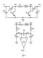
圖1示出根據本公開的各種實施例的降壓-升壓式轉換器及其相關聯的恆定導通時間控制電路的示意圖。如圖1所示,降壓-升壓式轉換器包括第一高側開關Q1、第一低側開關Q2、第二低側開關Q3、第二高側開關Q4和電感204。第一高側開關Q1和第一低側開關Q2串聯連接在輸入電容201的正極端子和負極端子之間。輸入電容201連接到電源VIN。採用輸入電容201來為降壓-升壓式轉換器提供穩定電壓。第二高側開關Q4和第二低側開關Q3串聯連接在輸出電容207的正極端子和負極端子之間。電感204耦合在第一高側開關Q1和第一低側開關Q2的公共節點與第二高側開關Q4和第二低側開關Q3的公共節點之間。1 shows a schematic diagram of a buck-boost converter and its associated constant on-time control circuit according to various embodiments of the present disclosure. As shown in FIG. 1 , the buck-boost converter includes a first high-side switch Q1 , a first low-side switch Q2 , a second low-side switch Q3 , a second high-side switch Q4 and an
降壓-升壓式轉換器可劃分成兩個部分,即降壓轉換器部分和升壓轉換器部分。降壓轉換器部分可包括第一高側開關Q1和第一低側開關Q2。降壓轉換器部分和電感204可充當降壓型轉換器。另一方面,升壓轉換器部分可包括第二高側開關Q4和第二低側開關Q3。升壓轉換器部分和電感204可充當升壓型轉換器。降壓轉換器部分、電感204和升壓轉換器部分級聯連接在輸入電容201和輸出電容207之間。A buck-boost converter can be divided into two parts, a buck converter part and a boost converter part. The buck converter portion may include a first high-side switch Q1 and a first low-side switch Q2. The buck converter section and the
降壓-升壓式轉換器的降壓轉換器部分和升壓轉換器部分均由恆定導通時間控制電路控制。如圖1所示,恆定導通時間控制電路包括放大器218、谷值電流比較器214、降壓導通時間計時器230、升壓導通時間計時器240、第一鎖存器211、第二鎖存器219、降壓控制邏輯單元210和升壓控制邏輯單元212。Both the buck converter portion and the boost converter portion of the buck-boost converter are controlled by a constant on-time control circuit. As shown in FIG. 1 , the constant on-time control circuit includes an
如圖1所示,恆定導通時間控制電路可檢測輸出電壓VOUT和流過電感204的電流,並相應地生成用於驅動開關Q1、Q2、Q3和Q4的多個栅極驅動信號。As shown in FIG. 1 , the constant on-time control circuit can sense the output voltage VOUT and the current flowing through the
在一些實施例中,放大器218是電壓誤差放大器。如圖1所示,放大器218的反相輸入端(FB)用於通過由電阻208和209形成的分壓器檢測輸出電壓VOUT。放大器218的同相輸入端連接到預設參考電壓VREF。放大器218的輸出端連接到谷值電流比較器214的同相輸入端。補償網路連接在放大器218的輸出端和地之間。補償網路包括電阻215、電容216和電容217。電阻215與電容216串聯連接,並且進一步與電容217並聯連接。補償網路有助於穩定控制回路並提供足夠的相位裕量,從而提高降壓-升壓式轉換器的瞬態響應性能。In some embodiments,
谷值電流比較器214的反相輸入端被配置成接收檢測的電流信號(CS)。如圖1所示,通過合適的電流感應裝置來檢測流過電感204的電流,例如直流電阻(DCR)電流感應設備。通過電流感應放大器213將感應的電流信號饋送到谷值電流比較器214的反相輸入端。採用電流感應放大器213來提供合適的電流感應增益。The inverting input of valley
採用第一鎖存器211來分別為開關Q1和Q2生成栅極驅動信號。如圖1所示,第一鎖存器211的復位輸入端配置成接收降壓導通時間計時器230的輸出信號。第一鎖存器211的設置輸入端配置成接收谷值電流比較器214的輸出信號。第一鎖存器211的輸出是用於控制降壓-升壓式轉換器的降壓轉換器部分的PWM信號。如圖1所示,通過降壓控制邏輯單元210將第一鎖存器211的輸出分別施加到開關Q1和Q2的栅極。採用降壓控制邏輯單元210來基於由第一鎖存器211生成的PWM信號生成高壓側栅極驅動信號和低壓側栅極驅動信號。此外,降壓控制邏輯單元210在高壓側栅極驅動信號和低壓側栅極驅動信號之間增加適當的延遲。降壓導通時間計時器230的詳細示意圖將在下文中的圖2進行描述。A
採用第二鎖存器219來分別為開關Q3和Q4生成栅極驅動信號。如圖1所示,第二鎖存器219的復位輸入端配置成接收升壓導通時間計時器240的輸出信號。第二鎖存器219的設置輸入端配置成接收谷值電流比較器214的輸出信號。第二鎖存器219的輸出是用於控制降壓-升壓式轉換器的升壓轉換器部分的PWM信號。如圖1所示,通過升壓控制邏輯單元212將第二鎖存器219的輸出分別施加到開關Q3和Q4的栅極。採用升壓控制邏輯單元212來基於由第二鎖存器219生成的PWM信號生成高壓側栅極驅動信號和低壓側栅極驅動信號。此外,升壓控制邏輯單元212在高壓側栅極驅動信號和低壓側栅極驅動信號之間增加適當的延遲。下文將參照圖2描述升壓導通時間計時器240的詳細示意圖。A
應注意,儘管本描述通篇中的示例基於降壓-升壓式轉換器和配置成為降壓-升壓式轉換器(例如,如圖1所示的降壓-升壓式轉換器)生成栅極驅動信號的恆定導通時間控制電路,但是如圖1所示的降壓-升壓式轉換器和恆定導通時間控制電路可具有許多改變、備選和修改。例如,恆定導通時間控制電路可檢測其它必需的信號,如降壓-升壓式轉換器的輸入電壓、輸入電流和/或輸出電流。此外,可以有一個專用驅動器或多個專用驅動器耦合在恆定導通時間控制電路與開關Q1、Q2、Q3和Q4之間。總之,限制本文中說明的降壓-升壓式轉換器和恆定導通時間控制電路只是為了清楚地說明各種實施例的發明方面。本公開不限於任何特定的功率拓撲和系統配置。It should be noted that although the examples throughout this description are based on a buck-boost converter and are configured to generate a buck-boost converter (eg, as shown in Figure 1) A constant on-time control circuit for the gate drive signal, but the buck-boost converter and constant on-time control circuit shown in Figure 1 can have many variations, alternatives and modifications. For example, the constant on-time control circuit may detect other necessary signals, such as the input voltage, input current and/or output current of the buck-boost converter. Additionally, there may be a dedicated driver or multiple dedicated drivers coupled between the constant on-time control circuit and switches Q1, Q2, Q3 and Q4. In conclusion, the buck-boost converters and constant on-time control circuits described herein are limited only to clearly illustrate the inventive aspects of the various embodiments. The present disclosure is not limited to any particular power topology and system configuration.
圖1中示出的開關(例如,第一高側開關Q1)可作為n-型金屬氧化物半導體(NMOS)晶體管實現。在另一些實施例中,這些開關可作為其它合適的可控裝置實現,如金屬氧化物半導體場效應晶體管(MOSFET)裝置、雙極結型晶體管(BJT)裝置、超級結型晶體管(SJT)裝置、絕緣栅雙極晶體管(IGBT)裝置、基於氮化鎵(GaN)的功率裝置和/或類似裝置。The switches shown in FIG. 1 (eg, the first high-side switch Q1 ) may be implemented as n-type metal oxide semiconductor (NMOS) transistors. In other embodiments, these switches may be implemented as other suitable controllable devices, such as metal oxide semiconductor field effect transistor (MOSFET) devices, bipolar junction transistor (BJT) devices, super junction transistor (SJT) devices , Insulated Gate Bipolar Transistor (IGBT) devices, Gallium Nitride (GaN) based power devices and/or similar devices.
還應注意,儘管圖1示出四個開關Q1、Q2、Q3和Q4,但是本公開的各種實施例可包括其它改變、修改和備選。例如,可通過續流二極管和/或類似組件來取代低側開關Q2。可通過整流二極管和/或類似組件來取代高側開關Q4。It should also be noted that although FIG. 1 shows four switches Q1 , Q2 , Q3 and Q4 , various embodiments of the present disclosure may include other changes, modifications and alternatives. For example, the low-side switch Q2 may be replaced by a freewheeling diode and/or similar components. The high-side switch Q4 can be replaced by a rectifier diode and/or similar components.
基於不同設計需要和應用,降壓-升壓式轉換器可配置成以三種不同的操作模式、即降壓操作模式、升壓操作模式和降壓-升壓操作模式操作。下文將分別參照圖3至圖5描述這三種操作模式的詳細操作原理。Based on different design needs and applications, a buck-boost converter can be configured to operate in three different modes of operation, namely a buck mode of operation, a boost mode of operation, and a buck-boost mode of operation. The detailed operation principles of the three operation modes will be described below with reference to FIGS. 3 to 5 , respectively.
在一些實施例中,降壓-升壓式轉換器配置成以降壓操作模式操作。在降壓操作模式中,採用與傳統的降壓轉換器中相同的方式來控制開關Q1和Q2,即通過具有合適的開關死區時間的互補栅極驅動信號來控制開關Q1和Q2。開關Q3始終關閉,並且開關Q4始終打開。下文將參照圖3描述降壓操作模式的詳細操作原理。In some embodiments, the buck-boost converter is configured to operate in a buck mode of operation. In the buck mode of operation, switches Q1 and Q2 are controlled in the same way as in conventional buck converters, ie by complementary gate drive signals with suitable switching deadtimes. Switch Q3 is always closed and switch Q4 is always open. The detailed operation principle of the buck operation mode will be described below with reference to FIG. 3 .
在一些實施例中,降壓-升壓式轉換器配置成以降壓-升壓操作模式操作。在降壓-升壓操作模式中,採用與傳統的降壓轉換器中相同的方式來控制開關Q1和Q2,即通過具有合適的開關死區時間的互補栅極驅動信號來控制開關Q1和Q2。採用與傳統的升壓轉換器中相同的方式來控制開關Q3和Q4,即通過具有合適的開關死區時間的互補栅極驅動信號來控制開關Q3和Q4。下文將參照圖4描述第二種控制機制的詳細操作原理。In some embodiments, the buck-boost converter is configured to operate in a buck-boost mode of operation. In the buck-boost mode of operation, switches Q1 and Q2 are controlled in the same way as in conventional buck converters, ie by complementary gate drive signals with suitable switch deadtimes . Switches Q3 and Q4 are controlled in the same way as in a conventional boost converter, ie by complementary gate drive signals with suitable switching deadtimes. The detailed operating principle of the second control mechanism will be described below with reference to FIG. 4 .
在一些實施例中,降壓-升壓式轉換器配置成以升壓操作模式操作。在升壓操作模式中,採用與傳統的升壓轉換器中相同的方式通來控制開關Q3和Q4,即通過具有合適的開關死區時間的互補栅極驅動信號來控制開關Q3和Q4。開關Q2始終關閉,並且開關Q1始終打開。下文將參照圖5描述升壓操作模式的詳細操作原理。In some embodiments, the buck-boost converter is configured to operate in a boost mode of operation. In the boost mode of operation, switches Q3 and Q4 are controlled in the same way as in a conventional boost converter, ie by complementary gate drive signals with suitable switch deadtimes. Switch Q2 is always closed and switch Q1 is always open. The detailed operation principle of the boost operation mode will be described below with reference to FIG. 5 .
圖2示出根據本公開的各種實施例的降壓導通時間計時器和升壓導通時間計時器的示意圖。在一些實施例中,降壓導通時間計時器230配置成計算降壓轉換器部分的導通時間,並且升壓導通時間計時器240配置成計算升壓轉換器部分的導通時間。2 shows a schematic diagram of a buck on-time timer and a boost on-time timer in accordance with various embodiments of the present disclosure. In some embodiments, the buck on-
如圖2所示,降壓導通時間計時器230包括電流源303、電容304、開關305、比較器301、“或”門306、反相器307和降壓偏置電壓源302。如圖2所示,電流源303的電流電平與輸入電壓VIN成比例。在一些實施例中,k2是預設係數。利用電流源303來對電容304充電。電容304兩端的電壓是電壓斜坡信號。在通篇描述中,電容304也可稱為斜坡信號電容。As shown in FIG. 2 , the buck on-
降壓偏置電壓源302與電容304串聯連接。如圖2所示,降壓偏置電壓源302的負極端子連接到電容304的第一端子。電容304的第二端子接地。將電容304兩端的電壓和降壓偏置電壓源302的總和饋送到比較器301的同相輸入端。比較器301的反相輸入端連接到閾值電壓,該閾值電壓與輸出電壓成比例。在一些實施例中,k1是預設係數。通過“或”門306的輸出信號控制開關305的栅極。如圖2所示,“或”門306配置成通過反相器307接收由第一鎖存器211生成的PWM信號以及接收由谷值電流比較器214生成的CMP信號。如圖2所示,PWM和CMP信號的組合確定電容304的復位。The buck
如圖2所示,在比較器301處將電容304兩端的電壓和降壓偏置電壓源302的總和與閾值電壓進行比較。在電容304兩端的電壓和降壓偏置電壓源302的總和達到閾值電壓之後,比較器301的輸出端生成降壓轉換器部分的導通時間的終止信號(用於關閉開關Q1的終止信號)。As shown in FIG. 2 , the sum of the voltage across
通過電容304兩端的電壓和降壓偏置電壓源302的總和與閾值電壓之間的比較結果確定高側開關Q1的打開時間或低側開關Q2的關閉時間。高側開關Q1的打開時間(或低側開關Q2的關閉時間)滿足以下等式:
其中CBUCK是電容304的電容,並且k1和k2是預設參數。VBIASBUCK是降壓偏置電壓源302的電壓。where CBUCK is the capacitance of
升壓導通時間計時器240包括電流源313、電容314、開關315、比較器311、“或”門316、反相器317和升壓偏置電壓源312。如圖2所示,電流源313的電流電平與輸出電壓VOUT成比例。利用電流源313來對電容314充電。電容314兩端的電壓是電壓斜坡信號。在本通篇描述中,電容314也可稱為斜坡信號電容。Boost on-
將電容314兩端的電壓和升壓偏置電壓源312的總和饋送到比較器311的同相輸入端。如圖2所示,升壓偏置電壓源312的正極端子連接到電容314的第一端子。電容314的第二端子接地。比較器311的反相輸入端連接到閾值電壓,該閾值電壓與輸出電壓VOUT和輸入電壓VIN之間的電壓差成比例。通過“或”門316的輸出信號控制開關315的栅極。如圖2所示,“或”門316配置成通過反相器317接收由第二鎖存器219生成的PWM信號以及接收由谷值電流比較器214生成的CMP信號。PWM和CMP信號的組合確定電容314的復位。The sum of the voltage across
在比較器311處將電容314兩端的電壓和升壓偏置電壓源312的總和與閾值電壓進行比較。在電容314兩端的電壓和升壓偏置電壓源312的總和達到閾值電壓之後,比較器311的輸出端生成升壓轉換器部分的導通時間的終止信號。The sum of the voltage across
通過電容314兩端的電壓和升壓偏置電壓源312的總和與閾值電壓之間的比較結果確定低側開關Q3的打開時間或高側開關Q4的關閉時間。低側開關Q3的打開時間(或高側開關Q4的關閉時間)滿足以下等式:
其中CBOOST是電容314的電容,並且k3和k4是預設參數。VBIASBOOST是升壓偏置電壓源312的電壓。where CBOOST is the capacitance of
在以上等式中,k1和k3是電壓縮放因子,並且k2和k4是電壓對電流縮放因子。通過選擇不同的縮放因子,可相應地調整TOFFBUCK/TOFFBOOST和對應的開關頻率。In the above equations, k1 and k3 are the voltage scaling factors, and k2 and k4 are the voltage to current scaling factors. By choosing different scaling factors, TOFFBUCK /TOFFBOOST and the corresponding switching frequency can be adjusted accordingly.
在一些實施例中,採用降壓偏置電壓源302和升壓偏置電壓源312來實現在不同的操作模式、即降壓操作模式、降壓-升壓操作模式和升壓操作模式中的自動轉變。In some embodiments, the buck
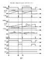
圖3示出根據本公開的各種實施例與圖1中示出的降壓-升壓式轉換器的降壓操作模式相關聯的時序圖。圖3的水平軸表示時間間隔。有12行。第一行401表示由第一鎖存器211生成的PWM信號。第二行402表示饋送到比較器301中的閾值電壓和斜坡信號。第三行403表示比較器301的輸出電壓。第四行404表示由第二鎖存器219生成的PWM信號。第五行405表示饋送到比較器311中的閾值電壓和斜坡信號。第六行406表示比較器311的輸出電壓。第七行407表示饋送到谷值電流比較器214中的檢測的電流信號和誤差放大器電壓。第八行408表示谷值電流比較器214的輸出電壓。第九行409表示開關Q1的栅極驅動信號。第十行410表示開關Q2的栅極驅動信號。第十一行411表示開關Q3的栅極驅動信號。第十二行412表示開關Q4的栅極驅動信號。3 illustrates a timing diagram associated with a buck operating mode of the buck-boost converter shown in FIG. 1 in accordance with various embodiments of the present disclosure. The horizontal axis of FIG. 3 represents time intervals. There are 12 lines. The
在操作中,當降壓-升壓式轉換器的輸入電壓VIN比降壓-升壓式轉換器的輸出電壓VOUT高得多時,升壓轉換器部分的關斷時間比降壓-升壓式轉換器的開關周期長得多。參考圖2,在降壓操作模式中,VRBOOST總是高於k3·(VOUT-VIN)。因此,信號TONBOOST處於邏輯高狀態,這在PWMBOOST處生成邏輯低狀態。響應於PWMBOOST處的邏輯低狀態,高側開關Q4始終打開,並且低側開關Q3始終關閉。降壓轉換器部分的導通時間由降壓導通時間計時器230確定。降壓-升壓式轉換器以降壓操作模式操作。In operation, when the input voltage VIN of the buck-boost converter is much higher than the output voltage VOUT of the buck-boost converter, the turn-off time of the boost converter section is longer than that of the buck-boost converter The switching period of the converter is much longer. Referring to Figure 2, in the buck operating mode, VRBOOST is always higher thank3·(VOUT-VIN) . Therefore, the signal TONBOOST is in a logic high state, which generates a logic low state at the PWMBOOST . In response to a logic low state at PWMBOOST , high-side switch Q4 is always on and low-side switch Q3 is always off. The on-time of the buck converter portion is determined by the buck on-
返回參考圖1,在降壓操作模式中,電流感應放大器213配置成檢測開關Q1的電流(流過電感204的電流)。根據谷值電流模式控制,當電流感應放大器213的輸出達到比較器214的控制電壓VCTRL時,打開開關Q1。在打開開關Q1之後,降壓導通時間計時器230開始計數。一旦降壓導通時間計時器230觸發,便關閉開關Q1,且打開開關Q2。一旦電流感應放大器213的輸出達到比較器214的控制電壓VCTRL,便關閉開關Q2,且再次打開開關Q1,以便開始另一個循環。Referring back to FIG. 1 , in the buck mode of operation, the
圖3示出用於說明降壓操作模式的操作原理的時序圖。在時刻t1,電流感應放大器213的輸出(圖3中的CS)下降並達到比較器214的控制電壓VCTRL。返回參考圖1,在時刻t1,比較器214的輸出生成邏輯電平“1”,並將該邏輯電平“1”發送到第一鎖存器211的設置輸入端。根據R-S鎖存器的操作原理,比較器214的輸出確定開關Q1的栅極驅動信號的導通沿。FIG. 3 shows a timing diagram for explaining the operation principle of the buck operation mode. At time t1 , the output of the current sense amplifier 213 (CS in FIG. 3 ) drops and reaches the control voltage VCTRL of the
如圖3所示,在時刻t1,開關Q2已經關閉,並且開關Q1已經打開。應注意,在打開開關Q1和關閉開關Q2之間有適當的延遲。作為打開開關Q1的結果,從時刻t1到時刻t2,感應電流CS以線性方式增加。從時刻t1到時刻t2,控制信號PWMBUCK具有邏輯高狀態,由此關閉圖2中示出的斜坡信號生成電路的開關305。因此,對斜坡信號電容304充電,並且從時刻t1到時刻t2,電容304兩端的電壓以線性方式增加。在降壓操作模式期間,從不觸發升壓導通時間計時器。通過比較器214的輸出(圖3中的CMP)來復位升壓斜坡信號。As shown in FIG. 3, at time t1, switch Q2 has been closed and switch Q1 has been opened. It should be noted that there is an appropriate delay between opening switch Q1 and closing switch Q2. As a result of opening the switch Q1, the induced current CS increases in a linear manner from the time t1 to the time t2. From time t1 to time t2, the control signal PWMBUCK has a logic high state, thereby turning off the
在時刻t2,斜坡信號電壓VRBUCK達到閾值電壓k1·VOUT。比較器301的輸出生成邏輯電平“1”,並將該邏輯電平“1”發送給第一鎖存器211的復位輸入端。根據R-S鎖存器的操作原理,比較器301的輸出確定開關Q1的栅極驅動信號的關閉沿。At time t2, the ramp signal voltage VRBUCK reaches the threshold voltagek1· VOUT . The output of the
如圖3所示,在時刻t2,通過降壓控制邏輯單元210分別將邏輯電平“1”和邏輯電平“0”施加到Q2和Q1的栅極。作為打開開關Q2並關閉開關Q1的結果,從時刻t2到時刻t3,檢測到的感應電流CS以線性方式減小,並且斜坡信號電容304放電。As shown in FIG. 3, at time t2, a logic level "1" and a logic level "0" are applied to the gates of Q2 and Q1 by the step-down control logic unit 210, respectively. As a result of opening switch Q2 and closing switch Q1, from time t2 to time t3, the sensed current CS detected decreases in a linear manner, and the
在時刻t3,電流感應放大器213的輸出(圖3中的CS)再次達到比較器214的控制電壓VCTRL。降壓-升壓式轉換器進入到新的開關周期。At time t3, the output of the current sense amplifier 213 (CS in FIG. 3 ) reaches the control voltage VCTRL of the
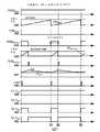
圖4示出根據本公開的各種實施例與圖1中示出的降壓-升壓式轉換器的降壓-升壓操作模式相關聯的時序圖。圖4的水平軸表示時間間隔。有12行。第一行421表示由第一鎖存器211生成的PWM信號。第二行422表示饋送到比較器301中的閾值電壓和斜坡信號。第三行423表示比較器301的輸出電壓。第四行424表示由第二鎖存器219生成的PWM信號。第五行425表示饋送到比較器311中的閾值電壓和斜坡信號。第六行426表示比較器311的輸出電壓。第七行427表示饋送到谷值電流比較器214中的檢測的電流信號和誤差放大器電壓。第八行428表示谷值電流比較器214的輸出電壓。第九行429表示開關Q1的栅極驅動信號。第十行430表示開關Q2的栅極驅動信號。第十一行431表示開關Q3的栅極驅動信號。第十二行432表示開關Q4的栅極驅動信號。4 illustrates a timing diagram associated with a buck-boost mode of operation of the buck-boost converter shown in FIG. 1 in accordance with various embodiments of the present disclosure. The horizontal axis of FIG. 4 represents time intervals. There are 12 lines. The
在操作中,當輸入電壓VIN下降至近似等於輸出電壓VOUT的電平時,即使在輸入電壓VIN仍然高於輸出電壓VOUT時,由於偏移電壓VBIASBOOST,所以升壓轉換器部分的關斷時間減小。當升壓轉換器部分的導通時間(TONBOOST)增加並達到閾值水平時,開關Q4開始關閉,並且開關Q3打開。作為關閉開關Q4和打開開關Q3的結果,降壓-升壓式轉換器以降壓-升壓操作模式操作。In operation, when the input voltage VIN drops to a level approximately equal to the output voltage VOUT, even when the input voltage VIN is still higher than the output voltage VOUT, the off-time of the boost converter section decreases due to the offset voltageVBIASBOOST Small. When the on-time (TONBOOST ) of the boost converter section increases and reaches a threshold level, switch Q4 begins to close and switch Q3 opens. As a result of closing switch Q4 and opening switch Q3, the buck-boost converter operates in a buck-boost mode of operation.
圖4的時序圖示出降壓-升壓操作模式的操作原理。在時刻t1之前,開關Q2和Q4最初處於打開狀態。流過電感的電流(圖4中的CS)以線性方式減小。在時刻t1,感應的電流CS達到控制電壓VCTRL,並且如圖4所示,關閉開關Q2和Q4。在適當的延遲之後,打開開關Q1和Q3。在時刻t1,降壓導通時間計時器230(如圖2所示)和升壓導通時間計時器240(如圖2所示)均開始計數。在一些實施例中,降壓轉換器部分的導通時間(TONBUCK)比升壓轉換器部分的導通時間(TONBOOST)長得多。The timing diagram of FIG. 4 illustrates the principle of operation of the buck-boost mode of operation. Before time t1, switches Q2 and Q4 are initially in an open state. The current through the inductor (CS in Figure 4) decreases linearly. At time t1, the induced current CS reaches the control voltageVCTRL , and as shown in FIG. 4, the switches Q2 and Q4 are closed. After an appropriate delay, switches Q1 and Q3 are opened. At time t1 , both the buck on-time timer 230 (shown in FIG. 2 ) and the boost on-time timer 240 (shown in FIG. 2 ) start counting. In some embodiments, the on-time of the buck converter portion (TONBUCK ) is much longer than the on-time of the boost converter portion (TONBOOST ).
如圖4所示,在時刻t2,觸發升壓導通時間計時器240。作為觸發升壓導通時間計時器240的結果,在時刻t2,關閉開關Q3,並打開開關Q4。在時刻t3,觸發降壓導通時間計時器230。作為觸發降壓導通時間計時器230的結果,在時刻t3,關閉開關Q1,並打開開關Q2。從時刻t3到時刻t4,流過電感的電流(圖4中的CS)以線性方式減小。在時刻t4,感應的電流信號CS達到控制電壓VCTRL,並如圖4所示,關閉開關Q2和Q4。在適當的延遲之後,打開開關Q2和Q3。另一個開關周期開始。As shown in FIG. 4, at time t2, the boost on-
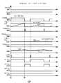
圖5示出根據本公開的各種實施例與圖1中示出的降壓-升壓式轉換器的升壓操作模式相關聯的時序圖。圖5的水平軸表示時間間隔。有12行。第一行441表示由第一鎖存器211生成的PWM信號。第二行442表示饋送到比較器301中的閾值電壓和斜坡信號。第三行443表示比較器301的輸出電壓。第四行444表示由第二鎖存器219生成的PWM信號。第五行445表示饋送到比較器311中的閾值電壓和斜坡信號。第六行446表示比較器311的輸出電壓。第七行447表示饋送到谷值電流比較器214中的檢測的電流信號和誤差放大器電壓。第八行448表示谷值電流比較器214的輸出電壓。第九行449表示開關Q1的栅極驅動信號。第十行450表示開關Q2的栅極驅動信號。第十一行451表示開關Q3的栅極驅動信號。第十二行452表示開關Q4的栅極驅動信號。5 illustrates a timing diagram associated with a boost mode of operation of the buck-boost converter shown in FIG. 1 in accordance with various embodiments of the present disclosure. The horizontal axis of FIG. 5 represents time intervals. There are 12 lines. The
在操作中,輸入電壓VIN下降至低於輸出電壓VOUT的預設電平。該預設電平滿足以下條件:k1·VOUT始終大於VRBUCK。在輸入電壓VIN達到該預設電平之後,如圖5所示,TONBUCK始終是低電平。因此,開關Q1總是打開,並且開關Q2總是關閉。降壓-升壓式轉換器以升壓操作模式操作。In operation, the input voltage VIN drops to a predetermined level lower than the output voltage VOUT. This preset level satisfies the following conditions:k1 ·VOUT is always greater thanVRBUCK . After the input voltage VIN reaches the preset level, as shown in FIG. 5 , TONBUCK is always at a low level. Therefore, switch Q1 is always open and switch Q2 is always closed. The buck-boost converter operates in a boost mode of operation.
圖5的時序圖示出升壓操作模式的操作原理。在升壓操作模式中,降壓導通時間計時器230的輸出始終處於邏輯低狀態。由於降壓導通時間計時器230的輸出始終處於邏輯低狀態,所以開關Q1總是打開,並且開關Q2總是關閉。The timing diagram of FIG. 5 illustrates the principle of operation of the boost mode of operation. In the boost mode of operation, the output of the buck on-
在時刻t1,電流感應放大器213的輸出(圖5中的CS)達到比較器214的控制電壓VCTRL。如上文關於圖2所論述的,在時刻t1,比較器214的輸出(圖5中的CMP)生成邏輯電平“1”,並將該邏輯電平“1”發送到第二鎖存器219的設置輸入端(如圖1所示)。根據R-S鎖存器的操作原理,比較器214的輸出確定開關Q3的栅極驅動信號的導通沿。At time t1 , the output of the current sense amplifier 213 (CS in FIG. 5 ) reaches the control voltage VCTRL of the
如圖5所示,在時刻t1,開關Q4已經關閉。在適當的延遲之後,打開開關Q3。作為打開開關Q3的結果,從時刻t1到時刻t2,感應電流CS以線性方式增加。從時刻t1到時刻t2,控制信號PWMBOOST具有邏輯高狀態。在經過反相器之後,控制信號PWMBOOST關閉圖2中示出的斜坡信號生成電路的開關315。因此,對斜坡信號電容314充電,並且從時刻t1到時刻t2,電容314兩端的電壓以線性方式增加。As shown in FIG. 5, at time t1, switch Q4 has been closed. After an appropriate delay, switch Q3 is opened. As a result of opening the switch Q3, the induced current CS increases in a linear manner from the time t1 to the time t2. From time t1 to time t2, the control signal PWMBOOST has a logic high state. After passing through the inverter, the control signal PWMBOOST turns off the
在時刻t2,斜坡信號電壓VRBOOST達到閾值電壓。比較器311的輸出(TONBOOST)生成邏輯電平“1”,並將該邏輯電平“1”發送到第二鎖存器219的復位輸入端。根據R-S鎖存器的操作原理,比較器311的輸出(TONBOOST)確定開關Q3的栅極驅動信號的關閉沿。At time t2, the ramp signal voltage VRBOOST reaches the threshold voltage. The output of the comparator 311 (TONBOOST ) generates a logic level "1" and sends this logic level "1" to the reset input of the
如圖5所示,通過升壓控制邏輯單元212分別將邏輯電平“0”和邏輯電平“1”施加到開關Q3和Q4的栅極。作為關閉開關Q3並打開開關Q4的結果,從時刻t2到時刻t3,感應電流CS以線性方式減小。在時刻t2,斜坡信號電容314放電。在時刻t3,電流感應放大器213的輸出(圖3中的CS)再次達到比較器214的控制電壓VCTRL。降壓-升壓式轉換器進入到新的開關周期。As shown in FIG. 5, a logic level "0" and a logic level "1" are applied to the gates of switches Q3 and Q4, respectively, by the boost
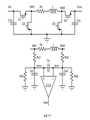
圖6示出根據本公開的各種實施例的另一個降壓-升壓式轉換器及其相關聯的恆定導通時間控制電路的示意圖。圖6中示出的降壓-升壓式轉換器與圖1中示出的降壓-升壓式轉換器類似,不同之處在於,通過控制單元550來確定操作模式轉變。特別地,控制單元550根據輸入電壓VIN和輸出電壓VOUT之間的關係來確定降壓-升壓式轉換器以哪種操作模式(降壓、降壓-升壓或升壓)操作。6 shows a schematic diagram of another buck-boost converter and its associated constant on-time control circuit according to various embodiments of the present disclosure. The buck-boost converter shown in FIG. 6 is similar to the buck-boost converter shown in FIG. 1 , except that the operating mode transition is determined by the
如圖6所示,控制單元550包括第一比較器551和第二比較器553。第一比較器551具有連接到輸出電壓VOUT和第一偏移電壓VOFFSET1的總和的同相輸入端。第一比較器551具有連接到輸入電壓VIN的反相輸入端。基於輸入電壓VIN和輸出電壓VOUT之間的關係將第一比較器551的輸出施加到降壓-升壓式轉換器的升壓轉換器部分的控制電路。As shown in FIG. 6 , the
第二比較器553具有連接到輸入電壓VIN的同相輸入端。第一比較器551具有連接到等於輸出電壓VOUT減去第二偏移電壓VOFFSET2的電壓電平的反相輸入端。基於輸入電壓VIN和輸出電壓VOUT之間的關係將第二比較器553的輸出施加到降壓-升壓式轉換器的降壓轉換器部分的控制電路。The
應注意,第一偏移電壓VOFFSET1和第二偏移電壓VOFFSET2均是預先設定的。基於不同應用和設計需要,第一偏移電壓VOFFSET1和第二偏移電壓VOFFSET2的值可相應地改變。It should be noted that both the first offset voltage VOFFSET1 and the second offset voltage VOFFSET2 are preset. Based on different applications and design requirements, the values of the first offset voltage VOFFSET1 and the second offset voltage VOFFSET2 may be changed accordingly.
圖7示出根據本公開的各種實施例在圖6中示出的降壓導通時間計時器和升壓導通時間計時器的示意圖。降壓導通時間計時器530和升壓導通時間計時器540與圖2中示出的計時器類似,不同之處在於,利用圖6中示出的比較器551和553的輸出來確定降壓-升壓式轉換器的操作模式。7 illustrates a schematic diagram of the buck on-time timer and the boost on-time timer shown in FIG. 6 in accordance with various embodiments of the present disclosure. Buck on-
如圖7所示,“與”門601配置成接收由第二比較器553生成的BKM信號。採用BKM信號來啓用降壓-升壓式轉換器的降壓轉換器部分。BKM信號還用於復位斜坡信號電容605。如圖7所示,將PWMBUCK信號和BKM信號饋送到“與非”門607中。利用“與非”門607的輸出來復位斜坡信號電容605。As shown in FIG. 7 , the AND
如圖7所示,“或”門611配置成接收由第一比較器551生成的BSTM信號。採用BSTM信號來啓用降壓-升壓式轉換器的升壓轉換器部分。BSTM信號還用於復位斜坡信號電容617。如圖7所示,將PWMBOOST信號和BSTM信號饋送到“與非”門616中。利用“與非”門616的輸出來復位斜坡信號電容617。As shown in FIG. 7 , the
圖8示出根據本公開的各種實施例在圖6中示出的比較器的操作原理。在圖8中,當輸入電壓VIN高於VOUT + VOFFSET1時,降壓-升壓式轉換器禁用升壓操作模式,並以降壓操作模式操作。返回參考圖6,控制電路生成PWM信號(例如,PWMBUCK),並將PWM信號施加到開關Q1和Q2。在該操作模式中,開關Q3總是關閉,並且開關Q4總是打開。FIG. 8 illustrates the principle of operation of the comparator shown in FIG. 6 according to various embodiments of the present disclosure. In Figure 8, when the input voltage VIN is higher than VOUT + VOFFSET1, the buck-boost converter disables the boost mode of operation and operates in the buck mode of operation. Referring back to FIG. 6, the control circuit generates a PWM signal (eg, PWMBUCK ) and applies the PWM signal to switches Q1 and Q2. In this mode of operation, switch Q3 is always closed and switch Q4 is always open.
在操作中,當輸入電壓VIN低於VOUT – VOFFSET2時,降壓-升壓式轉換器禁用降壓操作模式,並以升壓操作模式操作。返回參考圖6,控制電路生成PWM信號(例如,PWMBOOST),並將PWM信號施加到開關Q3和Q4。在該操作模式中,開關Q2總是關閉,並且開關Q1總是打開。In operation, when the input voltage VIN is lower than VOUT – VOFFSET2, the buck-boost converter disables the buck mode of operation and operates in the boost mode of operation. Referring back to FIG. 6, the control circuit generates a PWM signal (eg, PWMBOOST ) and applies the PWM signal to switches Q3 and Q4. In this mode of operation, switch Q2 is always closed and switch Q1 is always open.
操作中,當輸入電壓VIN介於VOUT – VOFFSET2和VOUT + VOFFSET1之間時,降壓-升壓式轉換器以降壓-升壓操作模式操作。在每個開關循環期間,控制電路可開關所有四個開關。In operation, the buck-boost converter operates in a buck-boost mode of operation when the input voltage VIN is between VOUT – VOFFSET2 and VOUT + VOFFSET1. During each switching cycle, the control circuit can switch all four switches.
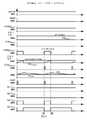
圖9示出根據本公開的各種實施例與圖6中示出的降壓-升壓式轉換器的降壓操作模式相關聯的時序圖。圖9的水平軸表示時間間隔。有14行。第一行801表示由比較器551生成的BSTM信號。第二行802表示由比較器553生成的BKM信號。第三行803表示由第一鎖存器512生成的PWM信號。第四行804表示饋送到比較器602中的閾值電壓和斜坡信號。第五行805表示“與”門601的輸出電壓。第六行806表示由第二鎖存器519生成的PWM信號。第七行807表示饋送到比較器612中的閾值電壓和斜坡信號。第八行808表示“或”門611的輸出電壓。第九行809表示饋送到谷值電流比較器514中的檢測的電流信號和誤差放大器電壓。第十行810表示谷值電流比較器514的輸出電壓。第十一行811表示開關Q1的栅極驅動信號。第十二行812表示開關Q2的栅極驅動信號。第十三行813表示開關Q3的栅極驅動信號。第十四行814表示開關Q4的栅極驅動信號。9 illustrates a timing diagram associated with a buck operating mode of the buck-boost converter shown in FIG. 6 in accordance with various embodiments of the present disclosure. The horizontal axis of FIG. 9 represents time intervals. There are 14 lines. The
圖9中示出的時序圖與圖3中示出的時序圖類似,不同之處在於,採用BSTM信號和BKM信號來確定降壓-升壓式轉換器的操作模式。在降壓操作模式中,BSTM信號具有邏輯低狀態,如圖9所示。BKM信號具有邏輯高狀態,如圖9所示。利用BSTM信號的邏輯低狀態來禁用升壓操作模式。如圖9所示,PWMBOOST信號具有邏輯低狀態。此類邏輯低狀態使開關Q3保持始終關閉,並使Q4保持始終打開。通過反相器603將BKM信號的邏輯高狀態饋送到“或”門601中。反相的BKM信號是邏輯低信號,其對降壓轉換器部分的操作沒有影響。The timing diagram shown in Figure 9 is similar to the timing diagram shown in Figure 3, except that the BSTM signal and the BKM signal are used to determine the operating mode of the buck-boost converter. In the buck mode of operation, the BSTM signal has a logic low state, as shown in Figure 9. The BKM signal has a logic high state, as shown in Figure 9. The boost mode of operation is disabled with a logic low state of the BSTM signal. As shown in Figure 9, the PWMBOOST signal has a logic low state. Such a logic low state keeps switch Q3 always off and Q4 always on. The logic high state of the BKM signal is fed into OR
圖10示出根據本公開的各種實施例與圖6中示出的降壓-升壓式轉換器的降壓-升壓操作模式相關聯的時序圖。圖10的水平軸表示時間間隔。有14行。第一行821表示由比較器551生成的BSTM信號。第二行822表示由比較器553生成的BKM信號。第三行823表示由第一鎖存器512生成的PWM信號。第四行824表示饋送到比較器602中的閾值電壓和斜坡信號。第五行825表示“與”門601的輸出電壓。第六行826表示由第二鎖存器519生成的PWM信號。第七行827表示饋送到比較器612中的閾值電壓和斜坡信號。第八行828表示“或”門611的輸出電壓。第九行829表示饋送到谷值電流比較器514中的檢測的電流信號和誤差放大器電壓。第十行830表示谷值電流比較器514的輸出電壓。第十一行831表示開關Q1的栅極驅動信號。第十二行832表示開關Q2的栅極驅動信號。第十三行833表示開關Q3的栅極驅動信號。第十四行834表示開關Q4的栅極驅動信號。10 shows a timing diagram associated with the buck-boost mode of operation of the buck-boost converter shown in FIG. 6 in accordance with various embodiments of the present disclosure. The horizontal axis of FIG. 10 represents time intervals. There are 14 lines. The
圖10中示出的時序圖與圖4中示出的時序圖類似,不同之處在於,採用BSTM信號和BKM信號來確定降壓-升壓式轉換器的操作模式。在降壓-升壓操作模式中,BSTM信號和BKM信號均處於邏輯高狀態,如圖10所示。利用BSTM信號的邏輯高狀態來啓用升壓轉換器部分。如圖10所示,在每個開關循環中,打開和關閉開關Q3和Q4。利用BKM信號的邏輯高狀態來啓用降壓轉換器部分。如圖10所示,在每個開關循環中,打開和關閉開關Q1和Q2。The timing diagram shown in Figure 10 is similar to the timing diagram shown in Figure 4, except that the BSTM signal and the BKM signal are used to determine the operating mode of the buck-boost converter. In the buck-boost mode of operation, both the BSTM signal and the BKM signal are in a logic high state, as shown in Figure 10. The boost converter section is enabled with a logic high state of the BSTM signal. As shown in Figure 10, in each switching cycle, switches Q3 and Q4 are opened and closed. The buck converter section is enabled with a logic high state of the BKM signal. As shown in Figure 10, in each switching cycle, switches Q1 and Q2 are opened and closed.
圖11示出根據本公開的各種實施例與圖6中示出的降壓-升壓式轉換器的升壓操作模式相關聯的時序圖。圖11的水平軸表示時間間隔。有14行。第一行841表示由比較器551生成的BSTM信號。第二行842表示由比較器553生成的BKM信號。第三行843表示由第一鎖存器512生成的PWM信號。第四行844表示饋送到比較器602中的閾值電壓和斜坡信號。第五行845表示“與”門601的輸出電壓。第六行846表示由第二鎖存器519生成的PWM信號。第七行847表示饋送到比較器612中的閾值電壓和斜坡信號。第八行848表示“或”門611的輸出電壓。第九行849表示饋送到谷值電流比較器514中的檢測的電流信號和誤差放大器電壓。第十行850表示谷值電流比較器514的輸出電壓。第十一行851表示開關Q1的栅極驅動信號。第十二行852表示開關Q2的栅極驅動信號。第十三行853表示開關Q3的栅極驅動信號。第十四行854表示開關Q4的栅極驅動信號。11 shows a timing diagram associated with the boost mode of operation of the buck-boost converter shown in FIG. 6 in accordance with various embodiments of the present disclosure. The horizontal axis of FIG. 11 represents time intervals. There are 14 lines. The first row 841 represents the BSTM signal generated by the
圖11中示出的時序圖與圖5中示出的時序圖類似,不同之處在於,採用BSTM信號和BKM信號來確定降壓-升壓式轉換器的操作模式。在升壓操作模式中,BSTM信號具有邏輯高狀態,如圖11所示。BKM信號具有邏輯低狀態,如圖11所示。利用BKM信號的邏輯低狀態來禁用降壓操作模式。如圖11所示,PWMBUCK信號具有邏輯高狀態。此類邏輯高狀態使開關Q2保持始終關閉並使開關Q1保持始終打開。將BSTM信號的邏輯高狀態饋送到“或”門611中。BSTM的邏輯高信號對升壓轉換器部分的操作沒有影響。The timing diagram shown in Figure 11 is similar to the timing diagram shown in Figure 5, except that the BSTM signal and the BKM signal are used to determine the operating mode of the buck-boost converter. In the boost mode of operation, the BSTM signal has a logic high state, as shown in Figure 11. The BKM signal has a logic low state, as shown in Figure 11. The buck mode of operation is disabled with a logic low state of the BKM signal. As shown in Figure 11, the PWMBUCK signal has a logic high state. Such logic high states keep switch Q2 always closed and switch Q1 always open. The logic high state of the BSTM signal is fed into OR
圖12示出根據本公開的各種實施例用於檢測流過降壓-升壓式轉換器的電感的電流的電流感應電路的第一實現的示意圖。返回參考圖1和圖6,可採用諸如直流電阻(DCR)電流感應裝置的電流感應裝置來檢測流過降壓-升壓式轉換器的電感的電流。圖12示出DCR電流感應裝置的第一實現的示意圖。如圖12所示,電感連接在開關節點SW1和SW2之間。RL表示電感的等效串聯電阻。如圖12所示,RL與電感L串聯連接。12 shows a schematic diagram of a first implementation of a current sensing circuit for detecting current flowing through an inductor of a buck-boost converter in accordance with various embodiments of the present disclosure. Referring back to Figures 1 and 6, a current sensing device, such as a direct current resistance (DCR) current sensing device, may be employed to sense the current flowing through the inductor of the buck-boost converter. Figure 12 shows a schematic diagram of a first implementation of a DCR current sensing device. As shown in FIG. 12, the inductor is connected between switching nodes SW1 and SW2. RL represents the equivalent series resistance of the inductor. As shown in Figure 12, RL is connected in series with the inductor L.
如圖12所示,DCR電流感應裝置包括Rs1、Rs2、Cs1和Cs2。Rs1和Cs1串聯連接在開關節點SW1和地之間。Rs2和Cs2串聯連接在開關節點SW2和地之間。Rs1和Cs1的公共節點連接到電流感應放大器213的同相輸入端。Rs2和Cs2的公共節點連接到電流感應放大器213的反相輸入端。在一些實施例中,DCR感應裝置與控制電路以及功率裝置集成在一起。As shown in FIG. 12, the DCR current sensing device includes Rs1, Rs2, Cs1 and Cs2. Rs1 and Cs1 are connected in series between switch node SW1 and ground. Rs2 and Cs2 are connected in series between switch node SW2 and ground. The common node of Rs1 and Cs1 is connected to the non-inverting input of the
SW1和SW2是開關節點。Rs1、Rs2、Cs1和Cs2形成兩個濾波器,這兩個濾波器可過濾掉SW1和SW2處的脉動電壓,並將脉動電壓轉換為饋送到電流感應放大器213中的合適的直流電壓。為了更好地衰減脉動電壓,通過以下等式給定兩個濾波器的分量值:
在以上等式中,L是降壓-升壓式轉換器的電感。RL是電感的等效串聯電阻。Rs是感應電阻(Rs1和Rs2)的電阻值。Cs是感應電容(Cs1和Cs2)的電容值。在一些實施例中,Isns+和Isns-之間的電壓與流過電感L的電流成比例。In the above equation, L is the inductance of the buck-boost converter. RL is the equivalent series resistance of the inductor. Rs is the resistance value of the sense resistors (Rs1 and Rs2). Cs is the capacitance value of the sense capacitors (Cs1 and Cs2). In some embodiments, the voltage between Isns+ and Isns- is proportional to the current flowing through the inductor L.
圖13示出根據本公開的各種實施例用於檢測流過降壓-升壓式轉換器的電感的電流的電流感應電路的第二實現的示意圖。圖13中示出的電流感應電路與圖12中示出的電流感應電路類似,不同之處在於,在電流感應放大器213的兩個輸入端之間放置電容Cs0。在該實現中,通過以下等式給定兩個濾波器的分量值:
具有Cs0的一個有利特徵是,該電容有助於減少由Cs1和Cs2之間的不匹配造成的感應誤差。如圖13所示,電容Cs1和Cs2分別連接到SW1和SW2。那兩個電容之間的不匹配可對感應的電壓(電流感應放大器213的兩個輸入端之間的電壓)造成顯著誤差。由於感應的輸出在幾十mV範圍內,所以電流感應電路的性能極度依賴於兩個電容(Cs1和Cs2)之間的匹配。另一個問題與電容的電壓係數有關。響應於不同的輸入和輸出電壓,電容上的直流電壓可在廣泛範圍內改變。利用不同的直流偏置電壓,陶瓷電容(例如,Cs1和Cs2)的實際電容可顯著改變。An advantageous feature of having Cs0 is that the capacitance helps reduce inductive errors caused by the mismatch between Cs1 and Cs2. As shown in FIG. 13, capacitors Cs1 and Cs2 are connected to SW1 and SW2, respectively. The mismatch between those two capacitors can cause significant errors to the induced voltage (the voltage between the two inputs of the current sense amplifier 213). Since the sensed output is in the range of tens of mV, the performance of the current sensing circuit is extremely dependent on the matching between the two capacitors (Cs1 and Cs2). Another problem has to do with the voltage coefficient of the capacitor. The DC voltage across the capacitor can vary over a wide range in response to different input and output voltages. The actual capacitance of ceramic capacitors (eg, Cs1 and Cs2) can vary significantly with different DC bias voltages.
在如圖13所示的實現中,Cs0/Cs1或Cs0/Cs2的比例遠大於1。換句話說,A遠大於1。A是預設值。通過選擇合適的A,Cs1和Cs2的電壓係數的不匹配可對感應性能具有輕微的影響。同時,Cs(Cs1和Cs2)上的電壓變化接近於0。因此,DCR感應電路不具有電壓係數問題。In the implementation shown in Figure 13, the ratio of Cs0/Cs1 or Cs0/Cs2 is much greater than one. In other words, A is much larger than 1. A is the default value. By choosing a suitable A, the mismatch in the voltage coefficients of Cs1 and Cs2 can have a slight impact on the sensing performance. At the same time, the voltage variation on Cs (Cs1 and Cs2) is close to zero. Therefore, DCR sensing circuits do not have voltage coefficient problems.
圖14示出根據本公開的各種實施例用於檢測流過降壓-升壓式轉換器的電感的電流的電流感應電路的第三實現的示意圖。圖14中示出的電流感應電路與圖13中示出的電流感應電路類似,不同之處在於,通過去除Cs1和Cs2來進一步簡化電流感應電路。在該實現中,通過以下等式給定兩個濾波器的分量值:
在以上等式中,Rs是Rs1和Rs2的電阻值。In the above equation, Rs is the resistance value of Rs1 and Rs2.
圖15示出根據本公開的各種實施例用於檢測流過降壓-升壓式轉換器的電感的電流的電流感應電路的第四實現的示意圖。圖15中示出的電流感應電路與圖13中示出的電流感應電路類似,不同之處在於,在電流感應電路中增加兩個額外的電阻Rd1和Rd2。利用這兩個電阻,Isns+和Isns-上的電壓總是低於輸入電壓或輸出電壓。該電路可簡化電流感應放大器的設計。通過以下等式給定電流感應電路的分量值:
圖16示出根據本公開的各種實施例用於檢測流過降壓-升壓式轉換器的電感的電流的電流感應電路的第五實現的示意圖。圖16中示出的電流感應電路與圖15中示出的電流感應電路類似,不同之處在於,通過去除Cs1和Cs2簡化了電流感應電路。通過以下等式確定Cs0:
儘管詳細描述了本發明的實施例和其優點,但是應瞭解,在不偏離由隨附請求項定義的本發明的精神和範圍的情况下,可在本文中進行各種改變、替換和變更。Although the embodiments of the present invention and their advantages have been described in detail, it should be understood that various changes, substitutions and alterations can be made herein without departing from the spirit and scope of the invention as defined by the appended claims.
此外,不希望將本申請的範圍局限於本說明書中描述的過程、機器、製造、物質組成、方式、方法和步驟的特定實施例。本領域技術人員將從本發明的公開容易地明白,根據本發明,可利用目前現有或稍後開發的用於與本文中描述的對應實施例執行大體上相同的功能或實現大體上相同的結果的過程、機器、製造、物質組成、方式、方法或步驟。因此,希望隨附請求項在它們的範圍內包含此類過程、機器、製造、物質組成、方式、方法或步驟。Furthermore, there is no intention to limit the scope of this application to the particular embodiments of the process, machine, manufacture, composition of matter, means, methods and steps described in this specification. Those skilled in the art will readily appreciate from the disclosure of the present invention that, in accordance with the present invention, currently existing or later developed corresponding embodiments may be utilized to perform substantially the same functions or achieve substantially the same results as those described herein. process, machine, manufacture, composition of matter, manner, method or step. Accordingly, the appended claims are intended to include within their scope such processes, machines, manufacture, compositions of matter, means, methods, or steps.
Q1:開關Q2:開關Q3:開關Q4:開關201:輸入電容204:電感207:輸出電容208:電阻209:電阻210:降壓控制邏輯單元211:第一鎖存器212:升壓控制邏輯單元213:電流感應放大器214:比較器215:電阻216:電容217:電容218:放大器219:第二鎖存器230:降壓導通時間計時器240:升壓導通時間計時器301:比較器302:降壓偏置電壓源303:電流源304:電容305:開關306:門307:反相器311:比較器312:升壓偏置電壓源313:電流源314:電容315:開關316:門317:反相器401:第一行402:第二行403:第三行404:第四行405:第五行406:第六行407:第七行408:第八行409:第九行410:第十行411:第十一行412:第十二行421:第一行422:第二行421:第一行424:第四行425:第五行423:第三行426:第六行427:第七行428:第八行429:第九行430:第十行431:第十一行432:第十二行441:第一行442:第二行443:第三行444:第四行445:第五行446:第六行447:第七行448:第八行449:第九行450:第十行451:第十一行452:第十二行512:第一鎖存器514:比較器530:降壓導通時間計時器540:升壓導通時間計時器550:控制單元551:比較器553:比較器601:門602:比較器603:反相器605:斜坡信號電容607:門611:門612:比較器616:門617:電容801:第一行802:第二行803:第三行804:第四行805:第五行806:第六行807:第七行808:第八行809:第九行810:第十行811:第十一行812:第十二行813:第十三行814:第十四行821:第一行822:第二行823:第三行824:第四行825:第五行826:第六行827:第七行828:第八行829:第九行830:第十行831:第十一行832:第十二行833:第十三行834:第十四行841:第一行842:第二行843:第三行844:第四行845:第五行846:第六行847:第七行848:第八行849:第九行850:第十行851:第十一行852:第十二行853:第十三行854:第十四行VOUT:輸出電壓VREF:參考電壓VIN:輸入電壓Rd1,Rd2:電阻t1,t2,t3,t4:時刻CS:電流VOFFSET1:第一偏移電壓VOFFSET2:第二偏移電壓Q1: switchQ2: switchQ3: switchQ4: Switch201: Input Capacitance204: Inductance207: output capacitor208: Resistor209: Resistor210: Buck Control Logic Unit211: first latch212: boost control logic unit213: Current Sense Amplifier214: Comparator215: Resistor216: Capacitor217: Capacitor218: Amplifier219: second latch230: Buck On-Time Timer240: Boost on-time timer301: Comparator302: Buck Bias Voltage Source303: Current Source304: Capacitor305: switch306: Door307: Inverter311: Comparator312: Boost Bias Voltage Source313: Current source314: Capacitor315: switch316: Door317: Inverter401: first line402: second line403: third line404: Fourth line405: Fifth line406: Sixth line407: Seventh line408: Line Eight409: ninth line410: Line Ten411: Line 11412: line 12421: first line422: second line421: first line424: fourth line425: Fifth line423: third line426: Sixth line427: Seventh line428: eighth line429: ninth line430: tenth line431: Line 11432: line 12441: first line442: second line443: third line444: Fourth line445: Fifth line446: Sixth line447: Seventh line448: Line Eight449: ninth line450: tenth line451: Line 11452: line 12512: first latch514: Comparator530: Buck On-Time Timer540: Boost on-time timer550: Control Unit551: Comparator553: Comparator601: Door602: Comparator603: Inverter605: Ramp signal capacitor607: Door611: Door612: Comparator616: Door617: Capacitor801: first line802: second line803: Third line804: Fourth line805: Fifth line806: Sixth line807: Seventh line808: Line Eight809: ninth line810: Line Ten811: Line 11812: line 12813: line thirteen814: line fourteen821: first line822: second line823: third line824: Fourth line825: Fifth line826: Sixth line827: Seventh line828: eighth line829: ninth line830: Line Ten831: Line 11832: line 12833: line thirteen834: line fourteen841: first line842: second line843: third line844: Fourth line845: Fifth line846: Sixth line847: Seventh line848: Line 8849: ninth line850: tenth line851: Line 11852: line 12853: line thirteen854: line fourteenVOUT: output voltageVREF: reference voltageVIN: input voltageRd1, Rd2: resistancet1,t2,t3,t4: momentsCS: CurrentVOFFSET1: The first offset voltageVOFFSET2: Second offset voltage
[圖1] 示出根據本公開的各種實施例的降壓-升壓式轉換器及其相關聯的恆定導通時間控制電路的示意圖。[圖2] 示出根據本公開的各種實施例的降壓導通時間計時器和升壓導通時間計時器的示意圖。[圖3] 示出根據本公開的各種實施例與圖1中示出的降壓-升壓式轉換器的降壓操作模式相關聯的時序圖。[圖4] 示出根據本公開的各種實施例與圖1中示出的降壓-升壓式轉換器的降壓-升壓操作模式相關聯的時序圖。[圖5] 示出根據本公開的各種實施例與圖1中示出的降壓-升壓式轉換器的升壓操作模式相關聯的時序圖。[圖6] 示出根據本公開的各種實施例的另一個降壓-升壓式轉換器及其相關聯的恆定導通時間控制電路的示意圖。[圖7] 示出根據本公開的各種實施例在圖6中示出的降壓導通時間計時器和升壓導通時間計時器的示意圖。[圖8] 示出根據本公開的各種實施例在圖6中示出的比較器的操作原理。[圖9] 示出根據本公開的各種實施例與圖6中示出的降壓-升壓式轉換器的降壓操作模式相關聯的時序圖。[圖10] 示出根據本公開的各種實施例與圖6中示出的降壓-升壓式轉換器的降壓-升壓操作模式相關聯的時序圖。[圖11] 示出根據本公開的各種實施例與圖6中示出的降壓-升壓式轉換器的升壓操作模式相關聯的時序圖。[圖12] 示出根據本公開的各種實施例用於檢測流過降壓-升壓式轉換器的電感的電流的電流感應電路的第一實現的示意圖。[圖13] 示出根據本公開的各種實施例用於檢測流過降壓-升壓式轉換器的電感的電流的電流感應電路的第二實現的示意圖。[圖14] 示出根據本公開的各種實施例用於檢測流過降壓-升壓式轉換器的電感的電流的電流感應電路的第三實現的示意圖。[圖15] 示出根據本公開的各種實施例用於檢測流過降壓-升壓式轉換器的電感的電流的電流感應電路的第四實現的示意圖。[圖16] 示出根據本公開的各種實施例用於檢測流過降壓-升壓式轉換器的電感的電流的電流感應電路的第五實現的示意圖。[ FIG. 1 ] A schematic diagram illustrating a buck-boost converter and its associated constant on-time control circuit according to various embodiments of the present disclosure.[ FIG. 2 ] A schematic diagram illustrating a buck on-time timer and a boost on-time timer according to various embodiments of the present disclosure.[ FIG. 3 ] shows a timing diagram associated with a buck operation mode of the buck-boost converter shown in FIG. 1 according to various embodiments of the present disclosure.[ FIG. 4 ] shows a timing diagram associated with a buck-boost operation mode of the buck-boost converter shown in FIG. 1 according to various embodiments of the present disclosure.[ FIG. 5 ] shows a timing diagram associated with a boost operation mode of the buck-boost converter shown in FIG. 1 according to various embodiments of the present disclosure.[ FIG. 6 ] A schematic diagram showing another buck-boost converter and its associated constant on-time control circuit according to various embodiments of the present disclosure.[ FIG. 7 ] A schematic diagram illustrating the buck on-time timer and the boost on-time timer shown in FIG. 6 according to various embodiments of the present disclosure.[ FIG. 8 ] illustrates an operation principle of the comparator shown in FIG. 6 according to various embodiments of the present disclosure.[ FIG. 9 ] shows a timing diagram associated with the buck operation mode of the buck-boost converter shown in FIG. 6 according to various embodiments of the present disclosure.[ FIG. 10 ] shows a timing diagram associated with the buck-boost operation mode of the buck-boost converter shown in FIG. 6 according to various embodiments of the present disclosure.[ FIG. 11 ] shows a timing diagram associated with the boost operation mode of the buck-boost converter shown in FIG. 6 according to various embodiments of the present disclosure.[ FIG. 12 ] A schematic diagram showing a first implementation of a current sensing circuit for detecting current flowing through an inductor of a buck-boost converter according to various embodiments of the present disclosure.[ FIG. 13 ] A schematic diagram illustrating a second implementation of a current sensing circuit for detecting current flowing through an inductor of a buck-boost converter according to various embodiments of the present disclosure.[ FIG. 14 ] A schematic diagram showing a third implementation of a current sensing circuit for detecting current flowing through an inductor of a buck-boost converter according to various embodiments of the present disclosure.[ FIG. 15 ] A schematic diagram showing a fourth implementation of a current sensing circuit for detecting current flowing through an inductor of a buck-boost converter according to various embodiments of the present disclosure.[ FIG. 16 ] A schematic diagram showing a fifth implementation of a current sensing circuit for detecting current flowing through an inductor of a buck-boost converter according to various embodiments of the present disclosure.
Q1:第一高側開關Q1: The first high-side switch
Q2:第一低側開關Q2: The first low-side switch
Q3:第二低側開關Q3: Second low side switch
Q4:第二高側開關Q4: Second high side switch
204:電感204: Inductance
207:輸出電容207: output capacitor
208:電阻208: Resistor
209:電阻209: Resistor
210:降壓控制邏輯單元210: Buck Control Logic Unit
211:第一鎖存器211: first latch
212:升壓控制邏輯單元212: boost control logic unit
213:電流感應放大器213: Current Sense Amplifier
214:比較器214: Comparator
215:電阻215: Resistor
216:電容216: Capacitor
217:電容217: Capacitor
218:放大器218: Amplifier
219:第二鎖存器219: second latch
230:降壓導通時間計時器230: Buck On-Time Timer
240:升壓導通時間計時器240: Boost on-time timer
VOUT:輸出電壓VOUT: output voltage
VREF:參考電壓VREF: reference voltage
VIN:輸入電壓VIN: input voltage
Claims (20)
Translated fromChineseApplications Claiming Priority (2)
| Application Number | Priority Date | Filing Date | Title |
|---|---|---|---|
| US16/716,681 | 2019-12-17 | ||
| US16/716,681US10992231B1 (en) | 2019-12-17 | 2019-12-17 | Buck-boost converter and control method |
Publications (2)
| Publication Number | Publication Date |
|---|---|
| TW202127170A TW202127170A (en) | 2021-07-16 |
| TWI764447Btrue TWI764447B (en) | 2022-05-11 |
Family
ID=75587387
Family Applications (1)
| Application Number | Title | Priority Date | Filing Date |
|---|---|---|---|
| TW109144807ATWI764447B (en) | 2019-12-17 | 2020-12-17 | Buck-boost converter and control method |
Country Status (3)
| Country | Link |
|---|---|
| US (2) | US10992231B1 (en) |
| CN (1) | CN112994455B (en) |
| TW (1) | TWI764447B (en) |
Families Citing this family (16)
| Publication number | Priority date | Publication date | Assignee | Title |
|---|---|---|---|---|
| CN114981747B (en) | 2020-01-02 | 2024-02-09 | 德州仪器公司 | Current mode DC-DC converter |
| US11323029B2 (en)* | 2020-04-24 | 2022-05-03 | Silicon Laboratories Inc. | System and method of automatic calibration to maximize load current support of DC-DC converter operating in pulse-pairing mode |
| CN112019048B (en)* | 2020-08-20 | 2022-03-22 | 成都芯源系统有限公司 | Switching converter, controller and control method thereof |
| US11671013B2 (en)* | 2020-09-02 | 2023-06-06 | Cypress Semiconductor Corporation | Control logic performance optimizations for universal serial bus power delivery controller |
| US11821927B2 (en)* | 2020-09-02 | 2023-11-21 | Cypress Semiconductor Corporation | High-voltage tolerant, high-speed reverse current detection and protection for buck-boost converters |
| US11705811B2 (en) | 2020-11-10 | 2023-07-18 | M3 Technology Inc. | Buck-boost converter and hybrid control method |
| US11552555B2 (en)* | 2020-12-31 | 2023-01-10 | Texas Instruments Incorporated | Circuit electromagnetic interference control |
| CN113410989B (en)* | 2021-07-13 | 2022-10-04 | 上海艾为电子技术股份有限公司 | Digital booster circuit, control method thereof and electronic equipment |
| CN113497560B (en)* | 2021-07-23 | 2022-07-19 | 广州金升阳科技有限公司 | Control method of buck-boost converter |
| CN113422513B (en)* | 2021-08-04 | 2023-01-24 | 上海南芯半导体科技股份有限公司 | Control method of BUCK-BOOST converter |
| CN113437873B (en)* | 2021-08-04 | 2023-02-07 | 上海南芯半导体科技股份有限公司 | Self-adaptive control method of BUCK-BOOST converter |
| CN114448249B (en)* | 2021-12-30 | 2024-11-15 | 河海大学 | Fully digital soft-switching control circuit for four-switch buck-boost bidirectional converter |
| US12074529B2 (en)* | 2022-05-05 | 2024-08-27 | Cypress Semiconductor Corporation | Voltage bus discharge for universal serial bus power delivery |
| CN114825935B (en)* | 2022-05-25 | 2025-07-11 | 中国电子科技集团公司第四十三研究所 | A dual-time-scale optimal control method for a four-switch buck-boost converter |
| CN115498861B (en)* | 2022-09-22 | 2024-10-15 | 上海南芯半导体科技股份有限公司 | Power supply control circuit based on peak-valley value current mode |
| US20240136928A1 (en)* | 2022-10-13 | 2024-04-25 | Renesas Design (UK) Limited | Control circuit for a buck-boost power converter |
Citations (13)
| Publication number | Priority date | Publication date | Assignee | Title |
|---|---|---|---|---|
| WO1999041826A1 (en)* | 1998-02-11 | 1999-08-19 | Powerdsine Ltd. | Pwm controller for use with open loop dc to ac converter |
| US20090251122A1 (en)* | 2005-12-29 | 2009-10-08 | Pramod Singnurkar | Method for DC/DC Conversion and DC/DC Converter Arrangement |
| TW201108580A (en)* | 2009-07-22 | 2011-03-01 | Wolfson Microelectronics Plc | Improvements relating to DC-DC converters |
| US20110199062A1 (en)* | 2007-08-20 | 2011-08-18 | Austriamicrosystems Ag | DC/DC Converter Arrangement and Method for DC/DC Conversion |
| US20120105030A1 (en)* | 2010-10-28 | 2012-05-03 | Richtek Technology Corp. | Control circuit and method for a current mode controlled power converter |
| CN102570808A (en)* | 2010-12-27 | 2012-07-11 | 三美电机株式会社 | Switching-mode power supply device |
| WO2014043219A2 (en)* | 2012-09-11 | 2014-03-20 | Analog Devices, Inc. | Dc to dc converter, controller, and control techniques |
| US20140217996A1 (en)* | 2013-02-06 | 2014-08-07 | Microsemi Corporation | Hysteretic current mode control converter with low, medium and high current thresholds |
| EP2683068B1 (en)* | 2012-07-06 | 2014-09-10 | Nxp B.V. | Control circuit for a switched-mode power supply |
| CN104205593A (en)* | 2012-03-29 | 2014-12-10 | 株式会社自动网络技术研究所 | Power source device |
| TW201501119A (en)* | 2013-06-18 | 2015-01-01 | Intersil Americas LLC | Audio frequency deadband system and method for switch mode regulators operating in discontinuous conduction mode |
| CN109314459A (en)* | 2016-04-15 | 2019-02-05 | 艾默生环境优化技术有限公司 | Circuit of power factor correction and include for the Partial Power factor correcting of boost power converter and buck power converter operation method |
| CN110323944A (en)* | 2018-03-28 | 2019-10-11 | 来颉科技股份有限公司 | The constant-off-time of improved four switch buck-boosts formula converter controls |
Family Cites Families (3)
| Publication number | Priority date | Publication date | Assignee | Title |
|---|---|---|---|---|
| US8773084B2 (en)* | 2009-08-24 | 2014-07-08 | Micrel, Inc. | Buck-boost converter using timers for mode transition control |
| US10038382B2 (en)* | 2016-01-19 | 2018-07-31 | Intersil Americas LLC | Current mode 3-state buck-boost PWM control architecture |
| US10924009B2 (en)* | 2017-03-17 | 2021-02-16 | Semiconductor Components Industries, Llc | System and method for controlling switching power supply |
- 2019
- 2019-12-17USUS16/716,681patent/US10992231B1/enactiveActive
- 2020
- 2020-11-19CNCN202011302424.5Apatent/CN112994455B/enactiveActive
- 2020-12-17TWTW109144807Apatent/TWI764447B/enactive
- 2021
- 2021-01-14USUS17/149,168patent/US11522457B2/enactiveActive
Patent Citations (14)
| Publication number | Priority date | Publication date | Assignee | Title |
|---|---|---|---|---|
| WO1999041826A1 (en)* | 1998-02-11 | 1999-08-19 | Powerdsine Ltd. | Pwm controller for use with open loop dc to ac converter |
| US20090251122A1 (en)* | 2005-12-29 | 2009-10-08 | Pramod Singnurkar | Method for DC/DC Conversion and DC/DC Converter Arrangement |
| US20110199062A1 (en)* | 2007-08-20 | 2011-08-18 | Austriamicrosystems Ag | DC/DC Converter Arrangement and Method for DC/DC Conversion |
| CN102714462A (en)* | 2009-07-22 | 2012-10-03 | 沃福森微电子股份有限公司 | Improvements relating to DC-DC converters |
| TW201108580A (en)* | 2009-07-22 | 2011-03-01 | Wolfson Microelectronics Plc | Improvements relating to DC-DC converters |
| US20120105030A1 (en)* | 2010-10-28 | 2012-05-03 | Richtek Technology Corp. | Control circuit and method for a current mode controlled power converter |
| CN102570808A (en)* | 2010-12-27 | 2012-07-11 | 三美电机株式会社 | Switching-mode power supply device |
| CN104205593A (en)* | 2012-03-29 | 2014-12-10 | 株式会社自动网络技术研究所 | Power source device |
| EP2683068B1 (en)* | 2012-07-06 | 2014-09-10 | Nxp B.V. | Control circuit for a switched-mode power supply |
| WO2014043219A2 (en)* | 2012-09-11 | 2014-03-20 | Analog Devices, Inc. | Dc to dc converter, controller, and control techniques |
| US20140217996A1 (en)* | 2013-02-06 | 2014-08-07 | Microsemi Corporation | Hysteretic current mode control converter with low, medium and high current thresholds |
| TW201501119A (en)* | 2013-06-18 | 2015-01-01 | Intersil Americas LLC | Audio frequency deadband system and method for switch mode regulators operating in discontinuous conduction mode |
| CN109314459A (en)* | 2016-04-15 | 2019-02-05 | 艾默生环境优化技术有限公司 | Circuit of power factor correction and include for the Partial Power factor correcting of boost power converter and buck power converter operation method |
| CN110323944A (en)* | 2018-03-28 | 2019-10-11 | 来颉科技股份有限公司 | The constant-off-time of improved four switch buck-boosts formula converter controls |
Also Published As
| Publication number | Publication date |
|---|---|
| TW202127170A (en) | 2021-07-16 |
| US20210184577A1 (en) | 2021-06-17 |
| US10992231B1 (en) | 2021-04-27 |
| CN112994455B (en) | 2024-11-08 |
| CN112994455A (en) | 2021-06-18 |
| US11522457B2 (en) | 2022-12-06 |
Similar Documents
| Publication | Publication Date | Title |
|---|---|---|
| TWI764447B (en) | Buck-boost converter and control method | |
| US11418119B2 (en) | Wide switching frequency range switched mode power supply control topology | |
| TWI809560B (en) | Buck-boost converter and hybrid control method and controller thereof | |
| US7482791B2 (en) | Constant on-time regulator with internal ripple generation and improved output voltage accuracy | |
| CN110391744B (en) | Light load efficiency improvement method and apparatus for hybrid switched capacitor converter | |
| US20210067041A1 (en) | Buck converter including inductor current sensing via high- and low-side switching device current sensing | |
| US7443148B2 (en) | Constant on-time regulator with increased maximum duty cycle | |
| TWI536138B (en) | Current detection circuit and the use of its switching regulator | |
| CN105075090B (en) | Buck-Boost Converter with Buck-Boost Transition Switching Control | |
| CN102077449B (en) | voltage converter | |
| CN107147292B (en) | A kind of buck converter that turn-on time is controlled | |
| KR101045737B1 (en) | Buck Switching Regulators and Methods | |
| CN110323944A (en) | The constant-off-time of improved four switch buck-boosts formula converter controls | |
| KR101045718B1 (en) | Buck Switching Regulators and Methods | |
| CN102882371A (en) | High efficiency pfm control for buck-boost converter | |
| CN110504834A (en) | Switching frequency control device and control method thereof | |
| TWI694666B (en) | A converter and method of drive and control thereof | |
| CN110875686A (en) | Electronic converter and method of operating the electronic converter | |
| WO2022146956A1 (en) | Power converter control | |
| CN109980935A (en) | Self-adaptive turn-off time timer with adjustable switching frequency | |
| CN109983684A (en) | DC-DC converter | |
| CN105720814B (en) | Power converter, voltage adjusting unit and voltage adjusting method | |
| CN113783421B (en) | A DC boost converter | |
| Jiang et al. | An IAOT controlled current-mode buck converter with RC-based inductor current sensor | |
| CN116896058A (en) | Control of a DC-DC converter with auxiliary components |