TWI763375B - Memory device and manufacturing method thereof - Google Patents
Memory device and manufacturing method thereofDownload PDFInfo
- Publication number
- TWI763375B TWI763375BTW110109273ATW110109273ATWI763375BTW I763375 BTWI763375 BTW I763375BTW 110109273 ATW110109273 ATW 110109273ATW 110109273 ATW110109273 ATW 110109273ATW I763375 BTWI763375 BTW I763375B
- Authority
- TW
- Taiwan
- Prior art keywords
- layer
- conductive
- word line
- memory
- line
- Prior art date
Links
- 238000004519manufacturing processMethods0.000titleclaimsdescription8
- 239000004065semiconductorSubstances0.000claimsabstractdescription78
- 239000000758substrateSubstances0.000claimsabstractdescription53
- 238000002955isolationMethods0.000claimsabstractdescription9
- 238000000034methodMethods0.000claimsdescription127
- 230000008569processEffects0.000claimsdescription103
- 239000000463materialSubstances0.000claimsdescription79
- 239000003989dielectric materialSubstances0.000claimsdescription75
- 238000005530etchingMethods0.000claimsdescription65
- 238000000151depositionMethods0.000claimsdescription30
- 239000004020conductorSubstances0.000claimsdescription27
- 238000000623plasma-assisted chemical vapour depositionMethods0.000claimsdescription19
- 238000000059patterningMethods0.000claimsdescription11
- 229910052751metalInorganic materials0.000claimsdescription4
- 239000002184metalSubstances0.000claimsdescription4
- 239000010410layerSubstances0.000description320
- 239000010408filmSubstances0.000description61
- 229920002120photoresistant polymerPolymers0.000description52
- 239000003566sealing materialSubstances0.000description17
- 238000001020plasma etchingMethods0.000description14
- XUIMIQQOPSSXEZ-UHFFFAOYSA-NSiliconChemical compound[Si]XUIMIQQOPSSXEZ-UHFFFAOYSA-N0.000description13
- 229910052710siliconInorganic materials0.000description13
- 239000010703siliconSubstances0.000description13
- 238000005229chemical vapour depositionMethods0.000description11
- 238000001312dry etchingMethods0.000description11
- 238000001039wet etchingMethods0.000description11
- VYPSYNLAJGMNEJ-UHFFFAOYSA-NSilicium dioxideChemical compoundO=[Si]=OVYPSYNLAJGMNEJ-UHFFFAOYSA-N0.000description10
- 238000005538encapsulationMethods0.000description10
- 239000011229interlayerSubstances0.000description10
- 238000001459lithographyMethods0.000description10
- 230000010287polarizationEffects0.000description10
- 229910052814silicon oxideInorganic materials0.000description10
- 238000000231atomic layer depositionMethods0.000description9
- 238000005240physical vapour depositionMethods0.000description9
- 230000008021depositionEffects0.000description7
- 230000007935neutral effectEffects0.000description7
- 230000003071parasitic effectEffects0.000description7
- QTBSBXVTEAMEQO-UHFFFAOYSA-NAcetic acidChemical compoundCC(O)=OQTBSBXVTEAMEQO-UHFFFAOYSA-N0.000description6
- 229910052581Si3N4Inorganic materials0.000description6
- 230000015572biosynthetic processEffects0.000description6
- 239000002243precursorSubstances0.000description6
- HQVNEWCFYHHQES-UHFFFAOYSA-Nsilicon nitrideChemical compoundN12[Si]34N5[Si]62N3[Si]51N64HQVNEWCFYHHQES-UHFFFAOYSA-N0.000description6
- 238000004380ashingMethods0.000description5
- 230000002829reductive effectEffects0.000description5
- 238000004528spin coatingMethods0.000description5
- 229910052782aluminiumInorganic materials0.000description4
- 239000007789gasSubstances0.000description4
- 229910000449hafnium oxideInorganic materials0.000description4
- WIHZLLGSGQNAGK-UHFFFAOYSA-Nhafnium(4+);oxygen(2-)Chemical compound[O-2].[O-2].[Hf+4]WIHZLLGSGQNAGK-UHFFFAOYSA-N0.000description4
- 239000012212insulatorSubstances0.000description4
- 239000005360phosphosilicate glassSubstances0.000description4
- 229910052719titaniumInorganic materials0.000description4
- 239000010936titaniumSubstances0.000description4
- 229910052721tungstenInorganic materials0.000description4
- RYGMFSIKBFXOCR-UHFFFAOYSA-NCopperChemical compound[Cu]RYGMFSIKBFXOCR-UHFFFAOYSA-N0.000description3
- 229910000577Silicon-germaniumInorganic materials0.000description3
- RTAQQCXQSZGOHL-UHFFFAOYSA-NTitaniumChemical compound[Ti]RTAQQCXQSZGOHL-UHFFFAOYSA-N0.000description3
- NRTOMJZYCJJWKI-UHFFFAOYSA-NTitanium nitrideChemical compound[Ti]#NNRTOMJZYCJJWKI-UHFFFAOYSA-N0.000description3
- XAGFODPZIPBFFR-UHFFFAOYSA-NaluminiumChemical compound[Al]XAGFODPZIPBFFR-UHFFFAOYSA-N0.000description3
- 229910052802copperInorganic materials0.000description3
- 239000010949copperSubstances0.000description3
- 238000005137deposition processMethods0.000description3
- 239000008393encapsulating agentSubstances0.000description3
- 238000011049fillingMethods0.000description3
- 229910052738indiumInorganic materials0.000description3
- APFVFJFRJDLVQX-UHFFFAOYSA-Nindium atomChemical compound[In]APFVFJFRJDLVQX-UHFFFAOYSA-N0.000description3
- 125000006850spacer groupChemical group0.000description3
- 229910052715tantalumInorganic materials0.000description3
- GUVRBAGPIYLISA-UHFFFAOYSA-Ntantalum atomChemical compound[Ta]GUVRBAGPIYLISA-UHFFFAOYSA-N0.000description3
- MZLGASXMSKOWSE-UHFFFAOYSA-Ntantalum nitrideChemical compound[Ta]#NMZLGASXMSKOWSE-UHFFFAOYSA-N0.000description3
- WFKWXMTUELFFGS-UHFFFAOYSA-NtungstenChemical compound[W]WFKWXMTUELFFGS-UHFFFAOYSA-N0.000description3
- 239000010937tungstenSubstances0.000description3
- JBRZTFJDHDCESZ-UHFFFAOYSA-NAsGaChemical compound[As]#[Ga]JBRZTFJDHDCESZ-UHFFFAOYSA-N0.000description2
- KRHYYFGTRYWZRS-UHFFFAOYSA-NFluoraneChemical compoundFKRHYYFGTRYWZRS-UHFFFAOYSA-N0.000description2
- 229910005540GaPInorganic materials0.000description2
- 229910001218Gallium arsenideInorganic materials0.000description2
- 229910000530Gallium indium arsenideInorganic materials0.000description2
- 229910000673Indium arsenideInorganic materials0.000description2
- XEEYBQQBJWHFJM-UHFFFAOYSA-NIronChemical compound[Fe]XEEYBQQBJWHFJM-UHFFFAOYSA-N0.000description2
- PXHVJJICTQNCMI-UHFFFAOYSA-NNickelChemical compound[Ni]PXHVJJICTQNCMI-UHFFFAOYSA-N0.000description2
- KJTLSVCANCCWHF-UHFFFAOYSA-NRutheniumChemical compound[Ru]KJTLSVCANCCWHF-UHFFFAOYSA-N0.000description2
- 229910004205SiNXInorganic materials0.000description2
- XLOMVQKBTHCTTD-UHFFFAOYSA-NZinc monoxideChemical compound[Zn]=OXLOMVQKBTHCTTD-UHFFFAOYSA-N0.000description2
- KXNLCSXBJCPWGL-UHFFFAOYSA-N[Ga].[As].[In]Chemical compound[Ga].[As].[In]KXNLCSXBJCPWGL-UHFFFAOYSA-N0.000description2
- LEVVHYCKPQWKOP-UHFFFAOYSA-N[Si].[Ge]Chemical compound[Si].[Ge]LEVVHYCKPQWKOP-UHFFFAOYSA-N0.000description2
- 238000000137annealingMethods0.000description2
- 238000003491arrayMethods0.000description2
- QVGXLLKOCUKJST-UHFFFAOYSA-Natomic oxygenChemical compound[O]QVGXLLKOCUKJST-UHFFFAOYSA-N0.000description2
- 239000005388borosilicate glassSubstances0.000description2
- 230000008859changeEffects0.000description2
- 230000003111delayed effectEffects0.000description2
- 239000002019doping agentSubstances0.000description2
- 230000000694effectsEffects0.000description2
- 230000005684electric fieldEffects0.000description2
- 230000005669field effectEffects0.000description2
- HZXMRANICFIONG-UHFFFAOYSA-Ngallium phosphideChemical compound[Ga]#PHZXMRANICFIONG-UHFFFAOYSA-N0.000description2
- 229910052732germaniumInorganic materials0.000description2
- GNPVGFCGXDBREM-UHFFFAOYSA-Ngermanium atomChemical compound[Ge]GNPVGFCGXDBREM-UHFFFAOYSA-N0.000description2
- 238000000227grindingMethods0.000description2
- KQHQLIAOAVMAOW-UHFFFAOYSA-Nhafnium(4+) oxygen(2-) zirconium(4+)Chemical compound[O--].[O--].[O--].[O--].[Zr+4].[Hf+4]KQHQLIAOAVMAOW-UHFFFAOYSA-N0.000description2
- 238000009413insulationMethods0.000description2
- 230000000670limiting effectEffects0.000description2
- 239000001301oxygenSubstances0.000description2
- 229910052760oxygenInorganic materials0.000description2
- 229910052707rutheniumInorganic materials0.000description2
- 238000007789sealingMethods0.000description2
- 239000005368silicate glassSubstances0.000description2
- 239000000126substanceSubstances0.000description2
- 238000009966trimmingMethods0.000description2
- VHUUQVKOLVNVRT-UHFFFAOYSA-NAmmonium hydroxideChemical compound[NH4+].[OH-]VHUUQVKOLVNVRT-UHFFFAOYSA-N0.000description1
- 229910000881Cu alloyInorganic materials0.000description1
- GYHNNYVSQQEPJS-UHFFFAOYSA-NGalliumChemical compound[Ga]GYHNNYVSQQEPJS-UHFFFAOYSA-N0.000description1
- GPXJNWSHGFTCBW-UHFFFAOYSA-NIndium phosphideChemical compound[In]#PGPXJNWSHGFTCBW-UHFFFAOYSA-N0.000description1
- ZOKXTWBITQBERF-UHFFFAOYSA-NMolybdenumChemical compound[Mo]ZOKXTWBITQBERF-UHFFFAOYSA-N0.000description1
- GRYLNZFGIOXLOG-UHFFFAOYSA-NNitric acidChemical compoundO[N+]([O-])=OGRYLNZFGIOXLOG-UHFFFAOYSA-N0.000description1
- KWYUFKZDYYNOTN-UHFFFAOYSA-MPotassium hydroxideChemical compound[OH-].[K+]KWYUFKZDYYNOTN-UHFFFAOYSA-M0.000description1
- BLRPTPMANUNPDV-UHFFFAOYSA-NSilaneChemical compound[SiH4]BLRPTPMANUNPDV-UHFFFAOYSA-N0.000description1
- BQCADISMDOOEFD-UHFFFAOYSA-NSilverChemical compound[Ag]BQCADISMDOOEFD-UHFFFAOYSA-N0.000description1
- 230000001464adherent effectEffects0.000description1
- 239000012790adhesive layerSubstances0.000description1
- 229910045601alloyInorganic materials0.000description1
- 239000000956alloySubstances0.000description1
- 230000004075alterationEffects0.000description1
- FTWRSWRBSVXQPI-UHFFFAOYSA-Nalumanylidynearsane;gallanylidynearsaneChemical compound[As]#[Al].[As]#[Ga]FTWRSWRBSVXQPI-UHFFFAOYSA-N0.000description1
- AJGDITRVXRPLBY-UHFFFAOYSA-Naluminum indiumChemical compound[Al].[In]AJGDITRVXRPLBY-UHFFFAOYSA-N0.000description1
- 239000000908ammonium hydroxideSubstances0.000description1
- 230000004888barrier functionEffects0.000description1
- 239000005380borophosphosilicate glassSubstances0.000description1
- 239000003990capacitorSubstances0.000description1
- 239000002800charge carrierSubstances0.000description1
- 238000004140cleaningMethods0.000description1
- 229910017052cobaltInorganic materials0.000description1
- 239000010941cobaltSubstances0.000description1
- GUTLYIVDDKVIGB-UHFFFAOYSA-Ncobalt atomChemical compound[Co]GUTLYIVDDKVIGB-UHFFFAOYSA-N0.000description1
- 150000001875compoundsChemical class0.000description1
- 238000010276constructionMethods0.000description1
- 230000007423decreaseEffects0.000description1
- 230000003247decreasing effectEffects0.000description1
- 238000010586diagramMethods0.000description1
- 238000009792diffusion processMethods0.000description1
- 230000009969flowable effectEffects0.000description1
- 229910052733galliumInorganic materials0.000description1
- 239000011521glassSubstances0.000description1
- PCHJSUWPFVWCPO-UHFFFAOYSA-NgoldChemical compound[Au]PCHJSUWPFVWCPO-UHFFFAOYSA-N0.000description1
- 229910052737goldInorganic materials0.000description1
- 239000010931goldSubstances0.000description1
- 229910052735hafniumInorganic materials0.000description1
- VBJZVLUMGGDVMO-UHFFFAOYSA-Nhafnium atomChemical compound[Hf]VBJZVLUMGGDVMO-UHFFFAOYSA-N0.000description1
- WPYVAWXEWQSOGY-UHFFFAOYSA-Nindium antimonideChemical compound[Sb]#[In]WPYVAWXEWQSOGY-UHFFFAOYSA-N0.000description1
- RPQDHPTXJYYUPQ-UHFFFAOYSA-Nindium arsenideChemical compound[In]#[As]RPQDHPTXJYYUPQ-UHFFFAOYSA-N0.000description1
- 229910003437indium oxideInorganic materials0.000description1
- BDVZHDCXCXJPSO-UHFFFAOYSA-Nindium(3+) oxygen(2-) titanium(4+)Chemical compound[O-2].[Ti+4].[In+3]BDVZHDCXCXJPSO-UHFFFAOYSA-N0.000description1
- PJXISJQVUVHSOJ-UHFFFAOYSA-Nindium(iii) oxideChemical compound[O-2].[O-2].[O-2].[In+3].[In+3]PJXISJQVUVHSOJ-UHFFFAOYSA-N0.000description1
- ATFCOADKYSRZES-UHFFFAOYSA-Nindium;oxotungstenChemical compound[In].[W]=OATFCOADKYSRZES-UHFFFAOYSA-N0.000description1
- 239000011810insulating materialSubstances0.000description1
- 229910052742ironInorganic materials0.000description1
- 230000000873masking effectEffects0.000description1
- 239000012528membraneSubstances0.000description1
- 239000007769metal materialSubstances0.000description1
- 239000000203mixtureSubstances0.000description1
- 229910052750molybdenumInorganic materials0.000description1
- 239000011733molybdenumSubstances0.000description1
- 125000000896monocarboxylic acid groupChemical group0.000description1
- 229910052759nickelInorganic materials0.000description1
- 229910017604nitric acidInorganic materials0.000description1
- 150000004767nitridesChemical class0.000description1
- 238000005498polishingMethods0.000description1
- 230000004044responseEffects0.000description1
- 238000007665saggingMethods0.000description1
- 229910000077silaneInorganic materials0.000description1
- 229910010271silicon carbideInorganic materials0.000description1
- HBMJWWWQQXIZIP-UHFFFAOYSA-Nsilicon carbideChemical compound[Si+]#[C-]HBMJWWWQQXIZIP-UHFFFAOYSA-N0.000description1
- 229910052709silverInorganic materials0.000description1
- 239000004332silverSubstances0.000description1
- 238000002791soakingMethods0.000description1
- 230000003068static effectEffects0.000description1
- 238000006467substitution reactionMethods0.000description1
- 239000010409thin filmSubstances0.000description1
- 229910052718tinInorganic materials0.000description1
- 239000011787zinc oxideSubstances0.000description1
Images


Classifications
- H—ELECTRICITY
- H10—SEMICONDUCTOR DEVICES; ELECTRIC SOLID-STATE DEVICES NOT OTHERWISE PROVIDED FOR
- H10B—ELECTRONIC MEMORY DEVICES
- H10B51/00—Ferroelectric RAM [FeRAM] devices comprising ferroelectric memory transistors
- H10B51/20—Ferroelectric RAM [FeRAM] devices comprising ferroelectric memory transistors characterised by the three-dimensional arrangements, e.g. with cells on different height levels
- H—ELECTRICITY
- H01—ELECTRIC ELEMENTS
- H01L—SEMICONDUCTOR DEVICES NOT COVERED BY CLASS H10
- H01L21/00—Processes or apparatus adapted for the manufacture or treatment of semiconductor or solid state devices or of parts thereof
- H01L21/02—Manufacture or treatment of semiconductor devices or of parts thereof
- H01L21/02104—Forming layers
- H01L21/02365—Forming inorganic semiconducting materials on a substrate
- H01L21/02518—Deposited layers
- H01L21/02521—Materials
- H01L21/02565—Oxide semiconducting materials not being Group 12/16 materials, e.g. ternary compounds
- H—ELECTRICITY
- H01—ELECTRIC ELEMENTS
- H01L—SEMICONDUCTOR DEVICES NOT COVERED BY CLASS H10
- H01L21/00—Processes or apparatus adapted for the manufacture or treatment of semiconductor or solid state devices or of parts thereof
- H01L21/70—Manufacture or treatment of devices consisting of a plurality of solid state components formed in or on a common substrate or of parts thereof; Manufacture of integrated circuit devices or of parts thereof
- H01L21/71—Manufacture of specific parts of devices defined in group H01L21/70
- H01L21/76—Making of isolation regions between components
- H01L21/764—Air gaps
- H—ELECTRICITY
- H01—ELECTRIC ELEMENTS
- H01L—SEMICONDUCTOR DEVICES NOT COVERED BY CLASS H10
- H01L21/00—Processes or apparatus adapted for the manufacture or treatment of semiconductor or solid state devices or of parts thereof
- H01L21/70—Manufacture or treatment of devices consisting of a plurality of solid state components formed in or on a common substrate or of parts thereof; Manufacture of integrated circuit devices or of parts thereof
- H01L21/71—Manufacture of specific parts of devices defined in group H01L21/70
- H01L21/768—Applying interconnections to be used for carrying current between separate components within a device comprising conductors and dielectrics
- H01L21/76801—Applying interconnections to be used for carrying current between separate components within a device comprising conductors and dielectrics characterised by the formation and the after-treatment of the dielectrics, e.g. smoothing
- H01L21/76802—Applying interconnections to be used for carrying current between separate components within a device comprising conductors and dielectrics characterised by the formation and the after-treatment of the dielectrics, e.g. smoothing by forming openings in dielectrics
- H—ELECTRICITY
- H01—ELECTRIC ELEMENTS
- H01L—SEMICONDUCTOR DEVICES NOT COVERED BY CLASS H10
- H01L21/00—Processes or apparatus adapted for the manufacture or treatment of semiconductor or solid state devices or of parts thereof
- H01L21/70—Manufacture or treatment of devices consisting of a plurality of solid state components formed in or on a common substrate or of parts thereof; Manufacture of integrated circuit devices or of parts thereof
- H01L21/71—Manufacture of specific parts of devices defined in group H01L21/70
- H01L21/768—Applying interconnections to be used for carrying current between separate components within a device comprising conductors and dielectrics
- H01L21/76838—Applying interconnections to be used for carrying current between separate components within a device comprising conductors and dielectrics characterised by the formation and the after-treatment of the conductors
- H01L21/76877—Filling of holes, grooves or trenches, e.g. vias, with conductive material
- H—ELECTRICITY
- H01—ELECTRIC ELEMENTS
- H01L—SEMICONDUCTOR DEVICES NOT COVERED BY CLASS H10
- H01L23/00—Details of semiconductor or other solid state devices
- H01L23/52—Arrangements for conducting electric current within the device in operation from one component to another, i.e. interconnections, e.g. wires, lead frames
- H01L23/522—Arrangements for conducting electric current within the device in operation from one component to another, i.e. interconnections, e.g. wires, lead frames including external interconnections consisting of a multilayer structure of conductive and insulating layers inseparably formed on the semiconductor body
- H01L23/5226—Via connections in a multilevel interconnection structure
- H—ELECTRICITY
- H01—ELECTRIC ELEMENTS
- H01L—SEMICONDUCTOR DEVICES NOT COVERED BY CLASS H10
- H01L23/00—Details of semiconductor or other solid state devices
- H01L23/52—Arrangements for conducting electric current within the device in operation from one component to another, i.e. interconnections, e.g. wires, lead frames
- H01L23/522—Arrangements for conducting electric current within the device in operation from one component to another, i.e. interconnections, e.g. wires, lead frames including external interconnections consisting of a multilayer structure of conductive and insulating layers inseparably formed on the semiconductor body
- H01L23/532—Arrangements for conducting electric current within the device in operation from one component to another, i.e. interconnections, e.g. wires, lead frames including external interconnections consisting of a multilayer structure of conductive and insulating layers inseparably formed on the semiconductor body characterised by the materials
- H01L23/5329—Insulating materials
- H—ELECTRICITY
- H10—SEMICONDUCTOR DEVICES; ELECTRIC SOLID-STATE DEVICES NOT OTHERWISE PROVIDED FOR
- H10B—ELECTRONIC MEMORY DEVICES
- H10B43/00—EEPROM devices comprising charge-trapping gate insulators
- H10B43/10—EEPROM devices comprising charge-trapping gate insulators characterised by the top-view layout
- H—ELECTRICITY
- H10—SEMICONDUCTOR DEVICES; ELECTRIC SOLID-STATE DEVICES NOT OTHERWISE PROVIDED FOR
- H10B—ELECTRONIC MEMORY DEVICES
- H10B43/00—EEPROM devices comprising charge-trapping gate insulators
- H10B43/20—EEPROM devices comprising charge-trapping gate insulators characterised by three-dimensional arrangements, e.g. with cells on different height levels
- H—ELECTRICITY
- H10—SEMICONDUCTOR DEVICES; ELECTRIC SOLID-STATE DEVICES NOT OTHERWISE PROVIDED FOR
- H10B—ELECTRONIC MEMORY DEVICES
- H10B43/00—EEPROM devices comprising charge-trapping gate insulators
- H10B43/30—EEPROM devices comprising charge-trapping gate insulators characterised by the memory core region
- H—ELECTRICITY
- H10—SEMICONDUCTOR DEVICES; ELECTRIC SOLID-STATE DEVICES NOT OTHERWISE PROVIDED FOR
- H10B—ELECTRONIC MEMORY DEVICES
- H10B51/00—Ferroelectric RAM [FeRAM] devices comprising ferroelectric memory transistors
- H10B51/10—Ferroelectric RAM [FeRAM] devices comprising ferroelectric memory transistors characterised by the top-view layout
- H—ELECTRICITY
- H10—SEMICONDUCTOR DEVICES; ELECTRIC SOLID-STATE DEVICES NOT OTHERWISE PROVIDED FOR
- H10B—ELECTRONIC MEMORY DEVICES
- H10B51/00—Ferroelectric RAM [FeRAM] devices comprising ferroelectric memory transistors
- H10B51/30—Ferroelectric RAM [FeRAM] devices comprising ferroelectric memory transistors characterised by the memory core region
- H—ELECTRICITY
- H10—SEMICONDUCTOR DEVICES; ELECTRIC SOLID-STATE DEVICES NOT OTHERWISE PROVIDED FOR
- H10D—INORGANIC ELECTRIC SEMICONDUCTOR DEVICES
- H10D30/00—Field-effect transistors [FET]
- H10D30/01—Manufacture or treatment
- H10D30/021—Manufacture or treatment of FETs having insulated gates [IGFET]
- H10D30/0415—Manufacture or treatment of FETs having insulated gates [IGFET] of FETs having ferroelectric gate insulators
- H—ELECTRICITY
- H10—SEMICONDUCTOR DEVICES; ELECTRIC SOLID-STATE DEVICES NOT OTHERWISE PROVIDED FOR
- H10D—INORGANIC ELECTRIC SEMICONDUCTOR DEVICES
- H10D30/00—Field-effect transistors [FET]
- H10D30/60—Insulated-gate field-effect transistors [IGFET]
- H10D30/69—IGFETs having charge trapping gate insulators, e.g. MNOS transistors
- H—ELECTRICITY
- H10—SEMICONDUCTOR DEVICES; ELECTRIC SOLID-STATE DEVICES NOT OTHERWISE PROVIDED FOR
- H10D—INORGANIC ELECTRIC SEMICONDUCTOR DEVICES
- H10D30/00—Field-effect transistors [FET]
- H10D30/60—Insulated-gate field-effect transistors [IGFET]
- H10D30/701—IGFETs having ferroelectric gate insulators, e.g. ferroelectric FETs
- H—ELECTRICITY
- H10—SEMICONDUCTOR DEVICES; ELECTRIC SOLID-STATE DEVICES NOT OTHERWISE PROVIDED FOR
- H10D—INORGANIC ELECTRIC SEMICONDUCTOR DEVICES
- H10D62/00—Semiconductor bodies, or regions thereof, of devices having potential barriers
- H10D62/10—Shapes, relative sizes or dispositions of the regions of the semiconductor bodies; Shapes of the semiconductor bodies
- H10D62/113—Isolations within a component, i.e. internal isolations
- H—ELECTRICITY
- H10—SEMICONDUCTOR DEVICES; ELECTRIC SOLID-STATE DEVICES NOT OTHERWISE PROVIDED FOR
- H10D—INORGANIC ELECTRIC SEMICONDUCTOR DEVICES
- H10D62/00—Semiconductor bodies, or regions thereof, of devices having potential barriers
- H10D62/80—Semiconductor bodies, or regions thereof, of devices having potential barriers characterised by the materials
- H—ELECTRICITY
- H01—ELECTRIC ELEMENTS
- H01L—SEMICONDUCTOR DEVICES NOT COVERED BY CLASS H10
- H01L21/00—Processes or apparatus adapted for the manufacture or treatment of semiconductor or solid state devices or of parts thereof
- H01L21/70—Manufacture or treatment of devices consisting of a plurality of solid state components formed in or on a common substrate or of parts thereof; Manufacture of integrated circuit devices or of parts thereof
- H01L21/71—Manufacture of specific parts of devices defined in group H01L21/70
- H01L21/768—Applying interconnections to be used for carrying current between separate components within a device comprising conductors and dielectrics
- H01L21/76801—Applying interconnections to be used for carrying current between separate components within a device comprising conductors and dielectrics characterised by the formation and the after-treatment of the dielectrics, e.g. smoothing
- H01L21/7682—Applying interconnections to be used for carrying current between separate components within a device comprising conductors and dielectrics characterised by the formation and the after-treatment of the dielectrics, e.g. smoothing the dielectric comprising air gaps
Landscapes
- Engineering & Computer Science (AREA)
- Physics & Mathematics (AREA)
- Condensed Matter Physics & Semiconductors (AREA)
- General Physics & Mathematics (AREA)
- Computer Hardware Design (AREA)
- Microelectronics & Electronic Packaging (AREA)
- Power Engineering (AREA)
- Manufacturing & Machinery (AREA)
- Semiconductor Memories (AREA)
Abstract
Description
Translated fromChinese本發明實施例涉及一種記憶體裝置與其製造方法。Embodiments of the present invention relate to a memory device and a method for manufacturing the same.
半導體記憶體用於電子應用(舉例而言包括收音機、電視、手機及個人計算裝置)的積體電路中。半導體記憶體包括兩大類別。一個類別是揮發性記憶體;另一類別是非揮發性記憶體。揮發性記憶體包括隨機存取記憶體(random access memory,RAM),隨機存取記憶體可被進一步劃分成兩個子類別:靜態隨機存取記憶體(static random access memory,SRAM)及動態隨機存取記憶體(dynamic random access memory,DRAM)。由於SRAM及DRAM在斷電時將丟失其所儲存的資訊,因此SRAM及DRAM二者皆是揮發性的。Semiconductor memory is used in integrated circuits in electronic applications including, for example, radios, televisions, cell phones, and personal computing devices. Semiconductor memory includes two broad categories. One category is volatile memory; the other category is non-volatile memory. Volatile memory includes random access memory (RAM), which can be further divided into two sub-categories: static random access memory (SRAM) and dynamic random access memory Access memory (dynamic random access memory, DRAM). Both SRAM and DRAM are volatile because they lose their stored information when powered down.
另一方面,非揮發性記憶體可保持儲存於其上的資料。一種類型的非揮發性半導體記憶體是鐵電隨機存取記憶體(Ferroelectric random access memory,FeRAM或FRAM)。FeRAM的優點包括其寫入/讀取速度快且尺寸小。On the other hand, non-volatile memory can keep the data stored on it. One type of non-volatile semiconductor memory is Ferroelectric random access memory (FeRAM or FRAM). The advantages of FeRAM include its fast write/read speed and small size.
本發明實施例涉及一種記憶體裝置,所述記憶體裝置包括半導體基底、第一電晶體、第二電晶體、第一空氣隙、記憶體膜、通道層、源極線、位元線以及隔離區。所述第一電晶體位於所述半導體基底之上,其中所述第一電晶體包括在所述半導體基底之上延伸的第一字元線。所述第二電晶體位於所述半導體基底之上,其中所述第二電晶體包括在所述第一字元線之上延伸的第二字元線。所述第一空氣隙在所述第一字元線與所述第二字元線之間延伸。所述記憶體膜沿著所述第一字元線及所述第二字元線延伸,其中所述記憶體膜接觸所述第一字元線及所述第二字元線。所述通道層沿著所述記憶體膜延伸。所述源極線沿著所述通道層延伸,其中所述記憶體膜位於所述源極線與所述第一字元線之間。所述位元線沿著所述通道層延伸,其中所述記憶體膜位於所述位元線與所述第一字元線之間。所述隔離區位於所述源極線與所述位元線之間。Embodiments of the present invention relate to a memory device including a semiconductor substrate, a first transistor, a second transistor, a first air gap, a memory film, a channel layer, a source line, a bit line, and an isolation Area. The first transistor is located over the semiconductor substrate, wherein the first transistor includes a first word line extending over the semiconductor substrate. The second transistor is located over the semiconductor substrate, wherein the second transistor includes a second word line extending over the first word line. The first air gap extends between the first word line and the second word line. The memory film extends along the first word line and the second word line, wherein the memory film contacts the first word line and the second word line. The channel layer extends along the memory film. The source line extends along the channel layer with the memory film between the source line and the first word line. The bit line extends along the channel layer with the memory film between the bit line and the first word line. The isolation region is located between the source line and the bit line.
本發明實施例涉及一種記憶體裝置,所述記憶體裝置包括半導體基底、第一記憶胞、源極線、位元線以及第一介電材料。所述第一記憶胞位於所述半導體基底之上,所述第一記憶胞包括第一電晶體,其中所述第一電晶體包括:第一閘極電極,包括第一字元線的一部分,其中所述第一閘極電極的底表面被第一空氣隙暴露出,其中所述第一閘極電極的頂表面被第二空氣隙暴露出;鐵電材料的第一部分,其中所述鐵電材料的所述第一部分位於所述第一閘極電極的側壁上;以及第一通道區,位於所述鐵電材料的所述第一部分的側壁上。所述源極線的第一部分為所述第一電晶體提供第一源極/汲極電極。所述位元線的第一部分為所述第一電晶體提供第二源極/汲極電極。所述第一介電材料將所述源極線與所述位元線隔開。Embodiments of the present invention relate to a memory device including a semiconductor substrate, a first memory cell, a source line, a bit line, and a first dielectric material. The first memory cell is located on the semiconductor substrate, and the first memory cell includes a first transistor, wherein the first transistor includes: a first gate electrode including a part of a first word line, wherein the bottom surface of the first gate electrode is exposed by the first air gap, wherein the top surface of the first gate electrode is exposed by the second air gapout; a first portion of ferroelectric material, wherein the first portion of the ferroelectric material is located on the sidewall of the first gate electrode; and a first channel region is located on the first portion of the ferroelectric material on the side wall. The first portion of the source line provides first source/drain electrodes for the first transistor. The first portion of the bit line provides a second source/drain electrode for the first transistor. The first dielectric material separates the source line from the bit line.
本發明實施例涉及一種記憶體裝置的方法,包括:沈積導電材料與犧牲材料的多個交替層以形成多層堆疊,所述多層堆疊包括多個導電材料層及多個犧牲材料層;沿著所述多層堆疊的側壁沈積記憶體膜;在所述記憶體膜之上沈積氧化物半導體層;在所述多層堆疊之上形成金屬間介電層;在所述金屬間介電層中圖案化出多個溝渠,其中所述多個溝渠中的每一溝渠暴露出所述多個犧牲材料層中的相應的犧牲材料層;透過所述多個溝渠執行蝕刻製程以移除所述多個犧牲材料層,其中移除所述多個犧牲材料層會形成位於所述多個導電材料層中的多個導電材料層之間的多個空氣隙;以及在所述多個溝渠中沈積介電材料,其中所述介電材料將所述多個空氣隙密封。Embodiments of the present invention relate to a method of a memory device comprising: depositing multiple alternating layers of conductive material and sacrificial material to form a multi-layer stack, the multi-layer stack including a plurality of conductive material layers and a plurality of sacrificial material layers; depositing a memory film on the sidewall of the multilayer stack; depositing an oxide semiconductor layer on the memory film; forming an intermetal dielectric layer on the multilayer stack; patterning the intermetal dielectric layer in the intermetal dielectric layer a plurality of trenches, wherein each trench of the plurality of trenches exposes a corresponding sacrificial material layer of the plurality of sacrificial material layers; performing an etching process through the plurality of trenches to remove the plurality of sacrificial material layer, wherein removing the plurality of sacrificial material layers forms a plurality of air gaps between the plurality of conductive material layers of the plurality of conductive material layers; and depositing a dielectric material in the plurality of trenches, wherein the dielectric material seals the plurality of air gaps.
31C-31C’:線31C-31C': Wire
50:基底50: base
52、52A、52B、52C:犧牲層52, 52A, 52B, 52C: sacrificial layer
54、54A、54B、54C、54D:導電層54, 54A, 54B, 54C, 54D: Conductive layer
56、82:光阻56, 82: Photoresist
58:多層堆疊58: Multilayer Stacking
60、62、64:區域60, 62, 64: Area
61:開口61: Opening
68:階梯結構68: Ladder structure
70:金屬間介電層70: Intermetal dielectric layer
72、106、108、116、116A、116B、116C:導電線72, 106, 108, 116, 116A, 116B, 116C: Conductive wire
74:絕緣層74: Insulation layer
80:硬罩幕80: Hard Cover
86、88、120、130:溝渠86, 88, 120, 130: Ditch
90:記憶體膜90: Memory film
92:氧化物半導體層92: oxide semiconductor layer
98、102:介電材料98, 102: Dielectric materials
104:導電材料104: Conductive Materials
110:接觸件/導電接觸件110: Contacts/Conductive Contacts
112、114:導電接觸件112, 114: Conductive contacts
118:導電通孔118: Conductive vias
132:空氣隙/第一空氣隙/第二空氣隙132: air gap/first air gap/second air gap
134:密封材料134: Sealing material
140:密封件140: Seals
200:記憶體陣列200: memory array
202:記憶胞202: Memory Cell
203:閘極介電層203: gate dielectric layer
204:電晶體204: Transistor
205:閘極電極205: gate electrode
206:源極/汲極區206: source/drain region
207:箭頭207: Arrow
208:閘極間隔件208: Gate spacer
210:第一層間介電質210: First Interlayer Dielectric
212:第二層間介電質212: Second Interlayer Dielectric
214:源極/汲極接觸件214: Source/Drain Contacts
216:閘極接觸件216: Gate contacts
220:內連結構220: Inline Structure
222:導電特徵222: Conductive Features
224:介電層224: Dielectric Layer
B-B’、C-C’、D-D’:參考橫截面B-B', C-C', D-D': Reference cross section
H0、H1、H2、H3、H4、H5:高度H0, H1, H2, H3, H4, H5: height
L1、L3、L5:長度L1, L3, L5: length
L2:距離L2: Distance
L4:距離L4: Distance
T0:厚度T0: Thickness
W1:寬度W1: width
結合附圖閱讀以下詳細說明,會最佳地理解本揭露的各個態樣。應注意,根據本行業中的標準慣例,各種特徵並非按比例繪製。事實上,為使論述清晰起見,可任意增大或減小各種特徵的尺寸。The various aspects of the present disclosure are best understood when the following detailed description is read in conjunction with the accompanying drawings. It should be noted that, in accordance with standard practice in the industry, the various features are not drawn to scale. In fact, various features may be arbitrarily increased or decreased for clarity of discussionSign size.
圖1A、圖1B及圖1C示出根據一些實施例的記憶體陣列的透視圖、電路圖及俯視圖。1A, 1B, and 1C illustrate perspective, circuit, and top views of a memory array in accordance with some embodiments.
圖2、圖3A、圖3B、圖4、圖5、圖6、圖7、圖8、圖9、圖10、圖11、圖12、圖13、圖14A、圖14B、圖15、圖16、圖17A、圖17B、圖18、圖19A、圖19B、圖20A、圖20B、圖20C、圖21、圖22、圖23A、圖23B、圖23C、圖24A、圖24B、圖24C、圖25A、圖25B、圖25C、圖26A、圖26B、圖27、圖28、圖29、圖30、圖31A、圖31B、圖31C及圖31D示出根據一些實施例的製造記憶體陣列中的中間步驟的各種不同視圖。Figure 2, Figure 3A, Figure 3B, Figure 4, Figure 5, Figure 6, Figure 7, Figure 8, Figure 9, Figure 10, Figure 11, Figure 12, Figure 13, Figure 14A, Figure 14B, Figure 15, Figure 16 , Figure 17A, Figure 17B, Figure 18, Figure 19A, Figure 19B, Figure 20A, Figure 20B, Figure 20C, Figure 21, Figure 22, Figure 23A, Figure 23B, Figure 23C, Figure 24A, Figure 24B, Figure 24C, Figure 24 25A, 25B, 25C, 26A, 26B, 27, 28, 29, 30, 31A, 31B, 31C, and 31D illustrate manufacturing of memory arrays in accordance with some embodiments. Various views of intermediate steps.
圖32、圖33及圖34示出根據一些實施例的製造記憶體陣列中的中間步驟的剖視圖。32, 33, and 34 show cross-sectional views of intermediate steps in fabricating a memory array in accordance with some embodiments.
圖35A、圖35B及圖35C示出根據一些實施例的製造記憶體陣列中的中間步驟的平面圖。35A, 35B, and 35C show plan views of intermediate steps in fabricating a memory array, according to some embodiments.
以下揭露提供用於實施本發明的不同特徵的許多不同實施例或實例。以下闡述組件及排列的具體實例以簡化本揭露。當然,該些僅為實例且不旨在進行限制。舉例而言,以下說明中將第一特徵形成於第二特徵「之上」或第二特徵「上」可包括其中第一特徵與第二特徵被形成為直接接觸的實施例,且亦可包括其中第一特徵與第二特徵之間可形成有附加特徵進而使得所述第一特徵與所述第二特徵可不直接接觸的實施例。另外,本揭露可能在各種實例中重複使用參考編號及/或字母。此種重複使用是出於簡潔及清晰的目的,而不是自身表示所論述的各種實施例及/或配置之間的關係。The following disclosure provides many different embodiments or examples for implementing different features of the invention. Specific examples of components and arrangements are set forth below to simplify the present disclosure. Of course, these are only examples and are not intended to be limiting. For example, in the following description, forming a first feature "on" or "on" a second feature may include embodiments in which the first feature and the second feature are formed in direct contact, and may also include Embodiments in which additional features may be formed between the first and second features such that the first and second features may not be in direct contact. In addition, this disclosure mayReference numbers and/or letters can be reused in various instances. Such reuse is for brevity and clarity and is not itself indicative of a relationship between the various embodiments and/or configurations discussed.
此外,為易於說明,本文中可能使用例如「位於...之下(beneath)」、「位於...下方(below)」、「下部的(lower)」、「位於...上方(above)」、「上部的(upper)」等空間相對性用語來闡述圖中所示的一個元件或特徵與另一(其他)元件或特徵的關係。所述空間相對性用語旨在除圖中所繪示的定向外亦囊括裝置在使用或操作中的不同定向。設備可具有其他定向(旋轉90度或處於其他定向),且本文中所使用的空間相對性描述語可同樣相應地進行解釋。Also, for ease of description, for example, "beneath", "below", "lower", "above" may be used herein. )", "upper" and other spatially relative terms are used to describe the relationship of one element or feature shown in the figures to another (other) element or feature. The spatially relative terms are intended to encompass different orientations of the device in use or operation in addition to the orientation depicted in the figures. The device may have other orientations (rotated 90 degrees or at other orientations) and the spatially relative descriptors used herein interpreted accordingly.
各種實施例提供一種具有多個垂直堆疊的記憶胞(memory cell,或稱記憶體單元)的三維(three-dimensional,3D)記憶體陣列。每一記憶胞包括電晶體,所述電晶體具有用作閘極電極的字元線(word line)區、用作第一源極/汲極電極的位元線(bit line)區及用作第二源極/汲極電極的源極線(source line)區。每一電晶體更包括絕緣記憶體膜(例如,作為閘極介電質)及氧化物半導體(oxide semiconductor,OS)通道區。在一些實施例中,相鄰字元線之間的隔離區被形成為空氣隙(air gap)。藉由使用空氣隙將字元線隔開,可減小字元線之間的電容。舉例而言,可藉由首先在字元線之間形成犧牲材料且然後使用一或多個蝕刻製程移除犧牲材料來形成空氣隙。可沈積材料來密封空氣隙的端部,以保護空氣隙並提供附加的結構支撐。以此種方式在字元線之間形成空氣隙可減少寄生效應(例如字元線之間的寄生電容),此可達成電晶體的高頻操作、改善的裝置效能及改善的裝置效率。Various embodiments provide a three-dimensional (3D) memory array having a plurality of vertically stacked memory cells (or memory cells). Each memory cell includes a transistor having a word line region serving as a gate electrode, a bit line region serving as a first source/drain electrode, and source line regions of the second source/drain electrodes. Each transistor further includes an insulating memory film (eg, serving as a gate dielectric) and an oxide semiconductor (OS) channel region. In some embodiments, the isolation regions between adjacent word lines are formed as air gaps. By separating the word lines with air gaps, the capacitance between the word lines can be reduced. For example, air gaps may be formed by first forming a sacrificial material between word lines and then removing the sacrificial material using one or more etching processes. Material can be deposited to seal the ends of the air gap,to protect air gaps and provide additional structural support. Forming air gaps between word lines in this manner can reduce parasitic effects (eg, parasitic capacitance between word lines), which can result in high frequency operation of the transistors, improved device performance, and improved device efficiency.
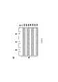
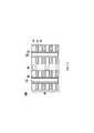
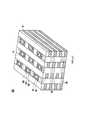
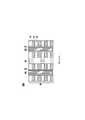
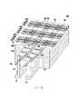
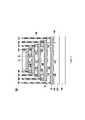
圖1A、圖1B及圖1C示出根據一些實施例的記憶體陣列的實例。圖1A以三維視圖示出記憶體陣列200的一部分的實例;圖1B示出記憶體陣列200的電路圖;且圖1C示出根據一些實施例的記憶體陣列200的俯視圖(例如,平面圖)。記憶體陣列200包括多個記憶胞202,所述多個記憶胞202可排列成列(row)與行(column)的柵格(grid)。記憶胞202可進一步垂直地堆疊以提供三維記憶體陣列,進而增大裝置密度。記憶體陣列200可設置於半導體晶粒的後段製程(back end of line,BEOL)中。舉例而言,記憶體陣列可設置於半導體晶粒的內連層中,例如設置於形成於半導體基底上的一或多個主動裝置(例如,電晶體等)上方。1A, 1B, and 1C illustrate examples of memory arrays in accordance with some embodiments. 1A shows an example of a portion of
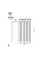
在一些實施例中,記憶體陣列200是非揮發性記憶體陣列,例如或非(NOR)記憶體陣列等。每一記憶胞202可包括具有作為閘極介電質的絕緣記憶體膜90的電晶體204。在一些實施例中,電晶體204可為薄膜電晶體(thin film transistor,TFT)。在一些實施例中,每一電晶體204的閘極電性耦合至相應的字元線(例如,導電線72),每一電晶體204的第一源極/汲極區電性耦合至相應的位元線(例如,導電線106),且每一電晶體204的第二源極/汲極區電性耦合至相應的源極線(例如,導電線108),所述源極線將第二源極/汲極區電性耦合至接地(ground)。記憶體陣列200的同一水平列中的記憶胞202可共享字元線(例如,導電線72),而記憶體陣列200的同一垂直行中的記憶胞202可共享共用源極線(例如,導電線108)及共用位元線(例如,導電線106)。In some embodiments, the
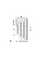
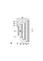
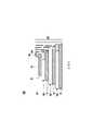
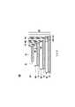
記憶體陣列200包括多條垂直堆疊的導電線72(例如,字元線),其中在導電線72中的相鄰的導電線72之間設置有空氣隙132。導電線72在與下伏基底(未在圖1A及圖1B中單獨示出)的主表面平行的方向上延伸。導電線72可具有階梯(或台階)配置(staircase configuration),使得下部的導電線72長於上部的導電線72且在側向上延伸超過上部的導電線72的端點。舉例而言,如圖1A中所示,導電線72的多個堆疊層被示出為最頂部導電線72是最短的且最底部導電線72是最長的。導電線72的相應的長度可在朝向下伏基底的方向上增大。以此種方式,可自記憶體陣列200上方觸及導電線72中的每一者的一部分,且可製成多個導電接觸件,其接觸至導電線72中的每一者的被暴露出的部分(參見例如圖31A至圖31D)。每一空氣隙132可在一端或兩端處被由介電材料形成的密封件140密封。The
記憶體陣列200更包括多條導電線106(例如,位元線)及多條導電線108(例如,源極線)。導電線106及導電線108可各自在與導電線72垂直的方向上延伸。在導電線106及導電線108中的相鄰的導電線106與導電線108之間設置有介電材料98且介電材料98將所述相鄰的導電線106與導電線108隔離開。多對的導電線106及導電線108與相交的導電線72一起界定每一記憶胞202的邊界,並且在相鄰的導電線106及導電線108對之間設置有介電材料102且介電材料102將所述的多對中的相鄰的導電線106及導電線108隔離開。在一些實施例中,導電線108電性耦合至接地。儘管圖1A示出導電線106相對於導電線108的特定放置,然而應理解,在其他實施例中可對導電線106及導電線108的放置進行翻轉。The
如上所述,記憶體陣列200亦可包括氧化物半導體(oxide semiconductor,OS)層92。氧化物半導體層92可為具有多個記憶胞202的電晶體204提供通道區。舉例而言,當藉由對應的導電線72施加適當的電壓(例如,高於對應的電晶體204的相應的臨限電壓(Vth))時,與導電線72相交的氧化物半導體層92的區域可使得電流能夠自導電線106流動至導電線108(例如,在箭頭207所指示的方向上)。因此,在一些情況下,氧化物半導體層92可被認為是通道層。As described above, the
記憶體膜90設置於導電線72與氧化物半導體層92之間,且記憶體膜90可為電晶體204提供閘極介電質。在一些實施例中,記憶體膜90包含鐵電材料,例如氧化鉿、氧化鉿鋯、摻雜矽的氧化鉿等。因此,記憶體陣列200亦可被稱為鐵電隨機存取記憶體(FeRAM)陣列。作為另外一種選擇,記憶體膜90可為多層結構,所述多層結構包括位於兩個SiOx層之間的SiNx層(例如,ONO結構)、不同的鐵電材料、不同類型的記憶體層(例如,能夠儲存位元)等。The
在其記憶體膜90包含鐵電材料的一些實施例中,記憶體膜90可在兩個不同的方向中的一個方向上極化,且可藉由在記憶體膜90兩端施加適當的電壓差動(voltage differential)且產生適當的電場來改變極化方向(polarization direction)。極化可相對地局部化(例如,一般而言包含於記憶胞202的每一邊界內),且記憶體膜90的連續的區域可延伸跨越多個記憶胞202。依據記憶體膜90的特定區的極化方向而定,對應的電晶體204的臨限電壓會發生變化,且可儲存數位值(例如,0或1)。舉例而言,當記憶體膜90的區域具有第一電性極化方向時,所述對應的電晶體204可具有相對低的臨限電壓,且當記憶體膜90的區域具有第二電性極化方向時,所述對應的電晶體204可具有相對高的臨限電壓。所述兩個臨限電壓之間的差可被稱為臨限電壓偏移(threshold voltage shift)。較大的臨限電壓偏移使得讀取儲存於對應的記憶胞202中的數位值更容易(例如,更不容易出現錯誤)。In some embodiments in which the
在此種實施例中,為對記憶胞202執行寫入操作(write operation),在與記憶胞202對應的記憶體膜90的一部分兩端施加寫入電壓。可例如藉由向對應的導電線72(例如,字元線)及對應的導電線106及導電線108(例如,位元線/源極線)施加適當的電壓來施加寫入電壓。藉由在記憶體膜90的所述部分兩端施加寫入電壓,可改變記憶體膜90的區域的極化方向。因此,所述對應的電晶體204的對應的臨限電壓可自低臨限電壓切換至高臨限電壓或者可自高臨限電壓切換至低臨限電壓,且數位值(digital value)可被儲存於記憶胞202中。由於導電線72與導電線106及導電線108相交,因此可選擇各別的記憶胞202來進行寫入操作。In such an embodiment, in order to perform a write operation on the
在此種實施例中,為對記憶胞202執行讀取操作(read operation),向對應的導電線72(例如,字元線)施加讀取電壓(低臨限電壓與高臨限電壓之間的電壓)。依據記憶體膜90的對應區域的極化方向而定,可接通或可不接通記憶胞202的電晶體204。因此,可藉由或可不藉由導電線108(例如,耦合至接地的源極線)對導電線106進行放電,且可確定儲存於記憶胞202中的數位值。由於導電線72與導電線106及導電線108相交,因此可選擇各別的記憶胞202以進行讀取操作。In such an embodiment, to perform a read operation on the
圖1A進一步示出在後面的圖中使用的記憶體陣列200的參考橫截面。參考橫截面B-B’是沿著導電線72的縱向軸線(longitudinal axis)且位於例如與電晶體204的電流流動的方向平行的方向上。參考橫截面C-C’垂直於參考橫截面B-B’且平行於導電線72的縱向軸線。參考橫截面C-C’延伸穿過導電線106及/或導電線108。參考橫截面D-D’平行於參考橫截面C-C’且延伸穿過介電材料102。為清晰起見,後續的圖是指該些參考橫截面。FIG. 1A further shows a reference cross-section of
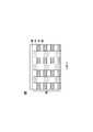
在圖2中,提供基底50。基底50可為半導體基底(例如塊狀半導體、絕緣體上有半導體(semiconductor-on-insulator,SOI)基底等),所述半導體基底可為經摻雜的(例如,使用p型摻雜劑或n型摻雜劑)或未經摻雜的。基底50可為晶圓,例如矽晶圓。一般而言,SOI基底是形成於絕緣體層上的半導體材料層。絕緣體層可為例如隱埋式氧化物(buried oxide,BOX)層、氧化矽層等。絕緣體層設置於基底(通常是矽基底或玻璃基底)上。亦可使用其他基底,例如多層式基底(multi-layered substrate)或梯度基底(gradient substrate)。在一些實施例中,基底50的半導體材料可包括:矽;鍺;化合物半導體,包括碳化矽、砷化鎵、磷化鎵、磷化銦、砷化銦及/或銻化銦;合金半導體,包括矽-鍺、砷磷化鎵、砷化鋁銦、砷化鋁鎵、砷化鎵銦、磷化鎵銦及/或砷磷化鎵銦;或其組合。In Figure 2, a
圖2進一步示出可在基底50之上形成多個電路。所述多個電路包括位於基底50的頂表面處的多個主動裝置(例如,多個電晶體)。所述多個電晶體可包括位於基底50的頂表面之上的閘極介電層203及位於閘極介電層203之上的多個閘極電極205。在基底50中在閘極介電層203及閘極電極205的相對的側上設置多個源極/汲極區206。沿著閘極介電層203的側壁形成多個閘極間隔件208且閘極間隔件208將源極/汲極區206與閘極電極205隔開適當的側向距離。在一些實施例中,電晶體可為平面場效電晶體(planar field effect transistor,FET)、鰭場效電晶體(fin field effect transistor,FinFET)、奈米場效電晶體(nano-field effect transistor,nanoFET)等。FIG. 2 further shows that a plurality of circuits may be formed over
第一層間介電質(inter-layer dielectric,ILD)210環繞源極/汲極區206、閘極介電層203及閘極電極205且將源極/汲極區206、閘極介電層203及閘極電極205隔離開,且第二層間介電質212位於第一層間介電質210之上。多個源極/汲極接觸件214延伸穿過第二層間介電質212及第一層間介電質210且電性耦合至源極/汲極區206,且多個閘極接觸件216延伸穿過第二層間介電質212且電性耦合至閘極電極205。在第二層間介電質212、源極/汲極接觸件214及閘極接觸件216之上存在包括堆疊的一或多個介電層224及形成於所述一或多個介電層224中的多個導電特徵222的內連結構220。儘管圖2示出堆疊的兩個介電層224,但應理解內連結構220可包括任意數目的其中設置有導電特徵222的介電層224。內連結構220可電性連接至閘極接觸件216及源極/汲極接觸件214,以形成功能電路。在一些實施例中,由內連結構220形成的功能電路可包括邏輯電路、記憶體電路、感測放大器、控制器、輸入/輸出電路、影像感測器電路、類似電路或其組合。儘管圖2論述了形成於基底50之上的電晶體,然而亦可形成其他主動裝置(例如,二極體等)及/或被動裝置(例如,電容器、電阻器等)作為功能電路的部件。Surrounded by a first inter-layer dielectric (ILD) 210The source/
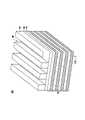
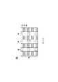
在圖3A及圖3B中,在圖2所示結構之上形成多層堆疊58。出於簡潔及清晰的目的,基底50、電晶體、層間介電質及內連結構220可自隨後的附圖中省略。儘管多層堆疊58被示出為與內連結構220的介電層224接觸,然而可在基底50與多層堆疊58之間設置任意數目的中間層。舉例而言,可在基底50與多層堆疊58之間設置包括位於絕緣層(例如,低介電常數(low-k)介電層)中的多個導電特徵的一或多個附加內連層。在一些實施例中,可將所述多個導電特徵圖案化以為基底50及/或記憶體陣列200(參見圖1A及圖1B)上的主動裝置提供電源線、接地線及/或訊號線。In FIGS. 3A and 3B , a
多層堆疊58包括具有導電層54A至導電層54D(統稱為導電層54)與犧牲層52A至犧牲層52C(統稱為犧牲層52)的多個交替層。多層堆疊58包括位於最頂部導電層54之上的絕緣層74。在後續步驟中可將導電層54圖案化以界定導電線72(例如,字元線)。導電層54可包含導電材料,例如銅、鈦、氮化鈦、鉭、氮化鉭、鎢、釕、鋁、其組合。犧牲層52可為例如矽、鍺、矽鍺(SiGe)、氮化矽、氧化矽、其組合等。絕緣層74可包含絕緣材料,例如氧化矽、氮化矽、氮氧化矽、其組合等。在一些實施例中,選擇絕緣層74的材料及犧牲層52的材料,使得可選擇性地蝕刻犧牲層52,而不會明顯地蝕刻絕緣層74。舉例而言,犧牲層52可為矽且絕緣層74可為氧化矽,但是其他材料是可能的。
導電層54、犧牲層52及絕緣層74可各自使用例如化學氣相沈積(chemical vapor deposition,CVD)、原子層沈積(atomic layer deposition,ALD)、物理氣相沈積(physical vapor deposition,PVD)、電漿增強型化學氣相沈積(plasma enhanced CVD,PECVD)等形成。在一些實施例中,犧牲層52被形成為具有處於約20奈米至約80奈米的範圍內的厚度T0。其他厚度是可能的。多層堆疊58的犧牲層52可全部具有約相同的厚度,或者犧牲層52中的兩個或兩個以上可具有不同的厚度。儘管圖3A及圖3B示出特定數目的導電層54及犧牲層52,但是其他實施例可包括不同數目的導電層54及犧牲層52。The
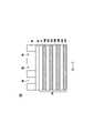
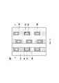
圖4至圖12是根據一些實施例的製造記憶體陣列200的階梯結構中的中間階段的視圖。圖4至圖11及圖12是沿著圖1中所示的參考橫截面B-B’示出。4-12 are views of intermediate stages in fabricating a ladder structure of
在圖4中,在多層堆疊58之上形成光阻56。如上所述,多層堆疊58可包括具有多個導電層54(標記為54A、54B、54C及54D)與多個犧牲層52(標記為52A、52B及52C)的多個交替層,且可被絕緣層74覆蓋。可藉由使用合適的技術(例如藉由旋轉塗佈技術)形成光阻56。In FIG. 4 ,
在圖5中,將光阻56圖案化以在多個區域60中暴露出多層堆疊58,同時掩蔽多層堆疊58的其餘部分。舉例而言,可在區域60中暴露出多層堆疊58的最頂部層(例如,絕緣層74)。可使用可接受的微影技術來將光阻56圖案化。In FIG. 5 ,
在圖6中,使用光阻56作為罩幕對在區域60中被暴露出的多層堆疊58的部分進行蝕刻。所述蝕刻可為任何可接受的蝕刻製程,例如藉由濕式蝕刻或乾式蝕刻、反應性離子蝕刻(reactive ion etching,RIE)、中性束蝕刻(neutral beam etching,NBE)、類似蝕刻或其組合。所述蝕刻可為非等向性的。所述蝕刻可移除位於區域60中的導電層54D及犧牲層52C的部分且界定多個開口61。由於絕緣層74、導電層54D及犧牲層52C具有不同的材料組成,因此用於移除該些層的被暴露出的部分的蝕刻劑可不同。在一些實施例中,在蝕刻導電層54D時犧牲層52C充當蝕刻停止層,且在蝕刻犧牲層52C時導電層54C充當蝕刻停止層。因此,可選擇性地移除絕緣層74、導電層54D及犧牲層52C的部分,而不移除多層堆疊58的其餘層,且開口61可延伸至期望的深度。作為另外一種選擇,在開口61達到期望的深度之後,可使用定時蝕刻製程(timed etch process)來停止對開口61的蝕刻。在所得結構中,導電層54C在區域60中被暴露出。In FIG. 6, the portion of the
在圖7中,對光阻56進行修整以暴露出多層堆疊58的多個附加部分。可使用可接受的微影技術對光阻進行修整。作為修整的結果,光阻56的寬度減小且暴露出位於區域60及區域62中的多層堆疊58的部分。舉例而言,可在區域60中暴露出導電層54C的頂表面,且可在區域62中暴露出絕緣層74的頂表面。In FIG. 7 ,
在圖8中,藉由可接受的蝕刻製程,使用光阻56作為罩幕移除位於區域60及區域62中的絕緣層74、導電層54D、犧牲層52C、導電層54C及犧牲層52B的部分。所述蝕刻可為任何可接受的蝕刻製程,例如藉由濕式蝕刻或乾式蝕刻、反應性離子蝕刻(RIE)、中性束蝕刻(NBE)、類似蝕刻或其組合。所述蝕刻可為非等向性的。所述蝕刻可使所述多個開口61進一步延伸至多層堆疊58中。由於絕緣層74、導電層54D、導電層54C、犧牲層52C及犧牲層52B具有不同的材料組成,因此用於移除該些層的被暴露出的部分的蝕刻劑可不同。在一些實施例中,在蝕刻導電層54D時犧牲層52C充當蝕刻停止層;在蝕刻犧牲層52C時導電層54C充當蝕刻停止層;在蝕刻導電層54C時犧牲層52B充當蝕刻停止層;且在蝕刻犧牲層52B時導電層54B充當蝕刻停止層。因此,可選擇性地移除導電層54D、導電層54C及犧牲層52C、犧牲層52B的部分,而不移除多層堆疊58的其餘層,且開口61可延伸至期望的深度。此外,在蝕刻製程期間,導電層54及犧牲層52的未被蝕刻的部分充當下伏膜層的罩幕,且因此導電層54D及犧牲層52C的先前圖案(參見圖7)可被轉移至下伏的導電層54C及犧牲層52B。在所得結構中,導電層54B在區域60中被暴露出,且導電層54C在區域62中被暴露出。In FIG. 8, insulating
在圖9中,對光阻56進行修整以暴露出多層堆疊58的多個附加部分。可使用可接受的微影技術對光阻進行修整。作為修整的結果,光阻56的寬度減小且暴露出多層堆疊58的位於區域60、區域62、及區域64中的部分。舉例而言,可在區域60中暴露出導電層54B的頂表面;可在區域62中暴露出導電層54C的頂表面;且可在區域64中暴露出絕緣層74的頂表面。In FIG. 9 ,
在圖10中,藉由可接受的蝕刻製程,使用光阻56作為罩幕移除位於區域64中的絕緣層74的部分以及位於區域60、區域62及區域64中的導電層54D、導電層54C及導電層54B的部分。所述蝕刻可為任何可接受的蝕刻製程,例如藉由濕式蝕刻或乾式蝕刻、反應性離子蝕刻(RIE)、中性束蝕刻(NBE)、類似蝕刻或其組合。所述蝕刻可為非等向性的。所述蝕刻可使所述多個開口61進一步延伸至多層堆疊58中。在一些實施例中,在蝕刻導電層54D時犧牲層52C充當蝕刻停止層;在蝕刻導電層54C時犧牲層52B充當蝕刻停止層;且在蝕刻導電層54B時犧牲層52A充當蝕刻停止層。因此,可選擇性地移除導電層54D、導電層54C及導電層54B的部分,而不移除多層堆疊58的其餘層,且開口61可延伸至期望的深度。此外,在蝕刻製程期間,犧牲層52中的每一者充當下伏層的罩幕,且因此犧牲層52C、犧牲層52B的先前圖案(參見圖9)可被轉移至下伏的導電層54C、導電層54B。在所得結構中,犧牲層52A在區域60中被暴露出;犧牲層52B在區域62中被暴露出;且犧牲層52C在區域64中被暴露出。In FIG. 10, portions of insulating
在圖11中,可例如藉由可接受的灰化製程(ashing process)或濕式剝除製程(wet strip process)移除光阻56。因此形成階梯結構68。階梯結構68包括具有多個導電層54及多個犧牲層52的多個交替層的堆疊,其中頂部導電層(例如,導電層54D)被絕緣層74覆蓋。下部導電層54較上部導電層54寬且在側向上延伸超過上部導電層54,且導電層54中的每一者的寬度在朝向基底50的方向上增大。舉例而言,導電層54A可長於導電層54B;導電層54B可長於導電層54C;且導電層54C可長於導電層54D。因此,在隨後的處理步驟中,可自階梯結構68上方至導電層54中的每一者製成導電接觸件。In FIG. 11,
在圖12中,在多層堆疊58之上沈積金屬間介電層(inter-metal dielectric layer,IMD)70。金屬間介電層70可由介電材料形成且可藉由任何合適的方法(例如CVD、電漿增強型CVD(PECVD)、或可流動化學氣相沈積(flowable CVD,FCVD))沈積。介電材料可包括磷矽酸鹽玻璃(phospho-silicate glass,PSG)、硼矽酸鹽玻璃(boro-silicate glass,BSG)、摻雜硼的磷矽酸鹽玻璃(boron-doped phospho-silicate glass,BPSG)、未經摻雜的矽酸鹽玻璃(undoped silicate glass,USG)等。可使用藉由任何可接受的製程形成的其他隔離材料。金屬間介電層70沿著絕緣層74的側壁、導電層54的側壁及犧牲層52的側壁延伸。此外,金屬間介電層70可接觸犧牲層52中的每一者的頂表面。In FIG. 12 , an inter-metal dielectric layer (IMD) 70 is deposited over the
如圖12中進一步所示,可對金屬間介電層70執行移除製程,以移除多層堆疊58之上的多餘介電材料。在一些實施例中,可利用平坦化製程(例如化學機械拋光(chemical mechanical polish,CMP)、研磨製程、回蝕製程、其組合等)。平坦化製程暴露出多層堆疊58,使得在平坦化製程完成之後,多層堆疊58的頂表面(例如,絕緣層74的頂表面)與金屬間介電層70的頂表面齊平。As further shown in FIG. 12 , a removal process may be performed on the
圖13至圖19B是根據一些實施例的製造記憶體陣列200中的中間階段的視圖。在圖13至圖19B中,形成多層堆疊58,且在多層堆疊58中形成多個溝渠,藉此界定多個導電線72。導電線72可對應於記憶體陣列200中的字元線,且導電線72可進一步為記憶體陣列200的所得電晶體提供多個閘極電極。圖14A、圖17A及圖19A是以三維視圖示出。圖13、圖14B、圖15、圖16、圖17B、圖18及圖19B是沿著圖1A中所示的參考橫截面C-C’示出。13-19B are views of intermediate stages in the fabrication of
在圖13中,在多層堆疊58之上沈積硬罩幕80及光阻82。硬罩幕80可包括例如氮化矽、氮氧化矽等,硬罩幕80可藉由CVD、PVD、ALD、PECVD等來沈積。舉例而言,光阻82可例如藉由使用旋轉塗佈技術來形成。In FIG. 13 , a
在圖14A及圖14B中,將光阻82圖案化以形成多個溝渠86。可使用可接受的微影技術來將光阻82圖案化。舉例而言,光阻82可被暴露至光,以用於圖案化。在曝光製程之後,可依據使用的是負性抗蝕劑亦或正性抗蝕劑而定來對光阻82進行顯影以移除光阻82的被暴露出的部分或未被暴露出的部分,藉此界定溝渠86的圖案。In FIGS. 14A and 14B ,
在圖15中,使用可接受的蝕刻製程(例如藉由濕式蝕刻或乾式蝕刻、反應性離子蝕刻(RIE)、中性束蝕刻(NBE)、類似蝕刻或其組合)將光阻82的圖案轉移至硬遮罩80。所述蝕刻可為非等向性的。因此,形成延伸穿過硬遮罩80的溝渠86。舉例而言,可藉由灰化製程移除光阻82。In FIG. 15, the pattern of
在圖16中,使用一或多種可接受的蝕刻製程(例如藉由濕式蝕刻或乾式蝕刻、反應性離子蝕刻(RIE)、中性束蝕刻(NBE)、類似蝕刻或其組合)將硬遮罩80的圖案轉移至多層堆疊58。所述蝕刻製程可為非等向性的。因此,溝渠86穿過多層堆疊58延伸,且多個導電線72(例如,字元線)由導電層54形成。藉由蝕刻溝渠86穿過導電層54,可將相鄰的導電線72彼此隔開。隨後,在圖17A及圖17B中,然後可藉由可接受的製程(例如濕式蝕刻製程、乾式蝕刻製程、平坦化製程、其組合等)移除硬遮罩80。由於多層堆疊58的階梯形狀(例如,參見圖12),導電線72可具有在朝向基底50的方向上增加的不同長度。舉例而言,導電線72A可長於導電線72B;導電線72B可長於導電線72C;且導電線72C可長於導電線72D。在一些實施例中,溝渠86可被形成為具有處於約50奈米至約100奈米的範圍內的寬度W1,儘管其他寬度是可能的。16, the hardmask is The pattern of
在圖18中,在溝渠86的側壁及底表面上沈積介電材料98。介電材料98可包括例如氧化矽、氮化矽、氮氧化矽等,介電材料98可藉由CVD、PVD、ALD、PECVD等來沈積。如圖18中所示,介電材料98可填充溝渠86且可覆蓋多層堆疊58。In FIG. 18 , a
在圖19A及圖19B中,然後進行移除製程,以移除多層堆疊58之上的多餘介電材料98。在一些實施例中,可利用平坦化製程(例如化學機械拋光(CMP)、研磨製程、回蝕製程、其組合等)。平坦化製程可暴露出多層堆疊58,使得在平坦化製程完成之後多層堆疊58的頂表面(例如,絕緣層74的頂表面)是齊平的。圖19A示出三維視圖,且圖19B示出穿過圖1A中所示的參考橫截面C-C’的剖視圖。In FIGS. 19A and 19B , a removal process is then performed to remove excess
在圖20A、圖20B及圖20C中,穿過介電材料98圖案化出多個溝渠88。圖20A以三維視圖示出。圖20B以平面圖示出。圖20C是以沿著圖1A的參考橫截面C-C’的剖視圖示出。溝渠88可設置於多層堆疊58的相對側壁之間,且界定隨後形成有部分的電晶體的區域。在一些實施例中,可藉由微影與蝕刻的組合來執行溝渠88的圖案化。舉例而言,可在多層堆疊58之上沈積光阻。舉例而言,可藉由使用合適的技術(例如旋轉塗佈技術)形成光阻。然後可將光阻圖案化以界定暴露出介電材料98的區域的多個開口。可使用可接受的微影技術將光阻圖案化。舉例而言,光阻可被暴露至光,以用於圖案化,且在曝光製程之後,可依據使用的是負性抗蝕劑亦或正性抗蝕劑而定來對光阻進行顯影以移除光阻的被暴露出的部分或未被暴露出的部分,藉此界定開口的圖案。In FIGS. 20A , 20B, and 20C, a plurality of
介電材料98被開口122暴露出的部分可藉由蝕刻來移除,以在介電材料98中形成溝渠88。所述蝕刻可為任何可接受的蝕刻製程,例如藉由濕式蝕刻或乾式蝕刻、反應性離子蝕刻(RIE)、中性束蝕刻(NBE)、類似蝕刻或其組合。所述蝕刻可為非等向性的。在一些實施例中,溝渠88可具有處於約80奈米至約150奈米的範圍內的長度L1,儘管其他尺寸是可能的。在一些實施例中,溝渠88由處於約30奈米至約120奈米的範圍內的距離L2隔開,儘管其他距離是可能的。在一些實施例中,溝渠88可具有處於約1000奈米至約2000奈米的範圍內的深度,儘管其他深度是可能的。在溝渠88被圖案化之後,可藉由例如灰化來移除光阻。在一些情況下,溝渠88在平面圖中的形狀可為如圖20B中所示的矩形,或者可為經圓化的矩形形狀或是圓的形狀(例如橢圓或圓形形狀)。Portions of
在圖21中,在溝渠88中共形地沈積記憶體膜90。記憶體膜90可包括能夠儲存位元的材料,例如能夠藉由在記憶體膜90兩端施加適當的電壓差來在兩個不同的極化方向之間進行切換的材料。舉例而言,記憶體膜90的極化可能由於施加電壓差產生的電場而改變。在一些實施例中,記憶體膜90包含高介電常數(high-k)介電材料,例如鉿(Hf)系介電材料等。在一些實施例中,記憶體膜90包含鐵電材料,例如氧化鉿、氧化鉿鋯、摻雜矽的氧化鉿等。在其他實施例中,記憶體膜90可為包括位於兩個SiOx層之間的SiNx層(例如,ONO結構)的多層結構。在又一些其他實施例中,記憶體膜90包含不同的鐵電材料或不同類型的記憶體材料。記憶體膜90可藉由CVD、PVD、ALD、PECVD等進行沈積,以沿著溝渠88的側壁及底表面延伸。在一些實施例中,在沈積記憶體膜90之後,可執行退火步驟。在一些實施例中,記憶體膜90可沈積至處於約5奈米至約15奈米的範圍內的厚度,儘管其他厚度是可能的。In FIG. 21 , the
在圖22中,在記憶體膜90之上在溝渠88中共形地沈積氧化物半導體層92。氧化物半導體層92包括適於為電晶體(例如,電晶體204,參見圖1A)提供通道區的材料。在一些實施例中,氧化物半導體層92包含含銦材料(例如InxGayZnzMO),其中M可為Ti、Al、Sn、W等。X、Y及Z可各自為0與1之間的任何值。舉例而言,氧化物半導體層92可包含氧化銦鎵鋅、氧化銦鈦、氧化銦鎢、氧化銦、類似材料或其組合。在其他實施例中,不同於該些實例的半導體材料可用於氧化物半導體層92。氧化物半導體層92可藉由CVD、PVD、ALD、PECVD等沈積。氧化物半導體層92可在溝渠88內沿著記憶體膜90的側壁及沿著底表面延伸。在一些實施例中,在沈積氧化物半導體層92之後,可在與氧相關的環境中執行退火步驟(例如,處於約300℃至約450℃的溫度範圍內),以激活氧化物半導體層92的電荷載流子。在一些實施例中,氧化物半導體層92可沈積至處於約1奈米至約15奈米的範圍內的厚度,儘管其它厚度是可能的。In FIG. 22 , an
在圖23A、圖23B及圖23C中,根據一些實施例,在氧化物半導體層92之上沈積介電材料102並填充溝渠88。圖23C示出圖23B中的線C-C’的剖視圖。介電材料102可包括例如氧化矽、氮化矽、氮氧化矽、類似材料或其組合。介電材料102的材料可與介電材料98的材料相同或不同。介電材料102可使用合適的技術(例如CVD、PVD、ALD、PECVD等)沈積。介電材料102可在溝渠88內沿著氧化物半導體層92的側壁及沿著底表面延伸。在沈積之後,可執行平坦化製程(例如,CMP、回蝕等)以移除介電材料102的多餘部分。在所得結構中,多層堆疊58的頂表面、記憶體膜90的頂表面、氧化物半導體層92的頂表面及介電材料102的頂表面可實質上齊平。In FIGS. 23A, 23B, and 23C,
圖24A至圖25C示出在記憶體陣列200中製造多個導電線106及多個導電線108(例如,源極線及位元線)的中間步驟。導電線106及導電線108可沿著垂直於導電線72的方向延伸,使得記憶體陣列200的各別胞元可被選擇用於進行讀取及寫入操作。圖24A及圖25A示出三維視圖。圖24B及圖25B示出俯視圖。圖24C及圖25C示出沿著圖1A中及例如圖25B中所示的參考橫截面C-C’的剖視圖。FIGS. 24A-25C illustrate intermediate steps in the fabrication of the plurality of
在圖24A、圖24B及圖24C中,根據一些實施例,在介電材料102中圖案化出多個溝渠120。藉由使用微影與蝕刻的組合對介電材料102進行圖案化來圖案化出溝渠120。舉例而言,可在多層堆疊58、介電材料98、氧化物半導體層92及記憶體膜90以及介電材料102之上沈積光阻。舉例而言,可藉由使用旋轉塗佈技術形成光阻。將光阻圖案化以界定多個開口。所述多個開口中的每一者可與介電材料102的對應區重疊。開口不與介電材料102完全重疊,且與開口不重疊的介電材料102的部分界定相鄰的導電線106與導電線108之間的隔離區。可使用可接受的微影技術來圖案化光阻。舉例而言,光阻可被暴露至光,以用於圖案化。在曝光製程之後,可依據使用的是負性抗蝕劑亦或正性抗蝕劑而定來對光阻進行顯影以移除光阻的被暴露出的部分或未被暴露出的部分,藉此界定開口。In FIGS. 24A, 24B, and 24C, a plurality of
介電材料102被開口暴露出的部分可藉由蝕刻來移除,以形成溝渠120。所述蝕刻可為任何可接受的蝕刻製程,例如藉由濕式蝕刻或乾式蝕刻、反應性離子蝕刻(RIE)、中性束蝕刻(NBE)、類似蝕刻或其組合。所述蝕刻可為非等向性的。以此種方式,溝渠120可界定形成有導電線106及導電線108的區域的圖案。圖24C示出其中在形成溝渠120之後氧化物半導體層92保留在記憶體膜90之上的實施例。在其他實施例中,蝕刻可移除氧化物半導體層92的側壁部分及/或底部部分,此可暴露出記憶體膜90。在溝渠120被圖案化之後,可藉由例如灰化來移除光阻。在一些情況下,溝渠120在平面圖中的形狀可為如圖24B中所示的矩形,或者可為經圓化的矩形形狀或圓的形狀(例如橢圓或圓形形狀)。Portions of
在圖25A、圖25B及圖25C中,根據一些實施例,溝渠120填充有導電材料,以形成導電線106及導電線108。導電材料可包括一或多種材料,例如銅、鈦、氮化鈦、鉭、氮化鉭、鎢、釕、鋁、鉬、其組合等,所述導電材料可各自使用例如CVD、ALD、PVD、PECVD等形成。在沈積導電材料之後,可執行平坦化製程以移除導電材料的多餘部分。在所得結構中,多層堆疊58的頂表面、記憶體膜90的頂表面、氧化物半導體層92的頂表面、絕緣層74的頂表面、及導電線106與導電線108的頂表面可實質上齊平(例如,在製程變化內共面)。In FIGS. 25A, 25B, and 25C,
導電線106可對應於記憶體陣列200中的位元線,且導電線108可對應於記憶體陣列200中的源極線。儘管圖25C示出僅示出導電線108的剖視圖,但是導電線106的剖視圖可為相似的。相鄰的導電線106與導電線108被由介電材料102形成的隔離區隔開。
以此種方式,可在記憶體陣列200中形成堆疊的多個電晶體204。每一電晶體204包括閘極電極(例如,對應的導電線72的一部分)、閘極介電質(例如,對應的記憶體膜90的一部分)、通道區(例如,對應的氧化物半導體層92的一部分)、以及源極及汲極電極(例如,對應的導電線106及108的一部分)。介電材料102將同一行中的相鄰的電晶體204隔離在相同的垂直水準處。電晶體204可設置於垂直堆疊的列與行的陣列中。In this manner, a stacked plurality of
圖26A至圖30示出根據一些實施例的製造導電線72之間的空氣隙132的中間步驟。藉由移除犧牲層52而在垂直相鄰的導電線72之間形成空氣隙132,此將在以下更詳細地闡述。藉由使用空氣隙132代替犧牲層52,可減小導電線72之間的電容,此可改善電晶體的速度及效能,特別是在較高的運作頻率下。在圖26A至圖30中闡述的製程中,使用相同的製程步驟形成多個空氣隙132。在其他實施例中,空氣隙132可藉由重複用於形成每一空氣隙132的相似製程步驟來順序形成。26A-30 illustrate intermediate steps in fabricating
在圖26A至圖26B中,形成多個溝渠130以暴露出犧牲層52。溝渠130容許移除多個犧牲層52、形成多個密封件140(參見圖28)及形成多個接觸件(又稱導電接觸件)110。在一些實施例中,溝渠130可延伸穿過犧牲層52以暴露出下伏的導電線72,如圖26A中所示。在其他實施例中,溝渠130可暴露出犧牲層52,而不暴露出導電線72。舉例而言,溝渠130可暴露出犧牲層52的頂表面,如圖26B中所示。溝渠130可被形成為暴露出每一犧牲層52的一個區域,如圖26A至圖26B中所示,或者每一犧牲層52的多個區域可被多個溝渠130暴露出。在每一犧牲層52的兩端上形成有溝渠130的實例在以下圖33中示出。In FIGS. 26A-26B , a plurality of
可藉由使用微影與蝕刻的組合在金屬間介電層70中圖案化出多個開口來形成溝渠130。作為實例,可在多層堆疊58及金屬間介電層70之上沈積光阻。舉例而言,可藉由使用旋轉塗佈技術形成光阻。可使用可接受的微影技術來圖案化光阻以界定出多個開口。舉例而言,光阻可被暴露至光,以用於圖案化。在曝光製程之後,可依據使用的是負性抗蝕劑亦或正性抗蝕劑而定來對光阻進行顯影以移除光阻的被暴露出的部分或未被暴露出的部分,藉此界定開口。The
金屬間介電層70被開口暴露出的部分可藉由蝕刻來移除,以形成溝渠130。所述蝕刻可為任何可接受的蝕刻製程,例如藉由濕式蝕刻或乾式蝕刻、反應性離子蝕刻(RIE)、中性束蝕刻(NBE)、類似蝕刻或其組合。所述蝕刻可為非等向性的。在一些實施例中,金屬間介電層70中的多個開口可延伸穿過犧牲層52以形成暴露出導電線72的溝渠130,如圖26A中所示。在該些實施例中,可使用相同的蝕刻步驟或不同的蝕刻步驟來蝕刻金屬間介電層70及犧牲層52。舉例而言,可使用第一蝕刻製程來蝕刻金屬間介電層70,且可使用不同於第一蝕刻製程的第二蝕刻製程來蝕刻犧牲層52。在一些實施例中,第二蝕刻製程亦可移除犧牲層52以形成多個空氣隙132,此將在以下更詳細地闡述。在一些實施例中,第二蝕刻製程可選擇性地蝕刻犧牲層52。在溝渠130被圖案化之後,可藉由例如灰化來移除光阻。The portion of the
在圖27中,根據一些實施例,使用蝕刻製程移除犧牲層52以在導電層54之間形成空氣隙132。在一些實施例中,如上所述,移除犧牲層52的蝕刻製程可作為形成溝渠130的一部分來執行。換言之,移除犧牲層52的蝕刻製程可在形成溝渠130期間或在形成溝渠130之後執行。移除犧牲層52的蝕刻製程可在移除用於圖案化溝渠130的光阻之前或之後執行。在一些實施例中,空氣隙132被形成為具有處於約20奈米至約80奈米的範圍內的高度H0。其他高度是可能的。空氣隙132的高度H0可與對應的犧牲層52的厚度T0大致相同。在一些實施例中,空氣隙132的高度沿著其長度而變化,此將在以下針對圖35更詳細地闡述。空氣隙132可均具有大致相同的高度,或者空氣隙132中的兩者或兩者以上可具有不同的高度。In FIG. 27,
移除犧牲層52的蝕刻製程可包括一或多個乾蝕刻製程及/或一或多個濕式蝕刻製程。溝渠130容許蝕刻製程的蝕刻劑(例如,製程氣體、電漿、濕式蝕刻劑等)到達並蝕刻犧牲層52的被暴露出的表面。在一些實施例中,電漿蝕刻製程使用製程氣體,例如O2、CF4、CHF3、C4F8、BCl3、CCl4、Cl2、SF6、HBr、H2、其組合等。其他製程氣體是可能的。在一些實施例中,製程氣體以處於約5每分鐘標準立方公分(sccm)至約50每分鐘標準立方公分的範圍內的速率流動。在一些實施例中,電漿蝕刻製程在處於約200℃至約450℃的範圍內的製程溫度下及在處於約0.1毫托(mTorr)至約100毫托的範圍內的製程壓力下執行。在一些實施例中,電漿蝕刻製程使用處於約50瓦(W)至約500瓦的範圍內的電漿功率執行,且使用處於約50瓦至約500瓦的範圍內的偏置功率執行。其他乾式蝕刻製程或製程參數是可能的。The etching process for removing the
在一些實施例中,濕式蝕刻製程包括蝕刻劑,例如稀釋的氫氟酸(diluted hydrofluoric acid,dHf);氫氧化鉀(KOH)溶液;氫氧化氨(NH4OH);包含HF、硝酸(HNO3)及/或乙酸(CH3COOH,或稱醋酸)的溶液;其組合等。其他蝕刻劑是可能的。濕式蝕刻製程可以合適的方式進行,例如藉由在蝕刻劑中浸泡一段持續時間(例如,少於一小時等)。其他濕式蝕刻製程是可能的。在一些實施例中,藉由執行乾式蝕刻製程且然後執行濕式蝕刻製程來移除犧牲層52。在一些實施例中,在移除犧牲層52之後,執行濕式清潔製程。In some embodiments, the wet etching process includes an etchant, such as dilute hydrofluoric acid (dHf); potassium hydroxide (KOH) solution; ammonium hydroxide (NH4 OH); including HF, nitric acid ( HNO3 ) and/or acetic acid (CH3 COOH, or acetic acid) solution; combinations thereof, etc. Other etchants are possible. The wet etch process can be performed in a suitable manner, such as by soaking in an etchant for a duration (eg, less than one hour, etc.). Other wet etch processes are possible. In some embodiments, the
根據一些實施例,在圖28中,空氣隙132至少部分地填充有密封材料134。密封材料134被沈積成部分地延伸至空氣隙132中,以密封空氣隙132。以此種方式密封空氣隙132來保護空氣隙132在隨後的處理步驟中不被填充,並提供附加的結構支撐。另外,密封空氣隙132,以將空氣隙132與隨後形成的接觸件110隔離開,如下所述。圖28將密封材料134示出為部分地填充溝渠130,但是在其他實施例中,密封材料134完全填充溝渠130。在一些實施例中,密封材料134被沈積至足以密封空氣隙132的厚度,但並不填充溝渠130。在一些情況下,密封材料134可存在於溝渠130的側壁上,而不填充溝渠130,如圖28中所示。密封材料134可沿著溝渠130的側壁及沿著底表面延伸。密封材料134可在金屬間介電層70的表面及/或藉由移除犧牲層52而暴露出的導電線72的表面上延伸。沈積在空氣隙132內及溝渠130內的密封材料134的相對厚度或量可不同於圖28中所示,且其變化被認為處於本揭露的範圍內。如以下針對圖33所示及所述,延伸至空氣隙132中的密封材料134的部分可具有如圖28中所示的實質上平的側壁(flat sidewall)、可具有凹陷側壁(concave sidewall)或可具有凸出側壁(convex sidewall)。在一些情況下,密封材料134可包含空隙(void)(圖中未示出)。In FIG. 28 ,
密封材料134可包括例如氧化矽、氮化矽、氮氧化矽、類似材料或其組合。密封材料134的材料可與金屬間介電層70的材料相同或不同。密封材料134可使用合適的技術(例如CVD、PVD、ALD、PECVD等)沈積。舉例而言,在一些實施例中,密封材料134可為使用PECVD製程沈積的氧化矽。對於前驅物,PECVD製程可使用例如二氯矽烷(dichorosilane)、矽烷(silane)、氧氣(oxygen)、其組合等。在一些實施例中,PECVD製程的前驅物以處於約5每分鐘標準立方公分至約50每分鐘標準立方公分的範圍內的速率流動。在一些實施例中,PECVD製程是在處於約150℃至約350℃的範圍內的製程溫度下以及在處於約0.1毫托至約100毫托的範圍內的製程壓力下執行。在一些實施例中,使用處於約5瓦至約500瓦的範圍內的電漿功率來執行PECVD製程。此為一個實例,且其他製程參數、材料、材料組合或沈積製程是可能的。The sealing
在圖29中,根據一些實施例,執行蝕刻製程以移除密封材料134的多個多餘部分並形成多個密封件140。密封件140包含密封材料134在執行蝕刻製程後保留的部分。蝕刻製程可例如自溝渠130的側壁及/或底表面移除密封材料134的部分。在一些實施例中,蝕刻製程移除密封材料134的部分,使得下伏的導電線72被暴露出。蝕刻製程可包括乾式蝕刻製程、濕式蝕刻製程或其組合。舉例而言,蝕刻製程可包括非等向性乾式蝕刻製程。在一些實施例中,蝕刻製程可包括與先前闡述的用於蝕刻溝渠130或用於移除犧牲層52的蝕刻製程相似的製程,儘管在其他實施例中可使用另一蝕刻製程。In FIG. 29 , an etch process is performed to remove excess portions of
在一些實施例中,密封件140可具有處於約500奈米至約1000奈米的範圍內的總長度L3。在一些實施例中,密封件140的總長度L3可處於上覆的導電線72的長度的約5%與約80%之間,或者可處於下伏的導電線72的長度的約5%與約80%之間。在一些實施例中,密封件140的總長度L3可處於對應的被移除的犧牲層52的長度的約5%與約80%之間。在一些實施例中,密封件140可在上覆的導電線72下方處以約250奈米至約500奈米的範圍內的距離L4來突出。其他長度是可能的。In some embodiments,
在一些實施例中,在形成密封件140之後,空氣隙132可具有處於約30微米至約100微米的範圍內的長度L5。其他長度是可能的。在一些實施例中,空氣隙132的長度L5可處於上覆的導電線72的長度的約20%與約90%之間,或者可處於下伏的導電線72的長度的約20%與約90%之間。在一些實施例中,空氣隙132的體積可處於上覆的導電線72的體積的約20%與約90%之間,或者可處於下伏的導電線72的體積的約20%與約90%之間。在一些實施例中,空氣隙132的長度L5可處於對應的被移除的犧牲層52的長度的約20%與約90%之間。In some embodiments, after
在一些實施例中,不同的密封件140可具有相同的長度L3或相同的距離L4,或者可具有不同的長度L3或不相同的距離L4。形成具有相對較短的長度L3或相對較短的距離L4的密封件140可容許空氣隙132具有相對較長的長度L5。在一些實施例中,密封件140的長度L3或距離L4可藉由控制用於沈積密封材料134的製程參數來控制。在一些情況下,形成較長的空氣隙132可使導電線72之間的寄生電容更小,且藉此可改善裝置效能。In some embodiments, the
在圖30中,根據一些實施例,在溝渠130中形成多個接觸件110。在一些實施例中,導電線72的階梯形狀可在導電線72中的每一者上提供用於使接觸件110進行電性接觸的表面。在一些實施例中,在溝渠130中形成襯墊(未示出(例如擴散阻擋層、黏合層等)以及導電材料,以形成接觸件110。襯墊可包含鈦、氮化鈦、鉭、氮化鉭、其組合等。導電材料可包括銅、銅合金、銀、金、鎢、鈷、鋁、鎳、其組合等。可執行平坦化製程(例如CMP),以自金屬間介電層70及多層堆疊58的表面移除多餘材料。溝渠130中剩餘的襯墊及導電材料形成接觸件110。In FIG. 30, a plurality of
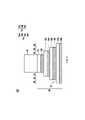
轉至圖31A、圖31B、圖31C及圖31D,亦可在導電線106及導電線108上形成多個接觸件。圖31A示出記憶體陣列200的透視圖;圖31B示出記憶體陣列200的俯視圖;且圖31C示出沿著圖31A的線31C-31C’的裝置及下伏基底的剖視圖;且圖31D示出沿著圖1A的參考橫截面B-B’的裝置的剖視圖。Turning to FIGS. 31A , 31B, 31C, and 31D, multiple contacts may also be formed on
如圖31A的透視圖所示,亦可分別製成至導電線106及導電線108的多個導電接觸件112及114。導電接觸件110、導電接觸件112及導電接觸件114可分別電性連接至導電線116A、導電線116B及導電線116C(統稱為導電線116),導電線116A、導電線116B及導電線116C將記憶體陣列200連接至半導體晶粒中的下伏/上覆電路系統(例如,控制電路系統)及/或訊號線、電源線及接地線。舉例而言,多個導電通孔118可延伸穿過金屬間介電層70,以將導電線116C電性連接至內連結構220的下伏電路系統及基底50上的主動裝置,如圖31C所示。可穿過金屬間介電層70形成其他導電通孔,以將導電線116A及導電線116B電性連接至內連結構220的下伏電路系統。在替代實施例中,除了內連結構220之外或代替內連結構220,可藉由形成於記憶體陣列200之上的內連結構來提供往來於記憶體陣列的佈線及/或電源線。因此,可完成記憶體陣列200。As shown in the perspective view of FIG. 31A, a plurality of
儘管圖2至圖31B的實施例示出導電線106及導電線108的特定圖案,但是其他配置亦是可能的。舉例而言,在該些實施例中,導電線106及導電線108具有交錯的圖案。在一些實施例中,位於陣列的同一列中的導電線106及導電線108均彼此對齊。Although the embodiments of FIGS. 2-31B show
圖32示出根據一些實施例的製造記憶體陣列200中的中間步驟的剖視圖。圖32中所示的結構與圖30中所示的結構相似,除了密封件140的突出至空氣隙132中的側壁具有實質上凸出形狀而不是實質上平的形狀。在一些情況下,在沈積期間形成密封材料134的一或多種前驅物相較於介電表面而更不可能黏附至金屬表面。舉例而言,相較於金屬間介電層70的氧化物材料,前驅物可能不太黏附至導電線72的金屬材料。此會導致密封材料134在導電線72上的緩慢或延遲的沈積,此會導致當在空氣隙132內形成密封材料134時使得密封材料134形成凸出側壁。一旦空氣隙132被密封材料134完全密封,則沒有其他前驅物可進入空氣隙132,並剩下密封材料134的凸出側壁。在一些情況下,如上所述,密封材料134在導電線72上的緩慢或延遲的沈積可限制密封材料134延伸至空氣隙132中的距離。藉由以此種方式限制或減小密封件140在空氣隙中的突出,可使空氣隙132被形成為具有相對較長的長度L5,此可使得導電線72之間的寄生電容減小。32 shows a cross-sectional view of an intermediate step in fabricating a
圖33示出根據一些實施例的製造記憶體陣列200中的中間步驟的剖視圖。圖33中所示的結構與圖30中所示的結構相似,除了密封件140形成在每一空氣隙132的兩端上。在其他實施例中,密封件140及/或接觸件110可以其他配置形成。舉例而言,密封件140可形成在導電線72的一端,但是接觸件110形成在該導電線72的兩端。作為另一實例,密封件140可形成在導電線72的一端,但是接觸件110形成在導電線72的相對端處。其他配置是可能的,且被認為處於本揭露的範圍內。33 shows a cross-sectional view of an intermediate step in fabricating a
圖34示出根據一些實施例的製造記憶體陣列200中的中間步驟的剖視圖。圖34中所示的結構與圖33中所示的結構相似,除了導電線72具有彎曲的形狀。在一些情況下,在移除犧牲層74以形成空氣隙132之後,導電線72可彎折(bow)、彎曲(bend)或下垂(sag)。導電線72可具有比圖34中所示的曲率更大或更小的曲率,及/或不同導電線72可具有不同的曲率。在一些實施例中,導電線72可透過處於約30微米與約100微米之間的範圍內的垂直距離來下垂,儘管其他距離是可能的。在一些實施例中,由於下垂,空氣隙132在其中心附近的高度可大於該空氣隙132在其端部附近的高度。舉例而言,多層堆疊58的最頂部空氣隙132的中心附近的高度H1可大於該最頂部空氣隙132的端部附近的高度H2。在其他實施例中,高度H1可與高度H2大致相同。在一些實施例中,空氣隙132在其中心附近的高度H3可較該空氣隙132在其端部附近的高度H4大、小或與所述高度H4大致相同。在一些實施例中,多層堆疊58的最頂部空氣隙132下方的空氣隙132中的一或多者可具有較最頂部空氣隙132的高度H1小的高度(例如,圖34中所示的高度H3或H5)。在其他實施例中,不同空氣隙132的高度可為相似的,或者第一空氣隙132的高度可大於其上方的第二空氣隙132的高度。在一些實施例中,多層堆疊58的最頂部空氣隙132可具有該多層堆疊58中的空氣隙132的最大高度(例如,圖34中的高度H1),及/或多層堆疊58的最底部空氣隙132可具有在該多層堆疊58中的空氣隙132的最小高度(例如,圖34中的高度H5)。多層堆疊58中的空氣隙132的高度可與此處闡述的其他組合相似或不同,且所有此種組合均被認為處於本揭露的範圍內。34 shows a cross-sectional view of an intermediate step in fabricating a
圖35A至圖35C示出根據一些實施例的具有不同形狀的電晶體204的平面圖。圖35A至圖35C各自示出與圖25B中的平面圖相似的平面圖的放大部分,除了介電材料102、記憶體膜90、氧化物半導體層92、導電線106、導電線108及介電材料98具有與圖25B中不同的形狀。圖35A至圖35C中所示的實施例可部分或全部併入至本文中闡述的其他實施例中。圖35A至圖35C中所示的結構是實例,且其他結構是可能的。35A-35C illustrate plan views of
在圖35A中,記憶體膜90、氧化物半導體層92、導電線106及導電線108被形成為具有圓的形狀,例如具有圓形、橢圓形或一般而言為圓的橫截面的形狀。在一些實施例中,可藉由在介電材料98中蝕刻出溝渠88(參見圖20A至圖20C)來形成圖35A中所示的結構,使得溝渠88具有圓的形狀。可藉由例如在用於圖案化溝渠88的光阻中圖案化出具有圓的形狀的開口來形成具有圓的形狀的溝渠88。記憶體膜90及沈積在溝渠88中的氧化物半導體層92(參見圖21至圖22)因此具有對應的圓形狀。在沈積介電材料102(參見圖23A至圖23C)之後,可在介電材料102中形成具有圓的形狀的溝渠120(參見圖24A至圖24C)。因此,沈積在溝渠120中的導電材料104形成具有相似圓的形狀的導電線106及導電線108。In FIG. 35A, the
在圖35B中,導電線106及導電線108被形成為具有圓的形狀,且記憶體膜90並未被形成為跨越介電材料98的側壁延伸。在一些實施例中,可藉由使用選擇性沈積製程將記憶體膜90沈積在溝渠88內(參見圖21)來形成圖35B中所示的結構。舉例而言,可選擇或控制沈積製程的前驅物,使得記憶體膜90選擇性地沈積在除介電材料98的表面以外的表面上。可選擇介電材料98的材料以增強或提供此沈積選擇性。在沈積氧化物半導體層92及介電材料102(參見圖22至圖23C)之後,可在介電材料102中形成具有圓的形狀的溝渠120(參見圖24A至圖24C)。因此,沈積在溝渠120中的導電材料104形成具有相似圓的形狀的導電線106及導電線108。在一些情況下,形成與圖35B中所示電晶體相似的電晶體204可增大導電線106及導電線108與氧化物半導體層92之間的接觸面積,此可減小導電線106及導電線108與氧化物半導體層92之間的接觸電阻。在一些情況下,以此種方式形成導電線106及導電線108可使接觸區域的側向範圍透過處於約5奈米至約15奈米的範圍內的距離來增大。In FIG. 35B ,
在圖35C中,記憶體膜90及氧化物半導體層92兩者均不被形成為跨越介電材料98的側壁延伸,且導電線106及導電線108被形成為具有部分圓的形狀且跨越介電材料98延伸。在一些實施例中,可藉由選擇性沈積氧化物半導體層92來形成圖35C中所示的結構。在一些情況下,形成與圖35C中所示電晶體相似的電晶體204可增大導電線106及導電線108與氧化物半導體層92之間的接觸面積,此可減小導電線106及導電線108與氧化物半導體層92之間的接觸電阻。在一些情況下,以此種方式形成導電線106及導電線108可使接觸面積的側向範圍透過處於約5奈米至約30奈米的範圍內的距離增大。In FIG. 35C, both the
各種實施例提供一種具有垂直堆疊的多個記憶胞的3D記憶體陣列。所述多個記憶胞各自包括具有記憶體膜、閘極介電材料及氧化物半導體通道區的電晶體。所述電晶體各自包括多個源極/汲極電極,所述多個源極/汲極電極亦是所述記憶體陣列中的多個源極線及多個位元線。所述電晶體更包括閘極電極,所述多個閘極電極亦是記憶體陣列中的多個字元線。介電材料設置於所述多個源極/汲極電極之間並將所述多個源極/汲極電極中的相鄰的多個源極/汲極電極隔離開。在一些實施例中,在所述多個字元線的垂直堆疊中的每一字元線之間形成犧牲層。移除所述犧牲層,進而在垂直相鄰的所述多個字元線之間形成多個空氣隙。由於空氣具有較許多其他介電材料(例如,氧化物、氮化物等)低的介電常數,因此使用所述多個空氣隙而不是介電材料將所述多個字元線隔開可減小不同字元線之間的寄生電容。藉由以此種方式減小寄生電容,可改善裝置的速度(例如,響應速度、切換速度等),且可減小寄生雜訊。此可改善裝置的操作,特別是當以相對高的頻率運作時。Various embodiments provide a 3D memory array with vertically stacked multiple memory cells. Each of the plurality of memory cells includes a transistor having a memory film, a gate dielectric material, and an oxide semiconductor channel region. The transistors each include a plurality of source/drain electrodes, which are also a plurality of source lines and a plurality of bit lines in the memory array. The transistor further includes a gate electrode, and the plurality of gate electrodes are also a plurality of word lines in the memory array. A dielectric material is disposed between the plurality of source/drain electrodes and isolates adjacent ones of the plurality of source/drain electrodes. In some embodiments, a sacrificial layer is formed between each word line in the vertical stack of the plurality of word lines. The sacrificial layer is removed to form a plurality of air gaps between the vertically adjacent word lines. Since air has a lower dielectric constant than many other dielectric materials (eg, oxides, nitrides, etc.), using the plurality of air gaps rather than a dielectric material to separate the plurality of wordlines can reduce the Small parasitic capacitance between different word lines. by this wayIn this way, parasitic capacitance can be reduced, the speed of the device (eg, response speed, switching speed, etc.) can be improved, and parasitic noise can be reduced. This can improve the operation of the device, especially when operating at relatively high frequencies.
根據一些實施例,一種記憶體裝置包括:半導體基底;第一電晶體,位於所述半導體基底之上,其中所述第一電晶體包括在所述半導體基底之上延伸的第一字元線;第二電晶體,位於所述半導體基底之上,其中所述第二電晶體包括在所述第一字元線之上延伸的第二字元線;第一空氣隙,在所述第一字元線與所述第二字元線之間延伸;記憶體膜,沿著所述第一字元線及所述第二字元線延伸,其中所述記憶體膜接觸所述第一字元線及所述第二字元線;通道層,沿著所述記憶體膜延伸;源極線,沿著所述通道層延伸,其中所述記憶體膜位於所述源極線與所述第一字元線之間;位元線,沿著所述通道層延伸,其中所述記憶體膜位於所述位元線與所述第一字元線之間;以及隔離區,位於所述源極線與所述位元線之間。在實施例中,所述第一空氣隙的至少一端由在所述第一字元線與所述第二字元線之間延伸的第一介電材料密封。在實施例中,所述記憶體裝置包括導電接觸件,所述導電接觸件延伸穿過所述第一介電材料以在實體上接觸所述第一字元線。在實施例中,所述記憶體裝置包括金屬間介電層(IMD),所述金屬間介電層位於所述第一字元線及所述第一介電材料之上且在實體上接觸所述第一字元線及所述第一介電材料。在實施例中,所述第一空氣隙具有第一長度且所述第二字元線具有第二長度,其中所述第一長度處於所述第二長度的5%至80%的範圍內。在實施例中,所述記憶體裝置包括第二介電材料,所述第二介電材料在所述第二字元線之上延伸且在實體上接觸所述第二字元線。在實施例中,所述記憶體裝置包括:第三電晶體,位於所述半導體基底之上,其中所述第三電晶體包括在所述第二字元線之上延伸的第三字元線;以及第二空氣隙,在所述第二字元線與所述第三字元線之間延伸。在實施例中,所述第二空氣隙的體積小於所述第一空氣隙的體積。According to some embodiments, a memory device includes: a semiconductor substrate; a first transistor over the semiconductor substrate, wherein the first transistor includes a first word line extending over the semiconductor substrate; a second transistor on the semiconductor substrate, wherein the second transistor includes a second word line extending over the first word line; a first air gap on the first word line extending between the element line and the second word line; a memory film extending along the first word line and the second word line, wherein the memory film contacts the first word element line and the second word line; a channel layer extending along the memory film; a source line extending along the channel layer, wherein the memory film is located between the source line and the first between a word line; a bit line extending along the channel layer, wherein the memory film is located between the bit line and the first word line; and an isolation region located at the source between the polar line and the bit line. In an embodiment, at least one end of the first air gap is sealed by a first dielectric material extending between the first word line and the second word line. In an embodiment, the memory device includes conductive contacts extending through the first dielectric material to physically contact the first word line. In an embodiment, the memory device includes an intermetal dielectric (IMD) layer overlying and physically contacting the first word line and the first dielectric material the first word line and the first dielectric material. In an embodiment, the first air gap has a first length and the second word line has a second lengthdegrees, wherein the first length is in the range of 5% to 80% of the second length. In an embodiment, the memory device includes a second dielectric material extending over and physically contacting the second word line. In an embodiment, the memory device includes: a third transistor over the semiconductor substrate, wherein the third transistor includes a third word line extending over the second word line ; and a second air gap extending between the second word line and the third word line. In an embodiment, the volume of the second air gap is smaller than the volume of the first air gap.
根據一些實施例,一種裝置包括:半導體基底;第一記憶胞,位於所述半導體基底之上,所述第一記憶胞包括第一電晶體,其中所述第一電晶體包括:第一閘極電極,包括第一字元線的一部分,其中所述第一閘極電極的底表面被第一空氣隙暴露出,其中所述第一閘極電極的頂表面被第二空氣隙暴露出;鐵電材料的第一部分,其中所述鐵電材料的所述第一部分位於所述第一閘極電極的側壁上;以及第一通道區,位於所述鐵電材料的所述第一部分的側壁上。所述裝置亦包括:源極線,其中所述源極線的第一部分為所述第一電晶體提供第一源極/汲極電極;位元線,其中所述位元線的第一部分為所述第一電晶體提供第二源極/汲極電極;以及第一介電材料,將所述源極線與所述位元線隔開。在實施例中,所述裝置包括第二記憶胞,所述第二記憶胞位於所述第一記憶胞之上,所述第二記憶胞包括第二電晶體,其中所述第二電晶體包括第二閘極電極,所述第二閘極電極包括第二字元線的一部分,其中所述第二閘極電極的底表面被所述第二空氣隙暴露出。在實施例中,所述第二閘極電極的頂表面被第二介電材料覆蓋。在實施例中,所述第一閘極電極的所述底表面包括第一端及第二端,其中所述底表面的位於所述第一端與所述第二端之間的一部分較所述第一端及所述第二端更接近所述半導體基底。在實施例中,所述第二空氣隙的高度大於所述第一空氣隙的高度。在實施例中,所述裝置包括第一密封件及第二密封件,所述第一密封件位於所述第一閘極電極的所述底表面上,所述第二密封件位於所述第一閘極電極的所述頂表面上,其中所述第一密封件及所述第二密封件是密封材料。在實施例中,所述源極線的橫截面及所述位元線的橫截面具有圓的形狀。According to some embodiments, an apparatus includes: a semiconductor substrate; a first memory cell overlying the semiconductor substrate, the first memory cell including a first transistor, wherein the first transistor includes: a first gate an electrode comprising a portion of a first word line, wherein a bottom surface of the first gate electrode is exposed by a first air gap, wherein a top surface of the first gate electrode is exposed by a second air gap; iron a first portion of electrical material, wherein the first portion of the ferroelectric material is located on the sidewall of the first gate electrode; and a first channel region is located on the sidewall of the first portion of the ferroelectric material. The device also includes: a source line, wherein a first portion of the source line provides a first source/drain electrode for the first transistor; a bit line, wherein the first portion of the bit line is The first transistor provides a second source/drain electrode; and a first dielectric material separating the source line from the bit line. In an embodiment, the device includes a second memory cell overlying the first memory cell, the second memory cell including a second transistor, wherein the second transistor includes a second gate electrode, the second gate electrode includes a second charactera portion of the line wherein the bottom surface of the second gate electrode is exposed by the second air gap. In an embodiment, the top surface of the second gate electrode is covered with a second dielectric material. In an embodiment, the bottom surface of the first gate electrode includes a first end and a second end, wherein a portion of the bottom surface located between the first end and the second end is relatively The first end and the second end are closer to the semiconductor substrate. In an embodiment, the height of the second air gap is greater than the height of the first air gap. In an embodiment, the device includes a first seal on the bottom surface of the first gate electrode and a second seal on the bottom surface of the first gate electrode. On the top surface of a gate electrode, wherein the first seal and the second seal are sealing materials. In an embodiment, the cross-section of the source line and the cross-section of the bit line have the shape of a circle.
根據一些實施例,一種方法包括:沈積具有導電材料與犧牲材料的多個交替層以形成多層堆疊,所述多層堆疊包括多個導電材料層及多個犧牲材料層;沿著所述多層堆疊的側壁沈積記憶體膜;在所述記憶體膜之上沈積氧化物半導體(OS)層;在所述多層堆疊之上形成金屬間介電層(IMD);在所述金屬間介電層中圖案化出多個溝渠,其中所述多個溝渠中的每一溝渠暴露出所述多個犧牲材料層中的相應的犧牲材料層;透過所述多個溝渠執行蝕刻製程以移除所述多個犧牲材料層,其中移除所述多個犧牲材料層會形成位於所述多個導電材料層中的多個導電材料層之間的多個空氣隙;以及在所述多個溝渠中沈積介電材料,其中所述介電材料將所述多個空氣隙密封。在實施例中,所述犧牲材料是矽。在實施例中,所述蝕刻製程包括執行乾式蝕刻製程且接著執行濕式蝕刻製程。在實施例中,沈積所述介電材料包括使用PECVD製程來沈積氧化物。在實施例中,所述方法包括形成通往所述多個導電材料層的多個接觸件,此包括在所述多個溝渠中沈積導電材料。According to some embodiments, a method includes: depositing a plurality of alternating layers of conductive material and sacrificial material to form a multi-layer stack, the multi-layer stack including a plurality of layers of conductive material and a plurality of sacrificial material layers; sidewall deposition of a memory film; deposition of an oxide semiconductor (OS) layer over the memory film; formation of an intermetal dielectric (IMD) over the multilayer stack; patterning in the IMD forming a plurality of trenches, wherein each trench of the plurality of trenches exposes a corresponding sacrificial material layer of the plurality of sacrificial material layers; performing an etching process through the plurality of trenches to remove the plurality of a sacrificial material layer, wherein removing the plurality of sacrificial material layers forms a plurality of air gaps between the plurality of conductive material layers of the plurality of conductive material layers; and depositing a dielectric in the plurality of trenches material, wherein the dielectric material seals the plurality of air gaps. In an embodiment, the sacrificial material issilicon. In an embodiment, the etching process includes performing a dry etching process followed by performing a wet etching process. In an embodiment, depositing the dielectric material includes depositing an oxide using a PECVD process. In an embodiment, the method includes forming a plurality of contacts to the plurality of layers of conductive material, which includes depositing a conductive material in the plurality of trenches.
以上概述了若干實施例的特徵,以使熟習此項技術者可更佳地理解本揭露的各個態樣。熟習此項技術者應理解,他們可容易地使用本揭露作為設計或修改其他製程及結構的基礎來施行與本文中所介紹的實施例相同的目的及/或達成與本文中所介紹的實施例相同的優點。熟習此項技術者亦應認識到,該些等效構造並不背離本揭露的精神及範圍,而且他們可在不背離本揭露的精神及範圍的條件下對本文作出各種改變、代替及變更。The foregoing outlines the features of several embodiments so that those skilled in the art may better understand the various aspects of the present disclosure. Those skilled in the art should appreciate that they may readily use the present disclosure as a basis for designing or modifying other processes and structures for carrying out the same purposes and/or for achieving the embodiments described herein Same advantages. Those skilled in the art should also realize that these equivalent constructions do not depart from the spirit and scope of the present disclosure, and that they can make various changes, substitutions and alterations herein without departing from the spirit and scope of the present disclosure.
72、106、108:導電線72, 106, 108: Conductive wire
74:絕緣層74: Insulation layer
90:記憶體膜90: Memory film
92:氧化物半導體層92: oxide semiconductor layer
98、102:介電材料98, 102: Dielectric materials
132:空氣隙/第一空氣隙/第二空氣隙132: air gap/first air gap/second air gap
140:密封件140: Seals
200:記憶體陣列200: memory array
202:記憶胞202: Memory Cell
204:電晶體204: Transistor
207:箭頭207: Arrow
B-B’、C-C’、D-D’:參考橫截面B-B', C-C', D-D': Reference cross section
Claims (10)
Translated fromChineseApplications Claiming Priority (4)
| Application Number | Priority Date | Filing Date | Title |
|---|---|---|---|
| US202063044588P | 2020-06-26 | 2020-06-26 | |
| US63/044,588 | 2020-06-26 | ||
| US17/159,830US11600520B2 (en) | 2020-06-26 | 2021-01-27 | Air gaps in memory array structures |
| US17/159,830 | 2021-01-27 |
Publications (2)
| Publication Number | Publication Date |
|---|---|
| TW202201739A TW202201739A (en) | 2022-01-01 |
| TWI763375Btrue TWI763375B (en) | 2022-05-01 |
Family
ID=78066095
Family Applications (1)
| Application Number | Title | Priority Date | Filing Date |
|---|---|---|---|
| TW110109273ATWI763375B (en) | 2020-06-26 | 2021-03-16 | Memory device and manufacturing method thereof |
Country Status (5)
| Country | Link |
|---|---|
| US (2) | US11600520B2 (en) |
| KR (1) | KR102638126B1 (en) |
| CN (1) | CN113517302B (en) |
| DE (1) | DE102021102547A1 (en) |
| TW (1) | TWI763375B (en) |
Families Citing this family (23)
| Publication number | Priority date | Publication date | Assignee | Title |
|---|---|---|---|---|
| KR102521580B1 (en)* | 2019-07-31 | 2023-04-12 | 삼성전자주식회사 | Semiconductor device |
| DE102020130975B4 (en) | 2020-05-28 | 2025-08-14 | Taiwan Semiconductor Manufacturing Co., Ltd. | FERROELECTRIC STORAGE DEVICE AND METHOD FOR FORMING THE SAME |
| US11910617B2 (en) | 2020-05-28 | 2024-02-20 | Taiwan Semiconductor Manufacturing Company, Ltd. | Ferroelectric memory device and method of forming the same |
| US11653500B2 (en) | 2020-06-25 | 2023-05-16 | Taiwan Semiconductor Manufacturing Co., Ltd. | Memory array contact structures |
| US11985825B2 (en) | 2020-06-25 | 2024-05-14 | Taiwan Semiconductor Manufacturing Co., Ltd. | 3D memory array contact structures |
| US11600520B2 (en) | 2020-06-26 | 2023-03-07 | Taiwan Semiconductor Manufacturing Co., Ltd. | Air gaps in memory array structures |
| US11532343B2 (en) | 2020-06-26 | 2022-12-20 | Taiwan Semiconductor Manufacturing Co., Ltd. | Memory array including dummy regions |
| US11495618B2 (en) | 2020-07-30 | 2022-11-08 | Taiwan Semiconductor Manufacturing Co., Ltd. | Three-dimensional memory device and method |
| KR102865678B1 (en)* | 2020-09-23 | 2025-09-29 | 삼성전자주식회사 | Semiconductor device and electronic system including the same |
| US11716856B2 (en)* | 2021-03-05 | 2023-08-01 | Taiwan Semiconductor Manufacturing Co., Ltd. | Three-dimensional memory device and method |
| US11657863B2 (en)* | 2021-06-17 | 2023-05-23 | Taiwan Semiconductor Manufacturing Co., Ltd. | Memory array test structure and method of forming the same |
| US12408347B2 (en)* | 2021-07-21 | 2025-09-02 | Taiwan Semiconductor Manufacturing Company, Ltd. | Method for forming a 3-D semiconductor memory structure comprising horizontal and vertical conductive lines |
| US12402319B2 (en) | 2021-09-14 | 2025-08-26 | Sunrise Memory Corporation | Three-dimensional memory string array of thin-film ferroelectric transistors formed with an oxide semiconductor channel |
| US20230230921A1 (en)* | 2022-01-18 | 2023-07-20 | Taiwan Semiconductor Manufacturing Company, Ltd. | Semiconductor memory device and method for manufacturing the same |
| US20230262988A1 (en)* | 2022-02-14 | 2023-08-17 | Sunrise Memory Corporation | Memory structure including three-dimensional nor memory strings of junctionless ferroelectric memory transistors and method of fabrication |
| TWI809855B (en)* | 2022-05-05 | 2023-07-21 | 旺宏電子股份有限公司 | Memory device, semiconductor device, and method of fabricating the same |
| US12382635B2 (en)* | 2022-06-21 | 2025-08-05 | Macronix International Co., Ltd. | 3D flash memory device and method of manufacturing the same |
| US12328868B2 (en)* | 2022-07-22 | 2025-06-10 | Nanya Technology Corporation | Memory structure including low dielectric constant capping layer |
| CN116761423B (en)* | 2023-02-08 | 2024-03-01 | 北京超弦存储器研究院 | 3D stacked semiconductor device, manufacturing method thereof, 3D memory and electronic equipment |
| CN116367539B (en)* | 2023-04-20 | 2024-01-19 | 北京超弦存储器研究院 | Semiconductor device, memory, manufacturing method of memory and electronic equipment |
| CN118942494A (en)* | 2023-05-12 | 2024-11-12 | 北京超弦存储器研究院 | Memory and preparation method thereof, and electronic device |
| US12087669B1 (en)* | 2023-08-14 | 2024-09-10 | Samsung Electronics Co., Ltd. | Integrated circuit devices including discharging path and methods of forming the same |
| CN119545781A (en)* | 2023-08-31 | 2025-02-28 | 北京超弦存储器研究院 | Three-dimensional memory and manufacturing method thereof, and electronic device |
Citations (3)
| Publication number | Priority date | Publication date | Assignee | Title |
|---|---|---|---|---|
| TWI643317B (en)* | 2017-12-01 | 2018-12-01 | 旺宏電子股份有限公司 | Memory device and method for fabricating the same |
| TWI643318B (en)* | 2017-12-01 | 2018-12-01 | 旺宏電子股份有限公司 | Memory device and method for operating the same |
| US20200194451A1 (en)* | 2018-12-12 | 2020-06-18 | Samsung Electronics Co., Ltd. | Vertical semiconductor devices |
Family Cites Families (126)
| Publication number | Priority date | Publication date | Assignee | Title |
|---|---|---|---|---|
| US7256098B2 (en) | 2005-04-11 | 2007-08-14 | Infineon Technologies Ag | Method of manufacturing a memory device |
| EP1770788A3 (en) | 2005-09-29 | 2011-09-21 | Semiconductor Energy Laboratory Co., Ltd. | Semiconductor device having oxide semiconductor layer and manufacturing method thereof |
| JP2007281199A (en) | 2006-04-06 | 2007-10-25 | Toshiba Corp | Semiconductor device |
| JP2008277543A (en) | 2007-04-27 | 2008-11-13 | Toshiba Corp | Nonvolatile semiconductor memory device |
| JP2009016400A (en) | 2007-06-29 | 2009-01-22 | Toshiba Corp | LAMINATED WIRING STRUCTURE AND METHOD FOR MANUFACTURING SAME |
| JP5305980B2 (en) | 2009-02-25 | 2013-10-02 | 株式会社東芝 | Nonvolatile semiconductor memory device and manufacturing method thereof |
| JP2011023687A (en) | 2009-07-21 | 2011-02-03 | Toshiba Corp | Nonvolatile semiconductor memory device |
| JP2011060958A (en) | 2009-09-09 | 2011-03-24 | Toshiba Corp | Semiconductor device, and method of manufacturing the same |
| IN2012DN06399A (en) | 2010-02-07 | 2015-10-02 | Zeno Semiconductor Inc | |
| KR101102548B1 (en) | 2010-04-30 | 2012-01-04 | 한양대학교 산학협력단 | Nonvolatile Memory Device and Manufacturing Method Thereof |
| KR101660432B1 (en) | 2010-06-07 | 2016-09-27 | 삼성전자 주식회사 | Semiconductor memory device having vertical structure |
| KR20130066950A (en)* | 2011-12-13 | 2013-06-21 | 에스케이하이닉스 주식회사 | Three dimension non-volatile memory device, memory system comprising the same and method of manufacturing the same |
| US8847302B2 (en)* | 2012-04-10 | 2014-09-30 | Sandisk Technologies Inc. | Vertical NAND device with low capacitance and silicided word lines |
| TWI488265B (en) | 2012-07-11 | 2015-06-11 | Powerchip Technology Corp | Stereo vertical memory manufacturing method |
| KR20140024632A (en) | 2012-08-20 | 2014-03-03 | 삼성전자주식회사 | Three dimensional semiconductor memory device method for manufacturing the same |
| US9698153B2 (en) | 2013-03-12 | 2017-07-04 | Sandisk Technologies Llc | Vertical NAND and method of making thereof using sequential stack etching and self-aligned landing pad |
| US9184175B2 (en) | 2013-03-15 | 2015-11-10 | Micron Technology, Inc. | Floating gate memory cells in vertical memory |
| CN104112748B (en) | 2013-04-19 | 2016-12-28 | 中国科学院微电子研究所 | Memory device, method of manufacturing the same, and method of accessing the same |
| US9240420B2 (en) | 2013-09-06 | 2016-01-19 | Sandisk Technologies Inc. | 3D non-volatile storage with wide band gap transistor decoder |
| WO2015102746A2 (en) | 2013-11-04 | 2015-07-09 | Massachusetts Institute Of Technology | Electronics including graphene-based hybrid structures |
| KR102161781B1 (en) | 2014-02-03 | 2020-10-05 | 삼성전자주식회사 | Vertical memory devices |
| JP2015149413A (en) | 2014-02-06 | 2015-08-20 | 株式会社東芝 | Semiconductor memory device and manufacturing method thereof |
| KR20150118648A (en) | 2014-04-14 | 2015-10-23 | 삼성전자주식회사 | Nonvolatile memory device |
| US9015561B1 (en) | 2014-06-11 | 2015-04-21 | Sandisk Technologies Inc. | Adaptive redundancy in three dimensional memory |
| US9455263B2 (en) | 2014-06-27 | 2016-09-27 | Sandisk Technologies Llc | Three dimensional NAND device with channel contacting conductive source line and method of making thereof |
| US9263143B2 (en) | 2014-07-14 | 2016-02-16 | Macronix International Co., Ltd. | Three dimensional memory device and data erase method thereof |
| US9576975B2 (en)* | 2014-08-26 | 2017-02-21 | Sandisk Technologies Llc | Monolithic three-dimensional NAND strings and methods of fabrication thereof |
| US10014317B2 (en) | 2014-09-23 | 2018-07-03 | Haibing Peng | Three-dimensional non-volatile NOR-type flash memory |
| TW201624708A (en) | 2014-11-21 | 2016-07-01 | 半導體能源研究所股份有限公司 | Semiconductor device and memory device |
| US9355727B1 (en) | 2014-12-09 | 2016-05-31 | Sandisk Technologies Inc. | Three-dimensional memory structure having a back gate electrode |
| EP3231012B1 (en) | 2014-12-09 | 2023-09-20 | SanDisk Technologies LLC | Three-dimensional memory structure having a back gate electrode |
| EP3038141B1 (en) | 2014-12-23 | 2019-08-28 | IMEC vzw | Method of reading a memory cell of a vertical ferroelectric memory device |
| US9818848B2 (en) | 2015-04-29 | 2017-11-14 | Yale University | Three-dimensional ferroelectric FET-based structures |
| CN108401468A (en) | 2015-09-21 | 2018-08-14 | 莫诺利特斯3D有限公司 | 3D semiconductor devices and structures |
| US20190148286A1 (en) | 2015-09-21 | 2019-05-16 | Monolithic 3D Inc. | Multi-level semiconductor device and structure with memory |
| US11120884B2 (en) | 2015-09-30 | 2021-09-14 | Sunrise Memory Corporation | Implementing logic function and generating analog signals using NOR memory strings |
| US9842651B2 (en) | 2015-11-25 | 2017-12-12 | Sunrise Memory Corporation | Three-dimensional vertical NOR flash thin film transistor strings |
| KR102435524B1 (en) | 2015-10-21 | 2022-08-23 | 삼성전자주식회사 | Semiconductor memory device |
| US9502265B1 (en) | 2015-11-04 | 2016-11-22 | Taiwan Semiconductor Manufacturing Company, Ltd. | Vertical gate all around (VGAA) transistors and methods of forming the same |
| EP3381036B1 (en)* | 2015-11-25 | 2021-07-21 | Sunrise Memory Corporation | Three-dimensional vertical nor flash thin film transistor strings |
| JP2017103328A (en)* | 2015-12-01 | 2017-06-08 | 株式会社東芝 | Semiconductor device and manufacturing method of the same |
| US10128264B2 (en) | 2016-01-21 | 2018-11-13 | SK Hynix Inc. | Semiconductor device |
| KR102550575B1 (en) | 2016-01-26 | 2023-07-04 | 에스케이하이닉스 주식회사 | Semiconductor device and manufacturing method thereof |
| US9853047B2 (en) | 2016-01-26 | 2017-12-26 | SK Hynix Inc. | Semiconductor device and method of manufacturing the same |
| KR102594494B1 (en) | 2016-02-17 | 2023-10-27 | 에스케이하이닉스 주식회사 | Semiconductor device and manufacturing method thereof |
| SG10201701689UA (en) | 2016-03-18 | 2017-10-30 | Semiconductor Energy Lab | Semiconductor device, semiconductor wafer, and electronic device |
| KR102789289B1 (en) | 2016-04-18 | 2025-04-01 | 삼성전자주식회사 | Semiconductor memory device and semiconductor device |
| US9601497B1 (en) | 2016-04-28 | 2017-03-21 | Taiwan Semiconductor Manufacturing Co., Ltd. | Static random access memory and method of manufacturing the same |
| US9997631B2 (en) | 2016-06-03 | 2018-06-12 | Taiwan Semiconductor Manufacturing Company | Methods for reducing contact resistance in semiconductors manufacturing process |
| KR102626193B1 (en) | 2016-08-26 | 2024-01-18 | 선라이즈 메모리 코포레이션 | Capacitive-coupled non-volatile thin-film transistor strings in three dimensional arrays |
| US20180083018A1 (en) | 2016-09-19 | 2018-03-22 | Toshiba Memory Corporation | Semiconductor memory device and method of manufacturing the same |
| DE102017113967A1 (en) | 2016-09-26 | 2018-03-29 | Sandisk Technologies Llc | ADAPTIVE OPERATION OF 3-D MEMORY |
| CN106158877B (en) | 2016-09-30 | 2019-04-02 | 中国科学院微电子研究所 | Memory device, method of manufacturing the same, and electronic apparatus including the same |
| KR102653527B1 (en) | 2016-11-09 | 2024-04-01 | 에스케이하이닉스 주식회사 | Nonvolatile Memory Device and Method of Manufacturing the same |
| US12114494B2 (en) | 2017-02-04 | 2024-10-08 | Monolithic 3D Inc. | 3D memory semiconductor device and structure |
| EP3577689A4 (en) | 2017-02-04 | 2021-06-02 | Monolithic 3D Inc. | THREE-DIMENSIONAL SEMICONDUCTOR DEVICE AND STRUCTURE |
| KR102768958B1 (en) | 2017-03-08 | 2025-02-14 | 양쯔 메모리 테크놀로지스 씨오., 엘티디. | Through array contact structure of three-dimensional memory device |
| US10312239B2 (en) | 2017-03-16 | 2019-06-04 | Toshiba Memory Corporation | Semiconductor memory including semiconductor oxie |
| US20180315794A1 (en) | 2017-04-26 | 2018-11-01 | Sandisk Technologies Llc | Methods and apparatus for three-dimensional nonvolatile memory |
| US10043819B1 (en) | 2017-05-17 | 2018-08-07 | Macronix International Co., Ltd. | Method for manufacturing 3D NAND memory using gate replacement, and resulting structures |
| KR101933307B1 (en) | 2017-05-17 | 2019-03-15 | 연세대학교 산학협력단 | 3 dimensional non-volatile memory device and method of fabricating the same |
| KR20180131118A (en) | 2017-05-31 | 2018-12-10 | 에스케이하이닉스 주식회사 | semiconductor device having ferroelectric layer and method of fabricating the same |
| US11011529B2 (en) | 2017-06-29 | 2021-05-18 | Micron Technology, Inc. | Memory arrays comprising vertically-alternating tiers of insulative material and memory cells and methods of forming a memory array comprising memory cells individually comprising a transistor and a capacitor |
| US10665604B2 (en) | 2017-07-21 | 2020-05-26 | Semiconductor Energy Laboratory Co., Ltd. | Semiconductor device, semiconductor wafer, memory device, and electronic device |
| US10566519B2 (en) | 2017-08-18 | 2020-02-18 | Taiwan Semiconductor Manufacturing Co., Ltd. | Method for forming a flat bottom electrode via (BEVA) top surface for memory |
| JP6563988B2 (en) | 2017-08-24 | 2019-08-21 | ウィンボンド エレクトロニクス コーポレーション | Nonvolatile semiconductor memory device |
| US10346088B2 (en) | 2017-09-29 | 2019-07-09 | Intel Corporation | Method and apparatus for per-deck erase verify and dynamic inhibit in 3d NAND |
| CN109698162A (en) | 2017-10-20 | 2019-04-30 | 萨摩亚商费洛储存科技股份有限公司 | Three-dimensional memory element and method of manufacturing the same |
| US10777566B2 (en) | 2017-11-10 | 2020-09-15 | Macronix International Co., Ltd. | 3D array arranged for memory and in-memory sum-of-products operations |
| KR102565002B1 (en) | 2017-11-21 | 2023-08-08 | 삼성전자주식회사 | Three dimensional semiconductor memory device |
| WO2019125352A1 (en) | 2017-12-18 | 2019-06-27 | Intel Corporation | Three-dimensional integrated circuit memory cell having a ferroelectric field effect transistor with a floating gate |
| KR102626137B1 (en) | 2018-02-02 | 2024-01-18 | 선라이즈 메모리 코포레이션 | Three-dimensional vertical nor flash thin-film transistor strings |
| US10256247B1 (en) | 2018-02-08 | 2019-04-09 | Sandisk Technologies Llc | Three-dimensional memory device with silicided word lines, air gap layers and discrete charge storage elements, and method of making thereof |
| JP2019164868A (en) | 2018-03-20 | 2019-09-26 | 東芝メモリ株式会社 | Semiconductor storage device |
| US20190312050A1 (en) | 2018-04-10 | 2019-10-10 | Macronix International Co., Ltd. | String select line gate oxide method for 3d vertical channel nand memory |
| CN112768453B (en) | 2018-04-19 | 2024-04-26 | 长江存储科技有限责任公司 | Memory device and method of forming the same |
| US11362140B2 (en)* | 2018-06-29 | 2022-06-14 | Intel Corporation | Word line with air-gap for non-volatile memories |
| CN110707006B (en) | 2018-07-09 | 2023-10-17 | 日升存储公司 | In situ preparation method of antimony doped silicon and silicon germanium film |
| US10664746B2 (en) | 2018-07-17 | 2020-05-26 | Macronix International Co., Ltd. | Neural network system |
| US10784278B2 (en) | 2018-07-30 | 2020-09-22 | Taiwan Semiconductor Manufacturing Co., Ltd. | Memory device and manufacturing method thereof |
| US10741576B2 (en) | 2018-08-20 | 2020-08-11 | Sandisk Technologies Llc | Three-dimensional memory device containing drain-select-level air gap and methods of making the same |
| US11380709B2 (en)* | 2018-09-04 | 2022-07-05 | Sandisk Technologies Llc | Three dimensional ferroelectric memory |
| JP2020043119A (en) | 2018-09-06 | 2020-03-19 | キオクシア株式会社 | Semiconductor device |
| US10629608B2 (en) | 2018-09-26 | 2020-04-21 | Macronix International Co., Ltd. | 3D vertical channel tri-gate NAND memory with tilted hemi-cylindrical structure |
| US10651182B2 (en) | 2018-09-28 | 2020-05-12 | Intel Corporation | Three-dimensional ferroelectric NOR-type memory |
| EP3857608A4 (en)* | 2018-10-09 | 2022-09-21 | Micron Technology, Inc. | METHOD OF MAKING A DEVICE, RELATED DEVICES AND ELECTRONIC SYSTEMS |
| US10685971B2 (en)* | 2018-10-15 | 2020-06-16 | Macronix International Co., Ltd. | Three dimensional memory device and method for fabricating the same |
| TWI848993B (en) | 2018-10-26 | 2024-07-21 | 美商蘭姆研究公司 | Self-aligned vertical integration of three-terminal memory devices |
| EP3891780A4 (en) | 2018-12-07 | 2022-12-21 | Sunrise Memory Corporation | METHOD OF FABRICATION OF MULTILAYER VERTICAL NOR STORAGE STRING ARRAYS |
| KR102783249B1 (en) | 2018-12-10 | 2025-03-19 | 삼성전자주식회사 | Vertical memory devices |
| KR102658194B1 (en) | 2018-12-21 | 2024-04-18 | 삼성전자주식회사 | Semiconductor device |
| US10923502B2 (en) | 2019-01-16 | 2021-02-16 | Sandisk Technologies Llc | Three-dimensional ferroelectric memory devices including a backside gate electrode and methods of making same |
| TWI692038B (en) | 2019-01-25 | 2020-04-21 | 旺宏電子股份有限公司 | Three-dimensional stacked semiconductor device and method of manufacturing the same |
| TWI681548B (en) | 2019-02-12 | 2020-01-01 | 旺宏電子股份有限公司 | Three dimensional memory device and method for fabricating the same |
| JP2020150199A (en) | 2019-03-15 | 2020-09-17 | キオクシア株式会社 | Semiconductor storage device |
| JP2020155543A (en) | 2019-03-19 | 2020-09-24 | キオクシア株式会社 | Semiconductor storage device |
| US11069697B1 (en) | 2019-04-08 | 2021-07-20 | Monolithic 3D Inc. | 3D memory semiconductor devices and structures |
| US10910393B2 (en) | 2019-04-25 | 2021-02-02 | Macronix International Co., Ltd. | 3D NOR memory having vertical source and drain structures |
| US11069598B2 (en) | 2019-06-18 | 2021-07-20 | Micron Technology, Inc. | Memory arrays and methods used in forming a memory array and conductive through-array-vias (TAVs) |
| US10868042B1 (en) | 2019-06-28 | 2020-12-15 | Sandisk Technologies Llc | Ferroelectric memory device containing word lines and pass gates and method of forming the same |
| CN110520985B (en) | 2019-07-16 | 2020-08-25 | 长江存储科技有限责任公司 | Interconnect structure of three-dimensional memory device |
| KR102689479B1 (en) | 2019-08-01 | 2024-07-26 | 삼성전자주식회사 | Nonvolatile memory device and method for fabricating the same |
| US11239254B2 (en) | 2019-08-02 | 2022-02-01 | Sandisk Technologies Llc | Three-dimensional memory device containing epitaxial ferroelectric memory elements and methods for forming the same |
| KR102814246B1 (en) | 2019-08-26 | 2025-05-30 | 삼성전자주식회사 | Nonvolatile memory device, storage device, and operating method of nonvolatile memory device |
| US11211395B2 (en)* | 2019-08-30 | 2021-12-28 | Macronix International Co., Ltd. | 3D memory array having select lines |
| KR102711222B1 (en) | 2019-09-04 | 2024-09-27 | 삼성전자주식회사 | Vertical non-volatile memory devices and methods of programming in the same |
| US11398496B2 (en)* | 2020-04-27 | 2022-07-26 | Sandisk Technologies Llc | Three-dimensional memory device employing thinned insulating layers and methods for forming the same |
| US11171157B1 (en) | 2020-05-05 | 2021-11-09 | Taiwan Semiconductor Manufacturing Company, Ltd. | Method for forming a MFMIS memory device |
| US11335671B2 (en)* | 2020-05-28 | 2022-05-17 | Sandisk Technologies Llc | Stacked die assembly including double-sided inter-die bonding connections and methods of forming the same |
| US11574929B2 (en) | 2020-05-28 | 2023-02-07 | Taiwan Semiconductor Manufacturing Company, Ltd. | 3D ferroelectric memory |
| US11839080B2 (en) | 2020-05-28 | 2023-12-05 | Taiwan Semiconductor Manufacturing Company, Ltd. | 3D memory with graphite conductive strips |
| US11532640B2 (en) | 2020-05-29 | 2022-12-20 | Taiwan Semiconductor Manufacturing Co., Ltd. | Method for manufacturing a three-dimensional memory |
| US11695073B2 (en) | 2020-05-29 | 2023-07-04 | Taiwan Semiconductor Manufacturing Co., Ltd. | Memory array gate structures |
| US11404091B2 (en) | 2020-06-19 | 2022-08-02 | Taiwan Semiconductor Manufacturing Co., Ltd. | Memory array word line routing |
| WO2021261744A1 (en) | 2020-06-23 | 2021-12-30 | 한양대학교 산학협력단 | Three-dimensional flash memory comprising back gate |
| US11985825B2 (en) | 2020-06-25 | 2024-05-14 | Taiwan Semiconductor Manufacturing Co., Ltd. | 3D memory array contact structures |
| US11653500B2 (en) | 2020-06-25 | 2023-05-16 | Taiwan Semiconductor Manufacturing Co., Ltd. | Memory array contact structures |
| US11532343B2 (en) | 2020-06-26 | 2022-12-20 | Taiwan Semiconductor Manufacturing Co., Ltd. | Memory array including dummy regions |
| US11600520B2 (en) | 2020-06-26 | 2023-03-07 | Taiwan Semiconductor Manufacturing Co., Ltd. | Air gaps in memory array structures |
| US11444069B2 (en) | 2020-06-29 | 2022-09-13 | Taiwan Semiconductor Manufacturing Co., Ltd. | 3D semiconductor package including memory array |
| US11729987B2 (en) | 2020-06-30 | 2023-08-15 | Taiwan Semiconductor Manufacturing Company, Ltd. | Memory array source/drain electrode structures |
| US11640974B2 (en) | 2020-06-30 | 2023-05-02 | Taiwan Semiconductor Manufacturing Co., Ltd. | Memory array isolation structures |
| US11569165B2 (en) | 2020-07-29 | 2023-01-31 | Taiwan Semiconductor Manufacturing Company, Ltd. | Memory cell array, semiconductor device including the same, and manufacturing method thereof |
| US11527553B2 (en) | 2020-07-30 | 2022-12-13 | Taiwan Semiconductor Manufacturing Co., Ltd. | Three-dimensional memory device and method |
| US11495618B2 (en) | 2020-07-30 | 2022-11-08 | Taiwan Semiconductor Manufacturing Co., Ltd. | Three-dimensional memory device and method |
| US11423966B2 (en) | 2020-07-30 | 2022-08-23 | Taiwan Semiconductor Manufacturing Co., Ltd. | Memory array staircase structure |
- 2021
- 2021-01-27USUS17/159,830patent/US11600520B2/enactiveActive
- 2021-02-04DEDE102021102547.8Apatent/DE102021102547A1/enactivePending
- 2021-03-16TWTW110109273Apatent/TWI763375B/enactive
- 2021-03-30KRKR1020210041326Apatent/KR102638126B1/enactiveActive
- 2021-06-25CNCN202110708543.9Apatent/CN113517302B/enactiveActive
- 2023
- 2023-03-06USUS18/178,773patent/US12087621B2/enactiveActive
Patent Citations (4)
| Publication number | Priority date | Publication date | Assignee | Title |
|---|---|---|---|---|
| TWI643317B (en)* | 2017-12-01 | 2018-12-01 | 旺宏電子股份有限公司 | Memory device and method for fabricating the same |
| TWI643318B (en)* | 2017-12-01 | 2018-12-01 | 旺宏電子股份有限公司 | Memory device and method for operating the same |
| TW201926642A (en)* | 2017-12-01 | 2019-07-01 | 旺宏電子股份有限公司 | Memory device and method for fabricating the same |
| US20200194451A1 (en)* | 2018-12-12 | 2020-06-18 | Samsung Electronics Co., Ltd. | Vertical semiconductor devices |
Also Published As
| Publication number | Publication date |
|---|---|
| CN113517302A (en) | 2021-10-19 |
| CN113517302B (en) | 2024-12-27 |
| US20210407845A1 (en) | 2021-12-30 |
| DE102021102547A1 (en) | 2021-12-30 |
| US12087621B2 (en) | 2024-09-10 |
| KR102638126B1 (en) | 2024-02-16 |
| US11600520B2 (en) | 2023-03-07 |
| US20230215761A1 (en) | 2023-07-06 |
| KR20220000807A (en) | 2022-01-04 |
| TW202201739A (en) | 2022-01-01 |
Similar Documents
| Publication | Publication Date | Title |
|---|---|---|
| TWI763375B (en) | Memory device and manufacturing method thereof | |
| CN113675215B (en) | Memory array, memory device and forming method thereof | |
| TWI773164B (en) | Memory cell, semiconductor device and method of manufacturing semiconductor device | |
| CN113517301B (en) | Memory array device and method of forming the same | |
| TWI797568B (en) | Memory cell, semiconductor device and method of fabricating the same | |
| CN113745238B (en) | Three-dimensional storage device and method | |
| KR102611769B1 (en) | Memory array and methods of forming same | |
| TWI807270B (en) | Memory cell, semiconductor device, and method of forming semiconductor device | |
| US12167606B2 (en) | Memory device and method of forming thereof | |
| US20240260276A1 (en) | Air Gaps In Memory Array Structures | |
| TW202236621A (en) | Three-dimensional memory device and manufacturing method thereof | |
| US20240404875A1 (en) | Air gaps in memory array structures |