TWI762274B - System and method for adjusting circuit parameter and host system - Google Patents
System and method for adjusting circuit parameter and host systemDownload PDFInfo
- Publication number
- TWI762274B TWI762274BTW110113876ATW110113876ATWI762274BTW I762274 BTWI762274 BTW I762274BTW 110113876 ATW110113876 ATW 110113876ATW 110113876 ATW110113876 ATW 110113876ATW I762274 BTWI762274 BTW I762274B
- Authority
- TW
- Taiwan
- Prior art keywords
- circuit
- storage device
- memory storage
- signal
- relay
- Prior art date
Links
- 238000000034methodMethods0.000titleclaimsabstractdescription28
- 230000005055memory storageEffects0.000claimsabstractdescription126
- 238000012545processingMethods0.000claimsabstractdescription68
- 238000012360testing methodMethods0.000claimsdescription53
- 238000011084recoveryMethods0.000claimsdescription8
- 230000005540biological transmissionEffects0.000claimsdescription6
- 238000010586diagramMethods0.000description14
- 230000008054signal transmissionEffects0.000description5
- 238000005516engineering processMethods0.000description3
- 230000004044responseEffects0.000description3
- 238000001514detection methodMethods0.000description2
- 230000008859changeEffects0.000description1
- 230000008878couplingEffects0.000description1
- 238000010168coupling processMethods0.000description1
- 238000005859coupling reactionMethods0.000description1
- 238000011156evaluationMethods0.000description1
- 238000009434installationMethods0.000description1
- 238000012986modificationMethods0.000description1
- 230000004048modificationEffects0.000description1
- 230000002093peripheral effectEffects0.000description1
- 238000007781pre-processingMethods0.000description1
- 230000008569processEffects0.000description1
- 239000007787solidSubstances0.000description1
Images


Landscapes
- Optical Communication System (AREA)
- Signal Processing For Digital Recording And Reproducing (AREA)
- Transceivers (AREA)
Abstract
Description
Translated fromChinese本發明是有關於一種電路參數調整技術,且特別是有關於一種電路參數調整系統、方法及主機系統。The present invention relates to a circuit parameter adjustment technology, and in particular, to a circuit parameter adjustment system, method and host system.
訊號中繼器(re-driver)一般可用以延長訊號的傳輸距離。但是,在不同的使用環境及/或不同的配置條件下,訊號中繼器所預設使用的電路參數可能導致訊號中繼器對訊號的調變效率不佳。Signal repeaters (re-drivers) are generally used to extend the transmission distance of signals. However, under different usage environments and/or different configuration conditions, the preset circuit parameters of the signal repeater may result in poor signal modulation efficiency by the signal repeater.
本發明提供一種電路參數調整系統、方法及主機系統,可提高對於中繼電路使用的電路參數的調整效率。The present invention provides a circuit parameter adjustment system, method and host system, which can improve the adjustment efficiency of circuit parameters used in relay circuits.
本發明的範例實施例提供一種電路參數調整系統,其包括處理電路、中繼電路及記憶體儲存裝置。所述中繼電路耦接至所述處理電路。所述記憶體儲存裝置耦接至所述中繼電路。所述處理電路用以經由所述中繼電路傳送指令至所述記憶體儲存裝置。所述指令用以指示所述記憶體儲存裝置提供訊號品質資訊。所述處理電路更用以從所述記憶體儲存裝置接收所述訊號品質資訊。所述處理電路更用以根據所述訊號品質資訊調整所述中繼電路的電路參數。An exemplary embodiment of the present invention provides a circuit parameter adjustment system, which includes a processing circuit, a relay circuit, and a memory storage device. The relay circuit is coupled to the processing circuit. The memory storage device is coupled to the relay circuit. The processing circuit is used for transmitting an instruction to the memory storage device via the relay circuit. The command is used to instruct the memory storage device to provide signal quality information. The processing circuit is further configured to receive the signal quality information from the memory storage device. The processing circuit is further configured to adjust circuit parameters of the relay circuit according to the signal quality information.
在本發明的一範例實施例中,所述中繼電路用以調變在所述處理電路與所述記憶體儲存裝置之間傳遞的訊號,以延長所述訊號的傳輸距離。In an exemplary embodiment of the present invention, the relay circuit is used to modulate the signal transmitted between the processing circuit and the memory storage device, so as to extend the transmission distance of the signal.
在本發明的一範例實施例中,所述中繼電路包括發送端電路,且經調整的所述電路參數為所述發送端電路的至少一設定參數。In an exemplary embodiment of the present invention, the relay circuit includes a transmitter circuit, and the adjusted circuit parameter is at least one setting parameter of the transmitter circuit.
本發明的範例實施例另提供一種電路參數調整方法,其包括:經由中繼電路傳送指令至記憶體儲存裝置,其中所述指令用以指示所述記憶體儲存裝置提供訊號品質資訊;從所述記憶體儲存裝置接收所述訊號品質資訊;以及根據所述訊號品質資訊調整所述中繼電路的電路參數。An exemplary embodiment of the present invention further provides a circuit parameter adjustment method, which includes: sending an instruction to a memory storage device via a relay circuit, wherein the instruction is used to instruct the memory storage device to provide signal quality information; The memory storage device receives the signal quality information; and adjusts circuit parameters of the relay circuit according to the signal quality information.
在本發明的一範例實施例中,所述的電路參數調整方法更包括:經由所述中繼電路調變在處理電路與所述記憶體儲存裝置之間傳遞的訊號,以延長所述訊號的傳輸距離。In an exemplary embodiment of the present invention, the circuit parameter adjustment method further includes: modulating a signal transmitted between the processing circuit and the memory storage device via the relay circuit to extend the signal transmission distance.
在本發明的一範例實施例中,所述訊號品質資訊反映所述記憶體儲存裝置經由所述中繼電路接收到的測試訊號的訊號品質。In an exemplary embodiment of the present invention, the signal quality information reflects the signal quality of the test signal received by the memory storage device via the relay circuit.
在本發明的一範例實施例中,所述訊號品質資訊反映所述記憶體儲存裝置經由所述中繼電路接收到的所述測試訊號的訊號恢復狀態、訊號眼寬狀態、訊號眼高狀態及訊號邊緣狀態的至少其中之一。In an exemplary embodiment of the present invention, the signal quality information reflects a signal recovery state, a signal eye width state, and a signal eye height state of the test signal received by the memory storage device via the relay circuit and at least one of the signal edge states.
在本發明的一範例實施例中,經調整的所述電路參數用以提高所述中繼電路的運作效能。In an exemplary embodiment of the present invention, the adjusted circuit parameters are used to improve the operation performance of the relay circuit.
在本發明的一範例實施例中,所述處理電路與所述中繼電路設置於同一主機板上。In an exemplary embodiment of the present invention, the processing circuit and the relay circuit are disposed on the same motherboard.
在本發明的一範例實施例中,所述中繼電路包括發送端電路,且根據所述訊號品質資訊調整所述中繼電路的所述電路參數的步驟包括:根據所述訊號品質資訊調整所述發送端電路的至少一設定參數。In an exemplary embodiment of the present invention, the relay circuit includes a transmitter circuit, and the step of adjusting the circuit parameters of the relay circuit according to the signal quality information includes: according to the signal quality information Adjust at least one setting parameter of the transmitter circuit.
在本發明的一範例實施例中,所述記憶體儲存裝置包括接收端電路。所述記憶體儲存裝置的所述接收端電路耦接至所述中繼電路的所述發送端電路。所述記憶體儲存裝置的所述接收端電路的至少一設定參數是由所述記憶體儲存裝置設定。In an exemplary embodiment of the present invention, the memory storage device includes a receiver circuit. The receiver circuit of the memory storage device is coupled to the transmitter circuit of the relay circuit. At least one setting parameter of the receiver circuit of the memory storage device is set by the memory storage device.
在本發明的一範例實施例中,所述記憶體儲存裝置可插拔式地安裝於所述主機板上。In an exemplary embodiment of the present invention, the memory storage device is pluggably mounted on the motherboard.
在本發明的一範例實施例中,所述記憶體儲存裝置包括外接式儲存裝置。In an exemplary embodiment of the present invention, the memory storage device includes an external storage device.
本發明的範例實施例另提供一種主機系統,其經由中繼電路耦接至記憶體儲存裝置。所述主機系統包括處理電路。所述處理電路用以運行控制程式以:對所述中繼電路進行初始化設定;經由初始化後的所述中繼電路與所述記憶體儲存裝置執行交握程序;經由所述中繼電路傳送開發者指令至所述記憶體儲存裝置,以指示所述記憶體儲存裝置提供訊號品質資訊;以及根據所述訊號品質資訊調整所述中繼電路的電路參數。Exemplary embodiments of the present invention further provide a host system coupled to a memory storage device via a relay circuit. The host system includes processing circuitry. The processing circuit is used for running a control program to: initialize the relay circuit; perform a handshake procedure with the memory storage device through the initialized relay circuit; The road transmits a developer instruction to the memory storage device to instruct the memory storage device to provide signal quality information; and adjusts circuit parameters of the relay circuit according to the signal quality information.
在本發明的一範例實施例中,所述記憶體儲存裝置包括接收端電路,其耦接至所述中繼電路。在所述交握程序中,所述記憶體儲存裝置自動調整所述接收端電路的至少一設定參數。In an exemplary embodiment of the present invention, the memory storage device includes a receiver circuit coupled to the relay circuit. In the handshake procedure, the memory storage device automatically adjusts at least one setting parameter of the receiver circuit.
基於上述,處理電路可經由中繼電路傳送特定指令至記憶體儲存裝置,以指示所述記憶體儲存裝置提供訊號品質資訊。接著,處理電路可從所述記憶體儲存裝置接收所述訊號品質資訊並根據所述訊號品質資訊調整所述中繼電路的電路參數。藉此,可提高對於中繼電路使用的電路參數的調整效率。Based on the above, the processing circuit can transmit a specific command to the memory storage device via the relay circuit to instruct the memory storage device to provide signal quality information. Then, the processing circuit may receive the signal quality information from the memory storage device and adjust circuit parameters of the relay circuit according to the signal quality information. Thereby, the adjustment efficiency of the circuit parameter used for the relay circuit can be improved.
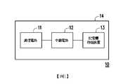
圖1是根據本發明的一範例實施例所繪示的電路參數調整系統的示意圖。請參照圖1,系統(亦稱為電路參數調整系統)10包括處理電路11、中繼電路(re-driving circuit)12及記憶體儲存裝置13。處理電路11可經由中繼電路12存取記憶體儲存裝置13。例如,處理電路11可包括中央處理單元(Central Processing Unit, CPU)、或是其他可程式化之一般用途或特殊用途的微處理器、數位訊號處理器(Digital Signal Processor, DSP)、可程式化控制器、特殊應用積體電路(Application Specific Integrated Circuits, ASIC)、可程式化邏輯裝置(Programmable Logic Device, PLD)或其他類似裝置或這些裝置的組合。FIG. 1 is a schematic diagram of a circuit parameter adjustment system according to an exemplary embodiment of the present invention. Referring to FIG. 1 , a system (also referred to as a circuit parameter adjustment system) 10 includes a
中繼電路12耦接至處理電路11與記憶體儲存裝置13。例如,中繼電路12可設置於處理電路11與記憶體儲存裝置13之間的訊號傳遞路徑上。中繼電路12可用以調變在處理電路11與記憶體儲存裝置13之間傳遞的訊號,以延長所述訊號的傳輸距離。例如,中繼電路12可包括訊號中繼器(Re-driver)。The
記憶體儲存裝置13用以非揮發性地儲存資料。例如,記憶體儲存裝置13可包括隨身碟、記憶卡、固態硬碟(Solid State Drive, SSD)或無線記憶體儲存裝置等外接式儲存裝置。或者,記憶體儲存裝置13也可包括嵌入式多媒體卡(embedded Multi Media Card, eMMC)或嵌入式多晶片封裝(embedded Multi Chip Package, eMCP)儲存裝置等嵌入式儲存裝置。The
在一範例實施例中,處理電路11與中繼電路12設置於主機板14上並經由主機板14彼此通訊。在一範例實施例中,處理電路11、中繼電路12及記憶體儲存裝置13皆設置於主機板14上並經由主機板14彼此通訊。In an exemplary embodiment, the
在一範例實施例中,記憶體儲存裝置13可藉由嵌入式的安裝方式內嵌於主機板14上。在一範例實施例中,記憶體儲存裝置13亦可以藉由高速周邊零件連接介面(Peripheral Component Interconnect Express, PCI Express)插槽、序列先進附件(Serial Advanced Technology Attachment, SATA)插槽、通用序列匯流排(Universal Serial Bus, USB)插槽或類似的匯流排插槽而可插拔式地安裝於主機板14上(即電性連接至主機板14)。In an exemplary embodiment, the
在一範例實施例中,處理電路11可經由中繼電路12傳送至少一指令至記憶體儲存裝置13。例如,所述指令可包括預先定義的開發者指令或類似指令。所述指令可用以指示記憶體儲存裝置13提供訊號品質資訊。In an exemplary embodiment, the
在一範例實施例中,所述訊號品質資訊可由記憶體儲存裝置13產生。所述訊號品質資訊可反映記憶體儲存裝置13經由中繼電路12接收到的測試訊號的訊號品質。所述測試訊號可由處理電路11產生並經由中繼電路12調變後傳送至傳送記憶體儲存裝置13。記憶體儲存裝置13可根據所接收到的測試訊號產生所述訊號品質資訊。In an exemplary embodiment, the signal quality information may be generated by the
在一範例實施例中,響應於所述指令,記憶體儲存裝置13可將所述訊號品質資訊提供給處理電路11。然後,處理電路11可根據所述訊號品質資訊調整中繼電路12的電路參數。經調整的電路參數可用以提高中繼電路12的運作效能。例如,經調整的電路參數可改善經由中繼電路12在處理電路11與記憶體儲存裝置13之間傳輸的訊號的訊號品質,從而提高中繼電路12的運作效能。In an exemplary embodiment, in response to the command, the
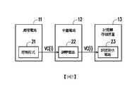
圖2至圖5是根據本發明的一範例實施例所繪示的調整中繼電路的電路參數的示意圖。請參照圖2,在一範例實施例中,處理電路11包括控制程式21,中繼電路12包括調變電路22且記憶體儲存裝置13包括訊號接收電路23。2 to 5 are schematic diagrams of adjusting circuit parameters of a relay circuit according to an exemplary embodiment of the present invention. Referring to FIG. 2 , in an exemplary embodiment, the
處理電路11可運行控制程式21以產生測試訊號TS(i)。i可以為任意正整數。測試訊號TS(i)可經由中繼電路12傳送至記憶體儲存裝置13。其中,測試訊號TS(i)可先被傳送至中繼電路12。當接收到測試訊號TS(i)時,調變電路22可根據一或多個電路參數來自動對測試訊號TS(i)進行調變。例如,所述調變可包括改變測試訊號TS(i)的電壓、波形或頻率等各式電氣特徵。經調變電路22調變的測試訊號TS(i)可被傳送至記憶體儲存裝置13。The
訊號接收電路23可經由中繼電路12接收測試訊號TS(i)。當接收到測試訊號TS(i)時,訊號接收電路23可對測試訊號TS(i)進行訊號恢復等前處理並對測試訊號TS(i)進行分析。訊號接收電路23可根據測試訊號TS(i)的分析結果產生與測試訊號TS(i)有關的訊號品質資訊(例如圖4的訊號品質資訊SQ(i))。與測試訊號TS(i)有關的訊號品質資訊可反映所接收到的測試訊號TS(i)的訊號品質。訊號接收電路23可將所述訊號品質資訊暫存於記憶體儲存裝置13中。The
請參照圖3,接續於圖2的範例實施例,在傳送測試訊號TS(i)之後,處理電路11可運行控制程式21以產生開發者指令VC(i)。開發者指令VC(i)對應於測試訊號TS(i)。處理電路11可經由中繼電路12將開發者指令VC(i)傳送至記憶體儲存裝置13。開發者指令VC(i)可用以指示記憶體儲存裝置13提供與測試訊號TS(i)有關的訊號品質資訊。Referring to FIG. 3 , following the exemplary embodiment of FIG. 2 , after transmitting the test signal TS(i), the
請參照圖4,接續於圖3的範例實施例,在接收到開發者指令VC(i)之後,響應於開發者指令VC(i),記憶體儲存裝置13可讀取先前儲存的與測試訊號TS(i)有關的訊號品質資訊SQ(i)。此外,響應於開發者指令VC(i),記憶體儲存裝置13可經由中繼電路12將訊號品質資訊SQ(i)傳送至處理電路11。Referring to FIG. 4 , following the exemplary embodiment of FIG. 3 , after receiving the developer command VC(i), the
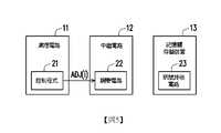
請參照圖5,接續於圖4的範例實施例,在接收到訊號品質資訊SQ(i)之後,處理電路11可根據訊號品質資訊SQ(i)獲得經由調變電路22傳送至記憶體儲存裝置13的測試訊號TS(i)的訊號品質。根據訊號品質資訊SQ(i),處理電路11可運行控制程式21發送參數調整指令ADJ(i)至中繼電路12。中繼電路12可根據參數調整指令ADJ(i)來調整調變電路22的一或多個電路參數。Referring to FIG. 5 , following the exemplary embodiment of FIG. 4 , after receiving the signal quality information SQ(i), the
在一範例實施例中,處理電路11可根據訊號品質資訊SQ(i)評估當前調變電路22所使用的電路參數是否適當(例如是否達到相對較佳的訊號傳輸品質)。若不適當(例如未達到相對較佳的訊號傳輸品質),處理電路11可運行控制程式21發送參數調整指令ADJ(i)至中繼電路12,以持續對調變電路22的一或多個電路參數進行調整。反之,若適當(例如已達到相對較佳的訊號傳輸品質),則處理電路11可不發送參數調整指令ADJ(i)。In an exemplary embodiment, the
須注意的是,圖2至圖5的範例實施例中所提及的操作可被重複執行多次,以持續根據調變電路22對測試訊號TS(i)的調變結果(或訊號品質資訊SQ(i))來調整調變電路22所使用的電路參數。例如,當i=1時,測試訊號TS(1)可先被調變電路22調變並傳送至記憶體儲存裝置13。然後,處理電路11可使用開發者指令VC(1)向記憶體儲存裝置13請求訊號品質資訊SQ(1)。訊號品質資訊SQ(1)可反映記憶體儲存裝置13所接收到的測試訊號TS(1)的訊號品質。根據記憶體儲存裝置13所提供的訊號品質資訊SQ(1),處理電路11可藉由參數調整指令ADJ(i)來調整調變電路22的特定電路參數。接著,當i=2、3或其他數值時,圖2至圖5的範例實施例中所提及的操作可被重複,直到完成對調變電路22的參數調整操作。It should be noted that, the operations mentioned in the exemplary embodiments of FIG. 2 to FIG. 5 can be repeatedly performed for many times, so as to continue according to the modulation result (or signal quality) of the test signal TS(i) by the
在一範例實施例中,中繼電路12包括接收端電路(亦稱為第一接收端電路)與發送端電路(亦稱為第一發送端電路),且記憶體儲存裝置13也包括接收端電路(亦稱為第二接收端電路)與發送端電路(亦稱為第二發送端電路)。中繼電路12中的接收端電路(即第一接收端電路)與記憶體儲存裝置13中的接收端電路(即第二接收端電路)皆屬於RX電路並用以從外部接收訊號。中繼電路12中的發送端電路(即第一發送端電路)與記憶體儲存裝置13中的發送端電路(即第二發送端電路)皆屬於TX電路並用以發送訊號。In an exemplary embodiment, the
在一範例實施例中,中繼電路12中的發送端電路(即第一發送端電路)耦接至記憶體儲存裝置13中的接收端電路(即第二接收端電路)。在一範例實施例中,中繼電路12中的發送端電路(即第一發送端電路)可發送測試訊號TS(i)至記憶體儲存裝置13中的接收端電路(即第二接收端電路)。在一範例實施例中,調變電路22可設置於第一發送端電路中。在一範例實施例中,訊號接收電路23可設置於第二接收端電路中。In an exemplary embodiment, the transmitter circuit (ie, the first transmitter circuit) in the
在一範例實施例中,在傳遞測試訊號TS(i)的過程中,中繼電路12可經由第一接收端電路從處理電路11接收測試訊號TS(i)並經由第一發送端電路中的調變電路22來調變測試訊號TS(i)。經調變的測試訊號TS(i)可經由第一發送端電路傳送至記憶體儲存裝置13。記憶體儲存裝置13可經由第二接收端電路中的訊號接收電路23接收測試訊號TS(i)並產生對應於測試訊號TS(i)的訊號品質資訊SQ(i)。訊號品質資訊SQ(i)可經由第二發送端電路傳送至中繼電路12並經由中繼電路12傳送至處理電路11。然後,處理電路11可根據訊號品質資訊SQ(i)發送參數調整指令ADJ(i)至中繼電路12,以藉由參數調整指令ADJ(i)來調整第一發送端電路的至少一設定參數。例如,中繼電路12中經調整的設定參數可包括第一發送端電路(或調變電路22)中的訊號放大器的設定參數等可改變由第一發送端電路輸出的訊號的電壓、波形或頻率等各式電氣特徵之參數。此外,記憶體儲存裝置13中的發送端電路(即第二發送端電路)及/或接收端電路(即第二接收端電路)的至少一設定參數是由記憶體儲存裝置13本身進行設定及/或調整。例如,記憶體儲存裝置13中經調整的設定參數可包括第二接收端電路(或訊號接收電路23)中的等化器電路的設定參數。In an exemplary embodiment, in the process of transmitting the test signal TS(i), the
在一範例實施例中,在將中繼電路12與記憶體儲存裝置13電性連接至主機板14之後,處理電路11可運行控制程式21以對中繼電路12執行一初始化設定。例如,在此初始化設定中,控制程式21可指示中繼電路12執行一初始化配置,以將中繼電路12的至少部分參數設定為初始值。在完成初始化設定後,處理電路11可運行控制程式21以經由初始化後的中繼電路12與記憶體儲存裝置13執行交握程序(亦稱為交握操作)。在此交握程序中,處理電路11可經由中繼電路12與記憶體儲存裝置13交換資訊,例如交換與電壓及/或頻率有關的電氣資訊。此外,在此交握程序中,記憶體儲存裝置13可根據來自中繼電路12的資訊自動調整記憶體儲存裝置13中的接收端電路(即第二接收端電路)(例如訊號接收電路23)的至少一設定參數。在完成交握程序後,處理電路11可運行控制程式21以執行圖2至圖5的範例實施例中提及的至少部分操作。此外,在一範例實施例中,圖2的範例實施例中提及的至少部分操作(例如傳送測試訊號TS(i)並分析測試訊號TS(i)的訊號品質)亦可在所述交握程序中執行。In an exemplary embodiment, after the
在一範例實施例中,訊號接收電路23可根據所接收到的測試訊號TS(i)來評估測試訊號TS(i)的訊號恢復狀態、訊號眼寬狀態、訊號眼高狀態及/或訊號邊緣狀態。例如,訊號接收電路23可包括眼寬偵測器及/或眼高偵測器等各式用以評估訊號品質的檢測電路。然後,訊號接收電路23可根據評估結果儲存與測試訊號TS(i)有關的訊號品質資訊SQ(i)。藉此,所儲存的訊號品質資訊SQ(i)可反映所接收到的測試訊號TS(i)的訊號恢復狀態、訊號眼寬狀態、訊號眼高狀態及訊號邊緣狀態的至少其中之一。In an exemplary embodiment, the
圖6是根據本發明的一範例實施例所繪示的訊號的眼圖的示意圖。請參照圖6,接續於圖2的範例實施例,在一範例實施例中,訊號接收電路23可描繪出所接收到的測試訊號TS(i)的眼圖61。眼圖61中的至少部分資訊可反映所接收到的測試訊號TS(i)的訊號品質。FIG. 6 is a schematic diagram of an eye diagram of a signal according to an exemplary embodiment of the present invention. Referring to FIG. 6 , continuing from the exemplary embodiment of FIG. 2 , in an exemplary embodiment, the
在一範例實施例中,訊號接收電路23可根據眼圖61中的參數D(1)~D(5)或者其他有用的資訊來產生訊號品質資訊SQ(i)。例如,參數D(1)可反映所接收到的測試訊號TS(i)的訊號眼寬狀態。例如,參數D(2)可反映所接收到的測試訊號TS(i)的訊號眼高狀態。例如,參數D(3)~D(5)可反映所接收到的測試訊號TS(i)的訊號邊緣狀態。此外,在一範例實施例中,訊號接收電路23也可根據對所接收到的測試訊號TS(i)進行訊號恢復或訊號重建的次數來評估所接收到的測試訊號TS(i)的訊號恢復狀態。In an exemplary embodiment, the
圖7是根據本發明的一範例實施例所繪示的記憶體儲存裝置的示意圖。請參照圖7,記憶體儲存裝置13包括連接介面單元701、記憶體控制電路單元702與可複寫式非揮發性記憶體模組703。FIG. 7 is a schematic diagram of a memory storage device according to an exemplary embodiment of the present invention. Referring to FIG. 7 , the
連接介面單元701用以將記憶體儲存裝置13耦接至圖1的處理電路11、中繼電路12及/或主機板14。記憶體儲存裝置13可透過連接介面單元701與處理電路11、中繼電路12及/或主機板14通訊。例如,連接介面單元701可相容SATA標準、並列先進附件(Parallel Advanced Technology Attachment, PATA)標準、電氣和電子工程師協會(Institute of Electrical and Electronic Engineers, IEEE)1394標準、PCI Express標準、USB標準、安全數位(Secure Digital, SD)介面標準、超高速一代(Ultra High Speed-I, UHS-I)介面標準、超高速二代(Ultra High Speed-II, UHS-II)介面標準、記憶棒(Memory Stick, MS)介面標準、MCP介面標準、MMC介面標準、eMMC介面標準、通用快閃記憶體(Universal Flash Storage, UFS)介面標準、eMCP介面標準、小型快閃(Compact Flash, CF)介面標準、整合式驅動電子介面(Integrated Device Electronics, IDE)標準或其他適合的標準。此外,連接介面單元701可與記憶體控制電路單元702封裝在一個晶片中或者佈設於包含記憶體控制電路單元702的晶片外。The
記憶體控制電路單元702用以執行以硬體型式或韌體型式實作的多個邏輯閘或控制指令並且根據主機系統的指令在可複寫式非揮發性記憶體模組703中進行資料的寫入、讀取與抹除等運作。The memory
可複寫式非揮發性記憶體模組703是耦接至記憶體控制電路單元702並且用以儲存處理電路11所寫入之資料。例如,可複寫式非揮發性記憶體模組703可以是單階記憶胞(Single Level Cell, SLC)NAND型快閃記憶體模組(即,一個記憶胞中可儲存1個位元的快閃記憶體模組)、二階記憶胞(Multi Level Cell, MLC)NAND型快閃記憶體模組(即,一個記憶胞中可儲存2個位元的快閃記憶體模組)、三階記憶胞(Triple Level Cell,TLC)NAND型快閃記憶體模組(即,一個記憶胞中可儲存3個位元的快閃記憶體模組)、四階記憶胞(Quad Level Cell,QLC)NAND型快閃記憶體模組(即,一個記憶胞中可儲存4個位元的快閃記憶體模組)、其他快閃記憶體模組或其他具有相同特性的記憶體模組。The rewritable
在一範例實施例中,記憶體控制電路單元702亦稱為快閃記憶體控制器。在一範例實施例中,可複寫式非揮發性記憶體模組703亦稱為快閃記憶體模組。在一範例實施例中,圖1的主機板14上的至少部分電子電路(包含處理電路11)亦可統稱為主機系統。In an exemplary embodiment, the memory
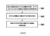
圖8是根據本發明的一範例實施例所繪示的電路參數調整方法的流程圖。請參照圖8,在步驟S801中,經由中繼電路傳送至少一指令至記憶體儲存裝置,其中所述指令用以指示所述記憶體儲存裝置提供訊號品質資訊。在步驟S802中,從所述記憶體儲存裝置接收所述訊號品質資訊。在步驟S803中,根據所述訊號品質資訊調整所述中繼電路的一或多個電路參數。FIG. 8 is a flowchart of a method for adjusting circuit parameters according to an exemplary embodiment of the present invention. Referring to FIG. 8 , in step S801 , at least one command is sent to a memory storage device through a relay circuit, wherein the command is used to instruct the memory storage device to provide signal quality information. In step S802, the signal quality information is received from the memory storage device. In step S803, one or more circuit parameters of the relay circuit are adjusted according to the signal quality information.
然而,圖8中各步驟已詳細說明如上,在此便不再贅述。值得注意的是,圖8中各步驟可以實作為多個程式碼或是電路,本發明不加以限制。此外,圖8的方法可以搭配以上範例實施例使用,也可以單獨使用,本發明不加以限制。However, each step in FIG. 8 has been described in detail as above, and will not be repeated here. It should be noted that each step in FIG. 8 can be implemented as a plurality of codes or circuits, which is not limited by the present invention. In addition, the method of FIG. 8 can be used in conjunction with the above exemplary embodiments, or can be used alone, which is not limited in the present invention.
綜上所述,在處理電路(例如CPU)經由中繼電路耦接至記憶體儲存裝置的使用情景中,處理電路可使用特定指令(例如開發者指令)來從記憶體儲存裝置讀取訊號品質資訊。然後,處理電路可根據此訊號品質資訊評估當前中繼電路所使用的電路參數是否需更新並可動態調整所述電路參數。在一範例實施例中,不需額外外接檢測儀器來對中繼電路輸出的訊號進行檢測。藉由處理電路與記憶體儲存裝置之間的配合,中繼電路使用的電路參數可適當地被調整,從而提高對於中繼電路使用的電路參數的調整效率。To sum up, in a usage scenario where a processing circuit (eg, a CPU) is coupled to a memory storage device via a relay circuit, the processing circuit can use a specific command (eg, a developer command) to read signals from the memory storage device quality information. Then, the processing circuit can evaluate whether the circuit parameters currently used by the relay circuit need to be updated according to the signal quality information and can dynamically adjust the circuit parameters. In an exemplary embodiment, no additional external detection instrument is required to detect the signal output by the relay circuit. Through the cooperation between the processing circuit and the memory storage device, the circuit parameters used by the relay circuit can be adjusted appropriately, thereby improving the adjustment efficiency of the circuit parameters used by the relay circuit.
雖然本發明已以實施例揭露如上,然其並非用以限定本發明,任何所屬技術領域中具有通常知識者,在不脫離本發明的精神和範圍內,當可作些許的更動與潤飾,故本發明的保護範圍當視後附的申請專利範圍所界定者為準。Although the present invention has been disclosed above by the embodiments, it is not intended to limit the present invention. Anyone with ordinary knowledge in the technical field can make some changes and modifications without departing from the spirit and scope of the present invention. Therefore, The protection scope of the present invention shall be determined by the scope of the appended patent application.
10:電路參數調整系統 11:處理電路 12:中繼電路 13:記憶體儲存裝置 14:主機板 21:控制程式 22:調變電路 23:訊號接收電路 61:眼圖 701:連接介面單元 702:記憶體控制電路單元 703:可複寫式非揮發性記憶體模組 S801:步驟(經由中繼電路傳送指令至記憶體儲存裝置,其中所述指令用以指示記憶體儲存裝置提供訊號品質資訊) S802:步驟(從所述記憶體儲存裝置接收所述訊號品質資訊) S803:步驟(根據所述訊號品質資訊調整所述中繼電路的電路參數)10: Circuit parameter adjustment system 11: Processing circuit 12: Relay circuit 13: Memory storage device 14: Motherboard 21: Control program 22: Modulation circuit 23: Signal receiving circuit 61: Eye Diagram 701: Connection interface unit 702: Memory control circuit unit 703: Rewritable non-volatile memory module S801: Step (transmitting an instruction to a memory storage device via a relay circuit, wherein the instruction is used to instruct the memory storage device to provide signal quality information) S802: Step (receive the signal quality information from the memory storage device) S803: Step (adjust the circuit parameters of the relay circuit according to the signal quality information)
圖1是根據本發明的一範例實施例所繪示的電路參數調整系統的示意圖。 圖2至圖5是根據本發明的一範例實施例所繪示的調整中繼電路的電路參數的示意圖。 圖6是根據本發明的一範例實施例所繪示的訊號的眼圖的示意圖。 圖7是根據本發明的一範例實施例所繪示的記憶體儲存裝置的示意圖。 圖8是根據本發明的一範例實施例所繪示的電路參數調整方法的流程圖。FIG. 1 is a schematic diagram of a circuit parameter adjustment system according to an exemplary embodiment of the present invention. 2 to 5 are schematic diagrams of adjusting circuit parameters of a relay circuit according to an exemplary embodiment of the present invention. FIG. 6 is a schematic diagram of an eye diagram of a signal according to an exemplary embodiment of the present invention. FIG. 7 is a schematic diagram of a memory storage device according to an exemplary embodiment of the present invention. FIG. 8 is a flowchart of a method for adjusting circuit parameters according to an exemplary embodiment of the present invention.
10:電路參數調整系統10: Circuit parameter adjustment system
11:處理電路11: Processing circuit
12:中繼電路12: Relay circuit
13:記憶體儲存裝置13: Memory storage device
14:主機板14: Motherboard
Claims (22)
Translated fromChinesePriority Applications (1)
| Application Number | Priority Date | Filing Date | Title |
|---|---|---|---|
| TW110113876ATWI762274B (en) | 2021-04-19 | 2021-04-19 | System and method for adjusting circuit parameter and host system |
Applications Claiming Priority (1)
| Application Number | Priority Date | Filing Date | Title |
|---|---|---|---|
| TW110113876ATWI762274B (en) | 2021-04-19 | 2021-04-19 | System and method for adjusting circuit parameter and host system |
Publications (2)
| Publication Number | Publication Date |
|---|---|
| TWI762274Btrue TWI762274B (en) | 2022-04-21 |
| TW202242661A TW202242661A (en) | 2022-11-01 |
Family
ID=82199028
Family Applications (1)
| Application Number | Title | Priority Date | Filing Date |
|---|---|---|---|
| TW110113876ATWI762274B (en) | 2021-04-19 | 2021-04-19 | System and method for adjusting circuit parameter and host system |
Country Status (1)
| Country | Link |
|---|---|
| TW (1) | TWI762274B (en) |
Citations (6)
| Publication number | Priority date | Publication date | Assignee | Title |
|---|---|---|---|---|
| CN1716227A (en)* | 2004-06-30 | 2006-01-04 | 富士通株式会社 | Operating means and operation apparatus control method, program and computer-readable medium |
| CN101937408A (en)* | 2009-06-25 | 2011-01-05 | 精工爱普生株式会社 | Integrated circuit system, data writing method, and data reading method |
| US20140223068A1 (en)* | 2005-09-26 | 2014-08-07 | Rambus Inc. | Memory System Topologies Including A Buffer Device And An Integrated Circuit Memory Device |
| US20170285941A1 (en)* | 2016-04-01 | 2017-10-05 | Intel Corporation | Read delivery for memory subsystem with narrow bandwidth repeater channel |
| CN108701108A (en)* | 2016-04-01 | 2018-10-23 | 英特尔公司 | Memory sub-system with narrow bandwidth repeater channel |
| TW201947414A (en)* | 2017-10-20 | 2019-12-16 | 慧榮科技股份有限公司 | Storage device and interface chip thereof |
- 2021
- 2021-04-19TWTW110113876Apatent/TWI762274B/enactive
Patent Citations (6)
| Publication number | Priority date | Publication date | Assignee | Title |
|---|---|---|---|---|
| CN1716227A (en)* | 2004-06-30 | 2006-01-04 | 富士通株式会社 | Operating means and operation apparatus control method, program and computer-readable medium |
| US20140223068A1 (en)* | 2005-09-26 | 2014-08-07 | Rambus Inc. | Memory System Topologies Including A Buffer Device And An Integrated Circuit Memory Device |
| CN101937408A (en)* | 2009-06-25 | 2011-01-05 | 精工爱普生株式会社 | Integrated circuit system, data writing method, and data reading method |
| US20170285941A1 (en)* | 2016-04-01 | 2017-10-05 | Intel Corporation | Read delivery for memory subsystem with narrow bandwidth repeater channel |
| CN108701108A (en)* | 2016-04-01 | 2018-10-23 | 英特尔公司 | Memory sub-system with narrow bandwidth repeater channel |
| TW201947414A (en)* | 2017-10-20 | 2019-12-16 | 慧榮科技股份有限公司 | Storage device and interface chip thereof |
Also Published As
| Publication number | Publication date |
|---|---|
| TW202242661A (en) | 2022-11-01 |
Similar Documents
| Publication | Publication Date | Title |
|---|---|---|
| US10326622B2 (en) | Equalizer tuning method, signal receiving circuit and a memory storage device | |
| US9467314B1 (en) | Signal modulation method, adaptive equalizer and memory storage device | |
| KR20130042370A (en) | Test method for ufs interface and memory device testing by the same method | |
| TWI467379B (en) | System operation method, and memory controller and memory storage device using the same | |
| US20140185388A1 (en) | Dynamic drive strength optimization | |
| US11023138B2 (en) | Management operations in predictable latency mode | |
| US8984250B2 (en) | Memory controller, memory device and method for determining type of memory device | |
| CN106448719A (en) | Signal modulation method, adaptive equalizer and memory storage device | |
| KR102835513B1 (en) | Memory system and operation method thereof | |
| TWI534607B (en) | Memory control circuit unit, data transmitting method and memory storage apparatus | |
| TWI640872B (en) | Memory control circuit unit, memory storage device and control method thereof | |
| WO2021098210A1 (en) | Margin detection method and apparatus for data signal, and storage device | |
| KR20240016884A (en) | Storage system, storage device and method for controlling the system | |
| TWI762274B (en) | System and method for adjusting circuit parameter and host system | |
| CN117495371A (en) | Storage system, storage device and method of controlling storage system | |
| CN103383663B (en) | System operation method, memory controller and memory | |
| US11636902B2 (en) | Signal modulation apparatus, memory storage apparatus, and signal modulation method | |
| CN113206683A (en) | Circuit parameter adjusting system, method and host system | |
| CN115223624A (en) | Method for operating host device and memory device and vehicle including the same | |
| TWI587145B (en) | Channel switching device, memory storage device and channel switching method | |
| US11726698B2 (en) | Data logging sub-system for memory sub-system controller | |
| KR20240166167A (en) | A integrated circuit, opearting method of the same and a memory system | |
| CN106611608A (en) | Memory control circuit unit, memory storage device and data transmission method | |
| US12282353B2 (en) | Clock control circuit module, memory storage device and clock control method | |
| CN109698003A (en) | Eqalizing cricuit adjusting process, signal receiving circuit and memory storage apparatus |