Movatterモバイル変換


[0]ホーム

URL:


TWI760255B - Detection method and detection pattern unit of semiconductor patterning process - Google Patents

Detection method and detection pattern unit of semiconductor patterning process
Download PDF

Info

Publication number
TWI760255B
TWI760255BTW110123365ATW110123365ATWI760255BTW I760255 BTWI760255 BTW I760255BTW 110123365 ATW110123365 ATW 110123365ATW 110123365 ATW110123365 ATW 110123365ATW I760255 BTWI760255 BTW I760255B
Authority
TW
Taiwan
Prior art keywords
detection
extension
main body
patterns
patterning process
Prior art date
Application number
TW110123365A
Other languages
Chinese (zh)
Other versions
TW202300901A (en
Inventor
黃天興
Original Assignee
黃天興
Priority date (The priority date is an assumption and is not a legal conclusion. Google has not performed a legal analysis and makes no representation as to the accuracy of the date listed.)
Filing date
Publication date
Application filed by 黃天興filedCritical黃天興
Priority to TW110123365ApriorityCriticalpatent/TWI760255B/en
Application grantedgrantedCritical
Publication of TWI760255BpublicationCriticalpatent/TWI760255B/en
Publication of TW202300901ApublicationCriticalpatent/TW202300901A/en

Links

Images

Landscapes

Abstract

Translated fromChinese

本發明提供一種可用於半導體圖案化製程的檢測方法,包含一量測步驟、一計算步驟,及一比對步驟。重複量測於相同或不同的一半導體基材上,經由圖案化製程後產生之相同的多個檢測圖案的至少兩個間距,並將每一次之圖案化製程量得的間距進行四則運算,得到多個對應該等不同次之圖案化製程的監測值,再利用該等監測值獲得一與時間或者量測晶圓片號位置相關的監測曲線或將該等監測值與一預設值比對,得到該等檢測圖案的關鍵尺寸變化或黃光製程聚焦(focus)的檢測結果。此外,本發明還提供一種用於該檢測方法的檢測圖案單元。The present invention provides a detection method applicable to a semiconductor patterning process, which includes a measurement step, a calculation step, and a comparison step. Repeatedly measuring at least two spacings of the same plurality of detection patterns generated after the patterning process on the same or different semiconductor substrates, and performing four arithmetic operations on the spacings measured in each patterning process to obtain A plurality of monitoring values corresponding to the patterning process of different times, and then use the monitoring values to obtain a monitoring curve related to time or the position of the measured wafer number or compare the monitoring values with a preset value , to obtain the detection results of the critical dimension change of the detection patterns or the focus of the yellow light process. In addition, the present invention also provides a detection pattern unit for the detection method.

Description

Translated fromChinese
半導體圖案化製程的檢測方法及檢測圖案單元Detection method and detection pattern unit of semiconductor patterning process

本發明是有關於一種半導體製程的檢測方法,及檢測用的圖案,特別是指一種用於半導體圖案化製程的檢測方法及檢測圖案單元。The present invention relates to a detection method for a semiconductor manufacturing process and a detection pattern, in particular to a detection method and a detection pattern unit for a semiconductor patterning process.

關鍵尺寸(Critical Dimension,CD)是用於評估半導體圖案化製程,如微影、蝕刻製程的圖案化精度。由於半導體製程技術發展迅速,節距以及溝槽等關鍵尺寸的要求越來越高,因此,在積層化製程過程,若形成的積層圖案的關鍵尺寸產生誤差時,將會使製成的元件特性無法達到預期目標,尤其在積體電路加工技術已進步至奈米級的現在,如何控制奈米級結構的關鍵尺寸,更是越顯重要,因此,如何監控並檢測圖案化製程過程產生之積層圖案的關鍵尺寸,以對各個圖案化製程進行監控,是半導體製程中極重要的目標。Critical Dimension (CD) is used to evaluate the patterning accuracy of semiconductor patterning processes, such as lithography and etching processes. Due to the rapid development of semiconductor process technology, the requirements for key dimensions such as pitch and trench are getting higher and higher. Therefore, during the build-up process, if there is an error in the key dimensions of the formed build-up pattern, the characteristics of the fabricated device will be degraded. Unable to achieve the expected goal, especially now that the integrated circuit processing technology has advanced to the nano-scale, how to control the key dimensions of the nano-scale structure is more and more important. Therefore, how to monitor and detect the build-up generated during the patterning process. The critical dimension of the pattern to monitor each patterning process is a very important goal in the semiconductor process.

因此,本發明之目的,即在提供一種用於監測半導體圖案化製程的檢測方法。Therefore, an object of the present invention is to provide a detection method for monitoring a semiconductor patterning process.

於是,本發明檢測方法包含一量測步驟、一計算步驟,及一比對步驟。Therefore, the detection method of the present invention includes a measurement step, a calculation step, and a comparison step.

該量測步驟是重複量測於相同或不同的一半導體基材上,經由圖案化製程後產生之相同的多個檢測圖案於相同位置的至少兩個間距,該至少兩個間距是由具有不同線路密度的檢測圖案所產生,得到多組對應不同次之圖案化製程的檢測數據,且每一組檢測數據包含至少兩個間距。The measuring step is to repeatedly measure at least two spacings of the same plurality of detection patterns at the same position on the same or different semiconductor substrates after the patterning process, and the at least two spacings are made of different spacings. The detection pattern of the line density is generated, and a plurality of sets of detection data corresponding to different patterning processes are obtained, and each set of detection data includes at least two pitches.

該計算步驟是將每一次圖案化製程量得的檢測數據進行四則運算,得到多個對應該等不同次之圖案化製程的監測值。The calculation step is to perform four arithmetic operations on the detection data measured in each patterning process, and obtain a plurality of monitoring values corresponding to the patterning process with different levels.

該比對步驟是利用該等監測值獲得一與檢測圖案形成時間、量測位置,及量測晶圓片號其中至少一者相關的監測曲線或將該等監測值與一預設值比對,得到該等檢測圖案單元與關鍵尺寸變化相關的檢測結果。The comparison step is to obtain a monitoring curve related to at least one of the detection pattern formation time, the measurement position, and the measurement wafer number by using the monitoring values, or compare the monitoring values with a preset value , to obtain the detection results related to the critical dimension change of the detection pattern units.

此外,本發明之另一目的,即在提供一種用於監測半導體圖案化製程的檢測圖案單元。In addition, another object of the present invention is to provide a detection pattern unit for monitoring a semiconductor patterning process.

於是,本發明該檢測圖案單元包含:至少兩個沿同一方向間隔排列的檢測圖案。Therefore, the detection pattern unit of the present invention comprises: at least two detection patterns arranged at intervals along the same direction.

每一個檢測圖案均具有一沿與該第一方向相交的一第二方向延伸的主體部,且該等檢測圖案的其中至少一者具有一位於與相應的該主體部的其中至少一表面的延伸部,該延伸部具有多個彼此間隔排列的延伸段。且該等延伸段可沿該第一方向與相應的該主體部的表面間隔排列,或自相應的主體部的表面沿該第二方向間隔排列,而可令該等檢測圖案產生至少兩個由不同線路密度造成的間距。Each detection pattern has a main body portion extending in a second direction intersecting the first direction, and at least one of the detection patterns has an extension located on at least one surface of the corresponding main body portion part, the extension has a plurality ofExtensions spaced apart from each other. And the extension sections can be spaced apart from the surface of the corresponding main body part along the first direction, or spaced from the surface of the corresponding main body part along the second direction, so that the detection patterns can generate at least two Spacing due to different line densities.

本發明之功效在於:透過檢測圖案的設計,並利用量測得到該等檢測圖案所產生的至少兩個間距,利用將該至少兩個間距進行計算後,得到與該等檢測圖案於不同圖案化製程的關鍵尺寸變化相關的監測值,從而可透過對該等監測值對圖案化製程進行監控。The effect of the present invention is that: through the design of the detection patterns, at least two distances generated by the detection patterns are obtained by measurement, and after the at least two distances are calculated, the patterns in different patterns from the detection patterns are obtained. Monitoring values related to critical dimension changes of the process, so that the patterning process can be monitored through these monitoring values.

2:檢測圖案單元2: Detection pattern unit

21、21A、21B:檢測圖案21, 21A, 21B: Detection pattern

211:主體部211: main body

212:延伸部212: Extensions

212A、212B:延伸段212A, 212B: Extensions

a~f:間距a~f: spacing

A~D:間距A~D: Spacing

B1~B3:監測值B1 ~B3 : Monitoring value

F1~F3:焦距F1 ~F3 : Focal length

P:對位圖案單元P: alignment pattern unit

P1:第一對位圖案P1: The first alignment pattern

P11:第一圖案P11: The first pattern

P2:第二對位圖案P2: Second alignment pattern

P21:第二圖案P21: Second pattern

本發明之其他的特徵及功效,將於參照圖式的實施方式中清楚地呈現,其中:圖1是一文字流程圖,說明本發明關鍵尺寸偏移檢測方法的一實施例;圖2是一示意圖,說明用於該實施例的檢測圖案單元;圖3是一示意圖,說明該檢測圖案單元的另一結構態樣;圖4是一示意圖,說明該檢測圖案單元的又一結構態樣;圖5是一示意圖,輔助說明該量測步驟;圖6是一示意圖,輔助說明該比對步驟;圖7是一示意圖,輔助說明該比對步驟的另一比對方式;圖8是一示意圖,輔助說明利用該比對步驟的結果監測檢測圖案的邊緣粗糙度,以及線寬粗糙度;圖9是一示意圖,說明該檢測圖案單元與檢測圖案單元整合的結構態樣;及圖10是一示意圖,說明該檢測圖案單元與檢測圖案單元整合的另一種結構態樣。Other features and effects of the present invention will be clearly presented in the embodiments with reference to the drawings, wherein: FIG. 1 is a text flow chart illustrating an embodiment of the critical dimension offset detection method of the present invention; FIG. 2 is a schematic diagram , to illustrate the detection pattern unit used in this embodiment; FIG. 3 is a schematic diagram illustrating another structural aspect of the detection pattern unit; FIG. 4 is a schematic diagram illustrating another structural aspect of the detection pattern unit; FIG. 5 is a schematic diagram to assist in explaining the measurement step; FIG. 6 is a schematic diagram to assist in explaining the comparison step;FIG. 7 is a schematic diagram illustrating another comparison method of the comparison step; FIG. 8 is a schematic diagram illustrating the edge roughness and line width roughness of the detection pattern monitored using the results of the comparison step; FIG. 9 It is a schematic diagram illustrating a structural aspect of the integration of the detection pattern unit and the detection pattern unit; and FIG. 10 is a schematic diagram illustrating another structural aspect of the integration of the detection pattern unit and the detection pattern unit.

本發明的檢測方法是藉由重複量測於相同或不同的一半導體基材上,經由圖案化製程後產生之相同的多個檢測圖案於相同位置的至少兩個間距,得到多組對應不同次之圖案化製程的檢測數據,其中,每一組檢測數據包含於同一次圖案化製程量得的至少兩個間距。再透過將該等檢測數據進行四則運算得到檢測圖案於對應不同次之圖案化製程,與關鍵尺寸變化及/或黃光製程聚焦(focus)偏移相關的多個監測值,而可透過該等監測值監控每一次圖案化製程,以確保製程的穩定性。The detection method of the present invention is to obtain a plurality of sets corresponding to different times by repeatedly measuring at least two spacings of the same multiple detection patterns generated after the patterning process on the same or different semiconductor substrates at the same position. The detection data of the patterning process, wherein each set of detection data includes at least two pitches measured in the same patterning process. Then, by performing four arithmetic operations on the inspection data, the inspection patterns corresponding to different sub-patterning processes, a plurality of monitoring values related to the critical dimension change and/or the focus shift of the yellow light process, can be obtained through these inspection data. The monitoring value monitors each patterning process to ensure the stability of the process.

茲以下述實施例說明本發明的檢測方法。The following examples are used to illustrate the detection method of the present invention.

參閱圖1,本發明檢測方法的一實施例包含:一量測步驟31、一計算步驟32,及一比對步驟33。Referring to FIG. 1 , an embodiment of the detection method of the present invention includes: a measurement step 31 , acalculation step 32 , and acomparison step 33 .

該量測步驟31是重複量測於相同或不同的一半導體基材(圖未示)上,經由圖案化製程後產生之檢測圖案單元於相同位置的至少兩個間距,以得到多組對應不同次之圖案化製程的檢測數據,且每一組檢測數據包含同一次圖案化製程量得的至少兩個間距。The measuring step 31 is to repeatedly measure at least two spacings at the same position of the detection pattern units generated after the patterning process on the same or different semiconductor substrates (not shown), so as to obtain a plurality of sets of corresponding different Next is the detection data of the patterning process, and each set of detection data includes at least two pitches measured in the same patterning process.

該基材可以是半導體晶圓、光罩、玻璃基板,或具有微米或奈米尺寸結構的基板,該圖案化製程可以是微影或蝕刻等製程。The substrate can be a semiconductor wafer, a photomask, a glass substrate, or a substrate with a micro or nano-sized structure, and the patterning process can be a process such as lithography or etching.

該量測步驟31為透過一可感應或讀取光學影像的光學取像裝置取得於每次圖案化製程後形成於該半導體基材的檢測圖案單元的影像,並選取該檢測圖案單元相同的位置進行該至少兩個間距的量測。The measuring step 31 is to obtain an image of the detection pattern unit formed on the semiconductor substrate after each patterning process through an optical imaging device that can sense or read optical images, and select the same position of the detection pattern unit Measurements of the at least two spacings are made.

該檢測圖案單元2可包含多個沿第一方向X及/或第二方向Y間隔排列的檢測圖案21。Thedetection pattern unit 2 may include a plurality ofdetection patterns 21 arranged at intervals along the first direction X and/or the second direction Y.

要說明的是,由於圖案化製程的各種參數影響,所以,形成於該半導體基材上的檢測圖案21相對原始於該光罩上的檢測圖案21,會有各種尺寸或形狀的誤差產生,因此,為了便於說明相關檢測圖案21的結構及量測方式,本案用於說明該實施例的相關檢測圖案單元2,除非有特別說明,否則均是以位於光罩的該檢測圖案單元2(on mask)為例。而本案的檢測方法實際量測的對象則是利用具有該檢測圖案單元2的光罩經過圖案化製程後形成於半導體基材(如晶片)上的該檢測圖案單元2(on wafer)。It should be noted that, due to the influence of various parameters of the patterning process, thedetection pattern 21 formed on the semiconductor substrate will have various size or shape errors compared to thedetection pattern 21 on the original mask. Therefore, , in order to facilitate the description of the structure and measurement method of therelevant detection pattern 21, this case is used to describe the relevantdetection pattern unit 2 of this embodiment. Unless otherwise specified, the detection pattern unit 2 (on mask ) as an example. The actual measurement object of the detection method in this case isThe inspection pattern unit 2 (on wafer) is formed on a semiconductor substrate (eg, a wafer) after a patterning process using a photomask having theinspection pattern unit 2 .

參閱圖2,圖2是以位於光罩的該檢測圖案單元2(on mask),且是以該檢測圖案單元2的其中兩個沿一第一方向X隔排列的一檢測圖案21A,及一檢測圖案21B為例說明。Referring to FIG. 2, FIG. 2 shows the detection pattern unit 2 (on mask) located on the mask, and two of thedetection pattern units 2 are arranged along a first direction X at intervals of adetection pattern 21A, and a Thedetection pattern 21B will be described as an example.

該檢測圖案21A、21B均具有沿一第二方向Y延伸的一主體部211,其中,該檢測圖案21A具有一位於與相應的該主體部211的其中一表面的延伸部212,且該延伸部212是由多個自該主體部211的表面彼此等間隔排列(相同線距)的延伸段212A共同構成且該等延伸段212A具有相同的沿伸長度及寬度(線寬)。該檢測圖案21B具有自相應的該主體部211相對該檢測圖案21A的表面設置的延伸部212,且該檢測圖案21B的延伸部212分別是由多個自該主體部211的表面彼此等間隔排列(相同線距)的延伸段212B共同構成,且該等延伸段212B具有相同的沿伸長度及寬度(線寬)。要說明的是,圖2(a)是以該檢測圖案21A、21B兩兩相對,且相對的該兩個檢測圖案21A、21B的該等延伸段212A、212B具有相同的線寬及線距相對。然,實際實施時,彼此相對的該檢測圖案21A、檢測圖案21B的該等延伸段212A、212B也可如圖2(b)所示,該等延伸段212A、212B也可彼此錯位相對;或是,可如圖2(c)所示,該等各自形成於該檢測圖案21A、21B的表面的延伸段212A、212B,可以完全佔滿(如212A)或是僅形成於該主體部211的部份表面(如212B),或是,可如圖2(d)所示,該檢測圖案21A、21B也可以只有其中一者具有該延伸部212,或是圖2(e)所示,該檢測圖案21A、21B均未設置該該延伸部212,或是如圖2(f)所示,分別自該兩個主體部211相對的兩表面延伸的延伸部212,是各自具有多個沿該第一方向X及該第二方向Y間隔延伸排列的延伸段212A、212B,而具有類似格柵結構。Each of thedetection patterns 21A and 21B has amain body portion 211 extending along a second direction Y, wherein thedetection pattern 21A has anextension portion 212 located on one surface of themain body portion 211 , and theextension portion 212 is composed of a plurality ofextension sections 212A which are arranged at equal intervals (same line spacing) from the surface of themain body 211 , and theextension sections 212A have the same extension length and width (line width). Thedetection pattern 21B hasextension parts 212 disposed from the correspondingmain body part 211 opposite to the surface of thedetection pattern 21A, and theextension parts 212 of thedetection pattern 21B are respectively formed by a plurality ofextension parts 212 arranged from the surface of themain body part 211 at equal intervals. Theextension sections 212B (the same line spacing) are formed together, and theextension sections 212B have the same extension length and width (line width). It should be noted that, in FIG. 2( a ), thedetection patterns 21A and 21B are opposite each other, and the extendingsections 212A and 212B of the twoopposite detection patterns 21A and 21B have the same line width and line spacing. . However, in actual implementation, thedetection pattern 21A and theextension sections 212A and 212B of thedetection pattern 21B that are opposite to each other may also be as shown in FIG. 2( b ), and theextension sections 212A and 212B may also be staggered and opposed to each other; or Yes, as shown in FIG. 2( c ), theextension sections 212A, 212A and 212A respectively formed on the surface of thedetection patterns 21A and 21B.212B can be completely filled (eg 212A) or only formed on a part of the surface of the main body 211 (eg 212B), or, as shown in FIG. 2(d), thedetection patterns 21A, 21B can also be only One of them has theextension portion 212, or as shown in FIG. 2(e), thedetection patterns 21A and 21B are not provided with theextension portion 212, or as shown in FIG. 2(f), from the two The extendingportions 212 extending from two opposite surfaces of themain body portion 211 each have a plurality of extendingsegments 212A, 212B extending and extending along the first direction X and the second direction Y at intervals, and have a grid-like structure.

配合參閱圖3,於一些實施例中,彼此相對的該檢測圖案21A、21B的其中至少一者的延伸部212,也可同時設置於相應的該其中至少一者的主體部211的兩相反表面。圖3是以該檢測圖案21A的主體部211相對該檢測圖案21B的表面設有該延伸部212,而該檢測圖案21B會同時設置於相應的該主體部211的兩相反表面的延伸部212為例說明。其中,該檢測圖案21A的該等延伸部212是分別由多個自該主體部211相對該檢測圖案21B的表面延伸並沿該第二方向Y間隔排列的延伸段212A所構成,該檢測圖案21B的該等延伸部212則是分別由多個自該主體部211的兩相反表面沿該第二方向Y間隔排列的延伸段212B所構成,其中,位於該主體部211的兩相反表面的該等延伸212B,可以如圖3(a)所示,具有與該等延伸段212A相同線寬及線距,且彼此對稱;也可以如圖3(b)所示,位於該主體部211的兩相反表面的該等延伸段212B,可具有不同線寬及不同線距。或是,該檢測圖案21A、21B的其中一者也可以同時均具有分別對應該主體部211的兩個不同表面(例如相反表面或相鄰表面)設置的延伸部212,且該等延伸部212可以是如前所述具有相同或是不同的線寬、線距。如圖3(c),即是於該檢測圖案21A的該主體部211的兩個相鄰表面同時形成延伸段211A,且位於不同表面的該等延伸段211A具有不同排列密度的結構示意。Referring to FIG. 3 , in some embodiments, the extendingportions 212 of at least one of thedetection patterns 21A and 21B that are opposite to each other may also be simultaneously disposed on two opposite surfaces of themain body portion 211 of the corresponding at least one of thedetection patterns 21A and 21B. . FIG. 3 shows that themain portion 211 of thedetection pattern 21A is provided with theextension portion 212 on the surface opposite to thedetection pattern 21B, and thedetection pattern 21B is simultaneously provided on thecorresponding extension portions 212 of the two opposite surfaces of themain body portion 211 as Example description. Theextension portions 212 of thedetection pattern 21A are respectively formed by a plurality ofextension segments 212A extending from themain body portion 211 relative to the surface of thedetection pattern 21B and arranged at intervals along the second direction Y. Thedetection pattern 21B Theextension portions 212 are respectively composed of a plurality ofextension segments 212B spaced along the second direction Y from two opposite surfaces of themain body portion 211 , wherein the two opposite surfaces of themain body portion 211 are located on the two opposite surfaces. Theextension 212B may, as shown in FIG. 3( a ), have the same line width and line spacing as theextension sections 212A, and be symmetrical with each other; or, as shown in FIG. 3( b ), may be located on two opposite sides of themain body 211 Theextensions 212B of the surface may haveDifferent line widths and different line spacings. Alternatively, one of thedetection patterns 21A and 21B may also haveextension portions 212 respectively corresponding to two different surfaces (eg, opposite surfaces or adjacent surfaces) of themain body portion 211 , and theextension portions 212 It can be the same or different line width and line spacing as mentioned above. As shown in FIG. 3( c ), extending sections 211A are simultaneously formed on two adjacent surfaces of themain body 211 of thedetection pattern 21A, and the extending sections 211A on different surfaces have different arrangement densities.

參閱圖4,於另一些實施例中,該延伸部212的延伸段212、212B,除了如前所述,可以是多個自相應的該主體部211的表面沿該第一方向X延伸並沿該第二方向Y間隔排列的結構態樣外,該等延伸段212A、212B也可以是多條沿該第二方向Y延伸,與相應的該主體部211表面成一間隔並沿該第一方向X間隔排列的長條狀結構。具體的說,該等具有長條狀結構的延伸段212A、212B的設置位置,可以如圖4(a)所示,僅有該檢測圖案21B反向該檢測圖案21A的表面設有該等延伸段212B,或可如圖4(b)、(c),彼此相對並成鏡像,或是形成於同一側的表面而不相對;或是,該等延伸段212也可以自該等檢測圖案21A、21B的其中至少一者的兩個相反表面同時設置,如圖4(d)是以該等延伸段212B同時設置於該檢測圖案21B的兩個相反表面,並具有不同線寬及線距的態樣。此外,該等主體部211的不同表面也可以分設置不同結構態樣的延伸段212,如圖4(e)所示,即是在檢測圖案21A及檢測圖案21B的表面分別設置具有不同結構態樣的延伸段212A、212B。Referring to FIG. 4 , in other embodiments, the extendingsections 212 and 212B of the extendingportion 212 , except as described above, may be a plurality of extending from the surface of the correspondingmain body portion 211 along the first direction X and along the first direction X. In addition to the structure in which the second direction Y is spaced apart, the extendingsections 212A and 212B may also be a plurality of extending along the second direction Y, forming an interval with the corresponding surface of themain body 211 and extending along the first direction X Long strips arranged at intervals. Specifically, the arrangement positions of theelongated sections 212A and 212B with elongated structures can be as shown in FIG. 4( a ), and only thedetection pattern 21B is provided with the extension on the surface opposite to thedetection pattern 21A. Thesegments 212B, as shown in Fig. 4(b), (c), may be opposite to each other and mirrored, or formed on the same side surface without being opposite; or, theextended segments 212 may also be formed from thedetection patterns 21A Two opposite surfaces of at least one of 21B are arranged at the same time, as shown in FIG. 4(d), theextension sections 212B are arranged on the two opposite surfaces of thedetection pattern 21B at the same time, and have different line widths and line spacings manner. In addition, different surfaces of themain body portions 211 may also be provided withextension sections 212 with different structural aspects, as shown in FIG.The surfaces are respectively provided withextension sections 212A and 212B with different structural aspects.

也就是說,實際實施時,只要讓對應設置於主體部211表面且彼此相對的延伸段212具有相同的結構態樣及相同的線寬及線距即可,設置於不同主體部211,或是相同主體部211但位於不同表面的延伸段212,則可具有不同的結構態樣,以及不同的線寬及/或線距。That is to say, in actual implementation, as long as the extendingsections 212 correspondingly disposed on the surface of themain body portion 211 and opposite to each other have the same structural aspect and the same line width and line spacing, they can be disposed in differentmain body portions 211 , or Theextension sections 212 of the samemain body portion 211 but located on different surfaces may have different structural aspects, and different line widths and/or line spacings.

較佳地,前述該等延伸段212沿該第二方向Y的節距(pitch,線寬+線距)不大於200nm,線寬/線距(duty ratio)介於0.3~0.7,且該等延伸段212沿該第一方向X的延伸長度(如圖2、3所示之延伸段212A、212B結構態樣)不大於200nm。Preferably, the pitch (line width + line spacing) of the aforementioned extendingsections 212 along the second direction Y is not greater than 200 nm, the line width/line spacing (duty ratio) is between 0.3 and 0.7, and the The extension length of theextension section 212 along the first direction X (as shown in the structures of theextension sections 212A and 212B shown in FIGS. 2 and 3 ) is not greater than 200 nm.

要說明的是,該檢測圖案單元2可以上述檢測圖案21A、21B兩兩一組的方式排列形成,或是由多個檢測圖案21A、21B沿該第一方向X及/或該第二方向Y搭配排列,只要可透過該等檢測圖案21排列,形成至少兩個由不同線路密度的檢測圖案21構成可供量測的間距的邊界即可,亦即該至少兩個間距可取自同一列相鄰或不相鄰的檢測圖案21;也可分別取自不同列且相鄰或不相鄰的檢測圖案21;或是該至少兩個間距也可取自不同排列方向且相鄰或不相鄰的檢測圖案21。此外,要再說明的是,該至少兩個間距可以是量測經圖案化製程後實際形成於該半導體基材上,相鄰的檢測圖案21的線寬/線距(line/space),或是橫跨該等檢測圖案21(例如跨線寬(line)或跨線距(space))的間距。It should be noted that, thedetection pattern unit 2 can be formed by arranging thedetection patterns 21A, 21B in pairs, or by a plurality ofdetection patterns 21A, 21B along the first direction X and/or the second direction Y With the arrangement, as long as thedetection patterns 21 can be arranged to form at least twodetection patterns 21 with different circuit densities to form the boundary of the measurable spacing, that is, the at least two spacings can be taken from the same column phase. Adjacent ornon-adjacent detection patterns 21; can also be taken from different columns and adjacent ornon-adjacent detection patterns 21; or the at least two spacings can also be taken from different arrangement directions and adjacent or non-adjacent Thedetection pattern 21. In addition, it should be noted that the at least two distances can be measured by measuring the line width/line/space of theadjacent detection patterns 21 actually formed on the semiconductor substrate after the patterning process, or is across the detection patterns 21 (egSpacing across the line width (line) or across the line spacing (space).

較佳地,該檢測圖案單元2是令用於量測間距的該等檢測圖案21彼此相對的延伸部212具有相同的圖案。如此,藉由量測具有相同佈局圖案之延伸部212的該檢測圖案21A、21B之間的距離,而可將間距的變異視為由對稱的檢測圖案21A、21B的關鍵尺寸變化平均造成。Preferably, thedetection pattern unit 2 makes the extendingportions 212 of thedetection patterns 21 used for measuring the distance opposite to each other have the same pattern. In this way, by measuring the distance between thedetection patterns 21A, 21B of theextension portion 212 having the same layout pattern, the variation of the spacing can be regarded as being caused by the average of the critical dimension variation of thesymmetrical detection patterns 21A, 21B.

參閱圖5,圖5仍是以於該光罩的該檢測圖案單元2為例說明。圖5(a)、(b)為表示具有多個不同結構態樣的檢測圖案21的檢測圖案單元2,其中,該檢測圖案單元2的檢測圖案21可以是由如圖2~4所示的不同圖案排列而成,只要令彼此相對的檢測圖案21A、21B表面,其彼此相對的延伸部211具有相同的圖案即可。該量測步驟31是選取每一次圖案化製程後產生於該半導體基材的該等檢測圖案21的任兩個檢測圖案21,並量測該等檢測圖案21之間的間距(如圖5中的間距a~f),例如該至少兩個間距可以是相鄰的檢測圖案21之間的間距(a,b),或是橫跨該等檢測圖案21的至少兩個間距(c,d)、(e,f),而得到當次之圖案化製程的檢測數據,且每一組檢測數據包含至少兩個間距。Referring to FIG. 5 , FIG. 5 is still described by taking thedetection pattern unit 2 of the photomask as an example. 5(a) and (b) show thedetection pattern unit 2 having a plurality ofdetection patterns 21 with different structural aspects, wherein thedetection pattern 21 of thedetection pattern unit 2 may be composed of the detection patterns shown in FIGS. 2 to 4 . Different patterns are arranged, as long as the surfaces of thedetection patterns 21A and 21B facing each other and the extendingportions 211 facing each other have the same pattern. The measuring step 31 is to select any twodetection patterns 21 of thedetection patterns 21 generated on the semiconductor substrate after each patterning process, and measure the distance between the detection patterns 21 (as shown in FIG. 5 ) distance a~f), for example, the at least two distances can be the distances (a, b) betweenadjacent detection patterns 21, or at least two distances (c, d) across thedetection patterns 21 , (e, f), to obtain the detection data of the patterning process, and each set of detection data includes at least two pitches.

重複量測每一次圖案化製程產生於相同或不同半導體基材的該等檢測圖案21於相同位置的該等至少兩個間距,即可得到多組對應不同次之圖案化製程的檢測數據。圖5的該等間距a~f是以於該光罩的該檢測圖案單元2為例說明,然而實際的該等間距a~f是量測經圖案化製程後形成於半導體基材上的檢測圖案21而得。Repeatedly measuring the at least two spacings of thedetection patterns 21 generated on the same or different semiconductor substrates at the same position in each patterning process, to obtain a plurality of sets of detection data corresponding to different subsequent patterning processes. The equal distances a to f in FIG. 5 areThedetection pattern unit 2 of the photomask is described as an example, but the actual equal distances a to f are obtained by measuring thedetection patterns 21 formed on the semiconductor substrate after the patterning process.

接著,即可進行該計算步驟32,將該量測步驟31取得的對應每一次相同之圖案化製程的至少兩個間距資料,選取其中兩個間距資料(例如a,b、c,d,或e,f等)透過四則運算,例如相減(a-b、c-d,e-f)或相除(a/b、c/d、e/f),得到該兩個間距資料的差值或比值,得到多個相應該每一次圖案化製程的監測值。Then, thecalculation step 32 can be performed to select two of the spacing data (for example, a, b, c, d, or e, f, etc.) through four arithmetic operations, such as subtraction (a-b, c-d, e-f) or division (a/b, c/d, e/f), to obtain the difference or ratio of the two distance data, and get more a monitoring value corresponding to each patterning process.

最後,進行比對步驟33,利用該等監測值得到一與該檢測圖案單元2形成時間、量測位置,及量測晶圓片號其中至少一者相關的監測曲線或將該等監測值與一預設值比對,得到該等不同圖案化製程的關鍵尺寸變化檢測結果及/或黃光製程聚焦(focus)的檢測結果。Finally, acomparison step 33 is performed, and a monitoring curve related to at least one of thedetection pattern unit 2 formation time, measurement position, and measurement wafer number is obtained by using the monitoring values, or the monitoring values are combined with A preset value comparison is performed to obtain the detection results of the critical dimension variation and/or the detection results of the focus of the yellow light process for the different patterning processes.

該預設值可以是製程偏移誤差容許值,或是使用者自行定義之偏移誤差容許值,或是由該等檢測圖案21於不同焦距下量測的間距資料計算而得之監測值與焦距作圖後得到的標準曲線(s)。The default value can be a tolerance value of process offset error, or a tolerance value of offset error defined by the user, or a monitoring value calculated from the distance data measured by thedetection patterns 21 at different focal lengths and Standard curve(s) obtained after focal length mapping.

詳細的說,參閱圖6,該比對步驟33可以利用將由不同次圖案化製程計算得到的該等監測值與該檢測圖案單元2形成時間作圖,而得到一監測曲線,如此,即可透過該監測曲線的監測值變化,例如該監測值超出該預設值(Bs)或是監測值的變化率超出平均值的預設百分比時(如圖6突出的波鋒),即可用於顯示關鍵尺寸變異異常或是檢測圖案21有離焦(defocus)的現象,而可用於對圖案化製程進行監控。In detail, referring to FIG. 6 , thecomparison step 33 can utilize the monitoring values calculated by different sub-patterning processes and the formation time of thedetection pattern unit 2 to be plotted to obtain a monitoring curve. The monitoring value of the monitoring curve changes, for example, the monitoring value exceeds the preset value (Bs) or the change rate of the monitoring value exceeds the averageWhen the value is a preset percentage (the wave front highlighted in FIG. 6 ), it can be used to display abnormal variation of the critical dimension or the phenomenon of defocusing of thedetection pattern 21 , and can be used to monitor the patterning process.

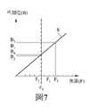
或是,參閱圖7,該比對步驟33也可利用將不同次圖案化製程量測、計算得到的該等檢測值(圖7中以B1、B2、B3表示)與由該等檢測圖案21於不同焦距(focus)下量測的間距資料計算而得之監測值與焦距作圖後得到的該標準曲線(s)進行比對、計算。Or, referring to FIG. 7 , thecomparison step 33 can also use the detection values (represented by B1 , B2 , and B3 in FIG. 7 ) obtained by measuring and calculating different patterning processes, and the values obtained from these detection values. Thedetection pattern 21 is compared and calculated by comparing and calculating the monitoring value obtained by calculating the distance data measured at different focal lengths with the standard curve (s) obtained after the focal length is plotted.

理論上,不同次之圖案化製程所產生的檢測圖案21,於相同焦距(Fs)條件下量測、計算得到的監測值(以B1、B2、B3代表由三次不同圖案化製程量測得到的監測值)應該相當,也就是說,當圖案化製程穩定時,該等監測值B1、B2、B3理應大致相同並可對應於該標準曲線(s)對應得到的監測值(Bs)以及焦距(Fs)。因此,透過該等監測值B1~B3的變化,可用於監測圖案化製程,此外,透過該等監測值B1~B3對應該標準曲線(s)的焦距值(F1、F2、F3),還可進一步得到對應之該檢測圖案21的離焦(defocus)狀況。而可進一步利用該等資訊作為圖案化製程的調整依據。Theoretically, thedetection patterns 21 generated by different patterning processes are measured and calculated under the same focal length (Fs) condition (B1 , B2 , B3 represent the amount of three different patterning processes) The measured monitoring values) should be equivalent, that is, when the patterning process is stable, the monitoring values B1 , B2 , B3 should be approximately the same and correspond to the monitoring values obtained by the standard curve (s) (Bs) and focal length (Fs). Therefore, the changes of the monitoring values B1 -B3 can be used to monitor the patterning process. In addition, the monitoring values B1 -B3 correspond to the focal length values (F1 , F2 of the standard curve (s)) , F3 ), and the corresponding defocus state of thedetection pattern 21 can be further obtained. The information can be further used as the adjustment basis of the patterning process.

此外,參閱圖8,圖8上圖是於該光罩的檢測圖案21(on mask),圖8下則是將該光罩的檢測圖案21經由圖案化製程後於該半導體基材形成對應的該等檢測圖案21(on wafer)的示意圖。由於圖案化製程的各種參數影響,所以,形成於該半導體基材上的檢測圖案21相對原始於該光罩上的檢測圖案21,會有各種尺寸或形狀的誤差產生,因此,透過利用量測實際形成於該半導體基材具有不同線路密度的檢測圖案21之間的至少兩個間距(例如:a,b或c,d)所得的監測值,還可用以監測經圖案化製程後形成於該半導體基材的該等檢測圖案21的邊緣粗糙度(line edge roughness),以及線寬粗糙度(line width roughness)。In addition, referring to FIG. 8 , the upper part of FIG. 8 is the detection pattern 21 (on mask) of the photomask, and the lower part of FIG. 8 is that thedetection pattern 21 of the photomask is formed on the semiconductor substrate after a patterning process. A schematic diagram of the detection patterns 21 (on wafer). Due to the influence of various parameters of the patterning process, the detection method formed on the semiconductor substrateThepattern 21 has various size or shape errors relative to theoriginal detection pattern 21 on the photomask. Therefore, by measuring at least two of thedetection patterns 21 actually formed on the semiconductor substrate with different line densities, The monitoring values obtained by the distances (eg: a, b or c, d) can also be used to monitor the line edge roughness of theinspection patterns 21 formed on the semiconductor substrate after the patterning process, and Line width roughness.

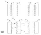
參閱圖9、10,於一些實施例中,該等檢測圖案21也可以是整合於用於不同積層對位的對位圖案單元P。如此,即可同時將用於檢測關鍵尺寸的檢測圖案單元2,與用於不同積層對對位的對位圖案單元P整合在一起形成一複合檢測圖案,而可於不同的圖案化製程過程利用該複合檢測圖案進行不同積層之間的疊對誤差檢測,並同時可監測每次圖案化製程的關鍵尺寸,而更易於監測圖案化製程的穩定性。要說明的是,圖9、10也是以在光罩的檢測圖案21及對位圖案P為例說明,然而實際量測仍是量測經圖案化製程後經成形成於半導體基板(如晶圓)上的圖案。Referring to FIGS. 9 and 10 , in some embodiments, thedetection patterns 21 may also be integrated into the alignment pattern units P used for alignment of different build-up layers. In this way, thedetection pattern unit 2 for detecting critical dimensions and the alignment pattern unit P for alignment of different layers can be integrated together to form a composite detection pattern, which can be used in different patterning processes The composite inspection pattern can detect the stacking error between different build-up layers, and can monitor the critical dimensions of each patterning process at the same time, so that it is easier to monitor the stability of the patterning process. It should be noted that, FIGS. 9 and 10 also use thedetection pattern 21 and the alignment pattern P on the photomask as examples for description, but the actual measurement is still to measure the patterning process that is formed on a semiconductor substrate (such as a wafer) ) on the pattern.

具體的說,參閱圖9,以該對位圖案單元P包含於不同次之圖案化製程形成於該半導體基材(例如晶片)的一第一對位圖案P1及一第二對位圖案P2,且該第二對位圖案P2環圍該第一對位圖案P1為例說明。Specifically, referring to FIG. 9, the alignment pattern unit P includes a first alignment pattern P1 and a second alignment pattern P2 formed on the semiconductor substrate (such as a wafer) in different order patterning processes, And the second alignment pattern P2 surrounds the first alignment pattern P1 as an example for illustration.

其中,該第一對位圖案P1具有4個於同一圖案化製程形成,成L型的第一圖案P11,且該等第一圖案P11分別位於該第一對位圖案P1所構成的正方形輪廓的四個頂角。該第二對位圖案P2環圍該第一對位圖案P1且具有正方型輪廓,也具有4個於同一圖案化製程形成,並成L型的第二圖案P21,且該等第二圖案P21也分別位於該第二對位圖案P2所構成的正方形輪廓的四個頂角。Wherein, the first alignment pattern P1 has four L-shaped first patterns P11 formed in the same patterning process, and the first patterns P11 are respectively located on the side of the square outline formed by the first alignment pattern P1 Four top corners. The second alignment pattern P2 surrounds the first alignment pattern P1 and has a square profile, and also has four L-shaped second patterns P21 formed in the same patterning process, and the second patterns P21 They are also respectively located at the four top corners of the square outline formed by the second alignment pattern P2.

當該等檢測圖案21為整合於該對位圖案單元P時,是將該第一圖案P11及第二圖案P21該視為該等檢測圖案21的該主體部211,因此,該等沿伸部212即可形成於相鄰的該兩個第一圖案P11,及/或第二圖案P21彼此相對的表面,並令該第一圖案P11及該第二圖案P21於沿同一方向,兩兩相對的表面會具有不同的圖案(如圖9所示該第一圖案P11及該第二圖案P21於沿該第一方向X及該第二方向Y間隔的兩個位置的相對表面會具有不同佈局圖案(layout)),而可於該第一方向X及該第二方向Y得到由兩種不同佈局圖案形成的間距(A、a)、(B,b)、(C,c)、(D,d)。透過互相比對形成於該晶片上的該第一圖案P11於相同方向,不同佈局圖案的兩相對表面的距離的比值(A/a)與(B/b),及/或互相比對該第二圖案21於相同方向,不同佈局圖案的兩相對表面的距離的比值(C/c)與(D/d);或是比對於同一晶片的不同位置形成的該第一圖案P11及該第二圖案P21於相同位置的距離的比值(A/a)、(B/b)、(C/c),或(D/d);或是比對於不同晶片形成,但於相同位置之距離的比值(A/a)、(B/b)、(C/c),或(D/d),即可監測各個圖案化製程產生之圖案的關鍵尺寸偏差。When thedetection patterns 21 are integrated into the alignment pattern unit P, the first pattern P11 and the second pattern P21 should be regarded as themain body portion 211 of thedetection patterns 21 . Therefore, theextended portions 212 can be formed on the surfaces of the two adjacent first patterns P11 and/or the second patterns P21 that are opposite to each other, and the first patterns P11 and the second patterns P21 are in the same direction, opposite to each other. The surfaces will have different patterns (as shown in FIG. 9 , the opposite surfaces of the first pattern P11 and the second pattern P21 at two positions spaced apart along the first direction X and the second direction Y will have different layout patterns ( layout)), and the pitches (A, a), (B, b), (C, c), (D, d) formed by two different layout patterns can be obtained in the first direction X and the second direction Y ). By comparing the ratios (A/a) and (B/b) of the distances between the two opposite surfaces of the first pattern P11 formed on the wafer in the same direction, different layout patterns, and/or comparing the first pattern P11 with each other The ratios (C/c) and (D/d) of the distances between the two opposite surfaces of the twopatterns 21 in the same direction with different layout patterns; or the ratio of the first patterns P11 andThe ratio of the distances (A/a), (B/b), (C/c), or (D/d) of the second pattern P21 at the same position; The ratio of the distances (A/a), (B/b), (C/c), or (D/d) can monitor the critical dimension deviation of the patterns produced by each patterning process.

又,參閱圖10,該等檢測圖案21也可以是整合於一箱型對位圖案(box-in-box)單元P。該箱型對位圖案(box-in-box)單元P也具有由不同圖案化製程產生的該第一對位圖案P1及第二對位圖案P2。其中,該第一對位圖案P1位於內層並具有多個成陣列(圖10以3x3表示)排列的第一圖案P11,該第二對位圖案P2位於外層並環圍該第一對位圖案P1。該等檢測圖案21可以是形成於至少其中一個第一圖案P11的表面(圖10是以該等檢測圖案21形成多個第一圖案P11表面為例說明),而與該等對位圖案單元P整合在一起,形成該複合檢測圖案。利用該複合檢測圖案也可於不同圖案化製程過程進行不同積層之間的疊對誤差檢測,並同時可監測各個圖案化製程的關鍵尺寸,而更易於監測製程的穩定性。Also, referring to FIG. 10 , thedetection patterns 21 can also be integrated into a box-in-box unit P. The box-in-box unit P also has the first alignment pattern P1 and the second alignment pattern P2 produced by different patterning processes. Wherein, the first alignment pattern P1 is located on the inner layer and has a plurality of first patterns P11 arranged in an array (represented by 3×3 in FIG. 10 ), and the second alignment pattern P2 is located on the outer layer and surrounds the first alignment pattern P1. Thedetection patterns 21 may be formed on the surface of at least one of the first patterns P11 ( FIG. 10 is an example of thedetection patterns 21 forming the surfaces of a plurality of first patterns P11 ), and the pattern units P are aligned with thedetection patterns 21 . integrated together to form the composite detection pattern. The composite detection pattern can also be used to detect the stacking error between different build-up layers in different patterning processes, and at the same time, the critical dimensions of each patterning process can be monitored, and it is easier to monitor the stability of the process.

綜上所述,本發明利用光學取像方式取得由圖案化製程形成的多個檢測圖案21,利用量測得到該等檢測圖案21所產生的至少兩個間距,利用將該至少兩個間距進行計算後,得到與該等檢測圖案21的關鍵尺寸偏移相關的監測值,因此,可透過對該等監測值的監控,例如,可利用將該等監測值得到與檢測圖案單元形成時間、量測位置,及量測晶圓片號其中至少一者相關的監測曲線,或將該等監測值與一預設值比對,或是利用將每一次圖案化製程量測計算得到的該等監測值與透過該等檢測圖案21量測計算而得的監測值-焦距(focus)標準曲線進行比對,即可得到該等不同圖案化製程的關鍵尺寸偏移檢測結果,還可進一步得到對應之該圖案化製程的離焦(defocus)狀況。此外,利用將該等檢測圖案21與用於不同積層對對位的對位圖案單元P整合在一起形成一複合檢測圖案,透過該複合檢測圖案了可檢測不同圖案化製程的積層疊對誤差檢測,並同時可監測各個圖案化製程的關鍵尺寸變異,而更易於監測製程的穩定性,故確實可達成本發明之目的。To sum up, the present invention uses optical imaging to obtain a plurality ofdetection patterns 21 formed by a patterning process, obtains at least two distances generated by thedetection patterns 21 by measurement, and uses the at least two distances to measure the at least two distances. After the calculation, the monitoring values related to the critical dimension offset of thedetection patterns 21 are obtained. Therefore, through monitoring the monitoring values, for example, the monitoring values can be used to form a unit of the detection pattern.The monitoring curve related to at least one of the time, the measurement position, and the measurement wafer number, or compare the monitoring values with a preset value, or use the measurement calculated for each patterning process. The monitoring values are compared with the monitoring value-focus standard curve measured and calculated through thedetection patterns 21, so as to obtain the critical dimension shift detection results of the different patterning processes, and further The corresponding defocus state of the patterning process is obtained. In addition, a composite detection pattern is formed by integrating thedetection patterns 21 with the alignment pattern units P used for alignment and alignment of different layers, and through the composite detection pattern, it is possible to detect the error detection of layer-by-layer alignment in different patterning processes. , and can monitor the critical dimension variation of each patterning process at the same time, and it is easier to monitor the stability of the process, so it can indeed achieve the purpose of the present invention.

惟以上所述者,僅為本發明之實施例而已,當不能以此限定本發明實施之範圍,凡是依本發明申請專利範圍及專利說明書內容所作之簡單的等效變化與修飾,皆仍屬本發明專利涵蓋之範圍內。However, the above are only examples of the present invention, and should not limit the scope of the present invention. Any simple equivalent changes and modifications made according to the scope of the application for patent of the present invention and the content of the patent specification are still within the scope of the present invention. within the scope of the invention patent.

31:量測步驟31: Measurement steps

32:計算步驟32: Calculation steps

33:比對步驟33: Comparison step

Claims (18)

Translated fromChinese
一種半導體圖案化製程的檢測方法,用於監測半導體圖案化製程,包含: 一量測步驟,重複量測於相同或不同的一半導體基材上,經由圖案化製程後產生之相同的多個檢測圖案於相同位置的至少兩個間距,該至少兩個間距是由具有不同線路密度的檢測圖案所產生,得到多組對應不同次之圖案化製程的檢測數據,且每一組檢測數據包含至少兩個間距; 一計算步驟,將每一次圖案化製程量得的檢測數據進行四則運算,得到多個對應該等不同次之圖案化製程的監測值;及 一比對步驟,利用該等監測值獲得一與該檢測圖案單元形成時間、量測位置,及量測晶圓片號其中至少一者相關的監測曲線或將該等監測值與一預設值比對,得到該等檢測圖案單元與關鍵尺寸變化相關的檢測結果。A detection method for a semiconductor patterning process, used for monitoring the semiconductor patterning process, comprising: A measuring step, repeating measurement on the same or a different semiconductor substrate, at least two spacings of the same plurality of detection patterns generated after the patterning process at the same position, the at least two spacings are formed by having different spacings The detection pattern of the line density is generated, and a plurality of sets of detection data corresponding to different patterning processes are obtained, and each set of detection data includes at least two spacings; In a calculation step, four arithmetic operations are performed on the detection data obtained in each patterning process to obtain a plurality of monitoring values corresponding to the patterning process of the same level; and a comparison step, using the monitoring values to obtain a monitoring curve related to at least one of the detection pattern unit formation time, the measurement position, and the measurement wafer number, or the monitoring values and a preset value By comparison, the detection results related to the change of the critical dimension of the detection pattern units are obtained.如請求項1所述的檢測方法,其中,該預設值是製程偏移誤差容許值,或是使用者自行定義之偏移誤差容許值。The detection method according to claim 1, wherein the preset value is a process offset error tolerance value, or a user-defined offset error tolerance value.如請求項1所述的檢測方法,其中,該計算步驟利用將該至少兩個間距進行減法或除法運算,以得到該等監測值。The detection method according to claim 1, wherein the calculation step utilizes subtraction or division of the at least two distances to obtain the monitoring values.如請求項1所述的檢測方法,其中,該至少兩個間距可分別取自相同或不同方向。The detection method according to claim 1, wherein the at least two distances can be taken from the same or different directions respectively.如請求項4所述的檢測方法,其中,該等檢測圖案至少沿一第一方向間隔排列,每一個檢測圖案具有一沿與該第一方向相交的第二方向延伸的主體部,且該等檢測圖案的其中至少一者具有一位於相應的該主體部的其中至少一表面的延伸部,該延伸部具有多個彼此間隔排列的延伸段,且該至少兩個間距是由量測具有不同線路密度之延伸部的檢測圖案而得。The detection method of claim 4, wherein the detection patterns are arranged at intervals along at least a first direction, each detection pattern has a main body portion extending along a second direction intersecting with the first direction, and the detection patterns At least one of the detection patterns has an extension portion located on at least one surface of the corresponding main body portion, the extension portion has a plurality of extension segments arranged at intervals from each other, and the at least two distances have different lines by measuring The detection pattern of the extension of the density is obtained.如請求項5所述的檢測方法,其中,該等延伸段可自相應的該主體部的至少部分表面沿該第二方向間隔排列,或自相應的主體部的至少部分表面沿該第一方向間隔排列。The detection method according to claim 5, wherein the extending segments can be spaced from at least part of the surface of the corresponding main body part along the second direction, or from at least part of the surface of the corresponding main body part in the first direction spaced.如請求項5所述的檢測方法,其中,該等檢測圖案的其中至少一者的該延伸部會同時設置於相應的主體部的兩個表面。The detection method according to claim 5, wherein the extension part of at least one of the detection patterns is simultaneously disposed on both surfaces of the corresponding main body part.如請求項5所述的檢測方法,其中,該等檢測圖案的其中至少兩個會具有自該兩個主體部相對的表面設置的延伸部,且該兩個彼此相對之延伸部的延伸段具有相同的尺寸間距。The detection method as recited in claim 5, wherein at least two of the detection patterns have extension portions disposed from opposite surfaces of the two main body portions, and the extension sections of the two opposite extension portions have same size spacing.如請求項5所述的檢測方法,其中,該等檢測圖案的其中至少兩個分別具有自該主體部相對的表面設置的延伸部,且該兩個彼此相對之延伸部成鏡像設置。The detection method according to claim 5, wherein at least two of the detection patterns respectively have extension portions provided from opposite surfaces of the main body portion, and the two mutually opposite extension portions are provided in mirror images.如請求項5所述的檢測方法,其中,該等檢測圖案的其中至少兩個分別具有自該主體部相對的表面延伸的延伸部,且每一個延伸部具有多個沿該第一方向及該第二方向間隔延伸排列而形成具有格柵結構的延伸段。The detection method of claim 5, wherein at least two of the detection patterns respectively have extension portions extending from opposite surfaces of the main body portion, and each extension portion has a plurality of extension portions along the first direction and the The second direction is extended and arranged at intervals to form extension sections having a grid structure.如請求項1或5所述的檢測方法,其中,該等檢測圖案成陣列間隔排列,每一個檢測圖案具有一主體部,該等檢測圖案的其中至少一者會具有一自相應的該主體部的其中至少一表面延伸的延伸部,該延伸部具有多個彼此間隔排列的延伸段,該等延伸段可佔滿或未佔滿該其中至少一表面。The detection method according to claim 1 or 5, wherein the detection patterns are arranged at intervals in an array, each detection pattern has a main body portion, and at least one of the detection patterns has a corresponding main body portion The extension part extends from at least one surface of the extension part, and the extension part has a plurality of extension segments arranged at intervals from each other, and the extension segments can occupy or not occupy the at least one surface.一種檢測圖案單元,供用於監測半導體圖案化製程,包含:至少兩個沿第一方向間隔排列的檢測圖案,每一個檢測圖案均具有一沿與該第一方向相交的一第二方向延伸的主體部,該等檢測圖案的其中至少一者具有一設置於相應的該主體部的其中至少一表面的延伸部,該延伸部具有多個彼此間隔排列的延伸段,且該等延伸段可佔滿未佔滿該其中至少一表面,而可令該等檢測圖案產生至少兩個由不同線路密度造成的間距。A detection pattern unit for monitoring a semiconductor patterning process, comprising: at least two detection patterns spaced along a first direction, each detection pattern having a main body extending along a second direction intersecting with the first direction part, at least one of the detection patterns has an extension part disposed on at least one surface of the corresponding main body part, the extension part has a plurality of extension sections arranged at intervals from each other, and the extension sections can be fully occupied Not filling at least one of the surfaces can make the detection patterns produce at least two spacings caused by different line densities.如請求項12所述的檢測圖案單元,其中,該等延伸段可沿該第一方向與相應的該主體部的表面間隔排列,或自相應的主體部的表面沿該第二方向間隔排列。The detection pattern unit of claim 12, wherein the extending segments can be spaced apart from the surface of the corresponding main body portion along the first direction, or spaced along the second direction from the surface of the corresponding main body portion.如請求項12所述的檢測圖案單元,其中,至少兩個檢測圖案位於同一側邊的延伸部具有不同的線路密度,該至少兩個間距是由該等具有不同線路密度的檢測圖案產生。The detection pattern unit of claim 12, wherein the extension portions of at least two detection patterns located on the same side have different line densities, and the at least two spacings are generated by the detection patterns with different line densities.如請求項12所述的檢測圖案單元,其中,該至少兩個檢測圖案具有自該兩個主體部相對的表面設置的延伸部,且該兩個彼此相對之延伸部的延伸段具有相同的尺寸間距。The detection pattern unit as claimed in claim 12, wherein the at least two detection patterns have extension portions provided from opposite surfaces of the two main body portions, and the extension sections of the two mutually opposite extension portions have the same size spacing.如請求項12所述的檢測圖案單元,其中,該等檢測圖案的其中至少兩個分別具有自該主體部相對的表面設置的延伸部,且該兩個彼此相對之延伸部成鏡像設置。The detection pattern unit of claim 12, wherein at least two of the detection patterns respectively have extension portions provided from opposite surfaces of the main body portion, and the two mutually opposite extension portions are provided in mirror images.如請求項12所述的檢測圖案單元,其中,該等檢測圖案的其中至少兩個分別具有自該主體部相對的表面延伸的延伸部,且每一個延伸部具有多個沿該第一方向及該第二方向間隔延伸排列而形成具有格柵結構的延伸段。The detection pattern unit of claim 12, wherein at least two of the detection patterns respectively have extension portions extending from opposite surfaces of the main body portion, and each extension portion has a plurality of extending portions along the first direction and The second direction is extended and arranged at intervals to form an extension section having a grid structure.如請求項12所述的檢測圖案單元,其中,該等檢測圖案成陣列間隔排列,每一個檢測圖案具有一主體部,該等檢測圖案的其中至少部分會具有一自相應的該主體部的其中至少一表面延伸的延伸部,且該延伸部具有多個彼此間隔排列的延伸段。The detection pattern unit of claim 12, wherein the detection patterns are arranged at intervals in an array, each detection pattern has a main body portion, and at least part of the detection patterns has an inner portion from the corresponding main body portion. At least one extension part extending from a surface, and the extension part has a plurality of extension segments arranged at intervals from each other.
TW110123365A2021-06-252021-06-25 Detection method and detection pattern unit of semiconductor patterning processTWI760255B (en)

Priority Applications (1)

Application NumberPriority DateFiling DateTitle
TW110123365ATWI760255B (en)2021-06-252021-06-25 Detection method and detection pattern unit of semiconductor patterning process

Applications Claiming Priority (1)

Application NumberPriority DateFiling DateTitle
TW110123365ATWI760255B (en)2021-06-252021-06-25 Detection method and detection pattern unit of semiconductor patterning process

Publications (2)

Publication NumberPublication Date
TWI760255Btrue TWI760255B (en)2022-04-01
TW202300901A TW202300901A (en)2023-01-01

Family

ID=82198737

Family Applications (1)

Application NumberTitlePriority DateFiling Date
TW110123365ATWI760255B (en)2021-06-252021-06-25 Detection method and detection pattern unit of semiconductor patterning process

Country Status (1)

CountryLink
TW (1)TWI760255B (en)

Citations (4)

* Cited by examiner, † Cited by third party
Publication numberPriority datePublication dateAssigneeTitle
TW200633104A (en)*2004-12-222006-09-16Jordan Valley SemiconductorsMeasurement of critical dimensions using X-ray diffraction in reflection mode
TW201818468A (en)*2016-11-032018-05-16聯華電子股份有限公司Structure of critical dimension bar and semiconductor thereof
TWI711900B (en)*2018-06-042020-12-01荷蘭商Asml荷蘭公司Method for improving a process model for a patterning process and related computer program product
US20210041791A1 (en)*2019-08-062021-02-11Samsung Display Co., Ltd.Method for measuring critical dimension of photoresist pattern

Patent Citations (4)

* Cited by examiner, † Cited by third party
Publication numberPriority datePublication dateAssigneeTitle
TW200633104A (en)*2004-12-222006-09-16Jordan Valley SemiconductorsMeasurement of critical dimensions using X-ray diffraction in reflection mode
TW201818468A (en)*2016-11-032018-05-16聯華電子股份有限公司Structure of critical dimension bar and semiconductor thereof
TWI711900B (en)*2018-06-042020-12-01荷蘭商Asml荷蘭公司Method for improving a process model for a patterning process and related computer program product
US20210041791A1 (en)*2019-08-062021-02-11Samsung Display Co., Ltd.Method for measuring critical dimension of photoresist pattern

Also Published As

Publication numberPublication date
TW202300901A (en)2023-01-01

Similar Documents

PublicationPublication DateTitle
TWI721281B (en)Overlay error measurement structure and the method of measuring overlay error
US10824081B2 (en)Metrology method for a semiconductor manufacturing process
US9316925B2 (en)Methods for monitoring source symmetry of photolithography systems
US8592287B2 (en)Overlay alignment mark and method of detecting overlay alignment error using the mark
US9400435B2 (en)Method of correcting overlay error
KR102467186B1 (en)Test structures and metrology technique utilizing the test structures for measuring in patterned structures
US10755016B2 (en)Hot spot and process window monitoring
TW388803B (en)A structure and method of measuring overlapping marks
US20160334208A1 (en)Overlay mark pattern and method of measuring overlay
KR101714616B1 (en)Method for measuring overlay between three layers
JP2010267931A (en) Pattern formation method and pattern design method
TWI760255B (en) Detection method and detection pattern unit of semiconductor patterning process
CN109119353A (en)Semiconductor pattern post etch monitoring overlay and critical dimension
US7754396B2 (en)Mask with focus measurement pattern and method for measuring focus value in exposure process using the same
JP2007206333A (en)Mask for measuring flare and method for measuring flare
KR20130062697A (en)Overlay vernier and the method for measuring overlay accuracy by using the same
TWI850996B (en) Monitoring pattern, detection method and detection system for semiconductor patterning process
TW202318614A (en)Detection pattern unit for a semiconductor device, and method and system for detecting a pattern on a semiconductor device using the detection pattern unit
JP2009186934A (en) Mask measuring method and mask manufacturing method
JP2023043534A (en)Measuring method, measuring apparatus, and mark
KR100866747B1 (en) Overlay vernier of semiconductor device and method of forming the same
CN115588621A (en)Offset monitoring method for front and back side graphs of wafer
KR20120067129A (en)Overlay vernier and method for measuring overlay using the same
CN118502203A (en)OVL overlay mark graph and method for improving overlay error measurement accuracy
KR20080088914A (en) Overlay vernier of semiconductor device and manufacturing method of semiconductor device

[8]ページ先頭

©2009-2025 Movatter.jp