TWI759198B - System for processing micro light emitting diode - Google Patents
System for processing micro light emitting diodeDownload PDFInfo
- Publication number
- TWI759198B TWI759198BTW110116423ATW110116423ATWI759198BTW I759198 BTWI759198 BTW I759198BTW 110116423 ATW110116423 ATW 110116423ATW 110116423 ATW110116423 ATW 110116423ATW I759198 BTWI759198 BTW I759198B
- Authority
- TW
- Taiwan
- Prior art keywords
- substrate
- projection
- switching unit
- disposed
- pixel electrode
- Prior art date
Links
Images


Classifications
- H—ELECTRICITY
- H10—SEMICONDUCTOR DEVICES; ELECTRIC SOLID-STATE DEVICES NOT OTHERWISE PROVIDED FOR
- H10H—INORGANIC LIGHT-EMITTING SEMICONDUCTOR DEVICES HAVING POTENTIAL BARRIERS
- H10H20/00—Individual inorganic light-emitting semiconductor devices having potential barriers, e.g. light-emitting diodes [LED]
- H10H20/01—Manufacture or treatment
- H10H20/011—Manufacture or treatment of bodies, e.g. forming semiconductor layers
- H10H20/018—Bonding of wafers
- G—PHYSICS
- G03—PHOTOGRAPHY; CINEMATOGRAPHY; ANALOGOUS TECHNIQUES USING WAVES OTHER THAN OPTICAL WAVES; ELECTROGRAPHY; HOLOGRAPHY
- G03F—PHOTOMECHANICAL PRODUCTION OF TEXTURED OR PATTERNED SURFACES, e.g. FOR PRINTING, FOR PROCESSING OF SEMICONDUCTOR DEVICES; MATERIALS THEREFOR; ORIGINALS THEREFOR; APPARATUS SPECIALLY ADAPTED THEREFOR
- G03F1/00—Originals for photomechanical production of textured or patterned surfaces, e.g., masks, photo-masks, reticles; Mask blanks or pellicles therefor; Containers specially adapted therefor; Preparation thereof
- H—ELECTRICITY
- H10—SEMICONDUCTOR DEVICES; ELECTRIC SOLID-STATE DEVICES NOT OTHERWISE PROVIDED FOR
- H10H—INORGANIC LIGHT-EMITTING SEMICONDUCTOR DEVICES HAVING POTENTIAL BARRIERS
- H10H20/00—Individual inorganic light-emitting semiconductor devices having potential barriers, e.g. light-emitting diodes [LED]
- H10H20/01—Manufacture or treatment
- H—ELECTRICITY
- H10—SEMICONDUCTOR DEVICES; ELECTRIC SOLID-STATE DEVICES NOT OTHERWISE PROVIDED FOR
- H10H—INORGANIC LIGHT-EMITTING SEMICONDUCTOR DEVICES HAVING POTENTIAL BARRIERS
- H10H29/00—Integrated devices, or assemblies of multiple devices, comprising at least one light-emitting semiconductor element covered by group H10H20/00
- H10H29/10—Integrated devices comprising at least one light-emitting semiconductor component covered by group H10H20/00
- H10H29/14—Integrated devices comprising at least one light-emitting semiconductor component covered by group H10H20/00 comprising multiple light-emitting semiconductor components
- H10H29/142—Two-dimensional arrangements, e.g. asymmetric LED layout
Landscapes
- Physics & Mathematics (AREA)
- General Physics & Mathematics (AREA)
- Design And Manufacture Of Integrated Circuits (AREA)
- Semiconductor Lasers (AREA)
- Liquid Crystal (AREA)
Abstract
Description
Translated fromChinese本揭示內容是關於一種供雷射光源使用的選擇性切換式光罩,且特別是關於一種用於微型發光二極體的選擇性切換式光罩。The present disclosure relates to a selectively switchable mask for use with a laser light source, and more particularly, to a selectively switchable mask for micro light emitting diodes.
隨著面板技術的持續進步,微型發光二極體(micro light emitting diode;micro LED)可應用於各種顯示器中,例如無邊框顯示器、筆記型電腦顯示器、穿戴型顯示器等。儘管micro LED具有亮度高、反應時間短、發光效能高等優點,micro LED的組裝仍面臨生產效率低和製造成本高等問題。With the continuous advancement of panel technology, micro light emitting diodes (micro LEDs) can be applied to various displays, such as borderless displays, notebook computer displays, wearable displays, and the like. Although micro LEDs have the advantages of high brightness, short response time, and high luminous efficacy, the assembly of micro LEDs still faces the problems of low production efficiency and high manufacturing costs.
鑑於上述,目前亟需發展出一種新的組裝micro LED的方法以克服前述問題。In view of the above, there is an urgent need to develop a new method for assembling micro LEDs to overcome the aforementioned problems.
本揭示內容提供了一種供雷射光源使用的選擇性切換式光罩,選擇性切換式光罩包含設置於雷射光源之下的切換單元。切換單元包含第一基板、與第一基板相對的第二基板、薄膜電晶體元件、共用電極和可切換光穿透層。像素電極設置於第一基板上。共用電極設置於第二基板上。可切換光穿透層設置於像素電極與共用電極之間。The present disclosure provides a selectively switchable photomask for a laser light source, the selectively switchable photomask includes disposed on the laser light sourcethe switching unit below. The switching unit includes a first substrate, a second substrate opposite to the first substrate, a thin film transistor element, a common electrode and a switchable light transmission layer. The pixel electrode is arranged on the first substrate. The common electrode is disposed on the second substrate. The switchable light transmission layer is disposed between the pixel electrode and the common electrode.
在一些實施方式中,可切換光穿透層為液晶層。In some embodiments, the switchable light transmissive layer is a liquid crystal layer.
在一些實施方式中,切換單元提供小於約30%的穿透率。In some embodiments, the switching unit provides a transmittance of less than about 30%.
在一些實施方式中,切換單元提供約30%至約80%的穿透率。In some embodiments, the switching unit provides a transmittance of about 30% to about 80%.
在一些實施方式中,切換單元提供約80%至約100%的穿透率。In some embodiments, the switching unit provides a transmittance of about 80% to about 100%.
在一些實施方式中,選擇性切換式光罩更包含設置於第二基板和用電極之間的遮光元件,其中遮光元件具有第一投影於第一基板上,像素電極具有第二投影於第一基板上,第一投影與第二投影交錯設置。In some embodiments, the selectively switchable photomask further includes a shading element disposed between the second substrate and the use electrode, wherein the shading element has a first projection on the first substrate, and the pixel electrode has a second projection on the first On the substrate, the first projection and the second projection are arranged alternately.
在一些實施方式中,選擇性切換式光罩更包含設置於第二基板之上的遮光元件,其中遮光元件具有第一投影於第一基板上,像素電極具有第二投影於第一基板上,第一投影與第二投影交錯設置。In some embodiments, the selectively switchable mask further includes a light shielding element disposed on the second substrate, wherein the light shielding element has a first projection on the first substrate, and the pixel electrode has a second projection on the first substrate, The first projection and the second projection are alternately arranged.
在一些實施方式中,選擇性切換式光罩更包含薄膜電晶體元件和遮光元件。薄膜電晶體元件設置於第一基板上,且與像素電極分離。遮光元件設置於該薄膜電晶體元件上,其中遮光元件具有第一投影於第一基板上,像素電極具有第二投影於第一基板上,第一投影與第二投影交錯設置。In some embodiments, the selectively switchable photomask further includes a thin film transistor element and a light shielding element. The thin film transistor element is arranged on the first substrate and is separated from the pixel electrode. The shading element is arranged on the thin film transistor element, wherein the shading element has a first projection on the first substrate,The pixel electrode has a second projection on the first substrate, and the first projection and the second projection are alternately arranged.
在一些實施方式中,可切換光穿透層為電致變色層。In some embodiments, the switchable light transmissive layer is an electrochromic layer.
在一些實施方式中,切換單元提供小於約20%的穿透率。In some embodiments, the switching unit provides a transmittance of less than about 20%.
在一些實施方式中,切換單元提供約20%至約60%的穿透率。In some embodiments, the switching unit provides a transmittance of about 20% to about 60%.
在一些實施方式中,切換單元提供約60%至約80%的穿透率。In some embodiments, the switching unit provides a transmittance of about 60% to about 80%.
本揭示內容提供了一種用於處理微型發光二極體的系統,包含選擇性切換式光罩以及設置於選擇性切換式光罩之下的載體基板。The present disclosure provides a system for processing miniature light emitting diodes including a selectively switchable mask and a carrier substrate disposed under the selectively switchable mask.
在一些實施方式中,用於處理微型發光二極體的系統更包含設置於載體基板下且與載體基板接觸的黏著層。In some embodiments, the system for processing the miniature light emitting diodes further includes an adhesive layer disposed under the carrier substrate and in contact with the carrier substrate.
在一些實施方式中,用於處理微型發光二極體的系統更包含設置於切換單元與載體基板之間的可移動式遮罩,可移動式遮罩具有彼此分離的複數個孔洞,其中像素電極具有第一投影於第一基板上,複數個孔洞的每一者具有第二投影於第一基板上,第一投影大於第二投影,且第二投影位於第一投影中。In some embodiments, the system for processing micro light emitting diodes further includes a movable mask disposed between the switching unit and the carrier substrate, the movable mask has a plurality of holes separated from each other, wherein the pixel electrodes There is a first projection on the first substrate, each of the plurality of holes has a second projection on the first substrate, the first projection is larger than the second projection, and the second projection is located in the first projection.
本揭示內容提供了一種用於處理微型發光二極體的系統,包含選擇性切換式光罩以及黏著層,黏著層設置於選擇性切換式光罩下且與選擇性切換式光罩的第一基板直接接觸。The present disclosure provides a system for processing miniature light emitting diodes, including a selectively switchable mask and an adhesive layer, the adhesive layerThe utility model is disposed under the selective switching mask and directly contacts with the first substrate of the selective switching mask.
以下將以實施方式對上述之說明做詳細的描述,並對本揭示內容之技術方案提供更進一步的解釋。The above description will be described in detail in the following embodiments, and further explanations will be provided for the technical solutions of the present disclosure.
100:選擇性切換式光罩100: Selectively switchable photomask
100A:選擇性切換式光罩100A: Selectively switchable photomask
100B:選擇性切換式光罩100B: Selectively switchable mask
100C:選擇性切換式光罩100C: Selectively switchable photomask
100D:選擇性切換式光罩100D: Selectively switchable photomask
100E:選擇性切換式光罩100E: Selectively switchable photomask
102:切換單元102: Switch unit
102a:切換單元102a: Switch unit
102b:切換單元102b: Switch unit
102c:切換單元102c: Switch unit
110:雷射光源110: Laser light source
112:雷射光112: Laser light
114:雷射光114: Laser light
120R:載體基板120R: Carrier substrate
120G:載體基板120G: carrier substrate
120B:載體基板120B: Carrier substrate
122R:黏著層122R: Adhesive layer
122G:黏著層122G: Adhesive layer
122B:黏著層122B: Adhesive layer
130R:micro LED130R: micro LED
130G:micro LED130G:micro LED
130B:micro LED130B: micro LED
140:載體基板140: carrier substrate
142:黏著層142: Adhesive layer
150:薄膜電晶體基板150: Thin film transistor substrate
510:第一基板510: First substrate
520:薄膜電晶體元件520: Thin Film Transistor Components
522:閘極522: Gate
523:第一金屬層523: first metal layer
524:閘極絕緣層524: gate insulating layer
526:通道層526: channel layer
528:源極/汲極528: source/drain
529:第二金屬層529: Second metal layer
530:鈍化膜530: Passivation film
540:像素電極540: pixel electrode
550:第二基板550: Second substrate
560:共用電極560: Common electrode
570:遮光元件570: Shading element
580:可切換光穿透層580: switchable light penetration layer
582a:液晶分子582a: Liquid crystal molecules
582b:液晶分子582b: Liquid crystal molecules
590:間隔件590: Spacer
920:控制元件920: Control elements
922:第二金屬層922: Second metal layer
924:鈍化膜924: Passivation film
926:像素電極926: Pixel electrode
930:可切換光穿透層930: switchable light penetration layer
932:電致變色膜932: Electrochromic Film
934:電解質934: Electrolyte
936:離子存儲導體膜936: Ion Storage Conductor Film
1000:可移動式遮罩1000: removable mask
1010:孔洞1010: Hole
R:區域R: area
P1:投影P1: Projection
P2:投影P2: Projection
P3:投影P3: Projection
P4:投影P4: Projection
P5:投影P5: Projection
X:方向X: direction
Z:方向Z: direction
當結合隨附圖式進行閱讀時,本揭示內容之詳細描述將能被充分地理解。應注意,根據業界標準實務,各特徵並非按比例繪製且僅用於圖示目的。事實上,出於論述清晰之目的,可任意增加或減小各特徵之尺寸。The detailed description of the present disclosure will be fully understood when read in conjunction with the accompanying drawings. It should be noted that, in accordance with standard industry practice, the features are not drawn to scale and are for illustration purposes only. In fact, the dimensions of the various features may be arbitrarily increased or decreased for clarity of discussion.
第1圖為根據本揭示內容之一些實施方式所繪示的巨量轉移裝置的剖面示意圖。FIG. 1 is a schematic cross-sectional view of a mass transfer device according to some embodiments of the present disclosure.
第2圖為根據本揭示內容之一些實施方式所繪示的雷射接合裝置的剖面示意圖。FIG. 2 is a schematic cross-sectional view of a laser bonding apparatus according to some embodiments of the present disclosure.
第3圖為根據本揭示內容之一些實施方式所繪示的巨量轉移裝置的立體示意圖。FIG. 3 is a schematic perspective view of a mass transfer device according to some embodiments of the present disclosure.
第4圖為根據本揭示內容之一些實施方式所繪示的選擇性切換式光罩的線路圖。FIG. 4 is a circuit diagram of a selectively switchable mask according to some embodiments of the present disclosure.
第5圖至第7圖為根據本揭示內容之一些實施方式所繪示的選擇性切換式光罩的剖面示意圖。5 to 7 are schematic cross-sectional views of a selectively switchable mask according to some embodiments of the present disclosure.
第8圖為根據本揭示內容之一些實施方式所繪示的選擇性切換式光罩的線路圖。FIG. 8 is a circuit diagram of a selectively switchable mask according to some embodiments of the present disclosure.
第9圖為根據本揭示內容之一些實施方式所繪示的選擇性切換式光罩的剖面示意圖。FIG. 9 is a schematic cross-sectional view of a selectively switchable mask according to some embodiments of the present disclosure.
第10A圖、第10B圖和第10C圖為根據本揭示內容之一些實施方式所繪示的巨量轉移裝置的立體示意圖。10A , 10B and 10C are schematic perspective views of a mass transfer device according to some embodiments of the present disclosure.
第11圖為根據本揭示內容之一些實施方式所繪示第10A圖的巨量轉移裝置的剖面示意圖。FIG. 11 is a schematic cross-sectional view of the mass transfer apparatus of FIG. 10A according to some embodiments of the present disclosure.
第12圖為根據本揭示內容之一些實施方式所繪示的巨量轉移裝置的立體示意圖。FIG. 12 is a schematic perspective view of a mass transfer device according to some embodiments of the present disclosure.
為了使本揭示內容之敘述更加詳盡與完備,可參照所附之圖式及以下所述各種實施例,圖式中相同之號碼代表相同或相似之元件。For a more detailed and complete description of the present disclosure, reference may be made to the accompanying drawings and the various embodiments described below, wherein the same numerals in the drawings represent the same or similar elements.
以下將以圖式揭露本揭示之複數個實施方式,為明確說明起見,許多實務上的細節將在以下敘述中一併說明。然而,應瞭解到,這些實務上的細節不應用以限制本揭示內容。也就是說,在本揭示內容的部分實施方式中,這些實務上的細節是非必要的。此外,為簡化圖式起見,一些習知慣用的結構與元件在圖式中將以簡單示意的方式繪示之。Several embodiments of the present disclosure will be disclosed in the following drawings, and for the sake of clarity, many practical details will be described together in the following description. It should be understood, however, that these practical details should not be used to limit the present disclosure. That is, in some embodiments of the present disclosure, these practical details are unnecessary. In addition, for the purpose of simplifying the drawings, some well-known structures and elements will be shown in a simple and schematic manner in the drawings.
在本文中,由「一數值至另一數值」表示的範圍,是一種避免在說明書中一一列舉該範圍中的所有數值的概要性表示方式。因此,某一特定數值範圍的記載,涵蓋該數值範圍內的任意數值以及由該數值範圍內的任意數值界定出的較小數值範圍,如同在說明書中明文寫出該任意數值和該較小數值範圍一樣。As used herein, a range represented by "one value to another value" is a general representation that avoids listing all the values in the range in the specification. Accordingly, the recitation of a particular numerical range includes any numerical value within that numerical range and a smaller numerical range delimited by any numerical value within that numerical range, as if it were expressly written in the specificationThe arbitrary value is the same as the smaller value range.
在實施方式與申請專利範圍中,除非內文中對於冠詞有所特別限定,否則「一」與「該」可泛指單一個或複數個。關於本文中所使用之「約」、「大約」或「大致」的用語一般通常係指數值之誤差或範圍約百分之二十以內,較佳地是約百分之十以內,更佳地則是約百分五之以內。In the embodiments and the scope of the patent application, unless there is a special limitation on the article in the context, "a" and "the" can generally refer to a single or plural. The terms "about", "approximately" or "approximately" as used herein are generally generally within about twenty percent, preferably within about ten percent, more preferably within about twenty percent of the error or range of the index value. is within about five percent.
微型發光二極體(micro light emitting diode;micro LED)顯示器由微型發光二極體陣列(micro LED array)所組成。一般來說,micro LED為可發出各種顏色的光(例如:紅光、綠光、藍光或其他顏色的光)之micro LED,而多個micro LED經組合和排列而形成micro LED陣列。在形成micro LED陣列的過程中包含將micro LED轉移到載體基板的巨量轉移操作以及將micro LED接合到薄膜電晶體基板的接合操作。A micro light emitting diode (micro light emitting diode; micro LED) display is composed of a micro light emitting diode array (micro LED array). Generally speaking, a micro LED is a micro LED that can emit light of various colors (eg, red light, green light, blue light or other colors), and a plurality of micro LEDs are combined and arranged to form a micro LED array. The process of forming the micro LED array includes a mass transfer operation of transferring the micro LED to a carrier substrate and a bonding operation of bonding the micro LED to a thin film transistor substrate.
本揭示內容提供一種可用於巨量轉移操作以及接合操作的選擇性切換式光罩。在進行巨量轉移操作時,將選擇性切換式光罩設置於雷射光源之下,可以將大量的micro LED轉移到載體基板上,從而提升生產效率。在進行接合操作時,將選擇性切換式光罩設置於雷射光源之下,可以將大量的micro LED接合到薄膜電晶體基板,從而提升生產效率。由於本揭示內容的選擇性切換式光罩可同時應用於巨量轉移和接合操作,因此,可以大幅降低製造成本,並進一步提升整體的生產效率。以下將詳細說明本揭示內容的選擇性切換式光罩之各種實施方式。The present disclosure provides a selectively switchable reticle that can be used for bulk transfer operations as well as bonding operations. In mass transfer operations, the selectively switchable mask is placed under the laser light source, and a large number of micro LEDs can be transferred to the carrier substrate, thereby improving production efficiency. During the bonding operation, the selectively switchable mask is placed under the laser light source, and a large number of micro LEDs can be bonded to the thin film transistor substrate, thereby improving the production efficiency. Since the selectively switchable reticle of the present disclosure can be applied to both bulk transfer and bonding operations, it is possible toIn order to greatly reduce the manufacturing cost and further improve the overall production efficiency. Various embodiments of the selectively switchable reticle of the present disclosure will be described in detail below.
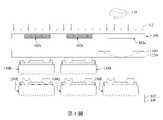
請參照第1圖,其為根據本揭示內容之一些實施方式所繪示的巨量轉移裝置的剖面示意圖。巨量轉移又可稱為選擇性雷射轉移,詳細來說,透過雷射光112選擇性地將欲轉移的micro LED轉移到載體基板上。如第1圖所示,選擇性切換式光罩100設置於提供雷射光112的雷射光源110之下,載體基板120B透過黏著層122B將micro LED 130B固定在黏著層122B上,而載體基板140透過黏著層142將micro LED 130R、130G、130B分別固定在載體基板140上。須說明的是,第1圖繪示在完成micro LED 130B的轉移之前,已先完成micro LED 130R、130G的轉移。在進行巨量轉移操作時,雷射光112通過切換單元102a和載體基板120B至黏著層122B,黏著層122B因雷射光112的能量而改變其黏著力,使得原本固定在載體基板120B的micro LED 130B脫落至載體基板140上,並藉由載體基板140上的黏著層142而固定。第1圖中micro LED 130R、130G、130B分別歷經上述的轉移操作而形成載有micro LED 130R、130G、130B的載體基板140。須說明的是,本案的micro LED 130R代表紅色的micro LED,micro LED 130G代表綠色的micro LED,micro LED 130B代表藍色的micro LED。類似地,載體基板120B和黏著層122B代表載有藍色的micro LED的載體基板和黏著層。Please refer to FIG. 1 , which is a schematic cross-sectional view of a mass transfer apparatus according to some embodiments of the present disclosure. The mass transfer can also be called selective laser transfer. In detail, the micro LED to be transferred is selectively transferred to the carrier substrate through the
在一些實施方式中,雷射光源110可為鈦藍寶石雷射器,其可具有較寬的波長調節範圍(例如約670nm至約1200nm之間的波長)。在其他實施方式中,雷射光源110可為摻有稀土元素的玻璃(SiO2)光纖作為增益介質的光纖雷射器。在一些實施方式中,雷射光112可為Nd:YAG、Nd:YVO4或Yb:YAG的固態雷射,其可提供約266nm、355nm、532nm的峰值波長(peak wavelength),但不限於此。在其他實施方式中,雷射光112可為氣態雷射,例如提供約248nm的KrF、約353nm的XeF、約193nm的ArF、約308nm的XeCl、約157nm的F2的準分子雷射;也可例如是提供約632.8nm的氦氖雷射、約1064nm的二氧化碳雷射、約6000nm至約8000nm的一氧化碳雷射、約337.1nm的氮氣雷射、約442nm的氦鎘雷射、金屬蒸氣雷射、金屬鹵化物雷射或混合氣體雷射,但不限於此。In some embodiments, the
須說明的是,選擇性切換式光罩100的切換單元102a、102b可經由調整而改變其光穿透能力。換句話說,第1圖繪示的雷射光112可穿過切換單元102a,而無法穿過切換單元102b。因此,巨量轉移又可稱為選擇性雷射轉移。此外,在一些實施方式中,巨量轉移可先將micro LED 130R選擇性地轉移至載體基板140上,再將micro LED 130G選擇性地轉移至載體基板140上,最後將micro LED130B選擇性地轉移至載體基板140上。藉由如第1圖所示的巨量轉移裝置,使得多個micro LED 130R、130G、130B經組合和排列而形成micro LED陣列。It should be noted that, the switching
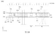
請參照第2圖,其為根據本揭示內容之一些實施方式所繪示的雷射接合裝置的剖面示意圖。詳細來說,在完成如第1圖所示之巨量轉移操作,進行如第2圖所示之雷射接合操作。將選擇性切換式光罩100設置於提供雷射光源114的雷射光源110之下,將第1圖中之載體基板140翻轉(例如轉180度),使得micro LED 130R、130G、130B朝向薄膜電晶體基板150。類似地,在進行雷射接合操作時,雷射光源114通過切換單元102a、載體基板140、黏著層142和micro LED 130R、130G、130B,使得micro LED 130R、130G、130B上的墊片(例如錫墊片)熔化並接合於薄膜電晶體基板150上。Please refer to FIG. 2 , which is a schematic cross-sectional view of a laser bonding apparatus according to some embodiments of the present disclosure. Specifically, after the mass transfer operation shown in FIG. 1 is completed, the laser bonding operation shown in FIG. 2 is performed. The selectively
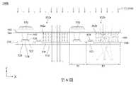
請同時參照第1圖和第3圖,第3圖為根據本揭示內容之一些實施方式所繪示的巨量轉移裝置的立體示意圖。詳細來說,第3圖為第1圖的立體示意圖。為了圖示清楚起見,第1圖中的一些元件沒有繪示於第3圖中,且第1圖中的micro LED於第3圖中繪示為簡化的長方體。Please refer to FIG. 1 and FIG. 3 simultaneously. FIG. 3 is a schematic perspective view of a mass transfer device according to some embodiments of the present disclosure. In detail, FIG. 3 is a schematic perspective view of FIG. 1 . For the sake of clarity of illustration, some elements in Fig. 1 are not shown in Fig. 3, and the micro LED in Fig. 1 is shown as a simplified cuboid in Fig. 3.
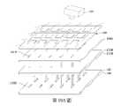
請參照第4圖,第4圖為根據本揭示內容之一些實施方式所繪示的選擇性切換式光罩100的線路圖。選擇性切換式光罩100包含以陣列排列的複數個切換單元102及佈線,其中切換單元102包含切換單元102a、102b、102c。須說明的是,本案圖式將雷射光112、114可穿過的切換單元102a繪示為沒有網點的長方體,雷射光112、114不可穿過的切換單元102b繪示為密集網點(類似黑色)的長方體,雷射光112、114可部分穿過的切換單元102c繪示為稀疏網點(類似灰色)的長方體。以下將搭配圖式詳細描述選擇性切換式光罩100的各種變化實施方式。Please refer to FIG. 4, which is one of the contents of the present disclosureA circuit diagram of the selectively
第5圖至第7圖為根據本揭示內容之一些實施方式所繪示的選擇性切換式光罩的剖面示意圖。詳細來說,第5圖至第7圖繪示第4圖的區域R的選擇性切換式光罩的剖面示意圖。區域R包含左側的切換單元102a以及右側的切換單元102b。應了解到的是,為圖式簡化起見,第4圖中的一些元件沒有繪示於第5圖至第7圖中(例如佈線)。5 to 7 are schematic cross-sectional views of a selectively switchable mask according to some embodiments of the present disclosure. In detail, FIGS. 5 to 7 are schematic cross-sectional views of the selectively switchable mask in the region R of FIG. 4 . The region R includes the
請參照第5圖,其為根據本揭示內容之一些實施方式所繪示的選擇性切換式光罩100A的剖面示意圖。選擇性切換式光罩100A包含左側的切換單元102a以及右側的切換單元102b。選擇性切換式光罩100A包含第一基板510、薄膜電晶體元件520、鈍化膜530、像素電極540、第二基板550、共用電極560、遮光元件570、可切換光穿透層580和間隔件590。第一基板510與第二基板550相對設置,且第一基板510與第二基板550之間設置有薄膜電晶體元件520、鈍化膜530、像素電極540、共用電極560、遮光元件570、可切換光穿透層580和間隔件590。Please refer to FIG. 5 , which is a schematic cross-sectional view of a selectively
如第5圖所示,薄膜電晶體元件520設置於第一基板510上,且薄膜電晶體元件520包含閘極522、源極/汲極528、通道層526以及位於通道層526和閘極522之間的閘極絕緣層524。鈍化膜530設置於薄膜電晶體元件520上。詳細來說,鈍化膜530覆蓋通道層526、源極/汲極528、閘極絕緣層524的上表面和/或側壁。閘極絕緣層524沿著第一基板510上方延伸並連續地橫跨切換單元102a和切換單元102b。鈍化膜530沿著閘極絕緣層524上方延伸並連續地橫跨切換單元102a和切換單元102b。選擇性切換式光罩100A還包含第一金屬層523和第二金屬層529。第一金屬層523與閘極522電性連接,且第二金屬層529與源極/汲極528電性連接。在一些實施方式中,閘極522和/或源極/汲極528可由鋁(Al)、銀(Ag)、銅(Cu)、鉬(Mo)、鉻(Cr)、鈦(Ti)、鉭(Ta)、或其合金所組成的單層結構。在其他實施方式中,閘極522和/或源極/汲極528可以是多層結構,例如Cu/Mo、Al/Mo、Al/Nd、Mo/W、Mo/Cu/Mo、Mo/Al/Mo、Ti/Cu/Ti、Ti/Al/Ti。在一些實施方式中,閘極522和/或源極/汲極528具有約0.3μm和約1.0μm之間的厚度(在方向X上),例如0.4、0.5、0.6、0.7、0.8、0.9μm。在一些實施方式中,通道層526可為非晶矽層或是摻雜有N型摻雜物的非晶矽層,且具有約0.1μm和約0.2μm之間的厚度,例如0.125、0.15、0.175μm。在一些實施方式中,閘極絕緣層524可由氮化矽(SiNx)或氧化矽(SiOx)所組成,且具有約0.1μm至約0.3μm之間的厚度,例如0.15、0.2、0.25μm。在一些實施方式中,鈍化膜530可由氮化矽(SiNx)所組成,且具有約0.1μm至約0.3μm之間的厚度,例如0.15、0.2、0.25μm。As shown in FIG. 5, the thin
如第5圖所示,像素電極540設置於鈍化膜530上,且每個像素電極540與對應的一個薄膜電晶體元件520相連接。共用電極560設置於第二基板550上,且沿著第二基板550上方延伸並連續地橫跨切換單元102a和切換單元102b。在一些實施方式中,像素電極540和/或共用電極560可由銦錫氧化物(indium tin oxide;ITO)或銦鋅氧化物(indium zinc oxide;IZO)所組成,且具有約0.04μm至約0.2μm之間的厚度,例如0.05、0.08、0.1、0.12、0.15、0.18μm。在一些實施方式中,像素電極540和共用電極560可具有相同的厚度,然而在其他實施方式中,像素電極540和共用電極560可具有不同的厚度。As shown in FIG. 5 , the
遮光元件570設置於第二基板550上,且位於第二基板550和共用電極560之間,其中遮光元件570具有投影P1於第一基板510上,像素電極540具有投影P2於第一基板510上,投影P1與投影P2交錯設置。詳細來說,在方向Z上,遮光元件570設置於薄膜電晶體元件520的上方,因此,當選擇性切換式光罩100A受到來自上方的雷射光112、114照射時,遮光元件570可以保護薄膜電晶體元件520以避免損壞。須說明的是,第5圖的遮光元件570繪示為涵蓋源極/汲極528的寬度,然而,更大寬度的遮光元件570也包含在本揭示內容的實施方式中,例如包含整個薄膜電晶體元件520的寬度。遮光元件570又可稱為黑色矩陣(black matrix;BM),其可以具有圖案化的矩陣,以形成類似如第4圖所示的陣列。在一些實施方式中,遮光元件570可由黑色樹脂所組成,包含樹脂、碳、光起始劑、溶劑、添加劑(例如添加劑促進劑、固化促進劑和/或表面活性劑)、或其他類似的材料,且具有約1μm至約3μm之間的厚度,例如1.5、2、2.5μm。The light-shielding
可切換光穿透層580設置於第一基板510和第二基板550之間。詳細來說,可切換光穿透層580設置於像素電極540和共用電極560之間。在一些實施方式中可切換光穿透層580為液晶層,其中液晶層包含液晶分子582a、582b。在一些實施方式中,可切換光穿透層580具有約2μm至約4μm之間的厚度,例如2.5、3、3.5μm。可藉由外部控制器(未繪示)來控制薄膜電晶體元件520的開關以及液晶層中的液晶分子582a、582b。控制薄膜電晶體元件520的開關,並對像素電極540充電而具有像素電壓(Vpixel),使得像素電壓與共用電極560的共用電壓(Vcom)間產生壓差。各個像素電極540所施加的電壓可以由對應的薄膜電晶體元件520控制,因而使得液晶層中的液晶分子582a、582b因應不同程度的壓差,而改變液晶分子582a、582b的傾倒角度,以此控制切換單元102a和切換單元102b中的穿透率。當液晶分子582a整齊排列時,雷射光112、114可以穿過液晶層,如第5圖中的切換單元102a所示。在一些實施方式中,切換單元102a提供約80%至約100%的穿透率,例如約85、90、95%的穿透率。當液晶分子582b不規則排列時,雷射光112、114無法穿過液晶層,如第5圖中的切換單元102b所示。在一些實施方式中,切換單元102b提供小於約30%的穿透率,例如約5、10、15、20、25%的穿透率。在一些實施方式中,切換單元102c提供約30%至約80%的穿透率,例如約40、50、60、70%的穿透率。在進行巨量轉移(如第1圖中之描述)時,切換單元102c可以保護micro LED 130R、130G、130B,免於受到雷射光112的能量照射而破壞micro LED 130R、130G、130B的性能。在進行雷射接合(如第2圖中之描述)時,切換單元102c可以保護薄膜電晶體基板150,免於受到雷射光114的能量照射而破壞薄膜電晶體基板150的性能。The switchable
如第5圖所示,間隔件590設置於第一基板510和第二基板550之間。詳細來說,間隔件590設置於共用電極560和鈍化膜530之間,用以提供封裝第一基板510和第二基板550時足夠的支撐力。As shown in FIG. 5 , the
請同時參照第1圖和第5圖,在一些實施方式中,當第5圖中的選擇性切換式光罩100A當作巨量轉移裝置時,雷射光112可具有約193nm、248nm、266nm、308nm、353nm、355nm或532nm的峰值波長。在一些實施方式中,雷射光源110提供約0.1mW至約10mW的功率範圍,例如0.5、1、1.5、2、3、4、5、6、7、8、9mW。在一些實施方式中,雷射光112的作用時間可為約1ms至約1fs,例如1μs、1ns、1ps。Please refer to FIGS. 1 and 5 at the same time. In some embodiments, when the selectively
請同時參照第2圖和第5圖,當第5圖中的選擇性切換式光罩100A當作雷射接合裝置時,雷射光源114可具有約980nm、1064nm或1000-1200nm的峰值波長。在一些實施方式中,雷射光源110提供約1mW至約100mW的功率範圍,例如10、20、30、40、50、60、70、80、90mW。在一些實施方式中,雷射光源114的作用時間可為約0.1ms至約1s,例如1ms、10ms、100ms。Referring to FIGS. 2 and 5 simultaneously, when the selectively
請參照第6圖,其為根據本揭示內容之一些實施方式所繪示的選擇性切換式光罩100B的剖面示意圖。第6圖的選擇性切換式光罩100B與第5圖的選擇性切換式光罩100A結構相似,差別在於遮光元件570的位置。選擇性切換式光罩100B的遮光元件570設置於第二基板550之上,且遠離第一基板510,其中遮光元件570具有投影P3於第一基板510上,像素電極540具有投影P2於第一基板510上,投影P3與投影P2交錯設置。須說明的是,第6圖中與第5圖相同或相似之元件被給予相同的符號,並省略相關說明,不再贅述。Please refer to FIG. 6 , which is a schematic cross-sectional view of a selectively
請參照第7圖,其為根據本揭示內容之一些實施方式所繪示的選擇性切換式光罩100C的剖面示意圖。第7圖的選擇性切換式光罩100C與第5圖的選擇性切換式光罩100A結構相似,差別在於遮光元件570的位置。選擇性切換式光罩100C的遮光元件570設置於薄膜電晶體元件520上,其中遮光元件570具有投影P4於第一基板510上,像素電極540具有投影P2於第一基板510上,投影P4與投影P2交錯設置。須說明的是,第7圖中與第5圖相同或相似之元件被給予相同的符號,並省略相關說明,不再贅述。Please refer to FIG. 7 , which is a schematic cross-sectional view of a selectively
請參照第8圖,其為根據本揭示內容之一些實施方式所繪示的選擇性切換式光罩100D的線路圖。選擇性切換式光罩100D包含以陣列排列的複數個切換單元102及佈線,其中切換單元102包含切換單元102a、102b、102c。須說明的是,本案圖式將雷射光112、114可穿過的切換單元102a繪示為沒有網點的長方體,雷射光112、114不可穿過的切換單元102b繪示為密集網點(類似黑色)的長方體,雷射光112、114可部分穿過的切換單元102c繪示為稀疏網點(類似灰色)的長方體。以下將搭配圖式詳細描述選擇性切換式光罩100的變化實施方式。Please refer to FIG. 8 , which is a circuit diagram of a selectively
請參照第9圖,其為根據本揭示內容之一些實施方式所繪示的選擇性切換式光罩100D的剖面示意圖。選擇性切換式光罩100D包含左側的切換單元102a以及右側的切換單元102b。選擇性切換式光罩100D包含第一基板510、控制元件920、可切換光穿透層930、第二基板550和共用電極560。第一基板510與第二基板550相對設置,且第一基板510與第二基板550之間設置有控制元件920、可切換光穿透層930和共用電極560。Please refer to FIG. 9 , which is a schematic cross-sectional view of a selectively
如第9圖所示,控制元件920設置於第一基板510上,且控制元件920包含閘極522、第一金屬層523、閘極絕緣層524、第二金屬層922、鈍化膜924、像素電極926。閘極522和第一金屬層523設置於第一基板510上,閘極絕緣層524設置於閘極522、第一金屬層523和第一基板510上,第二金屬層922設置於閘極絕緣層524上,鈍化膜924設置於第二金屬層922和閘極絕緣層524上,且像素電極926設置於鈍化膜924上。如第9圖所示,閘極絕緣層524沿著第一基板510上方延伸並連續地橫跨切換單元102a和切換單元102b,鈍化膜924沿著閘極絕緣層524上方延伸並橫跨切換單元102a和切換單元102b。須說明的是,第9圖中與第5圖相同或相似之元件被給予相同的符號,並省略相關說明,不再贅述。在一些實施方式中,第二金屬層922具有與閘極522相同或相似的特徵。在一些實施方式中,鈍化膜924具有與鈍化膜530相同或相似的特徵。像素電極926具有與像素電極540相同或相似的特徵。As shown in FIG. 9, the
請繼續參照第9圖,選擇性切換式光罩100D包含可切換光穿透層930,其中可切換光穿透層930為電致變色層。在一些實施方式中,電致變色層是選自於由WO3、MoO3、Nb2O5、TiO2、NiO、IrO2、C18Fe7N18、V2O5、Co2O3、Rh2O3、紫精、酞菁、聚噻吩類及其衍生物、紫羅精類、四硫富瓦烯、金屬酞菁類化合物、聚二氧乙烯噻吩、聚二氧乙基噻吩-聚苯乙烯磺酸複合物所組成的群組所組成。在一些實施方式中,電致變色層具有約1μm至約10μm之間的厚度,例如2、3、4、5、6、7、8、9μm。可切換光穿透層930更包含電致變色膜932、電解質934和離子存儲導體膜936。利用第二金屬層922或第一金屬層523對像素電極926提供像素電壓(Vpixel),像素電壓與共用電極560的共用電壓(Vcom)間產生壓差,使得電致變色膜932產生氧化或還原反應,以此控制切換單元102a和切換單元102b中的穿透率。在一些實施方式中,當電致變色膜932產生氧化反應時,電致變色膜932中的電致變色材料會氧化成透明的膜,因此雷射光112、114可以穿過電致變色層,如第9圖中的切換單元102a所示。在一些實施方式中,切換單元102a提供約60%至約80%的穿透率。當電致變色膜932產生還原反應時,電致變色膜932中的電致變色材料會還原成有顏色(例如藍色)的膜,因此雷射光112、114無法穿過電致變色層,如第9圖中的切換單元102b所示。須說明的是,電致變色層的變色情況會依照材料性質而有不同的變色方式,在其他實施方式中,當電致變色層產生氧化反應時會轉換成有顏色的膜,而當電致變色層產生還原反應時會轉換成透明的膜。在一些實施方式中,切換單元102a提供約60%至約80%的穿透率,例如約65、70、75%的穿透率。在一些實施方式中,切換單元102b提供小於約20%的穿透率,例如約5、10、15%的穿透率。在一些實施方式中,切換單元102c提供約20%至約60%的穿透率,例如約30、40、50%的穿透率。在進行巨量轉移(如第1圖中之描述)時,切換單元102c可以保護micro LED 130R、130G、130B,免於受到雷射光112的能量照射而破壞micro LED 130R、130G、130B的性能。在進行雷射接合(如第2圖中之描述)時,切換單元102c可以保護薄膜電晶體基板150,免於受到雷射光114的能量照射而破壞薄膜電晶體基板150的性能。Please continue to refer to FIG. 9 , the selectively
請同時參照第3圖、第5圖、第6圖、第7圖和第9圖,巨量轉移裝置更包含設置於選擇性切換式光罩100A、100B、100C、100D之下的載體基板120B以及設置於載體基板120B下的黏著層122B,其中載體基板120B與黏著層122B直接接觸。關於將micro LED 130R、130G、130B轉移到載體基板140上的詳細描述請參照第1圖的敘述。Please refer to FIG. 3 , FIG. 5 , FIG. 6 , FIG. 7 and FIG. 9 at the same time, the mass transfer apparatus further includes a
請參照第10A圖、第10B圖和第10C圖,其為根據本揭示內容之一些實施方式所繪示的巨量轉移裝置的立體示意圖。第10A圖、第10B圖和第10C圖為依據第3圖的基礎下,加入可移動式遮罩1000,其設置於選擇性切換式光罩100和載體基板120R、120G、120B之間。詳細來說,在第10A圖中,載體基板120R以及載體基板120R下的黏著層122R設置於可移動式遮罩1000之下。在第10B圖中,載體基板120G以及載體基板120G下的黏著層122G設置於可移動式遮罩1000之下。在第10C圖中,載體基板120B以及載體基板120B下的黏著層122B設置於可移動式遮罩1000之下。Please refer to FIG. 10A , FIG. 10B and FIG. 10C , which are schematic perspective views of the mass transfer device according to some embodiments of the present disclosure. FIGS. 10A , 10B and 10C are based on FIG. 3 , and a
請參照第11圖,其為根據本揭示內容之一些實施方式所繪示第10A圖的巨量轉移裝置的剖面示意圖。詳細來說,將可移動式遮罩1000設置於選擇性切換式光罩100A之下。可移動式遮罩1000具有彼此分離的複數個孔洞1010,像素電極540具有投影P2於第一基板510上,複數個孔洞1010的每一者具有投影P5於第一基板510上,投影P2大於投影P5,且投影P5位於投影P2中。須說明的是,第11圖僅示出選擇性切換式光罩100A的剖面示意圖,然而,其他選擇性切換式光罩100B、100C、100D也可置換於第11圖中,將可移動式遮罩1000分別設置於選擇性切換式光罩100B、100C、100D之下。Please refer to FIG. 11 , which is a schematic cross-sectional view of the mass transfer device of FIG. 10A according to some embodiments of the present disclosure. In detail, the
如第10A圖所示,將載體基板120R設置於可移動式遮罩1000之下,並將micro LED 130R轉移到載體基板140上。接著,移動可移動式遮罩1000,如第10B圖所示,將載體基板120G設置於可移動式遮罩1000之下,並將micro LED 130G轉移到載體基板140上。最後,再移動可移動式遮罩1000,如第10C圖所示,將載體基板120B設置於可移動式遮罩1000之下,並將micro LED 130B轉移到載體基板140上。藉由控制可移動式遮罩1000的位置分別將micro LED 130R、130G、130B轉移到載體基板140上。完成如第10A圖、第10B圖和第10C圖之巨量轉移,形成包含有micro LED 130R、130G、130B的陣列。As shown in FIG. 10A , the
在一些實施方式中,本揭示內容的選擇性切換式光罩100A、100B、100C、100D可用於巨量轉移裝置上,透過雷射光112選擇性地將欲轉移的micro LED轉移到載體基板140上,如第1圖所示。須說明的是,雷射光112可穿過的切換單元102a繪示為沒有網點,雷射光112不可穿過的切換單元102b繪示為密集網點(類似黑色),雷射光112可部分穿過的切換單元102c繪示為稀疏網點(類似灰色),其中當雷射光112不可穿過或是可部分穿過切換單元時,原本固定在載體基板120R、120G、120B的micro LED 130R、130G、130B不會脫落至載體基板140上。In some embodiments, the selectively
在其他實施方式中,本揭示內容的選擇性切換式光罩100A、100B、100C、100D可用於雷射接合操作上,透過雷射光源114選擇性地將micro LED接合並固定於薄膜電晶體基板150上,如第2圖所示。須說明的是,雷射光114可穿過的切換單元102a繪示為沒有網點,雷射光源114不可穿過的切換單元102b繪示為密集網點(類似黑色),雷射光源114可部分穿過的切換單元102c繪示為稀疏網點(類似灰色),其中當雷射光源114不可穿過或是可部分穿過切換單元時,未達micro LED 130R、130G、130B的墊片(例如錫墊片)之熔點,因此不會接合於薄膜電晶體基板150上。In other embodiments, the selectively
請參照第12圖,其為根據本揭示內容之一些實施方式所繪示的巨量轉移裝置的立體示意圖。詳細來說,選擇性切換式光罩100E更包含黏著層122R,黏著層122R設置於選擇性切換式光罩100E下且與選擇性切換式光罩100E直接接觸。更詳細來說,選擇性切換式光罩100E當作micro LED 130R的載體基板120R,micro LED 130R透過黏著層122R將micro LED 130R固定在選擇性切換式光罩100E上。在一實施方式中,選擇性切換式光罩100E上的micro LED 130R轉移到載體基板140上。在一實施方式中,選擇性切換式光罩100E上的micro LED 130G轉移到載體基板140上。在一實施方式中,選擇性切換式光罩100E上的micro LED 130B轉移到載體基板140上。關於將micro LED 130R、130G、130B轉移到載體基板140上的詳細描述請參照第1圖的敘述。Please refer to FIG. 12 , which is a three-dimensional schematic diagram of a mass transfer device according to some embodiments of the present disclosure. Specifically, the
本揭示內容的選擇性切換式光罩100E可用於巨量轉移裝置上,透過雷射光112選擇性地將欲轉移的micro LED轉移到載體基板140上,如第1圖所示。The selectively
綜上所述,本揭示內容提供了一種可用於巨量轉移操作以及接合操作的選擇性切換式光罩。在進行巨量轉移操作時,將選擇性切換式光罩設置於雷射光源之下,可以將大量的micro LED轉移到載體基板上,從而提升生產效率。在進行接合操作時,將選擇性切換式光罩設置於雷射光源之下,可以將大量的micro LED接合到薄膜電晶體基板,從而提升生產效率。由於本揭示內容的選擇性切換式光罩可同時應用於巨量轉移和接合操作,因此,可以大幅降低製造成本,並進一步提升整體的生產效率。In conclusion, the present disclosure provides a selectively switchable reticle that can be used for bulk transfer operations as well as bonding operations. In mass transfer operations, the selectively switchable mask is placed under the laser light source, and a large number of micro LEDs can be transferred to the carrier substrate, thereby improving production efficiency. During the bonding operation, the selectively switchable mask is placed under the laser light source, and a large number of micro LEDs can be bonded to the thin film transistor substrate, thereby improving the production efficiency. Since the selectively switchable photomask of the present disclosure can be applied to mass transfer and bonding operations at the same time, the manufacturing cost can be greatly reduced, and the overall production efficiency can be further improved.
對於所屬技術領域人員來說,顯而易見的是,在不脫離本揭示的範圍或精神的情況下,可以對本揭示的結構進行各種修改和變化。鑑於前述內容,本揭示意圖涵蓋落入所附申請專利範圍內的本揭示的修改和變化。It will be apparent to those skilled in the art that various modifications and variations can be made in the structures of the present disclosure without departing from the scope or spirit of the disclosure. In view of the foregoing, the present disclosure encompasses modifications and variations of the present disclosure that fall within the scope of the appended claims.
100:選擇性切換式光罩100: Selectively switchable photomask
110:雷射光源110: Laser light source
120B:載體基板120B: Carrier substrate
122B:黏著層122B: Adhesive layer
130B:micro LED130B: micro LED
140:載體基板140: carrier substrate
142:黏著層142: Adhesive layer
Claims (15)
Translated fromChinesePriority Applications (2)
| Application Number | Priority Date | Filing Date | Title |
|---|---|---|---|
| TW110116423ATWI759198B (en) | 2021-05-06 | 2021-05-06 | System for processing micro light emitting diode |
| CN202111293031.7ACN114068772B (en) | 2021-05-06 | 2021-11-03 | Selectively switchable photomask and system for processing micro light emitting diodes |
Applications Claiming Priority (1)
| Application Number | Priority Date | Filing Date | Title |
|---|---|---|---|
| TW110116423ATWI759198B (en) | 2021-05-06 | 2021-05-06 | System for processing micro light emitting diode |
Publications (2)
| Publication Number | Publication Date |
|---|---|
| TWI759198Btrue TWI759198B (en) | 2022-03-21 |
| TW202244992A TW202244992A (en) | 2022-11-16 |
Family
ID=80273622
Family Applications (1)
| Application Number | Title | Priority Date | Filing Date |
|---|---|---|---|
| TW110116423ATWI759198B (en) | 2021-05-06 | 2021-05-06 | System for processing micro light emitting diode |
Country Status (2)
| Country | Link |
|---|---|
| CN (1) | CN114068772B (en) |
| TW (1) | TWI759198B (en) |
Families Citing this family (2)
| Publication number | Priority date | Publication date | Assignee | Title |
|---|---|---|---|---|
| CN116272718A (en)* | 2022-12-30 | 2023-06-23 | 杭州联川生物技术股份有限公司 | DNA synthesizer based on TFT photomask |
| TWI829522B (en)* | 2023-02-03 | 2024-01-11 | 雷傑科技股份有限公司 | Method for die transfer |
Citations (3)
| Publication number | Priority date | Publication date | Assignee | Title |
|---|---|---|---|---|
| US20180095312A1 (en)* | 2016-10-03 | 2018-04-05 | Semiconductor Energy Laboratory Co., Ltd. | Display device, display module, and manufacturing method of display device |
| US20180203294A1 (en)* | 2017-01-16 | 2018-07-19 | Au Optronics Corporation | Pixel structure and display panel having the same |
| US20200241373A1 (en)* | 2006-08-31 | 2020-07-30 | Semiconductor Energy Laboratory Co., Ltd. | Liquid Crystal Display Device |
Family Cites Families (2)
| Publication number | Priority date | Publication date | Assignee | Title |
|---|---|---|---|---|
| CN108962789A (en)* | 2018-06-25 | 2018-12-07 | 开发晶照明(厦门)有限公司 | Micro element transfer method and micro element transfer equipment |
| KR102764899B1 (en)* | 2019-01-30 | 2025-02-12 | 삼성전자주식회사 | Micro led transfer device comprising mask and micro led transferring method using the same |
- 2021
- 2021-05-06TWTW110116423Apatent/TWI759198B/enactive
- 2021-11-03CNCN202111293031.7Apatent/CN114068772B/enactiveActive
Patent Citations (3)
| Publication number | Priority date | Publication date | Assignee | Title |
|---|---|---|---|---|
| US20200241373A1 (en)* | 2006-08-31 | 2020-07-30 | Semiconductor Energy Laboratory Co., Ltd. | Liquid Crystal Display Device |
| US20180095312A1 (en)* | 2016-10-03 | 2018-04-05 | Semiconductor Energy Laboratory Co., Ltd. | Display device, display module, and manufacturing method of display device |
| US20180203294A1 (en)* | 2017-01-16 | 2018-07-19 | Au Optronics Corporation | Pixel structure and display panel having the same |
Also Published As
| Publication number | Publication date |
|---|---|
| TW202244992A (en) | 2022-11-16 |
| CN114068772A (en) | 2022-02-18 |
| CN114068772B (en) | 2023-06-02 |
Similar Documents
| Publication | Publication Date | Title |
|---|---|---|
| JP6953646B2 (en) | Display device | |
| JP6613003B2 (en) | Liquid crystal display | |
| KR101287478B1 (en) | Display device having oxide thin film transistor and method of fabricating thereof | |
| JP5148912B2 (en) | Liquid crystal display device, semiconductor device, and electronic device | |
| KR100865244B1 (en) | Semiconductor device and manufacturing method thereof | |
| KR100707544B1 (en) | Organic electroluminescence display device | |
| TWI759198B (en) | System for processing micro light emitting diode | |
| KR20010078229A (en) | Semiconductor device and manufacturing method thereof | |
| JP2004310027A (en) | Liquid crystal display device and method of manufacturing the same | |
| JP5386547B2 (en) | Method for manufacturing semiconductor device | |
| WO2015106545A1 (en) | Method for manufacturing thin film layer pattern, display substrate, method for manufacturing display substrate, and display device | |
| KR20120007764A (en) | Array substrate including thin film transistor using micro polysilicon and manufacturing method thereof | |
| JP4831961B2 (en) | Manufacturing method and selection method of semiconductor device | |
| KR20040057714A (en) | Method for making a black matrix and liquid crystal display device using this |