TWI757450B - Method for manufacturing electrically conductive structures on a carrier material - Google Patents
Method for manufacturing electrically conductive structures on a carrier materialDownload PDFInfo
- Publication number
- TWI757450B TWI757450BTW107109229ATW107109229ATWI757450BTW I757450 BTWI757450 BTW I757450BTW 107109229 ATW107109229 ATW 107109229ATW 107109229 ATW107109229 ATW 107109229ATW I757450 BTWI757450 BTW I757450B
- Authority
- TW
- Taiwan
- Prior art keywords
- acid
- conductive
- carrier material
- metal
- iron
- Prior art date
Links
- 239000012876carrier materialSubstances0.000titleclaimsabstractdescription56
- 238000000034methodMethods0.000titleclaimsabstractdescription54
- 238000004519manufacturing processMethods0.000titleclaimsabstractdescription38
- 150000001875compoundsChemical class0.000claimsabstractdescription42
- 229910001463metal phosphateInorganic materials0.000claimsabstractdescription35
- 239000003381stabilizerSubstances0.000claimsabstractdescription30
- 239000000463materialSubstances0.000claimsdescription39
- XLYOFNOQVPJJNP-UHFFFAOYSA-NwaterSubstancesOXLYOFNOQVPJJNP-UHFFFAOYSA-N0.000claimsdescription36
- -1Phosphorus oxoacidsChemical class0.000claimsdescription31
- 229910052751metalInorganic materials0.000claimsdescription31
- 239000002184metalSubstances0.000claimsdescription31
- XEEYBQQBJWHFJM-UHFFFAOYSA-NironSubstances[Fe]XEEYBQQBJWHFJM-UHFFFAOYSA-N0.000claimsdescription26
- 239000002253acidSubstances0.000claimsdescription23
- 239000002966varnishSubstances0.000claimsdescription23
- 239000013078crystalSubstances0.000claimsdescription22
- 239000000203mixtureSubstances0.000claimsdescription19
- NBIIXXVUZAFLBC-UHFFFAOYSA-NPhosphoric acidChemical compoundOP(O)(O)=ONBIIXXVUZAFLBC-UHFFFAOYSA-N0.000claimsdescription16
- 239000002841Lewis acidSubstances0.000claimsdescription12
- 150000007513acidsChemical class0.000claimsdescription12
- 150000007517lewis acidsChemical class0.000claimsdescription12
- ABLZXFCXXLZCGV-UHFFFAOYSA-NPhosphorous acidChemical compoundOP(O)=OABLZXFCXXLZCGV-UHFFFAOYSA-N0.000claimsdescription11
- 150000003839saltsChemical class0.000claimsdescription11
- 239000010949copperSubstances0.000claimsdescription10
- CWYNVVGOOAEACU-UHFFFAOYSA-NFe2+Chemical compound[Fe+2]CWYNVVGOOAEACU-UHFFFAOYSA-N0.000claimsdescription9
- 229910000147aluminium phosphateInorganic materials0.000claimsdescription9
- 239000011777magnesiumSubstances0.000claimsdescription8
- 150000003013phosphoric acid derivativesChemical class0.000claimsdescription8
- SDEKDNPYZOERBP-UHFFFAOYSA-Hiron(ii) phosphateChemical compound[Fe+2].[Fe+2].[Fe+2].[O-]P([O-])([O-])=O.[O-]P([O-])([O-])=OSDEKDNPYZOERBP-UHFFFAOYSA-H0.000claimsdescription7
- BPLYVSYSBPLDOA-GYOJGHLZSA-Nn-[(2r,3r)-1,3-dihydroxyoctadecan-2-yl]tetracosanamideChemical compoundCCCCCCCCCCCCCCCCCCCCCCCC(=O)N[C@H](CO)[C@H](O)CCCCCCCCCCCCCCCBPLYVSYSBPLDOA-GYOJGHLZSA-N0.000claimsdescription7
- QTBSBXVTEAMEQO-UHFFFAOYSA-NAcetic acidChemical compoundCC(O)=OQTBSBXVTEAMEQO-UHFFFAOYSA-N0.000claimsdescription6
- WSFSSNUMVMOOMR-UHFFFAOYSA-NFormaldehydeChemical compoundO=CWSFSSNUMVMOOMR-UHFFFAOYSA-N0.000claimsdescription6
- MUBZPKHOEPUJKR-UHFFFAOYSA-NOxalic acidChemical compoundOC(=O)C(O)=OMUBZPKHOEPUJKR-UHFFFAOYSA-N0.000claimsdescription6
- 239000004952PolyamideSubstances0.000claimsdescription6
- RBLGLDWTCZMLRW-UHFFFAOYSA-Kdicalcium phosphate dihydrateSubstancesO.O.[Ca+2].[Ca+2].[O-]P([O-])([O-])=ORBLGLDWTCZMLRW-UHFFFAOYSA-K0.000claimsdescription6
- 150000002739metalsChemical class0.000claimsdescription6
- 229920002647polyamidePolymers0.000claimsdescription6
- 229920001169thermoplasticPolymers0.000claimsdescription6
- 229910052698phosphorusInorganic materials0.000claimsdescription5
- 239000011574phosphorusSubstances0.000claimsdescription5
- 229920001296polysiloxanePolymers0.000claimsdescription5
- KRHYYFGTRYWZRS-UHFFFAOYSA-NFluoraneChemical compoundFKRHYYFGTRYWZRS-UHFFFAOYSA-N0.000claimsdescription4
- 239000004698PolyethyleneSubstances0.000claimsdescription4
- 239000004743PolypropyleneSubstances0.000claimsdescription4
- QAOWNCQODCNURD-UHFFFAOYSA-NSulfuric acidChemical compoundOS(O)(=O)=OQAOWNCQODCNURD-UHFFFAOYSA-N0.000claimsdescription4
- 229920002877acrylic styrene acrylonitrilePolymers0.000claimsdescription4
- 125000001931aliphatic groupChemical group0.000claimsdescription4
- ZQKXOSJYJMDROL-UHFFFAOYSA-Haluminum;trisodium;diphosphateChemical compound[Na+].[Na+].[Na+].[Al+3].[O-]P([O-])([O-])=O.[O-]P([O-])([O-])=OZQKXOSJYJMDROL-UHFFFAOYSA-H0.000claimsdescription4
- WPYMKLBDIGXBTP-UHFFFAOYSA-Nbenzoic acidChemical compoundOC(=O)C1=CC=CC=C1WPYMKLBDIGXBTP-UHFFFAOYSA-N0.000claimsdescription4
- 239000003638chemical reducing agentSubstances0.000claimsdescription4
- WCMHCPWEQCWRSR-UHFFFAOYSA-Jdicopper;hydroxide;phosphateChemical compound[OH-].[Cu+2].[Cu+2].[O-]P([O-])([O-])=OWCMHCPWEQCWRSR-UHFFFAOYSA-J0.000claimsdescription4
- XPPKVPWEQAFLFU-UHFFFAOYSA-Ndiphosphoric acidChemical compoundOP(O)(=O)OP(O)(O)=OXPPKVPWEQAFLFU-UHFFFAOYSA-N0.000claimsdescription4
- 229910052749magnesiumInorganic materials0.000claimsdescription4
- 229910044991metal oxideInorganic materials0.000claimsdescription4
- 150000004706metal oxidesChemical class0.000claimsdescription4
- BDAGIHXWWSANSR-UHFFFAOYSA-Nmethanoic acidNatural productsOC=OBDAGIHXWWSANSR-UHFFFAOYSA-N0.000claimsdescription4
- NBIIXXVUZAFLBC-UHFFFAOYSA-KphosphateChemical compound[O-]P([O-])([O-])=ONBIIXXVUZAFLBC-UHFFFAOYSA-K0.000claimsdescription4
- XNGIFLGASWRNHJ-UHFFFAOYSA-Nphthalic acidChemical compoundOC(=O)C1=CC=CC=C1C(O)=OXNGIFLGASWRNHJ-UHFFFAOYSA-N0.000claimsdescription4
- 229920002037poly(vinyl butyral) polymerPolymers0.000claimsdescription4
- 229920000573polyethylenePolymers0.000claimsdescription4
- 229920000139polyethylene terephthalatePolymers0.000claimsdescription4
- 239000005020polyethylene terephthalateSubstances0.000claimsdescription4
- 229920006324polyoxymethylenePolymers0.000claimsdescription4
- 229920001155polypropylenePolymers0.000claimsdescription4
- 238000006722reduction reactionMethods0.000claimsdescription4
- 239000011734sodiumSubstances0.000claimsdescription4
- 229910019142PO4Inorganic materials0.000claimsdescription3
- 239000003822epoxy resinSubstances0.000claimsdescription3
- 239000000025natural resinSubstances0.000claimsdescription3
- 230000003647oxidationEffects0.000claimsdescription3
- 238000007254oxidation reactionMethods0.000claimsdescription3
- 235000021317phosphateNutrition0.000claimsdescription3
- 229920000647polyepoxidePolymers0.000claimsdescription3
- 229920000642polymerPolymers0.000claimsdescription3
- 229920000193polymethacrylatePolymers0.000claimsdescription3
- 229920005989resinPolymers0.000claimsdescription3
- 239000011347resinSubstances0.000claimsdescription3
- RMAQACBXLXPBSY-UHFFFAOYSA-Nsilicic acidChemical compoundO[Si](O)(O)ORMAQACBXLXPBSY-UHFFFAOYSA-N0.000claimsdescription3
- 235000012239silicon dioxideNutrition0.000claimsdescription3
- 229920001187thermosetting polymerPolymers0.000claimsdescription3
- 238000012546transferMethods0.000claimsdescription3
- KXGFMDJXCMQABM-UHFFFAOYSA-N2-methoxy-6-methylphenolChemical compound[CH]OC1=CC=CC([CH])=C1OKXGFMDJXCMQABM-UHFFFAOYSA-N0.000claimsdescription2
- OSWFIVFLDKOXQC-UHFFFAOYSA-N4-(3-methoxyphenyl)anilineChemical compoundCOC1=CC=CC(C=2C=CC(N)=CC=2)=C1OSWFIVFLDKOXQC-UHFFFAOYSA-N0.000claimsdescription2
- 239000005711Benzoic acidSubstances0.000claimsdescription2
- LSNNMFCWUKXFEE-UHFFFAOYSA-MBisulfiteChemical compoundOS([O-])=OLSNNMFCWUKXFEE-UHFFFAOYSA-M0.000claimsdescription2
- 239000004132Calcium polyphosphateSubstances0.000claimsdescription2
- FYYHWMGAXLPEAU-UHFFFAOYSA-NMagnesiumChemical compound[Mg]FYYHWMGAXLPEAU-UHFFFAOYSA-N0.000claimsdescription2
- 239000004640Melamine resinSubstances0.000claimsdescription2
- 229920000877Melamine resinPolymers0.000claimsdescription2
- GRYLNZFGIOXLOG-UHFFFAOYSA-NNitric acidChemical compoundO[N+]([O-])=OGRYLNZFGIOXLOG-UHFFFAOYSA-N0.000claimsdescription2
- 229930040373ParaformaldehydeNatural products0.000claimsdescription2
- 229930182556PolyacetalNatural products0.000claimsdescription2
- 239000004721Polyphenylene oxideSubstances0.000claimsdescription2
- 229920000388PolyphosphatePolymers0.000claimsdescription2
- 239000004793PolystyreneSubstances0.000claimsdescription2
- 229920002396PolyureaPolymers0.000claimsdescription2
- 239000004433Thermoplastic polyurethaneSubstances0.000claimsdescription2
- DHKHKXVYLBGOIT-UHFFFAOYSA-Nacetaldehyde Diethyl AcetalNatural productsCCOC(C)OCCDHKHKXVYLBGOIT-UHFFFAOYSA-N0.000claimsdescription2
- 235000011054acetic acidNutrition0.000claimsdescription2
- 125000005234alkyl aluminium groupChemical group0.000claimsdescription2
- WNROFYMDJYEPJX-UHFFFAOYSA-Kaluminium hydroxideChemical compound[OH-].[OH-].[OH-].[Al+3]WNROFYMDJYEPJX-UHFFFAOYSA-K0.000claimsdescription2
- 235000010233benzoic acidNutrition0.000claimsdescription2
- 229910000085boraneInorganic materials0.000claimsdescription2
- KGBXLFKZBHKPEV-UHFFFAOYSA-Nboric acidChemical compoundOB(O)OKGBXLFKZBHKPEV-UHFFFAOYSA-N0.000claimsdescription2
- 239000004327boric acidSubstances0.000claimsdescription2
- 229910052792caesiumInorganic materials0.000claimsdescription2
- 229910052791calciumInorganic materials0.000claimsdescription2
- 239000011575calciumSubstances0.000claimsdescription2
- 235000019827calcium polyphosphateNutrition0.000claimsdescription2
- 239000000919ceramicSubstances0.000claimsdescription2
- 229920001577copolymerPolymers0.000claimsdescription2
- 230000002950deficientEffects0.000claimsdescription2
- 229920001971elastomerPolymers0.000claimsdescription2
- 239000000806elastomerSubstances0.000claimsdescription2
- 235000019253formic acidNutrition0.000claimsdescription2
- 239000011521glassSubstances0.000claimsdescription2
- 229910052747lanthanoidInorganic materials0.000claimsdescription2
- 150000002602lanthanoidsChemical class0.000claimsdescription2
- 229910052744lithiumInorganic materials0.000claimsdescription2
- 229910017604nitric acidInorganic materials0.000claimsdescription2
- 235000006408oxalic acidNutrition0.000claimsdescription2
- 229920001568phenolic resinPolymers0.000claimsdescription2
- 239000005011phenolic resinSubstances0.000claimsdescription2
- 229920001643poly(ether ketone)Polymers0.000claimsdescription2
- 229920000747poly(lactic acid)Polymers0.000claimsdescription2
- 239000004417polycarbonateSubstances0.000claimsdescription2
- 229920000515polycarbonatePolymers0.000claimsdescription2
- 229920000728polyesterPolymers0.000claimsdescription2
- 229920000570polyetherPolymers0.000claimsdescription2
- 239000004626polylactic acidSubstances0.000claimsdescription2
- 229920001955polyphenylene etherPolymers0.000claimsdescription2
- 239000001205polyphosphateSubstances0.000claimsdescription2
- 235000011176polyphosphatesNutrition0.000claimsdescription2
- 229920000137polyphosphoric acidPolymers0.000claimsdescription2
- 229920002223polystyrenePolymers0.000claimsdescription2
- 229920001343polytetrafluoroethylenePolymers0.000claimsdescription2
- 239000004810polytetrafluoroethyleneSubstances0.000claimsdescription2
- 239000004800polyvinyl chlorideSubstances0.000claimsdescription2
- 229920000915polyvinyl chloridePolymers0.000claimsdescription2
- 229910052700potassiumInorganic materials0.000claimsdescription2
- QMRNDFMLWNAFQR-UHFFFAOYSA-Nprop-2-enenitrile;prop-2-enoic acid;styreneChemical compoundC=CC#N.OC(=O)C=C.C=CC1=CC=CC=C1QMRNDFMLWNAFQR-UHFFFAOYSA-N0.000claimsdescription2
- 229910052701rubidiumInorganic materials0.000claimsdescription2
- 229910052708sodiumInorganic materials0.000claimsdescription2
- 229910052712strontiumInorganic materials0.000claimsdescription2
- 229920003002synthetic resinPolymers0.000claimsdescription2
- 239000000057synthetic resinSubstances0.000claimsdescription2
- 229920002803thermoplastic polyurethanePolymers0.000claimsdescription2
- 229910052723transition metalInorganic materials0.000claimsdescription2
- 150000003624transition metalsChemical class0.000claimsdescription2
- UORVGPXVDQYIDP-UHFFFAOYSA-NtrihydridoboronSubstancesBUORVGPXVDQYIDP-UHFFFAOYSA-N0.000claimsdescription2
- 229920002554vinyl polymerPolymers0.000claimsdescription2
- FUFJGUQYACFECW-UHFFFAOYSA-Lcalcium hydrogenphosphateChemical compound[Ca+2].OP([O-])([O-])=OFUFJGUQYACFECW-UHFFFAOYSA-L0.000claims2
- 230000008021depositionEffects0.000claims2
- 229920001707polybutylene terephthalatePolymers0.000claims2
- 125000002777acetyl groupChemical class[H]C([H])([H])C(*)=O0.000claims1
- NIXOWILDQLNWCW-UHFFFAOYSA-Nacrylic acid groupChemical groupC(C=C)(=O)ONIXOWILDQLNWCW-UHFFFAOYSA-N0.000claims1
- FJPWFOXSXUFQQO-UHFFFAOYSA-Kaluminum;calcium;magnesium;phosphateChemical compound[Mg+2].[Al+3].[Ca+2].[O-]P([O-])([O-])=OFJPWFOXSXUFQQO-UHFFFAOYSA-K0.000claims1
- 150000001412aminesChemical class0.000claims1
- MTAZNLWOLGHBHU-UHFFFAOYSA-Nbutadiene-styrene rubberChemical compoundC=CC=C.C=CC1=CC=CC=C1MTAZNLWOLGHBHU-UHFFFAOYSA-N0.000claims1
- YYRMJZQKEFZXMX-UHFFFAOYSA-Lcalcium bis(dihydrogenphosphate)Chemical compound[Ca+2].OP(O)([O-])=O.OP(O)([O-])=OYYRMJZQKEFZXMX-UHFFFAOYSA-L0.000claims1
- 239000001506calcium phosphateSubstances0.000claims1
- 235000011180diphosphatesNutrition0.000claims1
- 235000001055magnesiumNutrition0.000claims1
- 125000005341metaphosphate groupChemical group0.000claims1
- 229910000150monocalcium phosphateInorganic materials0.000claims1
- 235000019691monocalcium phosphateNutrition0.000claims1
- 230000037361pathwayEffects0.000abstractdescription2
- 239000000047productSubstances0.000description32
- 238000002441X-ray diffractionMethods0.000description28
- 238000001465metallisationMethods0.000description14
- 238000012545processingMethods0.000description14
- 229910021519iron(III) oxide-hydroxideInorganic materials0.000description13
- 229910001385heavy metalInorganic materials0.000description12
- 239000004020conductorSubstances0.000description11
- 239000008187granular materialSubstances0.000description10
- 239000002904solventSubstances0.000description10
- KWYUFKZDYYNOTN-UHFFFAOYSA-MPotassium hydroxideChemical compound[OH-].[K+]KWYUFKZDYYNOTN-UHFFFAOYSA-M0.000description9
- 230000008901benefitEffects0.000description8
- 229910052802copperInorganic materials0.000description8
- 238000005469granulationMethods0.000description8
- 230000003179granulationEffects0.000description8
- 239000007921spraySubstances0.000description8
- 239000000126substanceSubstances0.000description8
- 150000004696coordination complexChemical class0.000description7
- IEECXTSVVFWGSE-UHFFFAOYSA-Miron(3+);oxygen(2-);hydroxideChemical compound[OH-].[O-2].[Fe+3]IEECXTSVVFWGSE-UHFFFAOYSA-M0.000description7
- BMTOKWDUYJKSCN-UHFFFAOYSA-Kiron(3+);phosphate;dihydrateChemical compoundO.O.[Fe+3].[O-]P([O-])([O-])=OBMTOKWDUYJKSCN-UHFFFAOYSA-K0.000description7
- 229910000462iron(III) oxide hydroxideInorganic materials0.000description7
- 239000000725suspensionSubstances0.000description7
- 239000004594Masterbatch (MB)Substances0.000description6
- 238000001125extrusionMethods0.000description6
- AEIXRCIKZIZYPM-UHFFFAOYSA-Mhydroxy(oxo)ironChemical compound[O][Fe]OAEIXRCIKZIZYPM-UHFFFAOYSA-M0.000description6
- 239000002245particleSubstances0.000description6
- 230000002110toxicologic effectEffects0.000description6
- 231100000027toxicologyToxicity0.000description6
- 239000011701zincSubstances0.000description6
- RYGMFSIKBFXOCR-UHFFFAOYSA-NCopperChemical compound[Cu]RYGMFSIKBFXOCR-UHFFFAOYSA-N0.000description5
- 239000000654additiveSubstances0.000description5
- 239000000853adhesiveSubstances0.000description5
- 230000001070adhesive effectEffects0.000description5
- 238000006243chemical reactionMethods0.000description5
- 229920003023plasticPolymers0.000description5
- 239000004033plasticSubstances0.000description5
- UQSXHKLRYXJYBZ-UHFFFAOYSA-NIron oxideChemical compound[Fe]=OUQSXHKLRYXJYBZ-UHFFFAOYSA-N0.000description4
- XLOMVQKBTHCTTD-UHFFFAOYSA-NZinc monoxideChemical compound[Zn]=OXLOMVQKBTHCTTD-UHFFFAOYSA-N0.000description4
- 230000000996additive effectEffects0.000description4
- VSCWAEJMTAWNJL-UHFFFAOYSA-Kaluminium trichlorideChemical compoundCl[Al](Cl)ClVSCWAEJMTAWNJL-UHFFFAOYSA-K0.000description4
- 230000004907fluxEffects0.000description4
- 239000000843powderSubstances0.000description4
- 230000008569processEffects0.000description4
- 230000005855radiationEffects0.000description4
- 230000002829reductive effectEffects0.000description4
- 239000004416thermosoftening plasticSubstances0.000description4
- ZMXDDKWLCZADIW-UHFFFAOYSA-NN,N-DimethylformamideChemical compoundCN(C)C=OZMXDDKWLCZADIW-UHFFFAOYSA-N0.000description3
- OAICVXFJPJFONN-UHFFFAOYSA-NPhosphorusChemical compound[P]OAICVXFJPJFONN-UHFFFAOYSA-N0.000description3
- GWEVSGVZZGPLCZ-UHFFFAOYSA-NTitan oxideChemical compoundO=[Ti]=OGWEVSGVZZGPLCZ-UHFFFAOYSA-N0.000description3
- 229920006097Ultramide®Polymers0.000description3
- 230000002411adverseEffects0.000description3
- 230000015572biosynthetic processEffects0.000description3
- WTEOIRVLGSZEPR-UHFFFAOYSA-Nboron trifluorideChemical compoundFB(F)FWTEOIRVLGSZEPR-UHFFFAOYSA-N0.000description3
- 238000000354decomposition reactionMethods0.000description3
- 238000006731degradation reactionMethods0.000description3
- 229910052737goldInorganic materials0.000description3
- 239000010931goldSubstances0.000description3
- 238000001746injection mouldingMethods0.000description3
- ATEAWHILRRXHPW-UHFFFAOYSA-Jiron(2+);phosphonato phosphateChemical compound[Fe+2].[Fe+2].[O-]P([O-])(=O)OP([O-])([O-])=OATEAWHILRRXHPW-UHFFFAOYSA-J0.000description3
- 229910000155iron(II) phosphateInorganic materials0.000description3
- 239000011572manganeseSubstances0.000description3
- PXHVJJICTQNCMI-UHFFFAOYSA-NnickelSubstances[Ni]PXHVJJICTQNCMI-UHFFFAOYSA-N0.000description3
- 239000003921oilSubstances0.000description3
- 239000003973paintSubstances0.000description3
- 239000002243precursorSubstances0.000description3
- 238000007639printingMethods0.000description3
- 229910052709silverInorganic materials0.000description3
- 229910015900BF3Inorganic materials0.000description2
- KAKZBPTYRLMSJV-UHFFFAOYSA-NButadieneChemical compoundC=CC=CKAKZBPTYRLMSJV-UHFFFAOYSA-N0.000description2
- 235000008733Citrus aurantifoliaNutrition0.000description2
- 229920007019PC/ABSPolymers0.000description2
- 235000011941Tilia x europaeaNutrition0.000description2
- 238000010521absorption reactionMethods0.000description2
- 239000000370acceptorSubstances0.000description2
- 229910052782aluminiumInorganic materials0.000description2
- 239000002585baseSubstances0.000description2
- ZBZJARSYCHAEND-UHFFFAOYSA-Lcalcium;dihydrogen phosphate;hydrateChemical compoundO.[Ca+2].OP(O)([O-])=O.OP(O)([O-])=OZBZJARSYCHAEND-UHFFFAOYSA-L0.000description2
- 230000015556catabolic processEffects0.000description2
- 229920001940conductive polymerPolymers0.000description2
- 238000002845discolorationMethods0.000description2
- CSVGEMRSDNSWRF-UHFFFAOYSA-Ldisodium;dihydrogen phosphateChemical compound[Na+].[Na+].OP(O)([O-])=O.OP(O)([O-])=OCSVGEMRSDNSWRF-UHFFFAOYSA-L0.000description2
- 238000001035dryingMethods0.000description2
- 230000000694effectsEffects0.000description2
- 230000005670electromagnetic radiationEffects0.000description2
- 238000000921elemental analysisMethods0.000description2
- 230000002349favourable effectEffects0.000description2
- 229910052742ironInorganic materials0.000description2
- 239000004571limeSubstances0.000description2
- 239000007788liquidSubstances0.000description2
- 238000002844meltingMethods0.000description2
- 230000008018meltingEffects0.000description2
- 150000002736metal compoundsChemical class0.000description2
- 229910052759nickelInorganic materials0.000description2
- 230000006911nucleationEffects0.000description2
- 238000010899nucleationMethods0.000description2
- 229910052763palladiumInorganic materials0.000description2
- 230000008092positive effectEffects0.000description2
- 238000002360preparation methodMethods0.000description2
- 238000010517secondary reactionMethods0.000description2
- 239000004065semiconductorSubstances0.000description2
- 238000000926separation methodMethods0.000description2
- 239000010944silver (metal)Substances0.000description2
- 229910052718tinInorganic materials0.000description2
- 239000011135tinSubstances0.000description2
- 229910052719titaniumInorganic materials0.000description2
- 239000010936titaniumSubstances0.000description2
- 150000003623transition metal compoundsChemical class0.000description2
- 238000011282treatmentMethods0.000description2
- 229910052725zincInorganic materials0.000description2
- VZSRBBMJRBPUNF-UHFFFAOYSA-N2-(2,3-dihydro-1H-inden-2-ylamino)-N-[3-oxo-3-(2,4,6,7-tetrahydrotriazolo[4,5-c]pyridin-5-yl)propyl]pyrimidine-5-carboxamideChemical compoundC1C(CC2=CC=CC=C12)NC1=NC=C(C=N1)C(=O)NCCC(N1CC2=C(CC1)NN=N2)=OVZSRBBMJRBPUNF-UHFFFAOYSA-N0.000description1
- 239000004925Acrylic resinSubstances0.000description1
- 229920000178Acrylic resinPolymers0.000description1
- OKTJSMMVPCPJKN-UHFFFAOYSA-NCarbonChemical compound[C]OKTJSMMVPCPJKN-UHFFFAOYSA-N0.000description1
- VGGSQFUCUMXWEO-UHFFFAOYSA-NEtheneChemical compoundC=CVGGSQFUCUMXWEO-UHFFFAOYSA-N0.000description1
- 229920000084Gum arabicPolymers0.000description1
- 229910021577Iron(II) chlorideInorganic materials0.000description1
- 239000002879Lewis baseSubstances0.000description1
- 101100513612Microdochium nivale MnCO geneProteins0.000description1
- 239000000020NitrocelluloseSubstances0.000description1
- IRUGTMYLJLCWPR-UHFFFAOYSA-KP(=O)([O-])([O-])[O-].[Mg+].[Fe+2]Chemical compoundP(=O)([O-])([O-])[O-].[Mg+].[Fe+2]IRUGTMYLJLCWPR-UHFFFAOYSA-K0.000description1
- 239000004972Polyurethane varnishSubstances0.000description1
- 241000978776Senegalia senegalSpecies0.000description1
- 229910003910SiCl4Inorganic materials0.000description1
- BQCADISMDOOEFD-UHFFFAOYSA-NSilverChemical compound[Ag]BQCADISMDOOEFD-UHFFFAOYSA-N0.000description1
- FJWGYAHXMCUOOM-QHOUIDNNSA-N[(2s,3r,4s,5r,6r)-2-[(2r,3r,4s,5r,6s)-4,5-dinitrooxy-2-(nitrooxymethyl)-6-[(2r,3r,4s,5r,6s)-4,5,6-trinitrooxy-2-(nitrooxymethyl)oxan-3-yl]oxyoxan-3-yl]oxy-3,5-dinitrooxy-6-(nitrooxymethyl)oxan-4-yl] nitrateChemical compoundO([C@@H]1O[C@@H]([C@H]([C@H](O[N+]([O-])=O)[C@H]1O[N+]([O-])=O)O[C@H]1[C@@H]([C@@H](O[N+]([O-])=O)[C@H](O[N+]([O-])=O)[C@@H](CO[N+]([O-])=O)O1)O[N+]([O-])=O)CO[N+](=O)[O-])[C@@H]1[C@@H](CO[N+]([O-])=O)O[C@@H](O[N+]([O-])=O)[C@H](O[N+]([O-])=O)[C@H]1O[N+]([O-])=OFJWGYAHXMCUOOM-QHOUIDNNSA-N0.000description1
- RAOSIAYCXKBGFE-UHFFFAOYSA-K[Cu+3].[O-]P([O-])([O-])=OChemical compound[Cu+3].[O-]P([O-])([O-])=ORAOSIAYCXKBGFE-UHFFFAOYSA-K0.000description1
- 239000000205acacia gumSubstances0.000description1
- 235000010489acacia gumNutrition0.000description1
- 150000001241acetalsChemical class0.000description1
- 230000004913activationEffects0.000description1
- 229920000180alkydPolymers0.000description1
- 229910021502aluminium hydroxideInorganic materials0.000description1
- ILRRQNADMUWWFW-UHFFFAOYSA-Kaluminium phosphateChemical compoundO1[Al]2OP1(=O)O2ILRRQNADMUWWFW-UHFFFAOYSA-K0.000description1
- 229940001007aluminium phosphateDrugs0.000description1
- 238000004458analytical methodMethods0.000description1
- 229910052787antimonyInorganic materials0.000description1
- 239000007864aqueous solutionSubstances0.000description1
- 229910052788bariumInorganic materials0.000description1
- ZUDYPQRUOYEARG-UHFFFAOYSA-Lbarium(2+);dihydroxide;octahydrateChemical compoundO.O.O.O.O.O.O.O.[OH-].[OH-].[Ba+2]ZUDYPQRUOYEARG-UHFFFAOYSA-L0.000description1
- 239000011230binding agentSubstances0.000description1
- 229910052797bismuthInorganic materials0.000description1
- 229910052796boronInorganic materials0.000description1
- ZFXVRMSLJDYJCH-UHFFFAOYSA-Ncalcium magnesiumChemical compound[Mg].[Ca]ZFXVRMSLJDYJCH-UHFFFAOYSA-N0.000description1
- 229910052799carbonInorganic materials0.000description1
- 150000001722carbon compoundsChemical class0.000description1
- 239000000969carrierSubstances0.000description1
- 239000003054catalystSubstances0.000description1
- 150000001768cationsChemical class0.000description1
- 239000007795chemical reaction productSubstances0.000description1
- 238000004140cleaningMethods0.000description1
- 239000011248coating agentSubstances0.000description1
- 238000000576coating methodMethods0.000description1
- 230000000052comparative effectEffects0.000description1
- 230000003750conditioning effectEffects0.000description1
- 229910000153copper(II) phosphateInorganic materials0.000description1
- 238000002425crystallisationMethods0.000description1
- 238000002447crystallographic dataMethods0.000description1
- 230000007547defectEffects0.000description1
- 230000001419dependent effectEffects0.000description1
- 230000001066destructive effectEffects0.000description1
- PEVJCYPAFCUXEZ-UHFFFAOYSA-Jdicopper;phosphonato phosphateChemical compound[Cu+2].[Cu+2].[O-]P([O-])(=O)OP([O-])([O-])=OPEVJCYPAFCUXEZ-UHFFFAOYSA-J0.000description1
- 239000003989dielectric materialSubstances0.000description1
- 239000006185dispersionSubstances0.000description1
- 238000009826distributionMethods0.000description1
- 238000005516engineering processMethods0.000description1
- 239000000945fillerSubstances0.000description1
- 239000003063flame retardantSubstances0.000description1
- 239000006260foamSubstances0.000description1
- 229910052733galliumInorganic materials0.000description1
- 239000003365glass fiberSubstances0.000description1
- 239000003292glueSubstances0.000description1
- PCHJSUWPFVWCPO-UHFFFAOYSA-NgoldChemical compound[Au]PCHJSUWPFVWCPO-UHFFFAOYSA-N0.000description1
- 229910052735hafniumInorganic materials0.000description1
- 150000004820halidesChemical class0.000description1
- 238000010438heat treatmentMethods0.000description1
- 238000010348incorporationMethods0.000description1
- 229910052738indiumInorganic materials0.000description1
- 229910010272inorganic materialInorganic materials0.000description1
- 239000011147inorganic materialSubstances0.000description1
- 150000002506iron compoundsChemical class0.000description1
- NMCUIPGRVMDVDB-UHFFFAOYSA-Liron dichlorideChemical compoundCl[Fe]ClNMCUIPGRVMDVDB-UHFFFAOYSA-L0.000description1
- JEIPFZHSYJVQDO-UHFFFAOYSA-Niron(III) oxideInorganic materialsO=[Fe]O[Fe]=OJEIPFZHSYJVQDO-UHFFFAOYSA-N0.000description1
- 230000001678irradiating effectEffects0.000description1
- 150000004715keto acidsChemical class0.000description1
- 229910052746lanthanumInorganic materials0.000description1
- 238000013532laser treatmentMethods0.000description1
- 150000007527lewis basesChemical class0.000description1
- 229920001684low density polyethylenePolymers0.000description1
- 239000004702low-density polyethyleneSubstances0.000description1
- ZLNQQNXFFQJAID-UHFFFAOYSA-Lmagnesium carbonateChemical compound[Mg+2].[O-]C([O-])=OZLNQQNXFFQJAID-UHFFFAOYSA-L0.000description1
- 229910052748manganeseInorganic materials0.000description1
- RETNOKWGJNESQA-UHFFFAOYSA-Lmanganese(2+);carbonate;hydrateChemical compoundO.[Mn+2].[O-]C([O-])=ORETNOKWGJNESQA-UHFFFAOYSA-L0.000description1
- 230000000873masking effectEffects0.000description1
- 239000011159matrix materialSubstances0.000description1
- 229910052976metal sulfideInorganic materials0.000description1
- 229910052750molybdenumInorganic materials0.000description1
- 229910052758niobiumInorganic materials0.000description1
- 229920001220nitrocellulosPolymers0.000description1
- 239000011368organic materialSubstances0.000description1
- 239000003960organic solventSubstances0.000description1
- KDLHZDBZIXYQEI-UHFFFAOYSA-NpalladiumSubstances[Pd]KDLHZDBZIXYQEI-UHFFFAOYSA-N0.000description1
- 239000006072pasteSubstances0.000description1
- 239000008188pelletSubstances0.000description1
- 230000035515penetrationEffects0.000description1
- 239000000546pharmaceutical excipientSubstances0.000description1
- ACVYVLVWPXVTIT-UHFFFAOYSA-Nphosphinic acidChemical compoundO[PH2]=OACVYVLVWPXVTIT-UHFFFAOYSA-N0.000description1
- 238000000206photolithographyMethods0.000description1
- 239000000049pigmentSubstances0.000description1
- 229910052697platinumInorganic materials0.000description1
- BASFCYQUMIYNBI-UHFFFAOYSA-NplatinumSubstances[Pt]BASFCYQUMIYNBI-UHFFFAOYSA-N0.000description1
- 239000002798polar solventSubstances0.000description1
- 229920000058polyacrylatePolymers0.000description1
- 239000004848polyfunctional curativeSubstances0.000description1
- 229920001021polysulfidePolymers0.000description1
- 239000005077polysulfideSubstances0.000description1
- 150000008117polysulfidesPolymers0.000description1
- 239000011118polyvinyl acetateSubstances0.000description1
- 229920002689polyvinyl acetatePolymers0.000description1
- 238000003825pressingMethods0.000description1
- 238000003672processing methodMethods0.000description1
- HXHCOXPZCUFAJI-UHFFFAOYSA-Nprop-2-enoic acid;styreneChemical compoundOC(=O)C=C.C=CC1=CC=CC=C1HXHCOXPZCUFAJI-UHFFFAOYSA-N0.000description1
- 229910052706scandiumInorganic materials0.000description1
- 239000013049sedimentSubstances0.000description1
- 229910052710siliconInorganic materials0.000description1
- FDNAPBUWERUEDA-UHFFFAOYSA-Nsilicon tetrachlorideChemical compoundCl[Si](Cl)(Cl)ClFDNAPBUWERUEDA-UHFFFAOYSA-N0.000description1
- 239000004332silverSubstances0.000description1
- GJPYYNMJTJNYTO-UHFFFAOYSA-Jsodium aluminium sulfateChemical compound[Na+].[Al+3].[O-]S([O-])(=O)=O.[O-]S([O-])(=O)=OGJPYYNMJTJNYTO-UHFFFAOYSA-J0.000description1
- 235000011127sodium aluminium sulphateNutrition0.000description1
- 229910000679solderInorganic materials0.000description1
- 239000000243solutionSubstances0.000description1
- XOLBLPGZBRYERU-UHFFFAOYSA-Ntin dioxideChemical compoundO=[Sn]=OXOLBLPGZBRYERU-UHFFFAOYSA-N0.000description1
- 229910001887tin oxideInorganic materials0.000description1
- QUBMWJKTLKIJNN-UHFFFAOYSA-Btin(4+);tetraphosphateChemical compound[Sn+4].[Sn+4].[Sn+4].[O-]P([O-])([O-])=O.[O-]P([O-])([O-])=O.[O-]P([O-])([O-])=O.[O-]P([O-])([O-])=OQUBMWJKTLKIJNN-UHFFFAOYSA-B0.000description1
- 239000004408titanium dioxideSubstances0.000description1
- OGIDPMRJRNCKJF-UHFFFAOYSA-Ntitanium oxideInorganic materials[Ti]=OOGIDPMRJRNCKJF-UHFFFAOYSA-N0.000description1
- 229910052721tungstenInorganic materials0.000description1
- 238000009281ultraviolet germicidal irradiationMethods0.000description1
- 238000010518undesired secondary reactionMethods0.000description1
- 238000009827uniform distributionMethods0.000description1
- 235000013311vegetablesNutrition0.000description1
- 238000009736wettingMethods0.000description1
- 238000004876x-ray fluorescenceMethods0.000description1
- 229910052727yttriumInorganic materials0.000description1
- 239000011787zinc oxideSubstances0.000description1
- LRXTYHSAJDENHV-UHFFFAOYSA-Hzinc phosphateChemical compound[Zn+2].[Zn+2].[Zn+2].[O-]P([O-])([O-])=O.[O-]P([O-])([O-])=OLRXTYHSAJDENHV-UHFFFAOYSA-H0.000description1
- 229910000165zinc phosphateInorganic materials0.000description1
- 229910052726zirconiumInorganic materials0.000description1
Images


Classifications
- C—CHEMISTRY; METALLURGY
- C08—ORGANIC MACROMOLECULAR COMPOUNDS; THEIR PREPARATION OR CHEMICAL WORKING-UP; COMPOSITIONS BASED THEREON
- C08K—Use of inorganic or non-macromolecular organic substances as compounding ingredients
- C08K3/00—Use of inorganic substances as compounding ingredients
- C08K3/01—Use of inorganic substances as compounding ingredients characterized by their specific function
- C—CHEMISTRY; METALLURGY
- C08—ORGANIC MACROMOLECULAR COMPOUNDS; THEIR PREPARATION OR CHEMICAL WORKING-UP; COMPOSITIONS BASED THEREON
- C08K—Use of inorganic or non-macromolecular organic substances as compounding ingredients
- C08K3/00—Use of inorganic substances as compounding ingredients
- C08K3/30—Sulfur-, selenium- or tellurium-containing compounds
- C—CHEMISTRY; METALLURGY
- C08—ORGANIC MACROMOLECULAR COMPOUNDS; THEIR PREPARATION OR CHEMICAL WORKING-UP; COMPOSITIONS BASED THEREON
- C08K—Use of inorganic or non-macromolecular organic substances as compounding ingredients
- C08K3/00—Use of inorganic substances as compounding ingredients
- C08K3/32—Phosphorus-containing compounds
- C—CHEMISTRY; METALLURGY
- C08—ORGANIC MACROMOLECULAR COMPOUNDS; THEIR PREPARATION OR CHEMICAL WORKING-UP; COMPOSITIONS BASED THEREON
- C08K—Use of inorganic or non-macromolecular organic substances as compounding ingredients
- C08K5/00—Use of organic ingredients
- C08K5/0008—Organic ingredients according to more than one of the "one dot" groups of C08K5/01 - C08K5/59
- C—CHEMISTRY; METALLURGY
- C23—COATING METALLIC MATERIAL; COATING MATERIAL WITH METALLIC MATERIAL; CHEMICAL SURFACE TREATMENT; DIFFUSION TREATMENT OF METALLIC MATERIAL; COATING BY VACUUM EVAPORATION, BY SPUTTERING, BY ION IMPLANTATION OR BY CHEMICAL VAPOUR DEPOSITION, IN GENERAL; INHIBITING CORROSION OF METALLIC MATERIAL OR INCRUSTATION IN GENERAL
- C23C—COATING METALLIC MATERIAL; COATING MATERIAL WITH METALLIC MATERIAL; SURFACE TREATMENT OF METALLIC MATERIAL BY DIFFUSION INTO THE SURFACE, BY CHEMICAL CONVERSION OR SUBSTITUTION; COATING BY VACUUM EVAPORATION, BY SPUTTERING, BY ION IMPLANTATION OR BY CHEMICAL VAPOUR DEPOSITION, IN GENERAL
- C23C18/00—Chemical coating by decomposition of either liquid compounds or solutions of the coating forming compounds, without leaving reaction products of surface material in the coating; Contact plating
- C23C18/16—Chemical coating by decomposition of either liquid compounds or solutions of the coating forming compounds, without leaving reaction products of surface material in the coating; Contact plating by reduction or substitution, e.g. electroless plating
- C23C18/1601—Process or apparatus
- C23C18/1603—Process or apparatus coating on selected surface areas
- C23C18/1607—Process or apparatus coating on selected surface areas by direct patterning
- C23C18/1612—Process or apparatus coating on selected surface areas by direct patterning through irradiation means
- C—CHEMISTRY; METALLURGY
- C23—COATING METALLIC MATERIAL; COATING MATERIAL WITH METALLIC MATERIAL; CHEMICAL SURFACE TREATMENT; DIFFUSION TREATMENT OF METALLIC MATERIAL; COATING BY VACUUM EVAPORATION, BY SPUTTERING, BY ION IMPLANTATION OR BY CHEMICAL VAPOUR DEPOSITION, IN GENERAL; INHIBITING CORROSION OF METALLIC MATERIAL OR INCRUSTATION IN GENERAL
- C23C—COATING METALLIC MATERIAL; COATING MATERIAL WITH METALLIC MATERIAL; SURFACE TREATMENT OF METALLIC MATERIAL BY DIFFUSION INTO THE SURFACE, BY CHEMICAL CONVERSION OR SUBSTITUTION; COATING BY VACUUM EVAPORATION, BY SPUTTERING, BY ION IMPLANTATION OR BY CHEMICAL VAPOUR DEPOSITION, IN GENERAL
- C23C18/00—Chemical coating by decomposition of either liquid compounds or solutions of the coating forming compounds, without leaving reaction products of surface material in the coating; Contact plating
- C23C18/16—Chemical coating by decomposition of either liquid compounds or solutions of the coating forming compounds, without leaving reaction products of surface material in the coating; Contact plating by reduction or substitution, e.g. electroless plating
- C23C18/1601—Process or apparatus
- C23C18/1633—Process of electroless plating
- C23C18/1635—Composition of the substrate
- C23C18/1639—Substrates other than metallic, e.g. inorganic or organic or non-conductive
- C23C18/1641—Organic substrates, e.g. resin, plastic
- C—CHEMISTRY; METALLURGY
- C23—COATING METALLIC MATERIAL; COATING MATERIAL WITH METALLIC MATERIAL; CHEMICAL SURFACE TREATMENT; DIFFUSION TREATMENT OF METALLIC MATERIAL; COATING BY VACUUM EVAPORATION, BY SPUTTERING, BY ION IMPLANTATION OR BY CHEMICAL VAPOUR DEPOSITION, IN GENERAL; INHIBITING CORROSION OF METALLIC MATERIAL OR INCRUSTATION IN GENERAL
- C23C—COATING METALLIC MATERIAL; COATING MATERIAL WITH METALLIC MATERIAL; SURFACE TREATMENT OF METALLIC MATERIAL BY DIFFUSION INTO THE SURFACE, BY CHEMICAL CONVERSION OR SUBSTITUTION; COATING BY VACUUM EVAPORATION, BY SPUTTERING, BY ION IMPLANTATION OR BY CHEMICAL VAPOUR DEPOSITION, IN GENERAL
- C23C18/00—Chemical coating by decomposition of either liquid compounds or solutions of the coating forming compounds, without leaving reaction products of surface material in the coating; Contact plating
- C23C18/16—Chemical coating by decomposition of either liquid compounds or solutions of the coating forming compounds, without leaving reaction products of surface material in the coating; Contact plating by reduction or substitution, e.g. electroless plating
- C23C18/18—Pretreatment of the material to be coated
- C23C18/1851—Pretreatment of the material to be coated of surfaces of non-metallic or semiconducting in organic material
- C23C18/1862—Pretreatment of the material to be coated of surfaces of non-metallic or semiconducting in organic material by radiant energy
- C23C18/1868—Radiation, e.g. UV, laser
- C—CHEMISTRY; METALLURGY
- C23—COATING METALLIC MATERIAL; COATING MATERIAL WITH METALLIC MATERIAL; CHEMICAL SURFACE TREATMENT; DIFFUSION TREATMENT OF METALLIC MATERIAL; COATING BY VACUUM EVAPORATION, BY SPUTTERING, BY ION IMPLANTATION OR BY CHEMICAL VAPOUR DEPOSITION, IN GENERAL; INHIBITING CORROSION OF METALLIC MATERIAL OR INCRUSTATION IN GENERAL
- C23C—COATING METALLIC MATERIAL; COATING MATERIAL WITH METALLIC MATERIAL; SURFACE TREATMENT OF METALLIC MATERIAL BY DIFFUSION INTO THE SURFACE, BY CHEMICAL CONVERSION OR SUBSTITUTION; COATING BY VACUUM EVAPORATION, BY SPUTTERING, BY ION IMPLANTATION OR BY CHEMICAL VAPOUR DEPOSITION, IN GENERAL
- C23C18/00—Chemical coating by decomposition of either liquid compounds or solutions of the coating forming compounds, without leaving reaction products of surface material in the coating; Contact plating
- C23C18/16—Chemical coating by decomposition of either liquid compounds or solutions of the coating forming compounds, without leaving reaction products of surface material in the coating; Contact plating by reduction or substitution, e.g. electroless plating
- C23C18/18—Pretreatment of the material to be coated
- C23C18/20—Pretreatment of the material to be coated of organic surfaces, e.g. resins
- C23C18/2006—Pretreatment of the material to be coated of organic surfaces, e.g. resins by other methods than those of C23C18/22 - C23C18/30
- C23C18/2026—Pretreatment of the material to be coated of organic surfaces, e.g. resins by other methods than those of C23C18/22 - C23C18/30 by radiant energy
- C23C18/204—Radiation, e.g. UV, laser
- C—CHEMISTRY; METALLURGY
- C25—ELECTROLYTIC OR ELECTROPHORETIC PROCESSES; APPARATUS THEREFOR
- C25D—PROCESSES FOR THE ELECTROLYTIC OR ELECTROPHORETIC PRODUCTION OF COATINGS; ELECTROFORMING; APPARATUS THEREFOR
- C25D5/00—Electroplating characterised by the process; Pretreatment or after-treatment of workpieces
- C25D5/54—Electroplating of non-metallic surfaces
- C25D5/56—Electroplating of non-metallic surfaces of plastics
- G—PHYSICS
- G03—PHOTOGRAPHY; CINEMATOGRAPHY; ANALOGOUS TECHNIQUES USING WAVES OTHER THAN OPTICAL WAVES; ELECTROGRAPHY; HOLOGRAPHY
- G03F—PHOTOMECHANICAL PRODUCTION OF TEXTURED OR PATTERNED SURFACES, e.g. FOR PRINTING, FOR PROCESSING OF SEMICONDUCTOR DEVICES; MATERIALS THEREFOR; ORIGINALS THEREFOR; APPARATUS SPECIALLY ADAPTED THEREFOR
- G03F7/00—Photomechanical, e.g. photolithographic, production of textured or patterned surfaces, e.g. printing surfaces; Materials therefor, e.g. comprising photoresists; Apparatus specially adapted therefor
- G03F7/20—Exposure; Apparatus therefor
- G03F7/2051—Exposure without an original mask, e.g. using a programmed deflection of a point source, by scanning, by drawing with a light beam, using an addressed light or corpuscular source
- G03F7/2053—Exposure without an original mask, e.g. using a programmed deflection of a point source, by scanning, by drawing with a light beam, using an addressed light or corpuscular source using a laser
- H—ELECTRICITY
- H05—ELECTRIC TECHNIQUES NOT OTHERWISE PROVIDED FOR
- H05K—PRINTED CIRCUITS; CASINGS OR CONSTRUCTIONAL DETAILS OF ELECTRIC APPARATUS; MANUFACTURE OF ASSEMBLAGES OF ELECTRICAL COMPONENTS
- H05K1/00—Printed circuits
- H05K1/02—Details
- H05K1/03—Use of materials for the substrate
- H05K1/0313—Organic insulating material
- H05K1/0353—Organic insulating material consisting of two or more materials, e.g. two or more polymers, polymer + filler, + reinforcement
- H05K1/0373—Organic insulating material consisting of two or more materials, e.g. two or more polymers, polymer + filler, + reinforcement containing additives, e.g. fillers
- H—ELECTRICITY
- H05—ELECTRIC TECHNIQUES NOT OTHERWISE PROVIDED FOR
- H05K—PRINTED CIRCUITS; CASINGS OR CONSTRUCTIONAL DETAILS OF ELECTRIC APPARATUS; MANUFACTURE OF ASSEMBLAGES OF ELECTRICAL COMPONENTS
- H05K3/00—Apparatus or processes for manufacturing printed circuits
- H05K3/10—Apparatus or processes for manufacturing printed circuits in which conductive material is applied to the insulating support in such a manner as to form the desired conductive pattern
- H05K3/105—Apparatus or processes for manufacturing printed circuits in which conductive material is applied to the insulating support in such a manner as to form the desired conductive pattern by conversion of non-conductive material on or in the support into conductive material, e.g. by using an energy beam
- C—CHEMISTRY; METALLURGY
- C08—ORGANIC MACROMOLECULAR COMPOUNDS; THEIR PREPARATION OR CHEMICAL WORKING-UP; COMPOSITIONS BASED THEREON
- C08K—Use of inorganic or non-macromolecular organic substances as compounding ingredients
- C08K3/00—Use of inorganic substances as compounding ingredients
- C08K3/30—Sulfur-, selenium- or tellurium-containing compounds
- C08K2003/3045—Sulfates
- C08K2003/3081—Aluminum sulfate
- C—CHEMISTRY; METALLURGY
- C08—ORGANIC MACROMOLECULAR COMPOUNDS; THEIR PREPARATION OR CHEMICAL WORKING-UP; COMPOSITIONS BASED THEREON
- C08K—Use of inorganic or non-macromolecular organic substances as compounding ingredients
- C08K3/00—Use of inorganic substances as compounding ingredients
- C08K3/32—Phosphorus-containing compounds
- C08K2003/321—Phosphates
- C—CHEMISTRY; METALLURGY
- C08—ORGANIC MACROMOLECULAR COMPOUNDS; THEIR PREPARATION OR CHEMICAL WORKING-UP; COMPOSITIONS BASED THEREON
- C08K—Use of inorganic or non-macromolecular organic substances as compounding ingredients
- C08K3/00—Use of inorganic substances as compounding ingredients
- C08K3/32—Phosphorus-containing compounds
- C08K2003/329—Phosphorus containing acids
- C—CHEMISTRY; METALLURGY
- C08—ORGANIC MACROMOLECULAR COMPOUNDS; THEIR PREPARATION OR CHEMICAL WORKING-UP; COMPOSITIONS BASED THEREON
- C08K—Use of inorganic or non-macromolecular organic substances as compounding ingredients
- C08K2201/00—Specific properties of additives
- C08K2201/014—Additives containing two or more different additives of the same subgroup in C08K
- H—ELECTRICITY
- H05—ELECTRIC TECHNIQUES NOT OTHERWISE PROVIDED FOR
- H05K—PRINTED CIRCUITS; CASINGS OR CONSTRUCTIONAL DETAILS OF ELECTRIC APPARATUS; MANUFACTURE OF ASSEMBLAGES OF ELECTRICAL COMPONENTS
- H05K2201/00—Indexing scheme relating to printed circuits covered by H05K1/00
- H05K2201/02—Fillers; Particles; Fibers; Reinforcement materials
- H05K2201/0203—Fillers and particles
- H05K2201/0206—Materials
- H05K2201/0236—Plating catalyst as filler in insulating material
- H—ELECTRICITY
- H05—ELECTRIC TECHNIQUES NOT OTHERWISE PROVIDED FOR
- H05K—PRINTED CIRCUITS; CASINGS OR CONSTRUCTIONAL DETAILS OF ELECTRIC APPARATUS; MANUFACTURE OF ASSEMBLAGES OF ELECTRICAL COMPONENTS
- H05K2203/00—Indexing scheme relating to apparatus or processes for manufacturing printed circuits covered by H05K3/00
- H05K2203/07—Treatments involving liquids, e.g. plating, rinsing
- H05K2203/0703—Plating
- H05K2203/0716—Metallic plating catalysts, e.g. for direct electroplating of through holes; Sensitising or activating metallic plating catalysts
- H—ELECTRICITY
- H05—ELECTRIC TECHNIQUES NOT OTHERWISE PROVIDED FOR
- H05K—PRINTED CIRCUITS; CASINGS OR CONSTRUCTIONAL DETAILS OF ELECTRIC APPARATUS; MANUFACTURE OF ASSEMBLAGES OF ELECTRICAL COMPONENTS
- H05K2203/00—Indexing scheme relating to apparatus or processes for manufacturing printed circuits covered by H05K3/00
- H05K2203/10—Using electric, magnetic and electromagnetic fields; Using laser light
- H05K2203/107—Using laser light
Landscapes
- Chemical & Material Sciences (AREA)
- Chemical Kinetics & Catalysis (AREA)
- Organic Chemistry (AREA)
- Engineering & Computer Science (AREA)
- Health & Medical Sciences (AREA)
- Materials Engineering (AREA)
- Metallurgy (AREA)
- Medicinal Chemistry (AREA)
- Polymers & Plastics (AREA)
- Mechanical Engineering (AREA)
- General Chemical & Material Sciences (AREA)
- Physics & Mathematics (AREA)
- Toxicology (AREA)
- Microelectronics & Electronic Packaging (AREA)
- Optics & Photonics (AREA)
- Inorganic Chemistry (AREA)
- Manufacturing & Machinery (AREA)
- Electrochemistry (AREA)
- General Physics & Mathematics (AREA)
- Compositions Of Macromolecular Compounds (AREA)
- Chemically Coating (AREA)
- Electroplating Methods And Accessories (AREA)
- Manufacturing Of Printed Wiring (AREA)
- Laminated Bodies (AREA)
- Conductive Materials (AREA)
- Manufacturing Of Electric Cables (AREA)
Abstract
Description
Translated fromChinese本發明係關於一種使用雷射光束在非傳導載體材料上製造導電金屬結構(較佳為傳導路徑結構)的方法以及使用至少一種無機金屬磷酸鹽化合物和穩定劑的組合於此一方法。The present invention relates to a method of fabricating conductive metal structures (preferably conductive path structures) on a non-conducting carrier material using a laser beam and using a combination of at least one inorganic metal phosphate compound and a stabilizer in such a method.
由文獻得知很多不同之用於表面之精細結構金屬化的方法。此種方法是例如當製造經射出成形之電路載體或經模製之互連裝置(MID)時被使用。當將導電金屬結構(特別是傳導路徑結構)在載體材料上之時,在加法技術與減法技術之間有區別。在加法技術之情況下,將該傳導金屬(通常是銅)僅施加在所需之點上諸如導體路徑、焊劑襯墊等。然而,在減法技術之情況下,將該載體材料之整個表面以該傳導金屬塗佈,然後施加蝕刻阻劑。該蝕刻阻劑在此情況下已經結構化地施加(例如憑藉屏蔽印刷)或完全地施加,然後例如藉由使用雷射光束照射來結構化地移除。未被該蝕刻阻劑覆蓋之在底部之鬆弛的該傳導金屬被蝕刻掉,使得所需之傳導路徑結構仍保留。在已知之加法技術的情況下,所有不認為要被金屬化之區域起初藉由屏蔽印刷或光遮罩所覆蓋,然後將黏合並活化層施加在未經覆蓋之區域上且在沒有經外部施加之電流下進行銅化。 由於其有利性質而廣泛地被使用之用於製造傳導路徑結構之更現代的加法方法是雷射直接結構化(雷射直接結構化;LDS)。該方法包括施加或導入非傳導金屬錯合物或金屬鹽(其在雷射照射期間釋出金屬化之核)在熱塑性介電體上或在其中,且後續使用雷射光束照射所要之結構以開始該金屬成核作用。在後續之化學金屬化之後,可以獲得精細之黏附的傳導路徑結構。然而,在用於此目的之該先前技藝中描述之金屬錯合物在製造該熱塑性載體材料之處理操作中諸如在處理工具之表面上獲得沉積物之射出成型的擠出中常具有低的穩定性。含有主要重金屬之錯合物的使用在大部分情況下也伴隨生態和毒物學的爭議。所用之錯合物也能在所用材料中導致非所欲之二次反應諸如塑膠降解或彼等具有強的固有著色,從而該載體材料獲得非所欲之著色。 EP 0 917 597 B1係關於例如一種製造傳導路徑結構的方法,其中將非傳導有機重金屬錯合物(尤其是含Pd之重金屬錯合物)施加在非傳導載體材料上作為該塗層。此組件在重金屬核釋出下,在待藉由UV輻射產生該傳導路徑結構的區域中被破裂且隨後被化學還原金屬化。用於此方法之載體材料本質上必須具有微孔性結構或該重金屬組件必須在黏合劑輔助下固定在該載體材料上。該方法之優點是:在該UV照射之過程中,沒有產生燒蝕性粒子,這就是為何在該照射後不需要另外的清潔步驟。然而,因生態和毒物學理由,不利的是:該重金屬錯合物之有機組份之經熱學限制的穩定性以及重金屬之使用。也將該重金屬錯合物呈在主要高極性溶劑中之溶液形式施加在該多孔性載體材料表面上而導致通常比10小時長的乾燥製程,而後是該雷射結構化。此外,在含Pd之重金屬錯合物例如二甲基甲醯胺的情況下,所用之溶劑在毒物學和生態觀點上也是不利的。 EP 1 191 127 B1揭示一種介電體材料之選擇性金屬化方法,其中該介電體係使用黏合劑以傳導材料之活化層覆蓋且在無光罩下憑藉雷射照射而獲得結構化。該介電體而後被電解地或無電流地金屬化。使用以Pd或Cu核覆蓋之傳導聚合物、金屬硫化物或金屬多硫化物作為傳導材料。此方法之主要缺點是該導電材料諸如該傳導聚合物之相應高的成本以及重金屬化合物之毒物學和生態問題。這些在該介電體中也能導致非所欲之降解和二次反應。此極複雜方法也需要很多製備步驟,例如使用處置複雜之化學品(KMnO4、H2O2、H2SO4、H3BO3)以調節、觸媒固定、移除等。 EP 1 274 288 B1揭示一種使用非傳導之高熱學穩定的d和f區塊之重金屬錯合物作為核形成用組份,該重金屬錯合物即使在將該傳導路徑結構附近雷射結構化之後,在該載體材料表面上能保持不變。這些即使在暴露於該焊劑溫度之後及在用於金屬化之酸或鹼性金屬化浴中是穩定的。此方法之主要缺點是該過渡金屬化合物之高價格和其毒物學和生態問題以及由於該處理操作過程中該過渡金屬化合物所致之可能的二次反應。Many different methods for fine-structured metallization of surfaces are known from the literature. Such a method is used, for example, when manufacturing injection-molded circuit carriers or molded interconnect devices (MIDs). A distinction is made between additive and subtractive techniques when placing conductive metal structures, in particular conductive path structures, on a carrier material. In the case of additive techniques, the conductive metal (usually copper) is applied only at required points such as conductor paths, solder pads, and the like. However, in the case of the subtractive technique, the entire surface of the support material is coated with the conductive metal and then an etch resist is applied. The etch resist in this case has been applied structurally (for example by means of mask printing) or completely and is then removed structurally, for example by irradiation with a laser beam. The relaxed conductive metal at the bottom not covered by the etch resist is etched away so that the desired conductive path structure remains. In the case of known additive techniques, all areas not considered to be metallized are initially covered by mask printing or photomasking, then an adhesive and activation layer is applied on the uncovered areas without external application Copperization is carried out under the current. A more modern additive method for manufacturing conductive path structures, which is widely used due to its advantageous properties, is laser direct structuring (laser direct structuring; LDS). The method includes applying or introducing a non-conducting metal complex or metal salt (which liberates a metallized core during laser irradiation) on or in a thermoplastic dielectric, and subsequently irradiating the desired structure with a laser beam to The metal nucleation begins. After subsequent chemical metallization, finely adhered conductive path structures can be obtained. However, the metal complexes described in the prior art used for this purpose often have low stability in the extrusion of processing operations for the manufacture of the thermoplastic support material, such as injection moulding to obtain deposits on the surface of the processing tool . The use of complexes containing major heavy metals is in most cases also accompanied by ecological and toxicological controversies. The complexes used can also lead to undesired secondary reactions in the materials used, such as plastic degradation or they have a strong inherent coloration, whereby the carrier material acquires undesired coloration. EP 0 917 597 B1 relates, for example, to a method for producing conductive path structures in which a non-conducting organic heavy metal complex, in particular a Pd-containing heavy metal complex, is applied as the coating on a non-conducting carrier material. This component, with the release of heavy metal nuclei, is fractured in the region where the conductive path structure is to be produced by UV radiation and is subsequently metallized by chemical reduction. The carrier material used for this method must have a microporous structure in nature or the heavy metal component must be fixed on the carrier material with the aid of an adhesive. The advantage of this method is that no ablative particles are produced during the UV irradiation, which is why no further cleaning steps are required after the irradiation. However, for ecological and toxicological reasons, the thermally limited stability of the organic components of the heavy metal complex and the use of heavy metals are disadvantageous. The heavy metal complex is also applied on the surface of the porous support material as a solution in a predominantly highly polar solvent resulting in a drying process typically longer than 10 hours, followed by the laser structuring. Furthermore, in the case of Pd-containing heavy metal complexes such as dimethylformamide, the solvents used are also disadvantageous from a toxicological and ecological standpoint. EP 1 191 127 B1 discloses a method for the selective metallization of dielectric materials, wherein the dielectric system is covered with an active layer of conductive material using an adhesive and structured by means of laser irradiation without a mask. The dielectric is then electrolytically or electroless metallized. Conductive polymers, metal sulfides or metal polysulfides covered with Pd or Cu cores are used as conductive materials. The main disadvantage of this method is the correspondingly high cost of the conductive material, such as the conductive polymer, and the toxicological and ecological problems of heavy metal compounds. These can also lead to undesired degradation and secondary reactions in the dielectric. This extremely complex method also requires many preparation steps, such as the use of handling complex chemicals (KMnO4 , H2 O2 , H2 SO4 , H3 BO3 ) for conditioning, catalyst fixation, removal, and the like. EP 1 274 288 B1 discloses a heavy metal complex using non-conducting highly thermally stable d and f blocks as a nucleation component, even after laser structuring in the vicinity of the conductive path structure , remains unchanged on the surface of the carrier material. These are stable even after exposure to the flux temperature and in acid or alkaline metallization baths used for metallization. The main disadvantage of this method is the high price of the transition metal compound and its toxicological and ecological problems as well as possible secondary reactions due to the transition metal compound during the treatment operation.
目的 本發明之目的是要提供一種在非傳導載體材料上製造導電金屬結構(較佳是傳導路徑結構)的方法,其相對於該先前技藝係經改良且尤其避免或至少減少重金屬錯合物之使用且因此比該已知方法在毒物學和生態理由上較不用擔心,在該處理工具上甚少或沒有沉積物且是相對簡單且成本有效的。 發明之說明 此目的係根據本發明係藉由一種使用雷射光束在非導電載體材料上製造導電結構(較佳為傳導路徑結構)的方法(LDS方法)而達成,其特徵在於 -提供非傳導載體材料,其含有至少一種無機金屬磷酸鹽化合物和至少一種經精細分布或溶解於其中之穩定劑, -該載體材料在區域中憑藉雷射光束照射而在經照射區域中產生導電結構, 其中該至少一種無機金屬磷酸鹽化合物係選自由下列所組成之群組: -通式Cu2(OH)PO4之磷酸氫氧化銅, -通式Fe3(PO4)2之不含結晶水的正磷酸鐵(II)或 -通式FeaMetb(POc)d之不含結晶水的正磷酸鐵(II)金屬、磷酸鐵(II)金屬、焦磷酸鐵(II)金屬或偏磷酸鐵(II)金屬,其中a是1至5之數目,b是>0至5之數目,c是2.5至5之數目,d是0.5至3之數目且其中Met表示選自由下列所組成之群組的一或多個金屬:Li、Na、K、Rb、Cs、Mg、Ca、Sr、Ba,過渡金屬(d區塊),尤其是Sc、Y、La、Ti、Zr、Hf、Nb、Ta、Cr、Mo、W、Mn、Cu、Zn、Co、Ni、Ag、Au,第三、第四和第五主族之金屬和半金屬,尤其是B、Al、Ga、In、Si、Sn、Sb、Bi及鑭系元素或上述磷酸鹽之組合, 其中該至少一種穩定劑係選自由布氏(Brønsted)酸和路易士酸構成之群組的化合物,其中布氏酸被定義為質子轉移化合物且路易士酸被定義為非質子轉移之缺電子化合物。 使用雷射照射所產生之該導電結構可以是元素態金屬、導電金屬氧化物、導電碳、導電碳化合物或前述者之組合。 令人意外地發現:藉由使用根據本發明之穩定劑與該至少一種無機金屬磷酸鹽化合物之組合,在雷射暴露下,獲得對產生導電結構特別有利的反應條件。該穩定劑也經測定為防止或至少減少由於熱學或機械影響所致之分解反應,此分解反應在處理過程中能產生金屬沉積物在該處理裝置(擠出螺桿、射出成形匣等)上。 布氏酸一詞就本發明之觀念是指作為質子予體且可將質子轉移至第二反應伴體(partner,即所謂之布氏鹼)的化合物。在此情況下,該布氏酸係定義為其pKs值低於該反應伴體的化合物。在根據本發明之背景中,該布氏酸之pKs值低於水之pKs值(其為14)。 路易士酸一詞就本發明之觀念是指一種作為親電性電子對受體且因此部分地或完全地接收電子對而從第二反應伴體(所謂之路易士鹼)形成加成物的化合物。就本發明之觀念,路易士酸包括具有下列者之化合物:i)不完全電子八隅體諸如:B(CH3)3、BF3、AlCl3、FeCl2,ii)在化學錯合物中作為中心原子之金屬陽離子,iii)具有極化多鍵之分子,iv)具有不飽和配位之鹵化物,諸如SiCl4或PF5,v)其他電子對受體,例如縮合之磷酸鹽。 就本發明之觀念,載體材料可包含任何有機或無機材料,其可含有金屬磷酸鹽化合物和根據本發明之方法的經精細分布或溶解的穩定劑的組合。在本發明之一具體例中,該金屬磷酸鹽化合物和穩定劑可均勻地分布在該載體材料中。這就製造是有利的,因為在常見的處理方法諸如熔化、擠出、擠出加壓等的輔助下可極容易地執行均勻的分布。在本發明之進一步具體例之一者中,該金屬磷酸鹽化合物和該穩定劑在該載體材料之某些區域中比在其他區域中是更高度濃縮的。在一具體例中,該金屬磷酸鹽化合物和該穩定劑在該載體材料表面(其上產生該金屬結構)至較佳10 μm至5 mm、進一步較佳50 μm至3 mm、特佳100 μm至1 mm之某一滲透深度之區域中比在更深之區域中是更高度濃縮的。在該載體材料之近表面區域中有目標的濃縮能導致經改良之材料性質以及經改良之傳導路徑結構,因為在此確實需要金屬磷酸鹽化合物以產生導電結構。此外,在該載體材料內部的更深區域中導電材料之產生被減少或完全被防止且因此對該載體材料之結構完整性的不利影響減至較低程度。 根據本發明所用之方法的該無機金屬磷酸鹽化合物是耐溫度的,使得彼等在該處理操作中且在曝於處理傳導路徑結構時所用之焊劑溫度下仍保持穩定,在此背景下這是指彼等在高溫下並非導電的且不分解。彼等在該傳導結構之製程的期間且甚至在之後,在該載體材料中及在該傳導路徑附近保持不變。不需要額外方法步驟以移除這些化合物。 在本發明之一較佳具體例中,所用之該至少一種金屬磷酸鹽化合物是或包含通式FeaMetb(POc)d之不含結晶水的正磷酸鐵(II)及/或通式FeaMetb(POc)d之不含結晶水的正磷酸鐵(II)金屬、磷酸鐵(II)金屬、焦磷酸鐵(II)金屬或偏磷酸鐵(II)金屬。這些鐵化合物對迄今在已知LDS方法中所用之金屬化合物提供很多優點。彼等可更經濟並成本有效地被製造而可有利地影響具有導電結構(尤其是根據本發明之方法的電路板)之載體材料的製造成本。另外,彼等在該NIR範圍中具有高水平之吸收率而在電磁輻射之可見光範圍中僅具有低水平之吸收率。因此,該載體材料之顏色並未明顯地受影響,同時該載體材料能有效率地憑藉在該NIR範圍中的雷射光束所活化。在該NIR範圍中之高吸收能力被認為是藉由根據本發明之化合物的晶體結構所造成。與所用之金屬磷酸鹽化合物的質量相關地,達成該經照射之雷射光束的特高度利用。這些性質能保持低比例之這些(以及其他的)經添加至該載體材料之凝集體以盡可能地降低對該載體材料之材料性質的相關不利影響。 根據本發明所用之作為穩定劑的布氏酸及/或路易士酸係便利地選自此等耐溫度之酸,使得彼等在該處理操作中及在曝於該焊劑溫度之後仍穩定且在這些條件和所用之其他條件下不分解。 根據本發明之適合且較佳作為穩定劑的布氏酸包含具有在+V、+IV、+III、+II或+I氧化階段之磷的磷之含氧酸、硫酸、硝酸、氫氟酸、矽酸、脂族和芳香族羧酸及上述酸之鹽。該磷之含氧酸及其鹽較佳係選自磷酸、二磷酸、多磷酸、低二磷酸、膦酸、二膦酸、低二膦酸、亞膦酸、及上述酸之鹽。該脂族和芳香族羧酸及其鹽較佳係選自乙酸、甲酸、草酸、苯二甲酸、磺酸、苯甲酸及上述酸之鹽。有利的酸是能與該載體材料容易混合,在將該穩定劑併入該載體材料期間不分解且不影響或僅稍微影響該材料性質的酸。 根據本發明之適合且較佳作為穩定劑的路易士酸包含硫酸鈉鋁(SAS)、磷酸單鈣單水合物(MCPM)、磷酸二鈣二水合物(DCPD)、磷酸鈉鋁(SALP)、磷酸鈣鎂鋁、多磷酸鈣、氯化鋁、三氟化硼、多磷酸鎂、氫氧化鋁、硼酸、烷基硼烷、烷基鋁、鐵(II)鹽及前述者之混合物。路易士酸相對布氏酸具有優點,從而彼等在可能使該載體材料發泡、龜裂形成或消融或能發生該金屬磷酸鹽化合物之氧化反應之該處理及結構化製程的期間不分離且釋出水。 在本發明之一具體例中,該穩定劑包含至少一種布氏酸和至少一種路易士酸之組合。此一組合具有產生導電結構之有利條件的優點以及該金屬磷酸鹽化合物之提高的穩定性,該經提高之穩定性由於該廣泛可得之布氏酸之普遍極高的穩定性可極容易在該處理步驟中獲得。同時,藉由添加該至少一種路易士酸,可以收集任何可能被釋出而可能負面地影響該雷射結構化之結果的水。 根據本發明之方法相對於根據該先前技藝之已知方法,即使沒有額外的化學還原或電解金屬沉積作用,也提供可獲得良好傳導結構的優點。具有導電結構之載體材料的製造可被明顯地簡化且成本更為有效地實施。個別的傳導路徑結構也能極快速地且經濟地在複雜的載體材料上被製造。根據本發明之方法也開啟所產生之傳導路徑結構之極具彈性的製造可能性和改變,因為不需要遮罩諸如屏蔽印刷遮罩或光遮罩且視需要可以省略額外之金屬化步驟。也可以不使用阻抗材料,從而明顯地節省額外的化學品和製程步驟。管理蝕刻和剝除步驟之複雜性及困難性是不需要的。根據本發明之雷射結構化的不良率與其他方法相比是低的,從而可節省很多成本。 在根據本發明之方法的進一步具體例中,金屬在憑藉雷射光束所產生之該導電結構上被化學還原地或電解地分離。該結構之導電性因此可憑此進一步被提高。該化學還原金屬化作用可有利地在金屬浴中,較佳在銅、鎳、銀或金浴中,特佳在銅浴中化學潤濕地進行。用於此目的之相關技術和方法對在此領域中之技術人員是已知的。該化學還原金屬化作用與電解金屬化作用相比所具有之優點是:在此方法中在孤立導體路徑區域之間充作電流橋之通常被需要的輔助導體是不需要的且,與電解金屬化作用之情況下不同的,在另一製程步驟中後續不必須再次被移除,例如藉由雷射處理。 在其上具有所產生之導電結構的載體材料適合例如用作電路之電路板。該導電結構也可被設計成天線結構,其可作為用於電磁輻射之天線,例如在移動無線電裝置中。在二種情況下,在有或沒有額外之化學還原或電解金屬沉積作用下可以使用所產生之導電結構。 在本發明之較佳具體例中,該非傳導載體材料含有相對於由該非傳導載體材料和經添加之材料的質量總和所構成之該組成物的總質量為0.01重量%至45重量%之量,較佳為0.1重量%至20重量%之量,特佳為1重量%至10重量%之量的該至少一種無機金屬磷酸鹽化合物。過低比例確保金屬磷酸鹽化合物之過低密度,從而可能發展經不良形成之導體路徑,但金屬磷酸鹽化合物之過高比例可使該非傳導載體材料之材料性質受破壞。 在本發明之另一較佳具體例中,該非傳導載體材料含有相對於由該非傳導載體材料和經添加之材料的質量總和構成之該組成物的總質量為0.01重量%至25重量%之量,較佳為0.1重量%至20重量%之量,特佳為1重量%至10重量%之量的該至少一種穩定劑。過低比例確保穩定劑之過低密度,從而可以降低在該雷射結構化操作中該穩定劑對該導體結構之形成的正面影響及在該處理操作中對穩定性的正面影響,但穩定劑之過高比例可使該非傳導載體材料之材料性質受破壞。 在本發明之另一具體例中,該非傳導載體材料也含有至少一種選自金屬磷酸鹽、金屬氧化物或其混合物之增效劑。該金屬磷酸鹽、金屬氧化物或其混合物之金屬原子較佳係選自由Cu、Au、Ag、Pd、Pt、Fe、Zn、Sn、Ti、Al所組成之群組。令人驚訝地發現:該增效劑支持該金屬錯合物分解的製程及在該載體材料之表面上的金屬沉積作用。根據本發明,適合之增效劑特佳係選自由磷酸銅、二磷酸三銅、焦磷酸銅、磷酸錫、磷酸鋅、氧化鈦、氧化鋅、氧化錫及氧化鐵所組成之群組。所用之增效劑方便地針對其耐溫度性被選擇,使得彼等在該處理操作中並在曝於該焊劑溫度之後仍穩定且在用於可能進行之金屬化作用的浴中不分解。 該非傳導載體材料方便地含有相對於由該非傳導載體材料和經添加之材料的質量總和構成之該組成物的總質量為0.01重量%至15重量%之量,較佳為0.1重量%至10重量%之量,特佳為1重量%至5重量%之量的該至少一種增效劑。過低比例確保增效劑之過低密度,從而可以降低在該雷射結構化操作中該增效劑對該導體結構之形成的正面影響,但增效劑之過高比例可使該非傳導載體材料之材料性質受破壞。 此技藝之技術人員可利用本發明之知識,透過簡單試驗,針對所給之載體材料決定金屬磷酸鹽化合物、穩定劑和可能的增效劑之適合量和適合比率且技術人員特別依據所用之載體材料和所要之導體路徑結構化來考慮待應用之方法條件和待使用之雷射。 根據本發明之非傳導載體材料方便地係選自由下列者所組成之群組:熱塑性塑膠、熱固性塑膠、彈性體、玻璃、陶瓷、天然或合成清漆、天然或合成樹脂、聚矽氧或其組合物或混合物。該非傳導載體材料較佳是熱塑性或熱固性聚合物。該非傳導載體材料係選自由下列者所組成之群組:聚乙烯丁醛(PVB)、聚丙烯(PP)、聚乙烯(PE)、聚醯胺(PA)、聚酯諸如聚對苯二甲酸丁二酯(PBT)、聚對苯二甲酸乙二酯(PET)、聚伸苯醚、聚縮醛、聚甲基丙烯酸酯、聚甲醛、聚乙烯縮醛、聚苯乙烯、丙烯酸丁二烯苯乙烯(ABS)、丙烯腈苯乙烯丙烯酸酯(ASA)、聚碳酸酯、聚醚碸、聚磺酸酯、聚四氟乙烯、聚脲、甲醛樹脂、三聚氰胺樹脂、聚醚酮、聚氯乙烯、聚乳酸、聚矽氧烷,酚樹脂、環氧樹脂、聚(醯亞胺)、雙馬來亞醯胺-三
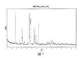
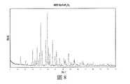
X光繞射法(XRD) 使用D8 Advance A25型繞射儀(Bruker)和CuKα輻射進行根據以下實例所製造之產物的X光繞射測量(XRD)。 基於來自以前為JCPDS(粉末繞射標準之聯合委員會)數據庫的ICDD(國際繞射數據中心)之對應參考繞射圖(Powder Diffraction Files;PDF),確認該產物和其結晶結構。若無法獲得所製造之產物的PDF卡,則使用同型化合物之PDF卡(=相同結構型之化合物)。 元素分析 憑藉使用Axios FAST分光計(PANalytical)之x光螢光分析(XRF)進行元素分析以測定且證實所製造之產物的化學計量。 製造實例1-不含結晶水之Fe2P2O7噴霧粒化具有下列者之懸浮液: i) 35.5kg之氧化鐵(III)-氫氧化物[FeO(OH)或Fe2O31H2O], ii) 16.5kg之98%膦酸[H3PO3], iii) 26.5kg之75%磷酸[H3PO4],及 溶劑220kg之水。以此方式獲得之顆粒在旋轉窯中700℃的形成氣體氛圍(5體積%H2於N2中)下歷平均滯留時間4小時的溫度處理。獲得幾乎無色至稍微粉紅色之產物。該產物之X光繞射圖(XRD)係顯示於圖1中。使用PDF卡01-072-1516確認該產物。 製造實例2-不含結晶水之Mg1.5Fe1.5(PO4)2和Fe3(PO4)2之相混合物 噴霧粒化具有下列者之懸浮液: i) 8.45kg之氧化鐵(III)-氫氧化物[FeO(OH)或Fe2O31H2O], ii) 7.95kg之98%膦酸[H3PO3], iii) 19.6kg之磷酸鐵(III)二水合物[FePO42H2O], iv) 8.43kg之碳酸鎂[MgCO3]及 溶劑160kg之水。以此方式獲得之顆粒在旋轉窯中750℃的形成氣體氛圍(5體積%H2於N2中)下歷平均滯留時間3小時的溫度處理。獲得幾乎無色之產物。該產物之X光繞射圖(XRD)係顯示於圖2中。使用PDF卡確認該產物為主相Mg1.5Fe1.5(PO4)2(PDF卡01-071-6793)和附屬相Fe3(PO4)2(PDF卡00-49-1087)之相混合物。 製造實例3-不含結晶水之Fe3(PO4)2噴霧粒化具有下列者之懸浮液: i) 21.75kg之氧化鐵(III)-氫氧化物[FeO(OH)或Fe2O31H2O], ii) 12.15kg之98%膦酸[H3PO3], iii) 10.3kg之磷酸鐵(III)二水合物[FePO42H2O],及 溶劑:140kg之水。以此方式獲得之顆粒在旋轉窯中750℃的形成氣體氛圍(5體積%H2於N2中)下歷平均滯留時間90分鐘的溫度處理。獲得幾乎無色之產物。該產物之X光繞射圖(XRD)係顯示於圖3中。該產物結晶成磷鐵錳礦結構且使用PDF卡00-49-1087確認該產物。研磨該產物,使得50重量%之該產物具有小於3μm的粒度。該經研磨之產物的粒度分布係顯示於圖9中。 製造實例4-不含結晶水之KFe(PO4)的製造 噴霧粒化具有下列者之懸浮液: i) 11.80kg之氧化鐵(III)-氫氧化物[FeO(OH)或Fe2O31H2O], ii) 10.70kg之98%膦酸[H3PO3], iii) 24.8kg之磷酸鐵(III)二水合物[FePO42H2O], IV) 29.8kg之50%鹼液[KOH], V) 1.0kg之75%磷酸[H3PO4],及 溶劑:110kg之水。以此方式獲得之顆粒在旋轉窯中650℃的形成氣體氛圍(5體積%H2於N2中)下歷平均滯留時間3小時的溫度處理。獲得淡淺綠色產物。該產物之X光繞射圖(XRD)係顯示於圖4中。使用PDF卡01-076-4615確認該產物。 製造實例5-不含結晶水之KFe0.90Zn0.10(PO4) 噴霧粒化具有下列者之懸浮液: i) 10.60kg之氧化鐵(III)-氫氧化物[FeO(OH)或Fe2O31H2O], ii) 9.65kg之98%膦酸[H3PO3], iii) 22.30kg之磷酸鐵(III)二水合物[FePO42H2O], IV) 2.15kg之氧化鋅[ZnO], IV) 29.8kg之50%鹼液[KOH], V) 4.15kg之75%磷酸[H3PO4],及 溶劑:120kg之水。以此方式獲得之顆粒在旋轉窯中600℃的形成氣體氛圍(5體積%H2於N2中)下歷平均滯留時間2小時的溫度處理。獲得淺灰色產物。該產物之X光繞射圖(XRD)係顯示於圖5中。該產物是新的結構型,其明顯與根據PDF卡01-076-4615之KFe(PO4)結構密切相關。 製造實例6-不含結晶水之KFe0.75Zn0.25(PO4) 噴霧粒化具有下列者之懸浮液: i) 8.85kg之氧化鐵(III)-氫氧化物[FeO(OH)或Fe2O31H2O], ii) 8.05kg之98%膦酸[H3PO3], iii) 18.60kg之磷酸鐵(III)二水合物[FePO42H2O], IV) 5.40kg之氧化鋅[ZnO], IV) 29.8kg之50%鉀鹼液[KOH], V) 9.30kg之75%磷酸[H3PO4],及 溶劑:120kg之水。以此方式獲得之顆粒在旋轉窯中600℃的形成氣體氛圍(5體積%H2於N2中)下歷平均滯留時間2小時的溫度處理。獲得淺灰色產物。該產物之X光繞射圖(XRD)係顯示於圖6中。該產物無法從文獻得知。其以同型的方式結晶以形成根據PDF卡01-081-1034之KZn (PO4)。 製造實例7-不含結晶水之KFe0.75Mn0.25(PO4) 噴霧粒化具有下列者之懸浮液: i) 8.85kg之氧化鐵(III)-氫氧化物[FeO(OH)或Fe2O31H2O], ii) 8.05kg之98%膦酸[H3PO3], iii) 18.60kg之磷酸鐵(III)二水合物[FePO42H2O], IV) 8.85kg之碳酸錳水合物[MnCO3H2O], IV) 29.8kg之50%鹼液[KOH], V) 9.30kg之75%磷酸[H3PO4],及 溶劑:140kg之水。以此方式獲得之顆粒在旋轉窯中600℃的形成氣體氛圍(5體積%H2於N2中)下歷平均滯留時間2小時的溫度處理。獲得淺灰色產物。該產物之X光繞射圖(XRD)係顯示於圖7中。該產物無法從文獻得知。其以同型的方式結晶成根據PDF卡01-076-4615之KFe(PO4)。 製造實例8-不含結晶水之BaFeP2O7噴霧粒化具有下列者之懸浮液: i) 8.70kg之氧化鐵(III)-氫氧化物[FeO(OH)或Fe2O31H2O], ii) 8.20kg之98%膦酸[H3PO3], iii) 19.05kg之磷酸鐵(III)二水合物[FePO42H2O], IV) 63.09kg之氫氧化鋇八水合物[Ba(OH)28H2O], V) 26.15kg之75%磷酸[H3PO4],及 溶劑:250kg之水。以此方式獲得之顆粒在旋轉窯中800℃的形成氣體氛圍(5體積%H2於N2中)下歷平均滯留時間4小時的溫度處理。獲得淺灰色產物。該產物之X光繞射圖(XRD)係顯示於圖8中。產物以同型的方式結晶以形成根據PDF卡01-084-1833之BaCoP2O7。 下列實例說明根據本發明之方法 實例1 1 kg之磷酸氫氧化銅與100 g之二氧化鈦放置在具有水之反應器中且被攪拌1小時。所得之製備物被過濾且在約120℃下乾燥直至水含量最高0.5重量%。所得之粉末與1重量%磷酸二氫二鈉(Na2H2P2O7)乾混合。使用擠出機(Coperion GmbH製之ZSK 18型)將5重量%該混合物加工於Sabic 所製之PC/ABS共聚物(LNPTMCOLORCOMPTMCompound NX05467)中。然後該塑膠在射出成形機的輔助下處理以形成約2 mm厚的板。該等板以具有1064 nm波長的Nd:YAG雷射(Trumpf)照射且產生結構。進行均勻金屬分離(金屬核),其適合作為傳導路徑或傳導路徑之先質。 實例2 式Fe2Mg(PO4)2之磷酸鐵(II)鎂與1重量%磷酸二氫二鈉(Na2H2P2O7)乾混合。使用擠出機(Coperion GmbH製之ZSK 18型)將5重量%該混合物加工於聚醯胺6.6(BASF製之UltramidTM)中且製造顆粒。然後進一步處理該顆粒以形成3 cm × 4 cm × 3 mm的板。該等板以具有1064 nm波長的Nd:YAG雷射(Trumpf)照射且產生導電結構。 實例3(比較用) 使用擠出機(Coperion GmbH製之ZSK 18型)將3重量%磷酸氫氧化銅加工於聚醯胺6.6(BASF製之UltramidTM)中。該擠出作用係在所推薦之溫度範圍的上端(285℃)進行。在此情況下,該塑膠有非所欲之褪色。起初稍微帶綠色之化合物之顏色改變成棕色。此外發現在該擠出機軸上有輕微但非所欲之金屬銅分離。 實例4 使用擠出機(Coperion GmbH製之ZSK 18型)將4重量%磷酸氫氧化銅和2重量%硫酸鈉鋁(SAS)加工於聚醯胺6.6 (BASF製之UltramidTM)中且製造顆粒。該擠出作用係在所推薦之溫度範圍的上端(285℃)進行。然後進一步處理該顆粒以形成約3 cm × 4 cm × 3 mm的板。在該塑膠中沒有非所欲之褪色且在該擠出機軸上沒有沉積金屬銅。該等板以具有1064 nm波長的Nd:YAG雷射(Trumpf)照射且產生結構。均勻形成適合作為傳導路徑或傳導路徑之先質之傳導結構。 實例5 使用擠出機(Coperion GmbH製之ZSK 18型)將40重量%正磷酸鐵(II)(Fe3(PO4)2)和1重量%硫酸鈉鋁(SAS)加工於LDPE(LyondellBasell製之LupolenTM1800 S)中且製造顆粒。然後進一步處理該等顆粒以形成3 cm × 4 cm × 3 mm的板。該塑膠稍帶綠色,但在該擠出機軸上沒有沉積。該等板以具有1064 nm波長的Nd:YAG雷射(Trumpf)照射且產生結構。均勻形成適合作為傳導路徑或傳導路徑之先質之傳導結構。X-ray diffraction (XRD) X-ray diffraction measurements (XRD) of the products produced according to the following examples were carried out using a D8 Advance A25 diffractometer (Bruker) and CuKα radiation. The product and its crystalline structure were confirmed based on corresponding reference diffraction patterns (Powder Diffraction Files; PDF) from ICDD (International Centre for Diffraction Data) formerly the JCPDS (Joint Committee on Powder Diffraction Standards) database. If a PDF card of the manufactured product is not available, a PDF card of the compound of the same type (= compound of the same structural type) is used. Elemental Analysis Elemental analysis was performed by means of x-ray fluorescence analysis (XRF) using an Axios FAST spectrometer (PANalytical) to determine and confirm the stoichiometry of the products produced. Production Example 1 - Fe2 P2 O7 without crystal water spray granulation of a suspension with: i) 35.5 kg of iron(III) oxide-hydroxide [FeO (OH) orFe2O3 1H2 O], ii) 16.5 kg of 98% phosphonic acid [H3 PO3 ], iii) 26.5 kg of 75% phosphoric acid [H3 PO4 ], and solvent 220 kg of water. The granules obtained in this way were treated in a rotary kiln at a temperature of 700° C. under a forming gas atmosphere (5% by volume H2 in N2 ) with an average residence time of 4 hours. An almost colorless to slightly pink product was obtained. The X-ray diffraction pattern (XRD) of the product is shown in FIG. 1 . The product was confirmed using PDF card 01-072-1516. Production Example 2 - Phase Mixture of Mg1.5 Fe1.5 (PO4 )2 and Fe3 (PO4 )2 without Crystalline Water Spray Granulation Suspension with: i) 8.45 kg of Iron(III) Oxide- Hydroxide [FeO(OH) or Fe2 O3 1H2 O], ii) 7.95 kg of 98% phosphonic acid [H3 PO3 ], iii) 19.6 kg of iron(III) phosphate dihydrate [FePO4 2H2 O], iv) 8.43 kg of magnesium carbonate [MgCO3 ] and solvent 160 kg of water. The granules obtained in this way were treated in a rotary kiln at a temperature of 750° C. under a forming gas atmosphere (5 vol % H2 in N2 ) with an average residence time of 3 hours. An almost colorless product was obtained. The X-ray diffraction pattern (XRD) of the product is shown in FIG. 2 . The product was confirmed using a PDF card as a phase mixture of the main phase Mg1.5 Fe1.5 (PO4 )2 (PDF card 01-071-6793) and the subsidiary phase Fe3 (PO4 )2 (PDF card 00-49-1087). Production Example3- Fe3 (PO4 )2 Spray Granulation without Crystal Water 1H2 O], ii) 12.15 kg of 98% phosphonic acid [H3 PO3 ], iii) 10.3 kg of iron(III) phosphate dihydrate [FePO4 2H2 O], and solvent: 140 kg of water. The granules obtained in this way were treated in a rotary kiln at a temperature of 750° C. under a forming gas atmosphere (5% by volume H2 in N2 ) with an average residence time of 90 minutes. An almost colorless product was obtained. The X-ray diffraction pattern (XRD) of the product is shown in FIG. 3 . The product crystallized into a ferromenite structure and was identified using PDF card 00-49-1087. The product was ground so that 50% by weight of the product had a particle size of less than 3 μm. The particle size distribution of the milled product is shown in FIG. 9 . Production Example 4 - Production of KFe(PO4 ) without crystal water Spray granulation of a suspension with: i) 11.80 kg of iron(III) oxide-hydroxide [FeO(OH) or Fe2 O3 1H2 O], ii) 10.70 kg of 98% phosphonic acid [H3 PO3 ], iii) 24.8 kg of iron(III) phosphate dihydrate [FePO4 2H2 O], IV) 29.8 kg of 50% base liquid [KOH], V) 1.0 kg of 75% phosphoric acid [H3 PO4 ], and solvent: 110 kg of water. The granules obtained in this way were treated in a rotary kiln at a temperature of 650° C. under a forming gas atmosphere (5% by volume H2 in N2 ) with an average residence time of 3 hours. A pale green product was obtained. The X-ray diffraction pattern (XRD) of the product is shown in FIG. 4 . The product was confirmed using PDF card 01-076-4615. Production Example 5 - KFe0.90 Zn0.10 (PO4 ) without crystal water spray granulation of a suspension with: i) 10.60 kg of iron(III)oxide -hydroxide [FeO(OH) or Fe2O3 1H2 O], ii) 9.65 kg of 98% phosphonic acid [H3 PO3 ], iii) 22.30 kg of iron(III) phosphate dihydrate [FePO4 2H2 O], IV) 2.15 kg of zinc oxide [ZnO], IV) 29.8 kg of 50% lye [KOH], V) 4.15 kg of 75% phosphoric acid [H3 PO4 ], and solvent: 120 kg of water. The granules obtained in this way were treated in a rotary kiln at a temperature of 600° C. under a forming gas atmosphere (5% by volume H2 in N2 ) with an average residence time of 2 hours. A light grey product is obtained. The X-ray diffraction pattern (XRD) of the product is shown in FIG. 5 . This product is a new structural type which is apparently closely related to the KFe(PO4 ) structure according to PDF card 01-076-4615. Production Example 6 - KFe0.75 Zn0.25 (PO4 ) without crystal water spray granulation of a suspension with: i) 8.85 kg of iron(III)oxide -hydroxide [FeO(OH) or Fe2O3 1H2 O], ii) 8.05 kg of 98% phosphonic acid [H3 PO3 ], iii) 18.60 kg of iron(III) phosphate dihydrate [FePO4 2H2 O], IV) 5.40 kg of zinc oxide [ZnO], IV) 29.8 kg of 50% potassium lye [KOH], V) 9.30 kg of 75% phosphoric acid [H3 PO4 ], and solvent: 120 kg of water. The granules obtained in this way were treated in a rotary kiln at a temperature of 600° C. under a forming gas atmosphere (5% by volume H2 in N2 ) with an average residence time of 2 hours. A light grey product is obtained. The X-ray diffraction pattern (XRD) of the product is shown in FIG. 6 . This product is not known from the literature. It crystallized in an isomorphic manner to form KZn(PO4 ) according to PDF card 01-081-1034. Production Example 7 - KFe0.75 Mn0.25 (PO4 ) without crystal water spray granulation of a suspension having: i) 8.85 kg of iron(III)oxide -hydroxide [FeO(OH) or Fe2O3 1H2 O], ii) 8.05 kg of 98% phosphonic acid [H3 PO3 ], iii) 18.60 kg of iron(III) phosphate dihydrate [FePO4 2H2 O], IV) 8.85 kg of manganese carbonate Hydrate [MnCO3 H2 O], IV) 29.8 kg of 50% lye [KOH], V) 9.30 kg of 75% phosphoric acid [H3 PO4 ], and solvent: 140 kg of water. The granules obtained in this way were treated in a rotary kiln at a temperature of 600° C. under a forming gas atmosphere (5% by volume H2 in N2 ) with an average residence time of 2 hours. A light grey product is obtained. The X-ray diffraction pattern (XRD) of the product is shown in FIG. 7 . This product is not known from the literature. It crystallized isomorphically as KFe(PO4 ) according to PDF card 01-076-4615. Production Example 8 - BaFeP2 O7 without crystal water spray granulation of a suspension with: i) 8.70 kg of iron(III) oxide-hydroxide [FeO(OH) or Fe2 O3 1H2 O ], ii) 8.20 kg of 98% phosphonic acid [H3 PO3 ], iii) 19.05 kg of iron(III) phosphate dihydrate [FePO4 2H2 O], IV) 63.09 kg of barium hydroxide octahydrate [Ba(OH)2 8H2 O], V) 26.15 kg of 75% phosphoric acid [H3 PO4 ], and solvent: 250 kg of water. The granules obtained in this way were treated in a rotary kiln at a temperature of 800° C. under a forming gas atmosphere (5% by volume H2 in N2 ) with an average residence time of 4 hours. A light grey product is obtained. The X-ray diffraction pattern (XRD) of the product is shown in FIG. 8 . The product crystallized isomorphically to form BaCoP2 O7 according to PDF card 01-084-1833. The following examples illustrate the method according to the invention Example 1 1 kg of copper hydroxide phosphate and 100 g of titanium dioxide are placed in a reactor with water and stirred for 1 hour. The resulting preparation is filtered and dried at about 120° C. up to a water content of up to 0.5% by weight. The resulting powder was dry blended with 1% by weight of disodium dihydrogen phosphate (Na2 H2 P2 O7 ). 5% by weight of this mixture was processed into a PC/ABS copolymer (LNP™ COLORCOMP™ Compound NX05467) by Sabic using an extruder (ZSK 18 model from Coperion GmbH). The plastic was then processed with the aid of an injection molding machine to form sheets of approximately 2 mm thickness. The plates were irradiated with a Nd:YAG laser (Trumpf) with a wavelength of 1064 nm and the structures were created. A uniform metal separation (metal core) is carried out, which is suitable as a conductive path or precursor of a conductive path. Example 2 Magnesium iron(II) phosphate of formula Fe2 Mg(PO4 )2 was dry mixed with 1 wt% disodium dihydrogen phosphate (Na2 H2 P2 O7 ). 5% by weight of this mixture was processed into polyamide 6.6 (Ultramid™ from BASF) using an extruder (model ZSK 18 from Coperion GmbH) and pellets were produced. The particles were then further processed to form 3 cm x 4 cm x 3 mm plates. The plates were irradiated with a Nd:YAG laser (Trumpf) with a wavelength of 1064 nm and conductive structures were created. Example 3 (comparative) 3% by weight of copper hydroxide phosphate was processed into polyamide 6.6 (Ultramid™ from BASF) using an extruder (model ZSK 18 from Coperion GmbH). The extrusion was performed at the upper end of the recommended temperature range (285°C). In this case, the plastic had unintended discoloration. The color of the initially slightly greenish compound changed to brown. A slight but undesired separation of metallic copper was also found on the extruder shaft. Example 4 Processing of 4 wt% copper hydroxide phosphate and 2 wt% sodium aluminium sulfate (SAS) in polyamide 6.6 (Ultramid™ from BASF) using an extruder (Model ZSK 18 from Coperion GmbH) and production of granules . The extrusion was performed at the upper end of the recommended temperature range (285°C). The particles were then further processed to form plates of approximately 3 cm x 4 cm x 3 mm. There was no unwanted discoloration in the plastic and no metallic copper deposits on the extruder shaft. The plates were irradiated with a Nd:YAG laser (Trumpf) with a wavelength of 1064 nm and the structures were created. A conductive structure suitable as a conductive path or precursor of a conductive path is uniformly formed. Example 5 40% by weight of iron(II) orthophosphate (Fe3 (PO4 )2 ) and 1% by weight of sodium aluminum sulfate (SAS) were processed into LDPE (manufactured by LyondellBasell) using an extruder (model ZSK 18 by Coperion GmbH). in Lupolen™ 1800 S) and granules were produced. The particles were then further processed to form 3 cm x 4 cm x 3 mm plates. The plastic was slightly greenish, but did not deposit on the extruder shaft. The plates were irradiated with a Nd:YAG laser (Trumpf) with a wavelength of 1064 nm and the structures were created. A conductive structure suitable as a conductive path or precursor of a conductive path is uniformly formed.
圖1顯示根據本發明符合製造實例1所製造之不含結晶水之Fe2P2O7的X光繞射圖。 圖2顯示根據本發明符合製造實例2所製造之不含結晶水之Mg1.5Fe1.5(PO4)2和Fe3(PO4)2之相混合物的X光繞射圖。 圖3顯示根據本發明符合製造實例3所製造之不含結晶水之Fe3(PO4)2的X光繞射圖。 圖4顯示根據本發明符合製造實例4所製造之不含結晶水之KFe(PO4)的X光繞射圖。 圖5顯示根據本發明符合製造實例5所製造之不含結晶水之KFe0.90Zn0.10(PO4)的X光繞射圖。 圖6顯示根據本發明符合製造實例6所製造之不含結晶水之KFe0.75Zn0.25(PO4)的X光繞射圖。 圖7顯示根據本發明符合製造實例7所製造之不含結晶水之KFe0.75Mn0.25(PO4)的X光繞射圖。 圖8顯示根據本發明符合製造實例8所製造之不含結晶水之BaFeP2O7的X光繞射圖。FIG. 1 shows the X-ray diffraction pattern of Fe2 P2 O7 without crystal water produced in accordance with Production Example 1 according to the present invention. 2 shows the X-ray diffraction pattern of the phase mixture of Mg1.5 Fe1.5 (PO4 )2 and Fe3 (PO4 )2 without crystal water produced according to the present invention in accordance with Production Example 2. 3 shows the X-ray diffraction pattern of Fe3 (PO4 )2 without crystal water produced in accordance with Production Example 3 according to the present invention. FIG. 4 shows the X-ray diffraction pattern of KFe(PO4 ) without crystal water produced in accordance with Production Example 4 according to the present invention. 5 shows the X-ray diffraction pattern of KFe0.90 Zn0.10 (PO4 ) without crystal water produced in accordance with Production Example 5 according to the present invention. 6 shows the X-ray diffraction pattern of KFe0.75 Zn0.25 (PO4 ) without crystal water produced in accordance with Production Example 6 according to the present invention. 7 shows the X-ray diffraction pattern of KFe0.75 Mn0.25 (PO4 ) without crystal water produced in accordance with Production Example 7 according to the present invention. FIG. 8 shows the X-ray diffraction pattern of BaFeP2 O7 without crystal water produced in accordance with Production Example 8 according to the present invention.
Claims (14)
Translated fromChinese
Applications Claiming Priority (3)
| Application Number | Priority Date | Filing Date | Title |
|---|---|---|---|
| DE102017106913.5ADE102017106913A1 (en) | 2017-03-30 | 2017-03-30 | Process for the production of electrically conductive structures on a carrier material |
| ??102017106913.5 | 2017-03-30 | ||
| DE102017106913.5 | 2017-03-30 |
Publications (2)
| Publication Number | Publication Date |
|---|---|
| TW201843029A TW201843029A (en) | 2018-12-16 |
| TWI757450Btrue TWI757450B (en) | 2022-03-11 |
Family
ID=61827734
Family Applications (1)
| Application Number | Title | Priority Date | Filing Date |
|---|---|---|---|
| TW107109229ATWI757450B (en) | 2017-03-30 | 2018-03-19 | Method for manufacturing electrically conductive structures on a carrier material |
Country Status (10)
| Country | Link |
|---|---|
| US (1) | US11718727B2 (en) |
| EP (1) | EP3601642A1 (en) |
| JP (2) | JP7213823B2 (en) |
| KR (1) | KR102665005B1 (en) |
| CN (1) | CN110475911A (en) |
| DE (1) | DE102017106913A1 (en) |
| EA (1) | EA201991999A1 (en) |
| MX (1) | MX2019011516A (en) |
| TW (1) | TWI757450B (en) |
| WO (1) | WO2018178022A1 (en) |
Families Citing this family (12)
| Publication number | Priority date | Publication date | Assignee | Title |
|---|---|---|---|---|
| DE102017106912A1 (en)* | 2017-03-30 | 2018-10-04 | Chemische Fabrik Budenheim Kg | Process for the preparation of Fe (II) P / Fe (II) MetP compounds |
| DE102017106913A1 (en) | 2017-03-30 | 2018-10-04 | Chemische Fabrik Budenheim Kg | Process for the production of electrically conductive structures on a carrier material |
| DE102017106911A1 (en) | 2017-03-30 | 2018-10-04 | Chemische Fabrik Budenheim Kg | Use of water-free Fe (II) compounds as radiation absorbers |
| DE102018124344A1 (en)* | 2018-10-02 | 2020-04-02 | Chemische Fabrik Budenheim Kg | Conductive textiles |
| CN110137183A (en) | 2019-04-23 | 2019-08-16 | 深圳市华星光电技术有限公司 | Array substrate and manufacturing method thereof |
| CN110029382B (en)* | 2019-05-22 | 2021-09-24 | 电子科技大学 | A surface treatment process for direct electroplating and related direct electroplating process |
| TWI706593B (en)* | 2019-10-02 | 2020-10-01 | 川升股份有限公司 | Antenna device |
| CN112636011A (en)* | 2019-10-08 | 2021-04-09 | 川升股份有限公司 | Radio frequency assembly combination and antenna device |
| DE102020111158A1 (en)* | 2020-04-23 | 2021-10-28 | Chemische Fabrik Budenheim Kg | Use of an additive in the production of copper (II) hydroxide phosphate |
| CN111805091A (en)* | 2020-06-09 | 2020-10-23 | 深圳市信维通信股份有限公司 | LAP laser etching process |
| CN113105054A (en)* | 2021-04-09 | 2021-07-13 | 瀚蓝工业服务(嘉兴)有限公司 | Method for comprehensively recycling phosphorus-containing waste acid and iron-containing etching waste liquid |
| CN114479410B (en)* | 2022-02-16 | 2023-08-04 | 无锡赢同新材料科技有限公司 | Low dielectric loss LDS engineering plastic and preparation method thereof |
Citations (2)
| Publication number | Priority date | Publication date | Assignee | Title |
|---|---|---|---|---|
| CN105492214A (en)* | 2013-06-21 | 2016-04-13 | 沙特基础全球技术有限公司 | Flame retardant laser direct structuring materials |
| CN105899609A (en)* | 2014-12-01 | 2016-08-24 | Lg化学株式会社 | Polycarbonate resin composition and preparation method therefor |
Family Cites Families (42)
| Publication number | Priority date | Publication date | Assignee | Title |
|---|---|---|---|---|
| DE3917294A1 (en) | 1989-05-27 | 1990-11-29 | Huels Chemische Werke Ag | HIGH POLYMERS MATERIALS LABELABLE WITH LASER LIGHT |
| US5063011A (en) | 1989-06-12 | 1991-11-05 | Hoeganaes Corporation | Doubly-coated iron particles |
| US5489639A (en) | 1994-08-18 | 1996-02-06 | General Electric Company | Copper salts for laser marking of thermoplastic compositions |
| US5939039A (en) | 1997-01-16 | 1999-08-17 | Orthovita, Inc. | Methods for production of calcium phosphate |
| DE19723734C2 (en) | 1997-06-06 | 2002-02-07 | Gerhard Naundorf | Conductor structures on a non-conductive carrier material and method for their production |
| US6383519B1 (en) | 1999-01-26 | 2002-05-07 | Vita Special Purpose Corporation | Inorganic shaped bodies and methods for their production and use |
| DE50008242D1 (en) | 2000-09-26 | 2004-11-18 | Enthone Omi Deutschland Gmbh | Process for the selective metallization of dielectric materials |
| DE10053639B4 (en) | 2000-10-28 | 2007-04-12 | Chemische Fabrik Budenheim Kg | Use of iron, cobalt, nickel or molybdenum salts |
| DE10132092A1 (en) | 2001-07-05 | 2003-01-23 | Lpkf Laser & Electronics Ag | Track structures and processes for their manufacture |
| DE10356334B4 (en)* | 2003-11-28 | 2016-02-11 | Sachtleben Chemie Gmbh | Use of thermoplastic, polymeric materials with high IR absorption |
| SI1790701T2 (en) | 2005-11-25 | 2012-05-31 | Sicpa Holding Sa | IR-absorbing intaglio ink |
| DE102006038043A1 (en)* | 2006-08-14 | 2008-02-21 | Chemische Fabrik Budenheim Kg | Laser inscribable polymer material |
| DE102007012725A1 (en) | 2007-03-16 | 2008-09-18 | Basf Se | Polynary metal oxide phosphate |
| DE102007012724A1 (en) | 2007-03-16 | 2008-09-18 | Basf Se | Polynary metal oxide phosphate |
| DE102007012723A1 (en) | 2007-03-16 | 2008-09-18 | Basf Se | Polynary vanadyl pyrophosphate |
| US8168329B2 (en) | 2007-06-18 | 2012-05-01 | Advanced Lithium Electrochemistry Co., Ltd. | Electrochemical composition and associated technology |
| US8309640B2 (en)* | 2008-05-23 | 2012-11-13 | Sabic Innovative Plastics Ip B.V. | High dielectric constant laser direct structuring materials |
| TWI474970B (en) | 2008-12-29 | 2015-03-01 | Basf Se | Synthesis of lithium-metal-phosphates under hydrothermal conditions |
| DE102009001335A1 (en) | 2009-03-04 | 2010-09-09 | Chemische Fabrik Budenheim Kg | Radiation absorbing material |
| EP2408865B2 (en)* | 2009-03-18 | 2017-10-11 | Merck Patent GmbH | Pigment for laser marking |
| CN101659406B (en) | 2009-09-25 | 2011-05-11 | 四川大学 | Method for preparing iron phosphate from ferrophosphorus |
| EP2516550B1 (en)* | 2009-12-21 | 2014-07-02 | Mitsubishi Chemical Europe GmbH | Aromatic Polycarbonate Composition |
| US9139429B2 (en) | 2010-03-02 | 2015-09-22 | Guiqing Huang | High performance cathode material LiFePO4, its precursors and methods of making thereof |
| DE102010003366A1 (en)* | 2010-03-26 | 2011-09-29 | Chemische Fabrik Budenheim Kg | Laser-induced plastic foams |
| EP2632689B2 (en)* | 2010-10-26 | 2022-03-23 | Basell Poliolefine Italia S.r.l. | Process for producing injection stretch blow molded polyolefin containers |
| CN103154135B (en)* | 2011-03-18 | 2014-10-15 | 三菱化学欧洲合资公司 | Process for producing circuit carrier |
| DE102011056815A1 (en) | 2011-12-21 | 2013-08-01 | Chemische Fabrik Budenheim Kg | Nutrient composition for biological systems |
| DE102013100583A1 (en) | 2013-01-21 | 2014-07-24 | Chemische Fabrik Budenheim Kg | Susceptor systems for packaging materials |
| US9944768B2 (en) | 2013-04-01 | 2018-04-17 | Sabic Global Technologies B.V. | High modulus laser direct structuring polycarbonate composites with enhanced plating performance and broad laser window and methods for the manufacture and use thereof |
| DE102013112387B3 (en) | 2013-11-11 | 2014-12-24 | Chemische Fabrik Budenheim Kg | Doped copper II hydroxide phosphate, process for its preparation and use |
| WO2015079385A1 (en)* | 2013-11-27 | 2015-06-04 | Sabic Global Technologies B.V. | High modulus laser direct structuring polycarbonate composites with enhanced plating performance and broad laser window by reflection additives |
| EP2886605B2 (en) | 2013-12-20 | 2021-09-01 | Ems-Chemie Ag | Plastic moulding material and use of same |
| US9676927B2 (en)* | 2014-04-09 | 2017-06-13 | The Shepherd Color Company | Core-shell composite inorganic metal oxides and method of preparing for prevention of thermal oxidative degradation in polymer and resin compositions |
| WO2016034000A1 (en)* | 2014-09-04 | 2016-03-10 | Byd Company Limited | Polymer composition, ink composition and method for selectively metallizing insulating substrate |
| KR101722744B1 (en) | 2014-10-23 | 2017-04-03 | 주식회사 엘지화학 | Composition for forming conductive pattern by irradiation of electromagnetic wave |
| CN104387738B (en)* | 2014-11-19 | 2016-08-17 | 东莞市三条化成实业有限公司 | A kind of preparation method of the laser powder of white laser straight forming material |
| WO2016092472A1 (en)* | 2014-12-12 | 2016-06-16 | Sabic Global Technologies B.V. | Laser-direct structuring of polymeric films and sheets and methods of making |
| WO2016189023A1 (en)* | 2015-05-28 | 2016-12-01 | Dsm Ip Assets B.V. | A thermoplastic polymer composition, an article made thereof and a process for preparing the same |
| JP6749174B2 (en) | 2015-09-03 | 2020-09-02 | 三菱エンジニアリングプラスチックス株式会社 | Polyester resin composition for laser direct structuring |
| DE102017106912A1 (en) | 2017-03-30 | 2018-10-04 | Chemische Fabrik Budenheim Kg | Process for the preparation of Fe (II) P / Fe (II) MetP compounds |
| DE102017106911A1 (en)* | 2017-03-30 | 2018-10-04 | Chemische Fabrik Budenheim Kg | Use of water-free Fe (II) compounds as radiation absorbers |
| DE102017106913A1 (en) | 2017-03-30 | 2018-10-04 | Chemische Fabrik Budenheim Kg | Process for the production of electrically conductive structures on a carrier material |
- 2017
- 2017-03-30DEDE102017106913.5Apatent/DE102017106913A1/ennot_activeWithdrawn
- 2018
- 2018-03-19TWTW107109229Apatent/TWI757450B/enactive
- 2018-03-26EAEA201991999Apatent/EA201991999A1/enunknown
- 2018-03-26USUS16/496,591patent/US11718727B2/enactiveActive
- 2018-03-26EPEP18714226.0Apatent/EP3601642A1/enactivePending
- 2018-03-26WOPCT/EP2018/057662patent/WO2018178022A1/ennot_activeCeased
- 2018-03-26MXMX2019011516Apatent/MX2019011516A/enunknown
- 2018-03-26JPJP2019553862Apatent/JP7213823B2/enactiveActive
- 2018-03-26KRKR1020197028590Apatent/KR102665005B1/enactiveActive
- 2018-03-26CNCN201880023260.7Apatent/CN110475911A/enactivePending
- 2022
- 2022-10-28JPJP2022173332Apatent/JP7376667B2/enactiveActive
Patent Citations (2)
| Publication number | Priority date | Publication date | Assignee | Title |
|---|---|---|---|---|
| CN105492214A (en)* | 2013-06-21 | 2016-04-13 | 沙特基础全球技术有限公司 | Flame retardant laser direct structuring materials |
| CN105899609A (en)* | 2014-12-01 | 2016-08-24 | Lg化学株式会社 | Polycarbonate resin composition and preparation method therefor |
Also Published As
| Publication number | Publication date |
|---|---|
| EA201991999A1 (en) | 2020-02-28 |
| US20200032028A1 (en) | 2020-01-30 |
| MX2019011516A (en) | 2020-02-05 |
| JP7376667B2 (en) | 2023-11-08 |
| EP3601642A1 (en) | 2020-02-05 |
| US11718727B2 (en) | 2023-08-08 |
| JP2020515717A (en) | 2020-05-28 |
| TW201843029A (en) | 2018-12-16 |
| JP7213823B2 (en) | 2023-01-27 |
| WO2018178022A1 (en) | 2018-10-04 |
| KR20190133683A (en) | 2019-12-03 |
| KR102665005B1 (en) | 2024-05-10 |
| CN110475911A (en) | 2019-11-19 |
| JP2022187017A (en) | 2022-12-15 |
| DE102017106913A1 (en) | 2018-10-04 |
Similar Documents
| Publication | Publication Date | Title |
|---|---|---|
| TWI757450B (en) | Method for manufacturing electrically conductive structures on a carrier material | |
| TWI544499B (en) | Composition and method for forming conductive pattern, and resin structure having conductive pattern thereon | |
| TWI527943B (en) | Composition and method for forming conductive pattern, and resin structure having conductive pattern thereon | |
| WO2014175599A1 (en) | Composition for forming conductive pattern, method for forming conductive pattern using same, and resin structure having conductive pattern | |
| KR20150060555A (en) | Composition for forming conductive pattern and resin structure having conductive pattern thereon | |
| EP3601423A1 (en) | Use of fe(ii) compounds which are free from water of crystallisation as radiation absorber | |
| US10065860B2 (en) | Composition for forming conductive pattern and resin structure having conductive pattern | |
| HK40015102A (en) | Method for producing electrically conductive structures on a carrier material | |
| JP6224842B2 (en) | Conductive pattern forming composition and resin structure having conductive pattern | |
| KR102114858B1 (en) | A method for manufacturing conductive copper thin-film pattern using laser | |
| KR101983271B1 (en) | Composition for forming conductive pattern and resin structure having conductive pattern thereon | |
| WO2016031404A1 (en) | Composition for electrically conductive film formation use, and method for producing electrically conductive film using same | |
| JP6491318B2 (en) | Conductive pattern forming composition and resin structure having conductive pattern | |
| KR20160026249A (en) | Composition and method for forming conductive pattern, and resin structure having conductive pattern thereon | |
| WO2016043540A1 (en) | Composition for forming conductive patterns and resin structure having conductive pattern |